
MODELLING AND APPLICATION OF SPIRAL
INDUCTORS IN CMOS LC-VCOs
by
Reza Molavi
M.A.Sc., University of British Columbia, 2005
B.Sc., Sharif University of Technology, 2003
A THESIS SUBMITTED IN PARTIAL FULFILMENT OF THE REQUIREMENTS FOR THE DEGREE OF
Doctor of Philosophy
in
The Faculty of Graduate and Postdoctoral Studies
(Electrical and Computer Engineering)
The University of British Columbia (Vancouver)
October 2013
© Reza Molavi, 2013
ii
Abstract
Communication systems are essential components of our everyday lives and they
facilitate accessing and using the ever-increasing amounts of data that have surrounded
us. The main objective of this research is to present solutions at the device, circuit, and
system levels for key passive and active circuit building blocks of communication
systems, namely, monolithic passive inductors and inductor-based voltage-controlled
oscillators (LC-VCOs). These components are almost ubiquitously used in integrated
wireless and wireline communication transceivers, as well as other computing devices.
Key contributions of this work are as follows: In the context of monolithic inductors, we
have studied different inductor structures such as doubly-stacked inductors, vertical
inductors, and coupled-rings. We have developed circuit models to accurately estimate
their inductance and quality factor. The proposed analytical expressions provide
designers with a reasonable estimate of their circuit performance and layout constraints.
The result of proposed analyses is verified by the measurement results of test structures
implemented in CMOS technology.
Regarding LC-VCOs, we have studied the effect of large signal oscillations on such
VCOs by developing a mathematical model to solve the non-linear differential equation
governing the LC tank circuit. The study shows that the VCO frequency and the
amplitude of higher order harmonics are functions of circuit parameters such as the C-V
characteristics of the varactor and the oscillation amplitude. Also, a low- power technique
to boost the output amplitude of push-push VCOs is introduced. Measurement results of a
proof-of-concept prototype test chip in 90-nm CMOS confirm the usefulness of the
proposed technique.
Finally, at the system level, we present an analytical model to study the effect of coupling
between adjacent LC-VCOs closely integrated on the same chip. This is usually the case
in high-speed wireline transceivers such as those used in serial links. The proposed model
explains the behavior of spurious sidebands as observed in the frequency spectrum of
closely-running adjacent links. A redundant frequency mapping scheme is proposed that
iii
significantly reduces this coupling effect. Measurement results of a highly packable clock
synthesizer in a 65-nm CMOS confirm the validity of the analytical model and the
effectiveness of the proposed mapping technique.
iv
Preface
I, Reza Molavi, am the principle contributor of all chapters. Professor Shahriar Mirabbasi
who supervised the research has provided technical consultation and editing assistance on
the manuscript. Dr. Hormoz Djahanshahi also provided technical assistance in the design
of low-power LC-VCOs and reviewed parts of the manuscripts. As described below,
some of the chapters in this thesis have been written based on the following material.
Conference papers:
1. R. Molavi, S. Mirabbasi, and H. Djahanshahi, “A 27-GHz low-power push-push LC
VCO with wide tuning range in 65-nm CMOS,” Proceedings - IEEE International
Symposium on Circuits and Systems, pp. 1141–1144, 2011 (Chapter 3)
2. R. Molavi, S. Mirabbasi, and H. Djahanshahi, “Design and verification of integrated
inductor in CMOS,” 2012 25th IEEE Canadian Conference on Electrical and Computer
Engineering: Vision for a Greener Future, CCECE 2012, 2012 (Chapter 2)
(Best paper finalist)
Journal papers:
1. R. Molavi, S. Mirabbasi, and H. Djahanshahi, “A low power technique to boost the
output amplitude of multi gigahertz push-push LC VCOs,” Microwave and Optical
Technology Letters, vol. 55, no. 7, pp. 1581–1584, July 2013 (Chapter 3)
2. R. Molavi, H. Djahanshahi, R. Zavari, S. Mirabbasi, “Low-Jitter 0.1-to-5.8 GHz Clock
Synthesizer for Area-Efficient Per-Port Integration,” Hindawi Journal of Electrical and
Computer Engineering, vol. 2013 (Aug), Article ID 364982 (Chapter 4)
3. R. Molavi, S. Mirabbas, H. Djahanshahi, “Analysis, Design and verification of fixed
and variable Inductors in bulk CMOS,” to be submitted (Chapter 2)
v
Table of Contents
Abstract .............................................................................................................................. ii
Preface ............................................................................................................................... iv
Table of Contents .............................................................................................................. v
List of Tables ................................................................................................................... vii
List of Figures ................................................................................................................. viii
List of Abbreviations and Terms ................................................................................... xii
Acknowledgements ........................................................................................................ xiv
Dedication ....................................................................................................................... xvi
Chapter 1 Introduction..................................................................................................... 1
1.1 VCOs in Phase-Locked Loops ............................................................................. 3
1.2 Why CMOS? ....................................................................................................... 4
1.3 Contributions ....................................................................................................... 6
1.3.1 Analytical and Device-Level Models for Several Inductor Structures ............... 6
1.3.2 Second Harmonic Analysis and Amplification in Push-Push LC VCOs ............. 7
1.3.3 Coupling Analysis for Densely Integrated PLLs ................................................ 7
1.4 Organization of Thesis ........................................................................................ 8
Chapter 2 Analysis, Design, Simulation and Verification of Integrated Inductors in
Bulk CMOS ....................................................................................................................... 9
2.1 Inductor Modeling .............................................................................................. 10
2.2 Measurement Results of Fixed Inductors ........................................................... 15
2.3 Vertical Inductor for Series Peaking .................................................................. 17
2.4 Variable Inductors .............................................................................................. 20
2.5 Simulation Results.............................................................................................. 27
2.6 Measurement Results ......................................................................................... 31
2.7 Conclusion .......................................................................................................... 33
Chapter 3 Analysis, Design, Optimization and Fabrication of Push-Push LC-VCO
in CMOS .......................................................................................................................... 34
3.1 VCO Architectures ............................................................................................. 35
3.1.1 Ring Oscillators .................................................................................................. 35
3.1.2 LC Oscillators .................................................................................................... 36
3.2 LC-VCO Phase Noise ........................................................................................ 40
3.3 High-Frequency and mm-Wave LC-VCO Design ............................................. 42
3.4 Second Harmonic Generation in AMOS-Based LC tank .................................. 45
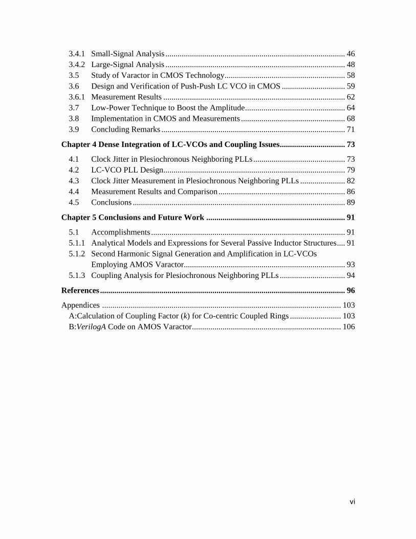
vi
3.4.1 Small-Signal Analysis ........................................................................................ 46
3.4.2 Large-Signal Analysis ........................................................................................ 48
3.5 Study of Varactor in CMOS Technology ........................................................... 58
3.6 Design and Verification of Push-Push LC VCO in CMOS ............................... 59
3.6.1 Measurement Results ......................................................................................... 62
3.7 Low-Power Technique to Boost the Amplitude ................................................. 64
3.8 Implementation in CMOS and Measurements ................................................... 68
3.9 Concluding Remarks .......................................................................................... 71
Chapter 4 Dense Integration of LC-VCOs and Coupling Issues ................................ 73
4.1 Clock Jitter in Plesiochronous Neighboring PLLs ............................................. 73
4.2 LC-VCO PLL Design......................................................................................... 79
4.3 Clock Jitter Measurement in Plesiochronous Neighboring PLLs ...................... 82
4.4 Measurement Results and Comparison .............................................................. 86
4.5 Conclusions ........................................................................................................ 89
Chapter 5 Conclusions and Future Work .................................................................... 91
5.1 Accomplishments ............................................................................................... 91
5.1.1 Analytical Models and Expressions for Several Passive Inductor Structures .... 91
5.1.2 Second Harmonic Signal Generation and Amplification in LC-VCOs
Employing AMOS Varactor............................................................................... 93
5.1.3 Coupling Analysis for Plesiochronous Neighboring PLLs ................................ 94
References ........................................................................................................................ 96
Appendices ..................................................................................................................... 103
A:Calculation of Coupling Factor (k) for Co-centric Coupled Rings ......................... 103
B:VerilogA Code on AMOS Varactor ......................................................................... 106
vii
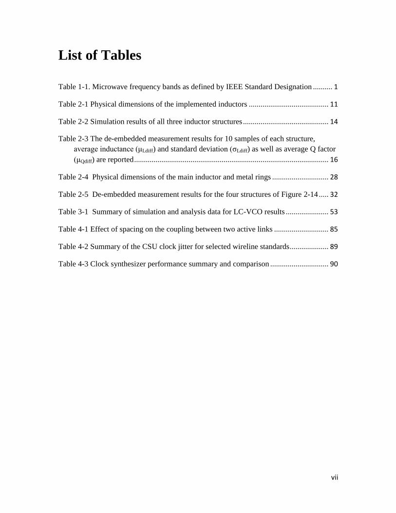
List of Tables
Table 1-1. Microwave frequency bands as defined by IEEE Standard Designation .......... 1
Table 2-1 Physical dimensions of the implemented inductors ......................................... 11
Table 2-2 Simulation results of all three inductor structures ............................................ 14
Table 2-3 The de-embedded measurement results for 10 samples of each structure,
average inductance (μLdiff) and standard deviation (σLdiff) as well as average Q factor
(μQdiff) are reported .................................................................................................... 16
Table 2-4 Physical dimensions of the main inductor and metal rings ............................. 28
Table 2-5 De-embedded measurement results for the four structures of Figure 2-14 ..... 32
Table 3-1 Summary of simulation and analysis data for LC-VCO results ...................... 53
Table 4-1 Effect of spacing on the coupling between two active links ............................ 85
Table 4-2 Summary of the CSU clock jitter for selected wireline standards .................... 89
Table 4-3 Clock synthesizer performance summary and comparison .............................. 90
viii
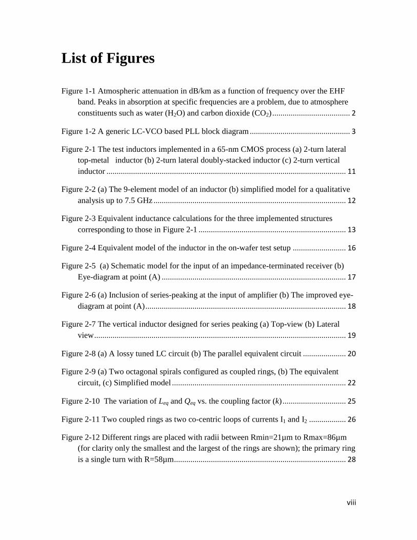
List of Figures
Figure 1-1 Atmospheric attenuation in dB/km as a function of frequency over the EHF
band. Peaks in absorption at specific frequencies are a problem, due to atmosphere
constituents such as water (H2O) and carbon dioxide (CO2) ...................................... 2
Figure 1-2 A generic LC-VCO based PLL block diagram ................................................. 3
Figure 2-1 The test inductors implemented in a 65-nm CMOS process (a) 2-turn lateral
top-metal inductor (b) 2-turn lateral doubly-stacked inductor (c) 2-turn vertical
inductor ..................................................................................................................... 11
Figure 2-2 (a) The 9-element model of an inductor (b) simplified model for a qualitative
analysis up to 7.5 GHz .............................................................................................. 12
Figure 2-3 Equivalent inductance calculations for the three implemented structures
corresponding to those in Figure 2-1 ........................................................................ 13
Figure 2-4 Equivalent model of the inductor in the on-wafer test setup .......................... 16
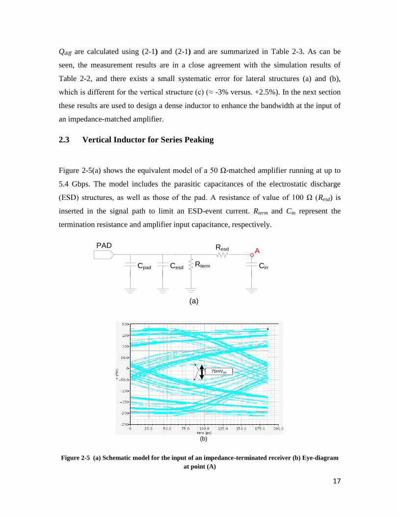
Figure 2-5 (a) Schematic model for the input of an impedance-terminated receiver (b)
Eye-diagram at point (A) .......................................................................................... 17
Figure 2-6 (a) Inclusion of series-peaking at the input of amplifier (b) The improved eye-
diagram at point (A) .................................................................................................. 18
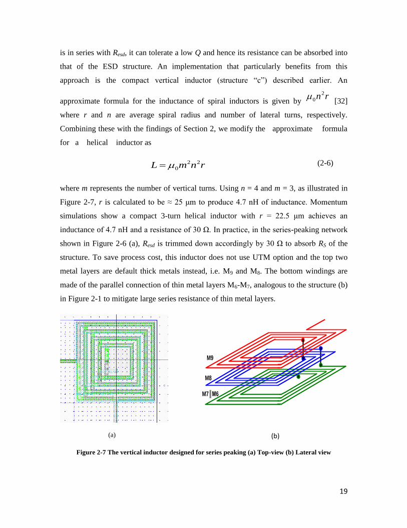
Figure 2-7 The vertical inductor designed for series peaking (a) Top-view (b) Lateral
view ........................................................................................................................... 19
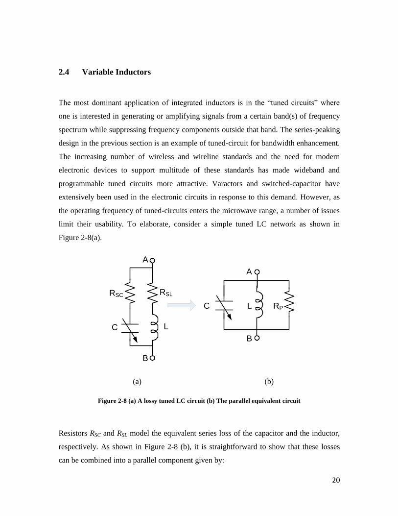
Figure 2-8 (a) A lossy tuned LC circuit (b) The parallel equivalent circuit ..................... 20
Figure 2-9 (a) Two octagonal spirals configured as coupled rings, (b) The equivalent
circuit, (c) Simplified model ..................................................................................... 22
Figure 2-10 The variation of Leq and Qeq vs. the coupling factor (k) ............................... 25
Figure 2-11 Two coupled rings as two co-centric loops of currents I1 and I2 .................. 26
Figure 2-12 Different rings are placed with radii between Rmin=21µm to Rmax=86µm
(for clarity only the smallest and the largest of the rings are shown); the primary ring
is a single turn with R=58µm .................................................................................... 28
ix
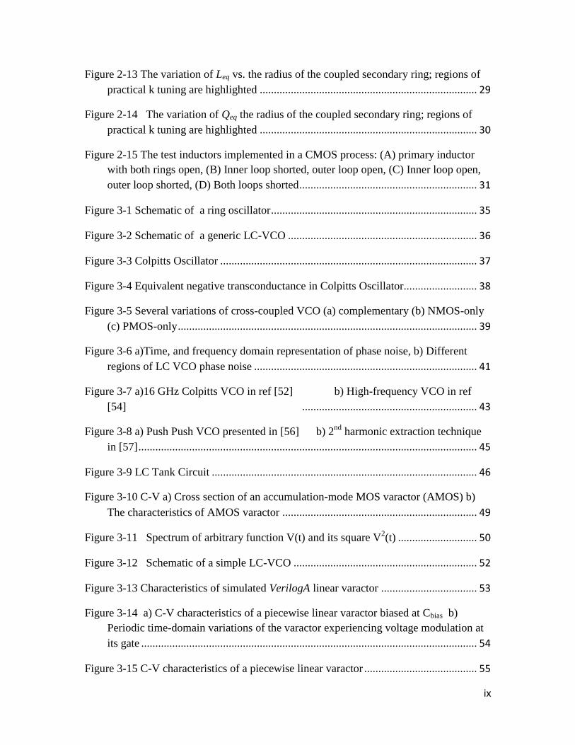
Figure 2-13 The variation of Leq vs. the radius of the coupled secondary ring; regions of
practical k tuning are highlighted ............................................................................. 29
Figure 2-14 The variation of Qeq the radius of the coupled secondary ring; regions of
practical k tuning are highlighted ............................................................................. 30
Figure 2-15 The test inductors implemented in a CMOS process: (A) primary inductor
with both rings open, (B) Inner loop shorted, outer loop open, (C) Inner loop open,
outer loop shorted, (D) Both loops shorted ............................................................... 31
Figure 3-1 Schematic of a ring oscillator ......................................................................... 35
Figure 3-2 Schematic of a generic LC-VCO ................................................................... 36
Figure 3-3 Colpitts Oscillator ........................................................................................... 37
Figure 3-4 Equivalent negative transconductance in Colpitts Oscillator .......................... 38
Figure 3-5 Several variations of cross-coupled VCO (a) complementary (b) NMOS-only
(c) PMOS-only .......................................................................................................... 39
Figure 3-6 a)Time, and frequency domain representation of phase noise, b) Different
regions of LC VCO phase noise ............................................................................... 41
Figure 3-7 a)16 GHz Colpitts VCO in ref [52] b) High-frequency VCO in ref
[54] .............................................................. 43
Figure 3-8 a) Push Push VCO presented in [56] b) 2nd
harmonic extraction technique
in [57] ........................................................................................................................ 45
Figure 3-9 LC Tank Circuit .............................................................................................. 46
Figure 3-10 C-V a) Cross section of an accumulation-mode MOS varactor (AMOS) b)
The characteristics of AMOS varactor ..................................................................... 49
Figure 3-11 Spectrum of arbitrary function V(t) and its square V2(t) ............................ 50
Figure 3-12 Schematic of a simple LC-VCO ................................................................. 52
Figure 3-13 Characteristics of simulated VerilogA linear varactor .................................. 53
Figure 3-14 a) C-V characteristics of a piecewise linear varactor biased at Cbias b)
Periodic time-domain variations of the varactor experiencing voltage modulation at
its gate ....................................................................................................................... 54
Figure 3-15 C-V characteristics of a piecewise linear varactor ........................................ 55

x
Figure 3-16 Comparing the frequency tuning range of analytical expressions and
spectreRF simulations using a VerilogA model for the varactor .............................. 56
Figure 3-17 Comparing the 2nd
harmonic amplitude of analytical expressions and
spectreRF simulations using a VerilogA model ....................................................... 57
Figure 3-18 C-V characteristics for different varactors in CMOS process (W=1.6um,
L=400nm, Multiplier=200) ....................................................................................... 58
Figure 3-19 Schematic of 25 GHz push-push VCO and its output buffers ...................... 60
Figure 3-20 Micrograph of push-push VCO in 90-nm LP CMOS ................................... 60
Figure 3-21 Simulated tuning curve of the 25 GHz push-push VCO vs. the control
voltage ....................................................................................................................... 61
Figure 3-22 Comparison of simulation and measurement results for the tuning curves of
a) Thin-oxide varactor b) Thick-oxide varactor ........................................................ 62
Figure 3-23 Measured output power of the two push-push VCOs when the output buffer
is OFF........................................................................................................................ 63
Figure 3-24 The resonance tank of an LC VCO .............................................................. 65
Figure 3-25 Differential outputs (nodes A & B) of a VCO LC tank carrying fundamental
harmonic fo (in opposite phases) and 2nd harmonic (in-phase). Tank’s Thevenin
equivalent model at the 2nd harmonic is shown on the right. .................................. 66
Figure 3-26 (a) Large buffer transistor means large capacitance modulation that lowers
the 2nd-harmonic swing at node O, (b) Fixed capacitance plus the gate capacitance
of a smaller buffer transistor brings higher resonant swing at node O. .................... 67
Figure 3-27 Schematic of the 25 GHz push-push VCO employing resonance boosting
technique ................................................................................................................... 69
Figure 3-28 Micrograph of the fabricated VCO die in a 90-nm LP CMOS ................... 70
Figure 3-29 (a) Measured frequency tuning range of the push-push VCO, (b) Measured
output power of the VCO with and without the resonance capacitor C1 at node O.
The output buffer was OFF to highlight the amplitude resonance effect. ................ 71
Figure 4-1 a)Two adjacent VCOs coupling to each other b)The current flowing through
the inductor in the aggressor VCO (Ia) generates a voltage on the tank of victim
VCO (Vn,OC) .............................................................................................................. 74

xi
Figure 4-2 A victim VCO oscillates at fo = 4.477 GHz while an aggressor oscillating at fo
+Δf =4.479 GHz induces sidebands at (4.479 GHz – 4.477 GHz) = 2 MHz away
from the victim VCO. Note that the first upper sideband (at the aggressor
frequency) is explained by constructive addition of AM and PM components and is
larger in magnitude than the first lower sideband ..................................................... 76
Figure 4-3 Phasor diagram of AM and PM components in magnetically coupled VCOs 77
Figure 4-4 Closed-loop AC model of a charge-pump based PLL .................................... 78
Figure 4-5 Block diagram of Clock Synthesizer Unit (CSU) ........................................... 79
Figure 4-6 Block diagram of one transceiver link ............................................................ 80
Figure 4-7 Transfer function of the spur generated at the output of PLL ......................... 83
Figure 4-8 Measured total jitter of the victim CSU vs. the offset frequency of aggressor
link ............................................................................................................................ 84
Figure 4-9 Physical view of the single-chip ..................................................................... 86
Figure 4-10 Measured tuning curves of dual LC VCOs across PVT corners .................. 87
Figure 4-11 Closed-loop phase noise and RMS jitter measurement at 1.244 GHz output
(FVCO = 4.976 GHz); RJ=538fs,rms (1 kHz to 40 MHz) using a signal source
analyzer (SSA) .......................................................................................................... 88

xii
List of Abbreviations and Terms
ADC Analog-to-Digital Converter
ADS Agilent Design Systems
AM Amplitude Modulation
AMOS Accumulation-mode MOS varactor
CMOS Complementary Metal-Oxide Semiconductor
CP Charge Pump
CSU Clock Synthesizer Unit
DAC Digital-to-Analog Converter
DNW Deep-Nwell
DSM Deep-Sub-Micron
DUT Device-Under-Test
EHF Extremely-High-Frequency
EM ElectroMagentic
ESD ElectroStatic Discharge
HVT High Vth
IC Integrated Circuit
ISF Impulse Sensitivity Function
LO Local Oscillator
LP-CMOS Low-Power CMOS
LTI Linear Time-Invariant
LTV Linear Time –Variant
MCM Multi-Chip Module
MoM Metal-oxide-Metal
OTN Optical Transport Network
PFD Phase-Frequency Detector
PGS Patterned-Ground Shield
PLL Phase-Locked Loop
PM Phase Modulation
PNA Performance Network Analyzer
ppb parts-per-billion
PVT Process Voltage Temperature
RF Radio Frequency
RJ Random Jitter
RMS Root-Mean-Square
RX Receiver
SERDES Serializer/Deserializer
SiP System-in-Package
SONET Internet Synchronous Optical Networks

xiii
SRF Self Resonance Frequency
SVT Standard Vth
TJ Total Jitter
TX Transmitter
UHF Ultra-High-Frequency
UTM Ultra-Thick-Metal
UWB Ultra-Wide-Band
VCO Voltage Controlled Oscillator
xiv
Acknowledgements
I was very fortunate to enjoy the support of many great people who helped me reach this
milestone in my life. First, I would like to thank my supervisor, Dr. Shahriar Mirabbasi,
for giving me the opportunity to continue working in his research group. Over the past
decade that I enjoyed his supervision and friendship, Dr. Mirabbasi have had an
incredibly positive impact on my life. Both on technical side as well as the personal life,
he taught me many valuable lessons that continue to be my guidelines for the future. He
is literally a true gentleman and a great scientist. I would also like to thank my external
examiner, Dr. S. Stapleton from Simon Fraser University, and my committee members
and university examiners from UBC: Dr. M. Chiao, Dr. E. Cretu, Dr. G. Hinshaw,
Dr. N. Jaeger, and Dr. G. Lemieux, Dr. S. Wilton, and Dr. M. Yedlin for investing their
time to read my thesis and providing me with great comments on different aspects of this
thesis, in particular, Dr. M. Yedlin. who gave me insightful advices on Chapters 1 and 3.
I also would thank Dr. Roberto Rosales for the measurement support and Roozbeh
Mehrabadi for the CAD support.
My sincere gratitude goes to Dr. Hormoz Djahanshahi from PMC-Sierra for many
valuable advices he provided me on the conduct of this research project. His vast
knowledge of analog design, his great personal character and the continuous support he
provided me throughout these years were keys to the success of this research work. I
would also like to thank my great friend, Dr. Farsheed Mahmoudi from Qualcomm for
kindly helping with the VCO design and measurements. I extend my gratitude to George
Deliyannides, Vadim Milirud, Mark Hiebert, and Howard Yang from PMC-Sierra, Dr.
Samad Sheikhaei, and Dr. Pedram Sameni for their valuable technical comments and
assistance on my work.
I cannot express in words my appreciation for what my family has done for me. I was
extremely lucky to have been raised in a family that gave me all the ingredients one needs
to nourish. My late father, Dr. Zabihollah Molavi was my first teacher and taught me the
importance of education. I learned from him that being a human is crystallized in helping
the others and putting the society ahead of myself. It is my honor to dedicate this thesis to
his great soul and his words of wisdom. My mother, Haleh Sadri Tabrizi, is the best gift
xv
sent to me from the heavens. She is the emotional power behind this work that
unconditionally supported me through some harsh days. My Brother, Poorya, showed me
strength and inspired me to be happy and determined. His great engineering knowledge
contributed to the quality of this work. I would like to extend my sincere gratitude to my
dear grandfather Parviz Sadri and also dear uncles and family, Dr. Saifollah Molavi,
Amirghasem Ghasemi Afshar, Ali Reza Sadri, Dr. Marjan and Homa Sadri, Esparnaz
Ghasemi Afshar, Farzaneh Abdollahzadeh, Homayoun Mohazzabfar, Ali and Houtan
Mashinchi, Sasan and Kia Molavi, , Amir Holakoo and Venus Mohazzabfar, and notably
Ali Akbar Seyedfarshi.
Last but not least, to my best friend and companion, Parinaz Tehrani, “Thank You”. You
made my life fun and exciting and kept me motivated to complete this work. Meeting you
is one of the best things that has ever happened to me.
This work was supported in part by the Natural Sciences and Engineering Research
Council of Canada (NSERC), the Canadian Microelectronics Corporation (CMC
Microsystems), and PMC Sierra Inc.
xvi
To the memories of my father
"Modern Human is mindful of the opinion of others; and does not readily rule out others
ideas even if they are in contrast with her/his own views "
1
Chapter 1
Introduction
The ever-increasing demand for high-speed communication has produced enormous
interest for the deployment of microwave and mm-wave portion of the frequency
spectrum [1][2]. The deployment of the radio spectrum from 3 to 10 GHz in ultra-wide-
band (UWB) technology has enabled high-bandwidth wireless communications at very
low energy levels for short-range applications [3][4]. To facilitate the use of wideband
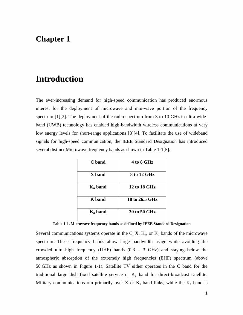
signals for high-speed communication, the IEEE Standard Designation has introduced
several distinct Microwave frequency bands as shown in Table 1-1[5].
C band 4 to 8 GHz
X band 8 to 12 GHz
Ku band 12 to 18 GHz
K band 18 to 26.5 GHz
Ka band 30 to 50 GHz
Table 1-1. Microwave frequency bands as defined by IEEE Standard Designation
Several communications systems operate in the C, X, Ka, or Ku bands of the microwave
spectrum. These frequency bands allow large bandwidth usage while avoiding the
crowded ultra-high frequency (UHF) bands (0.3 – 3 GHz) and staying below the
atmospheric absorption of the extremely high frequencies (EHF) spectrum (above
50 GHz as shown in Figure 1-1). Satellite TV either operates in the C band for the
traditional large dish fixed satellite service or Ku band for direct-broadcast satellite.
Military communications run primarily over X or Ku-band links, while the Ka band is
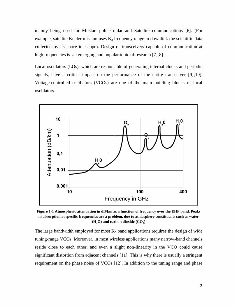
2
mainly being used for Milstar, police radar and Satellite communications [6]. (For
example, satellite Kepler mission uses Ka frequency range to downlink the scientific data
collected by its space telescope). Design of transceivers capable of communication at
high frequencies is an emerging and popular topic of research [7][8].
Local oscillators (LOs), which are responsible of generating internal clocks and periodic
signals, have a critical impact on the performance of the entire transceiver [9][10].
Voltage-controlled oscillators (VCOs) are one of the main building blocks of local
oscillators.
Frequency in GHz
Atte
nu
atio
n (
dB
/km
)
Figure 1-1 Atmospheric attenuation in dB/km as a function of frequency over the EHF band. Peaks
in absorption at specific frequencies are a problem, due to atmosphere constituents such as water
(H2O) and carbon dioxide (CO2)
The large bandwidth employed for most K- band applications requires the design of wide
tuning-range VCOs. Moreover, in most wireless applications many narrow-band channels
reside close to each other, and even a slight non-linearity in the VCO could cause
significant distortion from adjacent channels [11]. This is why there is usually a stringent
requirement on the phase noise of VCOs [12]. In addition to the tuning range and phase
3
noise, several other requirements such as power consumption, oscillation amplitude, and
die area have to be diligently considered in a VCO design.
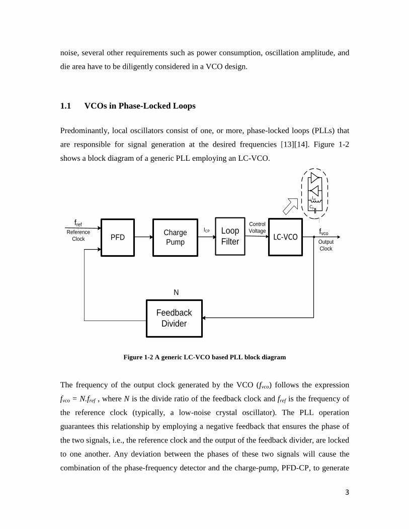
1.1 VCOs in Phase-Locked Loops
Predominantly, local oscillators consist of one, or more, phase-locked loops (PLLs) that
are responsible for signal generation at the desired frequencies [13][14]. Figure 1-2
shows a block diagram of a generic PLL employing an LC-VCO.
PFDCharge
Pump
Loop
Filter
Feedback
Divider
LC-VCOOutput
Clock
Lp
Cp
Reference
Clock
N
Control
VoltageICP
fref
fvco
Figure 1-2 A generic LC-VCO based PLL block diagram
The frequency of the output clock generated by the VCO (fvco) follows the expression
fvco = N.fref , where N is the divide ratio of the feedback clock and fref is the frequency of
the reference clock (typically, a low-noise crystal oscillator). The PLL operation
guarantees this relationship by employing a negative feedback that ensures the phase of
the two signals, i.e., the reference clock and the output of the feedback divider, are locked
to one another. Any deviation between the phases of these two signals will cause the
combination of the phase-frequency detector and the charge-pump, PFD-CP, to generate

4
a corrective current pulse (ICP in Figure 1-2) into the loop filter [15]. This current
modulates the loop filter output voltage that, in turn, varies the frequency of the VCO
(output clock). Corrected VCO phase may be divided down through the optional
feedback divider, eventually forcing PFD to respond, accordingly.
The design of VCO as the main block responsible for the clock generation is of
pronounced importance for a proper PLL operation. The generic LC-VCO shown in
Figure 1-2 (inset) is a simplified model of an LC-VCO which we will return to in
Chapter 3. It consists of an active circuitry and an LC tank. The study of properties and
characteristics of LC components and their impact on the performance of LC-VCOs
constitutes the basis of this dissertation.
1.2 CMOS Implementation Challenges
Traditionally, the design of RF transceivers entailed a challenging integration problem.
To achieve high performance, some critical RF and analog circuitry are still being
implemented in silicon-germanium (SiGe) or gallium-arsenide (GaAs) technologies. On
the other hand, most base-band and mixed-signal components, e.g., digital-to-analog
converters (DACs), analog-to-digital converters (ADCs), and digital signal processing
blocks (DSPs) are being fabricated in a complementary metal-oxide semiconductor
(CMOS) technology. Furthermore, implementing high quality passive filters could
require the usage of discrete components. Hence, most commercial RF transceivers had
to adopt a multi-chip module (MCM) or system-in-package (SiP) solution to integrate
most of the components resulting in an increase in the cost [16][17].
The incredible growth of the digital processes in recent years, mostly due to the
continuous scaling in CMOS technology, has motivated designers to develop CMOS
analog components for various applications and facilitating a single-chip solution.
Furthermore, the transit frequency (ft) of MOS devices has dramatically increased due to
the evolution of deep-sub-micron (DSM) technologies (ft’s exceeding 100's of GHz)
enabling design of high-speed analog and RF circuit in CMOS.
Rapid advancements in RF CMOS design were further accelerated through the evolution
of high-quality passive components on silicon substrate. As mentioned earlier, integrated
5
inductors are one of the critical constituents of the state-of-the-art CMOS LC VCOs
[18-20]. Spiral inductors started to appear in the mixed-signal CMOS designs in the late
90s [19][20]. Originally, the modeling process of inductors for analog CMOS design was
relatively time-consuming and required specific custom-developed tools such as ASITIC
and ADS Momentum with moderate accuracies [21][22]. The accuracy of these tools
would also depend on the type and complexity of subject structures. For example, ADS
Momentum, as a 2.5-D simulation tool, uses pre-computed functions to simplify the
electromagnetic simulation from 3-dimensions to 2-dimensions, and may pose modeling
constraints if employed to compute the inductance for 3-D structure with several metal
layers. Recently, a number of commercial tools such as Helic, SONNET and Integrand
have emerged that feature inductor pcells (custom-made layout cells with parameterized
properties) and are conveniently built into the mainstream design tools such as Cadence
Virtuoso [23][24]. However, the relatively high cost, licensing issues, significant
simulation time (required to model custom structures) and lack of analytical data limited
their usage in research environments. The current trend towards using non-traditional
inductor structures such as helical inductors and coupled rings in integrated circuit (IC)
design, and the need for reliable models and analytical expressions to predict their
performance metrics are the driving forces for our study of integrated passive inductors.
The design of inductors in a mixed-signal chip may get further complicated if several
spiral inductors are integrated close to one another. A common example is the integration
of several LC-VCO-based PLLs on a single Serializer/Deserializer (SERDES) chip (for
wireline communication) [25]. The coupling effect amongst these VCOs, also a subject of
our study, may result in unwanted interactions between neighboring circuits and
adversely impact their performance.
The implementation of LC-VCOs in CMOS also benefits from the use of accumulation-
mode variable capacitors, also known as AMOS varactors, employed to tune the VCO
frequency. Commonly referred to as "NMOS in n-well", this implementation of MOS
device never enters into inversion regime [26], therefore, exhibiting a monotonic
characteristic, as discussed in detail in Chapter 3. Despite several years of use in LC-
VCO oscillators, the different impacts of AMOS varactors on the performance of the
6
VCO, are still being investigated. Several researchers have elaborated on the effects of
these devices on the frequency tuning range of VCOs [27][28]. However, the complexity
of the respective mathematical equations has impeded the development of a complete set
of analytical solutions. Following few simplifying assumptions, this thesis derives the
mathematical expressions relating the properties of AMOS varactor to the frequency
tuning range and amplitude of output harmonics. These expressions provide design
insights and intuitions as how to employ varactor non-linearity to operate the LC-VCOs
for frequency synthesis at higher harmonics of the fundamental frequency. Using these
guidelines, the design of a push-push (second-order harmonic VCOs) is presented.
1.3 Contributions
The objective of this dissertation is to present solutions at the device, circuit, and system
levels for a key circuit building block, namely, LC-VCO, that is almost ubiquitously
employed in integrated transceivers, as well as other communication and computing
devices. The proposed solutions for LC-VCOs are useful in any PLL-based system
employing one such oscillator. Hence, the solutions are either directly or indirectly
applicable to other systems that incorporate PLL circuits such as clock and data recovery
(CDR) systems. Key contributions of this work are as follows:
1.3.1 Analytical and Device-Level Models for Several Inductor Structures
In this work, we have studied different structures of passive inductors such as doubly-
stacked inductors, vertical inductors, and coupled-rings (a popular structure for variable
passive inductors) from a circuit perspective. We have thus developed circuit models to
accurately estimate the inductance and quality factor of these structures. The analytical
expressions proposed in this work provide designers with a reasonable estimate of their
circuit performance and layout constraints. This information is of great value to RF
system designers who are involved in the block specifications and floor-planing of the
entire chip. The result of proposed analyses are verified by the measurement results of
two test structures implemented in two different CMOS processes.
7
1.3.2 Second Harmonic Analysis and Amplification in Push-Push LC VCOs
We have studied the effect of large signals on the LC-VCOs by developing a
mathematical model to solve the non-linear differential equation governing the LC tank
circuit (in both the small-signal and large-signal regimes). The study shows that the VCO
frequency is a function of the amplitude of the higher-order harmonics of the output
voltage. It is also shown that amplitude of higher harmonics of the output voltage is a
function of circuit parameters such as the C-V characteristics of the varactor and the
output signal amplitude. Hence, it is proposed that an LC-VCO employing center-tapped
inductor can extract and amplify this second-harmonic. This design proves useful for
high-frequency applications and maximizes the frequency tuning range. Based on t he
proposed architecture, a K-band VCO is designed, simulated, fabricated, and successfully
tested.
Also, a low-power technique to boost the output amplitude of push-push VCOs is
introduced. It is shown that a resonance effect created by the insertion of a second
varactor, tuned in harmonious with the tank varactor, significantly increases the
amplitude of the second-harmonic output. Measurement results of a proof-of-concept
prototype test chip confirm the usefulness of the proposed technique .
1.3.3 Coupling Analysis for Densely Integrated PLLs
This work presents an analytical model to study the effect of coupling between adjacent
LC VCOs closely integrated on the same chip. This model explains the existence of
spurious sidebands as observed in the frequency spectrum of two (or more) closely-
running adjacent links. A redundant frequency mapping scheme is proposed that reduces
this coupling effect by up to 12 dB. Measurement results of a highly packable clock
synthesizer in a 65-nm CMOS technology confirm the validity of the analytical model
and the effectiveness of the proposed mapping technique.
8
1.4 Organization of Thesis
In Chapter 2, we study several structures of fixed and variable inductors. To compare the
performance of different structures, three passive inductors are modeled and designed in
65-nm CMOS. Using EM simulations, measurement results, and performance
comparison of these structures, a unified circuit model is proposed for the self-inductance
of the different spiral designs. Next, we turn our attention to the structures of variable
inductors, in particular, coupled rings. This efficient structure of variable inductors is
analyzed from a design point of view and analytical expressions are developed to
estimate the different metrics of the inductor. Finally, the simulations and measurement
results of test structures in 65-nm CMOS are presented and compared with the analytical
results.
Chapter 3 reviews several recent architectures for high-frequency LC-VCOs. From this
study, it is suggested that push-push VCOs, employing the second-harmonic of the
oscillation, are suitable for wide-tuning-range high-frequency designs. To establish the
basis of second-harmonic generation in LC VCOs employing AMOS varactors, an
analytical framework is developed. Based on the results of this analysis, circuit-level
solutions are proposed to boost the amplitude of push-push LC-VCOs. The measurement
results of a proof-of-concept prototype LC-VCO in 90-nm CMOS, designed based on the
proposed technique, are presented.
Chapter 4 presents the coupling issues facing the dense integration of several LC-VCOs
on a single chip. The coupling effect in LC-VCO-based PLLs is studied from an
analytical perspective and is accompanied by measurement results.
Finally, the concluding remarks and future research avenues are presented in Chapter 5.
9
Chapter 2
Analysis, Design, Simulation and Verification
of Integrated Inductors in Bulk CMOS
Monolithic inductors are commonly used in state-of-the-art high-speed analog, mixed-
signal, and radio-frequency (RF) integrated circuits. The performance of these circuits
depends on the inductance (L) and quality factor (Q) of such passive inductors. Since
monolithic inductors are implemented on lossy silicon substrate in a CMOS technology,
they typically have a poor quality factor, which leads to degradations in circuit efficacy,
especially at RF and microwave frequencies.
In particular, passive components, including inductors and transformers, are extensively
used in communication circuits for both wireless and wireline applications. Examples of
these circuits include LC-oscillators, which demand a good phase noise performance to
meet the stringent requirements of wireline and wireless communication standards,
inductive load of amplifiers and mixers to improve their respective gain, and inductor-
based matching circuits in wireless and wireline transceivers to extend the operation
bandwidth of transmit and receive circuits. The trend toward higher levels of integration
in deep-sub-micron (DSM) CMOS designs (e.g. 65-nm, 40-nm and beyond), tends to
lower inductor quality factor due to closer proximity of the top metal layers to the
substrate, and reduced thickness and hence increased resistance of the metal layers
available in the stack. A recent DSM option, the ultra-thick-metal (UTM) with lower
resistivity [29], ameliorates the resistance effect, however, there is an extra
10
manufacturing cost associated with using this option and it may only be available in
selected processes. Given the available technology options and trade-offs between
inductance, area, Q, and self-resonance frequency (SRF) of the inductor, an accurate EM
field simulator capable of modeling all DSM effects for various 3D structures, becomes
an essential ingredient for today’s integrated circuit design.
Our intention in this chapter is to study and analyze several structures of fixed and
variable inductors. First, the design of several fixed inductor structures in CMOS process
is discussed. To compare the performance of different structures, three passive inductors
are designed. The modeling technique, EM simulations, measurement results, and
performance comparison of these three structures are discussed in detail. Next, the design
of coupled rings structures are studied from an analytical perspective. In order to verify
the results of the proposed analysis, several coupled rings are designed and simulated.
Measurement results of the coupled ring test structures implemented in CMOS show
good agreement with the proposed analysis.
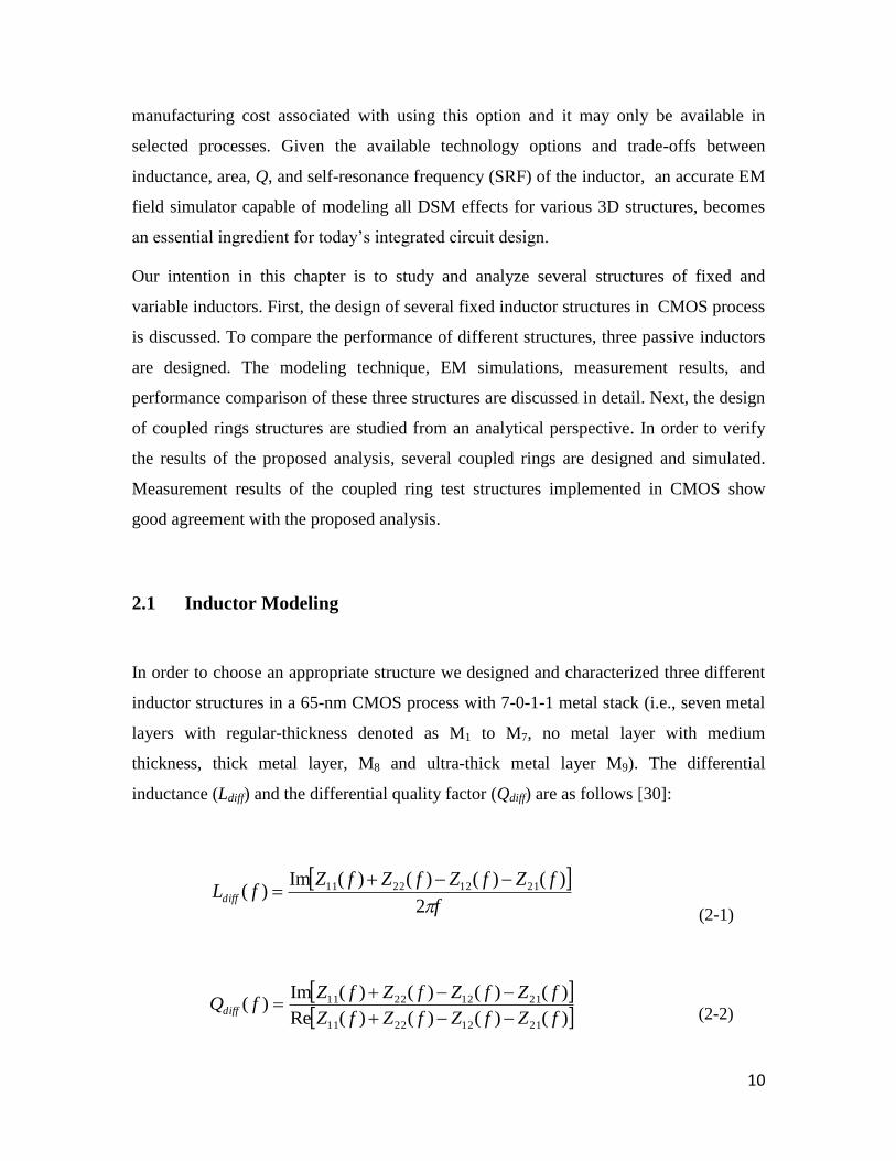
2.1 Inductor Modeling
In order to choose an appropriate structure we designed and characterized three different
inductor structures in a 65-nm CMOS process with 7-0-1-1 metal stack (i.e., seven metal
layers with regular-thickness denoted as M1 to M7, no metal layer with medium
thickness, thick metal layer, M8 and ultra-thick metal layer M9). The differential
inductance (Ldiff) and the differential quality factor (Qdiff) are as follows [30]:
f
fZfZfZfZfLdiff
2
)()()()(Im)( 21122211
( 2-1)
)()()()(Re
)()()()(Im)(
21122211
21122211
fZfZfZfZ
fZfZfZfZfQdiff
( 2-2)

11
Metal Width (W) Turns (N) Metal Spacing (S) Outer Diameters
Inductors (a), (b) 9μm 2 3μm 112μm 102μm
Inductor (c) 9μm 1 3μm 78μm 78μm
Table 2-1 Physical dimensions of the implemented inductors
(a)
(b)
(c)
(
Figure 2-1 The test inductors implemented in a 65-nm CMOS process (a) 2-turn lateral top-metal
inductor (b) 2-turn lateral doubly-stacked inductor (c) 2-turn vertical inductor
In this work, we focus on three commonly used structures that are used in high-frequency
applications. Shown in Figure 2-1, these three structures are:
(a) Two-turn single-layer lateral inductor in the top metal layer (M9); underpass on M8,
(b) Two-turn lateral doubly-stacked inductor (two parallel metal layers (ultra-thick M9
and thick M8) connected with many vias throughout); underpass on M7 and M6,
(c) Two-turn two-layer vertical (a.k.a. helical) inductor.
As shown in the Figure 2-1, structures (a) and (b) appear similar from a top view point
due to their equal metal width (W) and spiral dimensions (outer diameter and inter-
winding spacing, S). However, due to the addition of M8 layer in structure (b), the values
of Ldiff and Qdiff will slightly be different.
12
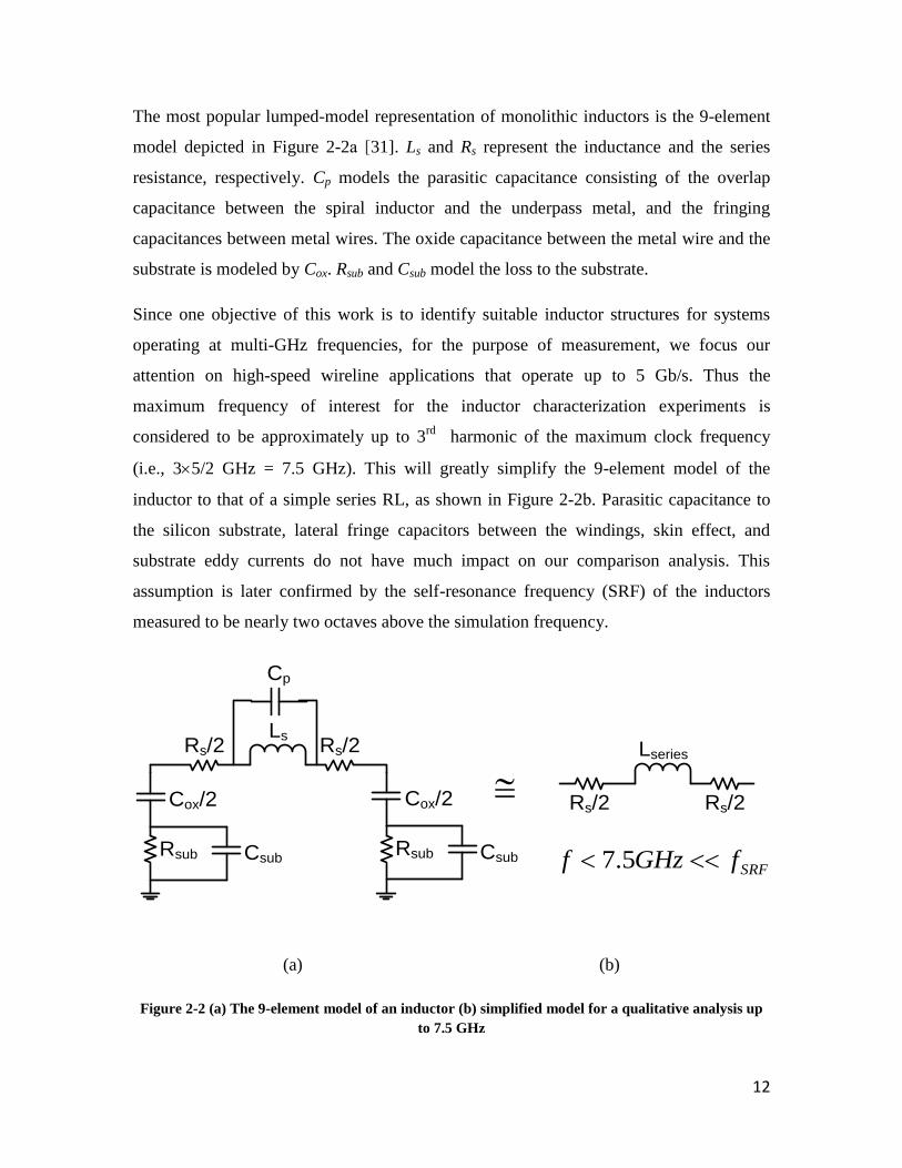
The most popular lumped-model representation of monolithic inductors is the 9-element
model depicted in Figure 2-2a [31]. Ls and Rs represent the inductance and the series
resistance, respectively. Cp models the parasitic capacitance consisting of the overlap
capacitance between the spiral inductor and the underpass metal, and the fringing
capacitances between metal wires. The oxide capacitance between the metal wire and the
substrate is modeled by Cox. Rsub and Csub model the loss to the substrate.
Since one objective of this work is to identify suitable inductor structures for systems
operating at multi-GHz frequencies, for the purpose of measurement, we focus our
attention on high-speed wireline applications that operate up to 5 Gb/s. Thus the
maximum frequency of interest for the inductor characterization experiments is
considered to be approximately up to 3rd
harmonic of the maximum clock frequency
(i.e., 35/2 GHz = 7.5 GHz). This will greatly simplify the 9-element model of the
inductor to that of a simple series RL, as shown in Figure 2-2b. Parasitic capacitance to
the silicon substrate, lateral fringe capacitors between the windings, skin effect, and
substrate eddy currents do not have much impact on our comparison analysis. This
assumption is later confirmed by the self-resonance frequency (SRF) of the inductors
measured to be nearly two octaves above the simulation frequency.
Rsub
Cox/2
Csub
Ls
Rsub
Cox/2
Csub
Cp
Rs/2
Lseries
SRFfGHzf 5.7
Rs/2 Rs/2
Rs/2
(a) (b)
Figure 2-2 (a) The 9-element model of an inductor (b) simplified model for a qualitative analysis up
to 7.5 GHz
13
Lk
LLk
LLk
MLMLL
eq
eq
eq
)2
1(1
1
111
21
)1(21
41
21
kLLk
LLk
MLMLL
eq
eq
eq
L1 M
L2 M
L1 M L2 M
L
21
21
LLkM
LLL
(a)
(b)
(c)
Figure 2-3 Equivalent inductance calculations for the three implemented structures corresponding to
those in Figure 2-1
The inclusion of M8 in the inductor structure (b) is equivalent to increasing the cross-
section area of the inductor wires approximately by the thickness of this metal layer. In
the technology used here, the top two metal layers (M9 and M8) have a thickness ratio
(TR) of 3.8. Therefore, one expects the series resistance (RS) in Figure 2-2(b) to reduce
by 1−(3.8/4.8) ≈ 21% when stacking the two layers in parallel. This estimate is confirmed
by Momentum simulations showing RS to drop from 1.9 Ω to 1.5 Ω.
This effect also manifests itself as a proportional increase in the quality factor of the
combination stack; in this case the simulated Qdiff increased from 8.7 to 10.6, i.e., a 22%
increase verifying the earlier calculations. The value of inductance also changes due to
the change in the current density in each turn of the inductor. It can be shown that for a
compact inductor with large ratio of the spiral inner radius, r, to the cross-section radius
of the wire a (i.e., the ratio a
r), the inductance value can be approximated as [32]:

14
2)
8ln(0
a
rrL
( 2-3)
This means that a change in the cross-section of the inductor wire by going from an
effective cross-section radius a1 to a2 causes a small change in the inductance calculated
by:
)ln(
2
10
a
arL
( 2-4)
Going from single-layer to doubly-stacked a2 > a1, hence ΔL ≤ 0, i.e. the inductance
slightly decreases. Substituting for TR = 3.8 translates to 10 to 20 pH change in the
inductance depending on the approximations used to define effective cross section radius.
(Note the simulated and measured ΔL= La – Lb of 23 pH in Table 2-2. From the circuit
perspective, this can be visualized as shown in Figure 2-3. The equivalent inductance for
structure (b) which is the case of two highly-coupled parallel inductors remains slightly
smaller than each individual one, as shown in Figure 2-3b.
Ldiff (5 GHz) Qdiff (5 GHz) RDC (Ω) Qmax
Inductor (a) 511pH 8.7 1.8 12.7
Inductor (b) 488pH 10.6 1.42 12.5
Inductor (c) 490pH 9.4 1.61 11.8
Table 2-2 Simulation results of all three inductor structures
Immediately, the advantage of the structure (c) becomes apparent from Figure 2-3C.
Employing two highly-coupled series inductors, which is the property of the helical
structure (c), results in an equivalent inductance nearly four times larger than each one of
them. In fact, it can be shown that Leq for helical inductors is proportional to m2 where m
is the number of vertical turns. Therefore, one can achieve large inductances with much
smaller lateral dimensions hence saving area. Based on the above, doubly-stacked
structures appear to offer a reasonable trade-off among inductance, area and the quality
factor.
15
The structure (c), as shown in Figure 2-1, is physically smaller than the other two
structures and relies on the vertical concentration of flux to achieve similar values of
inductance as in structures (a) and (b). Since one turn is implemented in a lower metal
layer, M8, that is more resistive and comes in series with the top layer, it is predicted that
this type of inductor will not offer higher values of Q, in low to medium range
frequencies where substrate losses are still small.
However, such structure may well be attractive for applications where a large value of
inductance is required, e.g. bandwidth extension by inductive peaking. Constructing
several turns that are vertically stacked in series is achievable in multi-metal layer DSM
technologies (state-of-the-art processes have up to 10 metal layers). Also, since
Momentum is a 2.5-D EM simulator, the comparison between EM simulation and on-
wafer S-parameter measurements allows us to verify the ability and quantify the accuracy
of this design suite to model 3-D structures. Table 2-2 summarizes simulation results of
all three inductors. In this table, the parameter Qmax, maximum quality factor across the
frequency, indicates that the slight degradation in SRF for structures (b) and (c) can be
attributed to the inclusion of the lower metal layers.
2.2 Measurement Results of Fixed Inductors
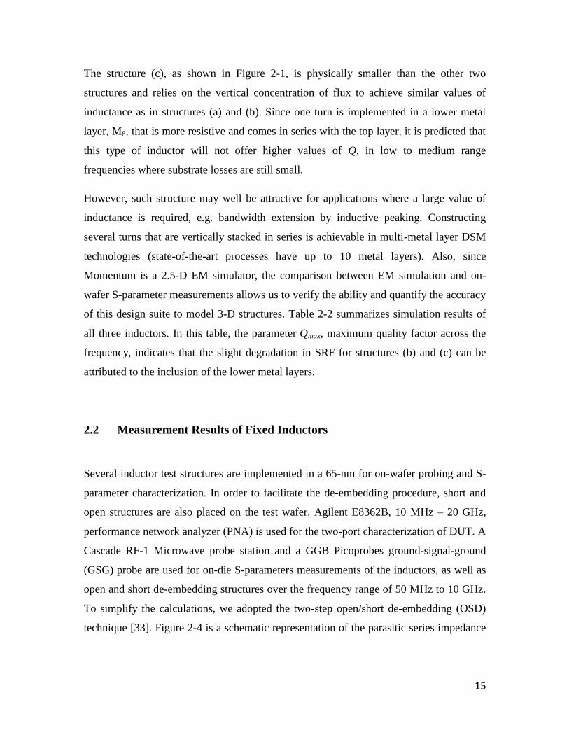
Several inductor test structures are implemented in a 65-nm for on-wafer probing and S-
parameter characterization. In order to facilitate the de-embedding procedure, short and
open structures are also placed on the test wafer. Agilent E8362B, 10 MHz – 20 GHz,
performance network analyzer (PNA) is used for the two-port characterization of DUT. A
Cascade RF-1 Microwave probe station and a GGB Picoprobes ground-signal-ground
(GSG) probe are used for on-die S-parameters measurements of the inductors, as well as
open and short de-embedding structures over the frequency range of 50 MHz to 10 GHz.
To simplify the calculations, we adopted the two-step open/short de-embedding (OSD)
technique [33]. Figure 2-4 is a schematic representation of the parasitic series impedance
16
and shunt admittance of interconnect leads and pads, respectively.
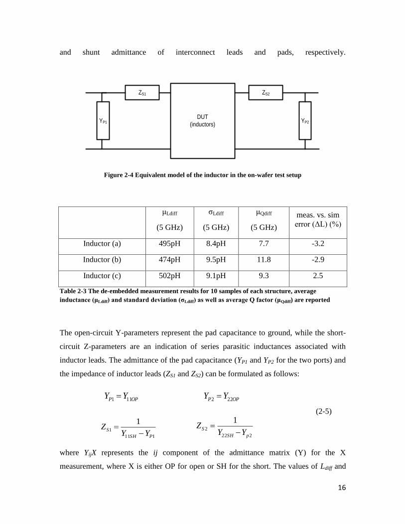
DUT
(inductors)
ZS2
YP2
ZS1
YP1
Figure 2-4 Equivalent model of the inductor in the on-wafer test setup
μLdiff
(5 GHz)
σLdiff
(5 GHz)
μQdiff
(5 GHz)
meas. vs. sim
error (ΔL) (%)
Inductor (a) 495pH 8.4pH 7.7 -3.2
Inductor (b) 474pH 9.5pH 11.8 -2.9
Inductor (c) 502pH 9.1pH 9.3 2.5
Table 2-3 The de-embedded measurement results for 10 samples of each structure, average
inductance(μLdiff)andstandarddeviation(σLdiff)aswellasaverageQfactor(μQdiff) are reported
The open-circuit Y-parameters represent the pad capacitance to ground, while the short-
circuit Z-parameters are an indication of series parasitic inductances associated with
inductor leads. The admittance of the pad capacitance (YP1 and YP2 for the two ports) and
the impedance of inductor leads (ZS1 and ZS2) can be formulated as follows:
OPP YY 111 OPP YY 222
111
1
1
PSH
SYY
Z
222
2
1
pSH
SYY
Z
( 2-5)
where YijX represents the ij component of the admittance matrix (Y) for the X
measurement, where X is either OP for open or SH for the short. The values of Ldiff and
17
Qdiff are calculated using ( 2-1) and ( 2-1) and are summarized in Table 2-3. As can be
seen, the measurement results are in a close agreement with the simulation results of
Table 2-2, and there exists a small systematic error for lateral structures (a) and (b),
which is different for the vertical structure (c) (≈ -3% versus. +2.5%). In the next section
these results are used to design a dense inductor to enhance the bandwidth at the input of
an impedance-matched amplifier.
2.3 Vertical Inductor for Series Peaking
Figure 2-5(a) shows the equivalent model of a 50 Ω-matched amplifier running at up to
5.4 Gbps. The model includes the parasitic capacitances of the electrostatic discharge
(ESD) structures, as well as those of the pad. A resistance of value of 100 Ω (Resd) is
inserted in the signal path to limit an ESD-event current. Rterm and Cin represent the
termination resistance and amplifier input capacitance, respectively.
RtermCpad
Resd
Cesd Cin
PADA
(a)
75mVpp
(b)
Figure 2-5 (a) Schematic model for the input of an impedance-terminated receiver (b) Eye-diagram
at point (A)

18
(a)
RtermCpad
ResdCesd Cin
PADLseries
A
(b)
115mVpp
Figure 2-6 (a) Inclusion of series-peaking at the input of amplifier (b) The improved eye-diagram at
point (A)
The signal received at internal point A, suffers from substantial loss due to the board
traces, package impedances and ESD structures. The received signal eye diagram for
a transmitted signal of 1 Vpp and 10 inches of FR4 trace is depicted in Figure 2-5b. As can
be seen, the vertical eye-opening is fairly small (75 mVpp) hence the amplifier input
may not be able to recover the input data correctly.
Bandwidth extension using series-peaking is an attractive technique to boost the data
eye-opening at this interface [34]. As illustrated in Figure 2-6a, a 4.7 nH inductor is
placed in series with Resd. Based on the corresponding simulated eye-diagram shown in
Figure 2-6 (b), the vertical opening in the middle of the eye has been improved by 50% to
115 mVpp at 5 Gbps. A 4.7 nH inductor can occupy a large area if implemented as a
lateral structure, such as structures (a) or (b) in Section 2.1. However, since this inductor
19
is in series with Resd, it can tolerate a low Q and hence its resistance can be absorbed into
that of the ESD structure. An implementation that particularly benefits from this
approach is the compact vertical inductor (structure “c”) described earlier. An
approximate formula for the inductance of spiral inductors is given by rn2
0 [32]
where r and n are average spiral radius and number of lateral turns, respectively.
Combining these with the findings of Section 2, we modify the approximate formula
for a helical inductor as
rnmL 22
0 ( 2-6)
where m represents the number of vertical turns. Using n = 4 and m = 3, as illustrated in
Figure 2-7, r is calculated to be ≈ 25 μm to produce 4.7 nH of inductance. Momentum
simulations show a compact 3-turn helical inductor with r = 22.5 μm achieves an
inductance of 4.7 nH and a resistance of 30 Ω. In practice, in the series-peaking network
shown in Figure 2-6 (a), Resd is trimmed down accordingly by 30 Ω to absorb RS of the
structure. To save process cost, this inductor does not use UTM option and the top two
metal layers are default thick metals instead, i.e. M9 and M8. The bottom windings are
made of the parallel connection of thin metal layers M6-M7, analogous to the structure (b)
in Figure 2-1 to mitigate large series resistance of thin metal layers.
(a)
M8
M7M6
M9
(b)
Figure 2-7 The vertical inductor designed for series peaking (a) Top-view (b) Lateral view
20
2.4 Variable Inductors
The most dominant application of integrated inductors is in the “tuned circuits” where
one is interested in generating or amplifying signals from a certain band(s) of frequency
spectrum while suppressing frequency components outside that band. The series-peaking
design in the previous section is an example of tuned-circuit for bandwidth enhancement.
The increasing number of wireless and wireline standards and the need for modern
electronic devices to support multitude of these standards has made wideband and
programmable tuned circuits more attractive. Varactors and switched-capacitor have
extensively been used in the electronic circuits in response to this demand. However, as
the operating frequency of tuned-circuits enters the microwave range, a number of issues
limit their usability. To elaborate, consider a simple tuned LC network as shown in
Figure 2-8(a).
A
B
RSC
C
A
B
L
RSL
C L RP
(a) (b)
Figure 2-8 (a) A lossy tuned LC circuit (b) The parallel equivalent circuit
Resistors RSC and RSL model the equivalent series loss of the capacitor and the inductor,
respectively. As shown in Figure 2-8 (b), it is straightforward to show that these losses
can be combined into a parallel component given by:
21
)1
()()()(22
2222
SCSL
SCCSLLpRCR
LRQRQR
( 2-7)
RP determines the overall quality factor of the tuned circuit and is usually kept high to
minimize the noise and power consumption of the circuit. The value of Rp in the low
frequencies is dominated by the first component, i.e. the inductive loss term, 2L
2/RSL,
while at higher frequencies the capacitive component 1/(2L
2Rsc) becomes the dominant
contributor. Also recall that the tunability of a passive component usually comes at the
cost of compromised quality factor, making tunable capacitors less desirable when their
loss dominates that of the tank. Thus, at high frequencies, where the impact of inductor
loss is less evident, the viability of employing variable inductors, as an alternative option
to extend the tuning range, grows.
Different techniques have been proposed in literature to construct variable passive
inductors either by self-inductance switching [35-36] or mutual-inductance coupling
switching [37-39]. The latter approach is more attractive since the loss of the switching
component affects the performance to a smaller extent [37]. Figure 2-9 (a) shows the
basic idea of mutual-coupling switching where a switch (SW in Figure 2-9 (a)) is inserted
in the secondary path of two mutually-coupled inductors. When the switch is in OFF
state, there is no current flowing through the secondary winding and the inductance
looking into the input of the primary winding is approximately L1. However, when the
switch is in ON state, according to Lenz’s law, the current in the primary winding,
induces a current in the secondary that, in turn, opposes the original magnetic flux.
Therefore, the net magnetic flux through the main loop (primary) is smaller, hence the
equivalent inductance is smaller. Note that the change in the inductance comes at the cost
of translating the output impedance of the secondary winding, i.e., the series loss of L2
plus the impedance of the switch, to the primary.

22
M
SW
L1
R1
L2
R2
ZSW
M
+
-
V
I
I
+-
Zin
Leq
Req
+
-
(a)
(b) (c)
Zin
L1,Q1
L2,Q2
Figure 2-9 (a) Two octagonal spirals configured as coupled rings, (b) The equivalent circuit, (c)
Simplified model
This translated impedance is effectively in series with the loss of primary winding and
degrades the overall quality factor. The magnitude of translated impedance, as well as the
net change in the value of inductance, is a function of the magnetic coupling between the
two windings. This creates a subtle trade-off between the tunability of the coupled-
inductors and their quality (factor). To analytically demonstrate the trade-off, consider
the equivalent model of two coupled rings as shown in Figure 2-9 (b). It is
straightforward to show that the input impedance of this circuit is given by:
SW
inZLjR
MLjRZ
12
22
11)(
( 2-8)
23
where M and ZSW represent the mutual inductance and the switch impedance,
respectively. Assuming ZSW ≈ RSW, and modeling the input impedance with a lossy
inductor (Leq, and Req as shown in Figure 2-9 (c)), the equivalent inductance is:
)1()1(
)(
2
1
21
2
1
2
2
22
2
2
22
1
kLLL
ML
LRR
LMLL
SW
eq
( 2-9)
where the assumption made here is that the quality factor of the secondary winding is
sufficiently high (Q2 >> 3). Similarly, we can show that:
)(
)(
)(
22
2
2
1
2
2
22
2
2
22
1
SW
SW
SWeq
RRL
MR
LRR
RRMRR
( 2-10)
The last term in Eq. (10) can be re-written as:
).1(
).)(
.1(
2
12
1
1
1
2
2
12
2
1
Q
QkR
R
L
L
RR
LL
MRR SW
eq
( 2-11)
Hence, we calculate the quality factor of the variable inductor as:
2
12
2
1
2
12
1
2
1
.1
1.
).1(
)1(
Q
Qk
kQ
Q
QkR
kL
R
LQ
eq
eq
eq
( 2-12)
The significance of (2-12) is that it emphasizes that the equivalent quality factor is
independent of the value of the secondary inductance L2, and only depends on the
secondary inductor’s quality factor and its coupling to the primary. The ratio 21 QQ in the
denominator of (2-12) should be kept small to improve the quality factor Qeq. The main
24
inductor, i.e. L1, is typically implemented with top thick metal layers, and this poses a
challenge to make smaller than unity. Also, consider that RSW is in the series path
of the secondary inductor and should be made negligible compared to R2 to avoid
degrading Q2. Hence setting a good design target as 121 QQ , we can arrive at the
following:
2
2
1
2
11
1.),1(
k
kQQkLL eqeq
( 2-13)
Note that while these results were derived for two coupled inductors, they also equally
apply to coupling effect from other low-loss metallic structures to any inductor. For
example, (2-12) can be used to predict the performance degradation for a particular
inductor due to the vicinity to other nearby metallic structures.
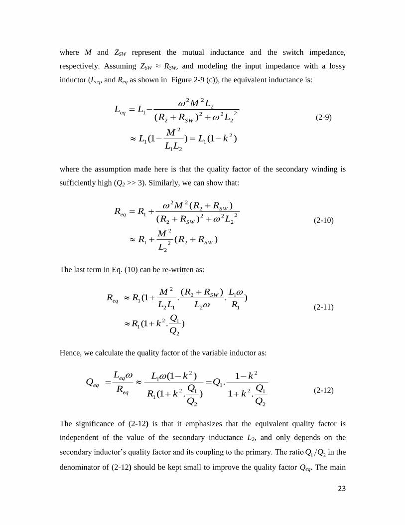
Figure 2-10 depicts the plot of Leq and Qeq vs. the coupling factor k from (2-13) As can be
seen, there is only a small range of k values for which this structure produces useful
results. For k < 0.2, the resulting change in the inductance is less than 4%, which is a
typical margin of error in the inductor modeling. As k increases above 0.2, this structure
produces tangible changes in the value of Leq at the cost of Qeq degradation. However, for
k > 0.55, there is over 50% loss in the quality factor of the inductor, which translates to
about 3 dB signal-to-noise degradation in the system. This may not be tolerable in high-
performance applications, hence for most practical applications coupled rings with 0.2 <
k < 0.55 are desirable.
25
Figure 2-10 The variation of Leq and Qeq vs. the coupling factor (k)
With all its simplicity, (2-13) introduces a new variable, k, to a designer who seeks to
optimize Leq and Qeq for a particular application. In order to relate k to the circuit
parameters, we need to calculate L1, L2 and M for two coupled rings and substitute in
21LLMk .
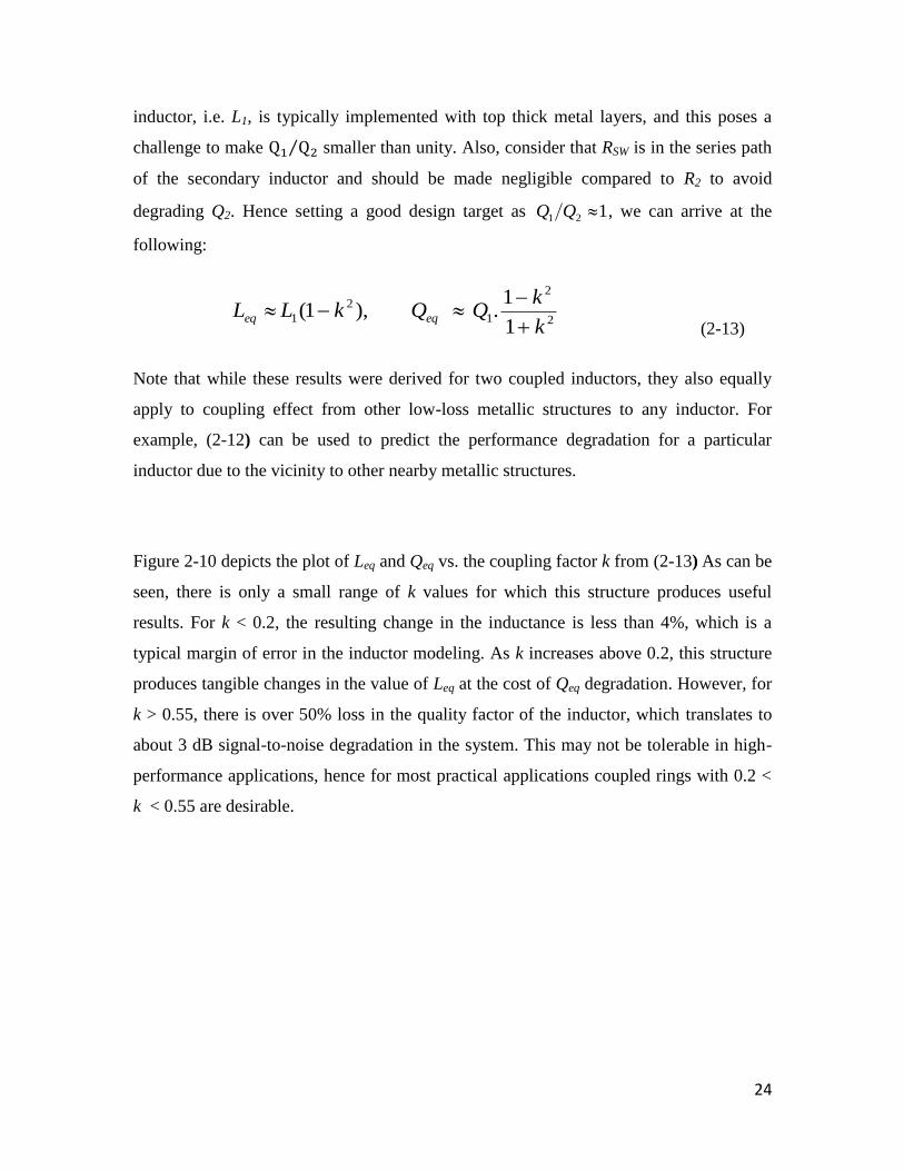
For simplicity, consider that the two inductors are formed by two co-centric loops of
current as shown in the Figure 2-11. With this assumption, we can use the equation for
the self-inductance of a current loop, derived in [32] :
11 RL , 22 RL
( 2-14)
The mutual inductance, from the electromagnetic theory, is computed as
where
is the magnetic flux through the loop P2 due to I1 current and dS is
the surface element in loop P1.
26
R1
R2
A2 Area
I1
P2 Perimeter
A1 Area
P1 Perimeter
O
Figure 2-11 Two coupled rings as two co-centric loops of currents I1 and I2
The magnetic field of I1 at the center of the loop, i.e. point ‘O’ in Figure 2-11, is:
1
11
2R
IB
( 2-15)
If R2 << R1, one can approximate the field inside P2 with that of expression (2-15) hence
1
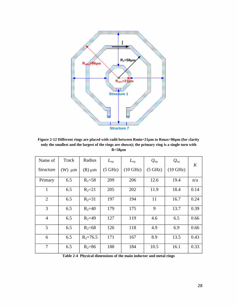
2
2
1
2
2
1
1
1
1
2
1..
2
.
2
R
R
IR
R
I
I
dSB
MA
( 2-16)
which in combination with (2-14) results in:
1
2
1
2
2 R
R
R
Rk
( 2-17)
This formula is only valid for small values of R2. Nonetheless, it reveals an important
property of co-centric coupled rings, i.e. the coupling factor is only a function of R2/R1,
the radius ratio of the two rings that in turn is an indication of their relative proximity.
Unfortunately (2-17) falls short of predicting k with sufficient accuracy for practical
values of R2/R1. The proper calculation requires more elaborate analysis; details are

27
presented in Appendix A. Interestingly, the final result still indicates that the coupling k is
only a function of the ratio of the radii of the two loops (i.e., k = f(R2/R1):
21
212 2
,)]()().2
1[(2
RR
RREKk
( 2-18)
where K(γ) and E(γ) are complete elliptic functions of first and second order,
respectively. The Tables of K and E function for different values of γ are widely available
[40].
A simple expression that is valid for most practical values of k, hereinafter called region
of practical k tuning (0.2< k <0.55), is given by (derivation also presented in Appendix
A):
))(11( 2
1
2
2
1
R
R
R
Rk
( 2-19)
Interestingly, for small values of 12 RR where the relation
2
12
2
12 )(5.011 RRRR holds, (2-19) translates to that of (2-17); a result that is
not unexpected.
2.5 Simulation Results
In order to confirm the analysis presented in the previous section, a 3D simulator
(integrand) is used to simulate Leq and Qeq for different values of R2 and R1.
The primary inductor in this simulation is a single-turn inductor with the average radius
of 58 µm implemented in the top two thick metal layers, i.e. doubly-stacked M9 and M8.
The simulated values of the inductance and the quality factor are 209 pH and 12.6,
respectively, at 5 GHz (first row of Table 2-4).
28
R1=58µm
Rmin=21µm
Rmax=86µm
I
Structure 1
Structure 7
Figure 2-12 Different rings are placed with radii between Rmin=21µm to Rmax=86µm (for clarity
only the smallest and the largest of the rings are shown); the primary ring is a single turn with
R=58µm
Name of
Structure
Track
(W) m
Radius
(R) m
Leq
(5 GHz)
Leq
(10 GHz)
Qeq
(5 GHz)
Qeq
(10 GHz) K
Primary 6.5 R1=58 209 206 12.6 19.4 n/a
1 6.5 R2=21 205 202 11.9 18.4 0.14
2 6.5 R2=31 197 194 11 16.7 0.24
3 6.5 R2=40 179 175 9 13.7 0.39
4 6.5 R2=49 127 119 4.6 6.5 0.66
5 6.5 R2=68 126 118 4.9 6.9 0.66
6 6.5 R2=76.5 171 167 8.9 13.5 0.43
7 6.5 R2=86 188 184 10.5 16.1 0.33
Table 2-4 Physical dimensions of the main inductor and metal rings

29
Figure 2-13 The variation of Leq vs. the radius of the coupled secondary ring; regions of practical k
tuning are highlighted
In order to change the inductance, a family of metal rings are placed inside and outside
this inductor as shown in Figure 2-12. The radii of these rings are varied from
R2,min=21µm to R2,max=86µm. Following the recommendations of the previous discussion,
Q2 is increased by implementing the metal rings in the top two metal layers which
improves Qeq. The equivalent inductance, quality factor and the coupling factor are
simulated for each case and are also presented in Table 2-4.
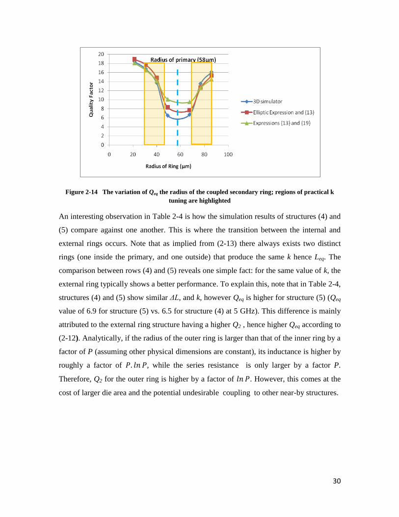
Figure 2-13 and Figure 2-14 show the plots of simulated Leq and Qeq, respectively. To
compare the simulation results with those of presented analysis the values obtained from
the analytical expressions of k, i.e., the elliptic equation of (2-18) and the simplified
equation of (2-19), are employed in ( 2-13). As can be seen in both graphs, Elliptic
expression closely predicts the coupling factor, the equivalent inductance and quality
factor of the coupled rings.
Even the simplified expression of (2-19) when used in the region of practical k tuning
predicts Leq and Qeq with an error less than 10%. These results show that designers can
safely use these simple expressions to design and floorplan their coupled rings even
before they start using 3D simulators to fine-tune the design.
30
Figure 2-14 The variation of Qeq the radius of the coupled secondary ring; regions of practical k
tuning are highlighted
An interesting observation in Table 2-4 is how the simulation results of structures (4) and
(5) compare against one another. This is where the transition between the internal and
external rings occurs. Note that as implied from ( 2-13) there always exists two distinct
rings (one inside the primary, and one outside) that produce the same k hence Leq. The
comparison between rows (4) and (5) reveals one simple fact: for the same value of k, the
external ring typically shows a better performance. To explain this, note that in Table 2-4,
structures (4) and (5) show similar ΔL, and k, however Qeq is higher for structure (5) (Qeq
value of 6.9 for structure (5) vs. 6.5 for structure (4) at 5 GHz). This difference is mainly
attributed to the external ring structure having a higher Q2 , hence higher Qeq according to
(2-12). Analytically, if the radius of the outer ring is larger than that of the inner ring by a
factor of P (assuming other physical dimensions are constant), its inductance is higher by
roughly a factor of , while the series resistance is only larger by a factor P.
Therefore, Q2 for the outer ring is higher by a factor of . However, this comes at the
cost of larger die area and the potential undesirable coupling to other near-by structures.
31
2.6 Measurement Results
To validate the analytical and simulation results of the previous sections, a few coupled-
ring structures are simulated and laid out in a CMOS Process. The primary inductor is a
two-turn doubly-stacked spiral (M8 and M9 are joined together by a large number of vias)
with pattern ground shield underneath and a solid ground ring around the whole structure
on all metal layers for best noise isolation. The simulation results of the primary inductor
show an inductance of 405 pH and a quality factor of 11.8 at 5 GHz. In order to change
the inductance value, two rings are placed inside and outside the primary. The outer ring
is comparably narrower (lower Q), and is placed closer to the primary (5 µm away),
while the inner ring is wider (higher Q), and placed farther inside the primary loop (15
µm away). Four variants of such structure were placed on die, as listed below and shown
in Figure 2-15:
Figure 2-15 The test inductors implemented in a CMOS process: (A) primary inductor with both
rings open, (B) Inner loop shorted, outer loop open, (C) Inner loop open, outer loop shorted, (D) Both
loops shorted
32
A) Both loops open
B) Inner loop shorted, outer loop open
C) Inner loop open, outer loop shorted
D) Both loops shorted
Leq (pH) Qeq Radius (µm) Measured
k
Estimated k
(Eq. 19)
A 405 11.8 48 µm primary only N/A N/A
B 388 10.8 18µm
inner ring shorted 0.2 0.19
C 329 6.1 67µm
outer ring shorted 0.43 0.41
D 318 4.9 Both rings shorted N/A N/A
Table 2-5 De-embedded measurement results for the four structures of Figure 2-14
The measured values of Leq, Qeq, and k are shown in Table 2-5 for all the four
combinations mentioned above. It is interesting to observe that predictions of (2-18)
using R1 and R2 for each ring are very close to those of the measurements. Note that the
derivation of (2-18) in Appendix assumes a single loop of current for the primary
inductor, while the implemented primary inductor is a two-turn spiral. Deriving the exact
value of R1 for such a structure, i.e. the equivalent loop radius, entails more complicated
calculations. However, as a first-order estimate R1 is approximated as (Din+Dout)/4 ~
48µm, where Din and Dout represent the inner and outer diameters of the two-turn spiral,
respectively.
Note the large drop in the value of Qeq for structures C and D. This is due to the outer
ring being of a lower quality factor (outer ring Q2 is 5.5 at 5 GHz) compared to the
primary ring (11.8 at 5 GHz). The value of Qeq as predicted by (2-12) i.e. general
33
expression, is 6.7 compared to the measured value of 6.1. On the other hand, for structure
B, the inner ring has a high quality factor (Q2 = 10.5 at 5 GHz), which causes less
degradation on Qeq. This allows the use of (2-13) for Qeq, i.e. good design target
expression, which predicts Qeq of 10.9 for that structure (in close agreement with the
measured value of 10.8).
2.7 Conclusion
On-chip spiral inductors are becoming increasingly popular in DSM analog and RF
design. The accuracy of modeling tools and the designer’s intuition are both necessary
elements for a successful design. This chapter attempts to tackle the two issues by design,
analysis and measurement comparison of different inductor structures. To facilitate the
usage of a few unconventional inductors such as helical and coupled-ring structures,
analytical expressions are derived and presented. The proposed study allows for fast and
reliable design and optimization of these structures in CMOS technology. Measurement
results of the prototype test structures validate the usefulness of the proposed analysis.

34
Chapter 3
Analysis, Design, Optimization and
Fabrication of Push-Push LC-VCO in
CMOS
The design of high frequency oscillators entails a challenging trade-off among several
parameters including the phase noise, frequency tuning range, power consumption and
silicon area. The integration of high-performance mm-wave voltage-controlled oscillators
(VCOs) into the low-cost digital CMOS technologies is a subject of wide research
interest [41-44]. The relatively low ft frequency of CMOS process as compared to other
technologies such as BiCMOS and HBTs, the higher flicker noise and the limitations of
interconnect and device parasitics are among major bottlenecks of high frequency CMOS
VCO design. Several architectures have been proposed to address the aforementioned
challenges [42-44].
We start this chapter by an overview of popular oscillator architectures and recent
designs in the realm of mm-wave LC-VCOs. Push-push VCOs are shown to be an
attractive solution for high frequency designs. To study the nature of 2nd
harmonic
generation in LC-VCOs, an analytical framework is developed in section 3.4. The output
voltage of an LC-VCO with an accumulation-mode MOS (AMOS) varactor is analyzed
from a large-signal perspective and the amplitude of the 2nd
harmonic is expressed in
terms of the circuit parameters. It is shown that the magnitude of this harmonic is a strong
function of the shape of the varactor C-V characteristics. The analysis is supported by
simulations to confirm this dependence. The result of this analysis is verified by design,
fabrication and measurement of two wide tuning-range low-phase-noise push-push VCOs
employing thin-oxide and thick-oxide AMOS devices, respectively.
35
3.1 VCO Architectures
3.1.1 Ring Oscillators
The simplest form of an oscillator is composed of several gain stages in a feedback loop
as shown in Figure 3-1 The principle conditions for oscillation of a negative-feedback
amplifier known as “Barkhausen criteria” are as follows [45][46]
Even number of inversions
Figure 3-1 Schematic of a ring oscillator
180)(
1)(
0
0
jH
jH
( 3-1)
where H(jω) is the loop gain transfer function. Ring oscillators are very popular clock
generators in the digital and mixed-signal applications mainly because of their wide
tuning range and compact implementation. However, they suffer from a relatively large
phase noise which prohibits their use in application with tough jitter specifications [47].
Particularly, in wireless applications where many neighboring channels reside a few kHz
from each other, it is usually not possible to meet the stringent inter-modulation
requirements using ring oscillators.
36
3.1.2 LC Oscillators
The inherently better phase noise of LC oscillators in comparison to their ring oscillators
counterparts made them very popular in wireless applications [48]. In addition, the fine-
tuning capability of this class of oscillators (using on-chip varactors, and variable
inductors) without the need for extra voltage-to-current (voltage-to-voltage) converter
blocks enables their efficient integration into a PLL[49].
Returning to the generic LC-VCO shown in Figure 1-2 (inset), we re-draw the circuit
(Figure 3-2) and start analyzing this circuit by first ignoring the LC tank.
Lp
Cp
Figure 3-2 Schematic of a generic LC-VCO
The structure of two back-to-back inverters normally constitutes a latch, which is capable
of holding an initial value simply like a memory cell.

37
From another perspective, there are only two (even) number of inverter stages in the loop
and, one does not expect this loop to oscillate (unlike ring oscillators it does not satisfy
the phase requirement of (3-1). However, the addition of an LC tank across the structure
nullifies its memory property (note that inductor acts as a short in DC and does not allow
the '1' and '0', i.e. a net DC voltage across inductor, to latch in the cell) and causes the
loop to oscillate due to the resonance effect. Now, the inverters only act as energy-
providers to compensate for the losses in the LC tank. This allows simplifying the active
part of the circuit (as long as it provides the minimum required energy to sustain the
oscillation) to reduce the output noise. One example of this simplification is the Colpitts
oscillator shown in Figure 3-3.
Figure 3-3 Colpitts Oscillator
In this classical Colpitts VCO with capacitive feedback from drain to source, it can be
shown that the circuit oscillates if gmRp ≥ 4 [46], where gm is the transconductance of
MOS transistor and Rp is the equivalent parallel resistance seen at the drain of the
transistor, and includes non-idealities of inductors and capacitors. The frequency of
oscillation is given by:
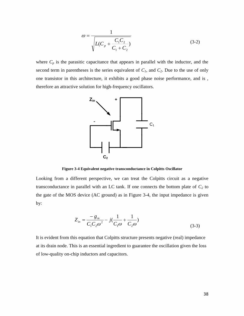
38
)(
1
21
21
CC
CCCL p
( 3-2)
where Cp is the parasitic capacitance that appears in parallel with the inductor, and the
second term in parentheses is the series equivalent of C1, and C2. Due to the use of only
one transistor in this architecture, it exhibits a good phase noise performance, and is ,
therefore an attractive solution for high-frequency oscillators.
+
-
C2
C1
Zin
Figure 3-4 Equivalent negative transconductance in Colpitts Oscillator
Looking from a different perspective, we can treat the Colpitts circuit as a negative
transconductance in parallel with an LC tank. If one connects the bottom plate of C2 to
the gate of the MOS device (AC ground) as in Figure 3-4, the input impedance is given
by:
)11
(21
2
21 CC
jCC
gZ m
in
( 3-3)
It is evident from this equation that Colpitts structure presents negative (real) impedance
at its drain node. This is an essential ingredient to guarantee the oscillation given the loss
of low-quality on-chip inductors and capacitors.
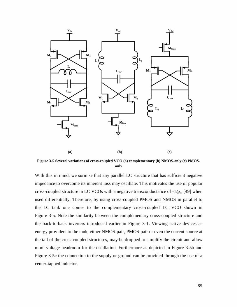
39
M1
Cvar
Vdd
L
M3 M4
Mbias
M2
M1
Cvar
Vdd
L1
Mbias
M2
L2
Cvar
Vdd
L1
M1 M2
L2
Mbias
(a) (b) (c)
Figure 3-5 Several variations of cross-coupled VCO (a) complementary (b) NMOS-only (c) PMOS-
only
With this in mind, we surmise that any parallel LC structure that has sufficient negative
impedance to overcome its inherent loss may oscillate. This motivates the use of popular
cross-coupled structure in LC VCOs with a negative transconductance of -1/gm [49] when
used differentially. Therefore, by using cross-coupled PMOS and NMOS in parallel to
the LC tank one comes to the complementary cross-coupled LC VCO shown in
Figure 3-5. Note the similarity between the complementary cross-coupled structure and
the back-to-back inverters introduced earlier in Figure 3-1. Viewing active devices as
energy providers to the tank, either NMOS-pair, PMOS-pair or even the current source at
the tail of the cross-coupled structures, may be dropped to simplify the circuit and allow
more voltage headroom for the oscillation. Furthermore as depicted in Figure 3-5b and
Figure 3-5c the connection to the supply or ground can be provided through the use of a
center-tapped inductor.

40
3.2 LC-VCO Phase Noise
The noise on the output phase of VCO, as the clock generator for most wireline and
wireless transceivers, may severely degrade the signal to noise ratio (SNR) in both the
receive and transmit paths. The output of a VCO may be written as V(t)=Acos(ω0t+φn(t))
where A, and ω0 are the amplitude, and fundamental frequency, respectively. The term
φn(t) represents the random variations in the phase of oscillator in the time domain, and
may be viewed as skirts to the ideal response of an oscillator in the frequency domain
[48] (Figure 3-6a) The spectrum of phase-noise can be decomposed into three distinct
regions, as shown in Figure 3-6b:
1) Rapid roll-off around the carrier (called close-in phase noise) with 1/Δf 3 roll-off rate
where Δf is the offset from the carrier
2) 1/Δf 2 in the intermediate offsets (some-times called out-of-band region).
3) Flat region where the phase noise is dominated by the noise floor of the output path.
There are several methods of analyzing phase noise in oscillators. The linear time-
invariant (LTI) model relies on finding the noise voltage across the tank by calculating
the current noise, and then multiplying it by the impedance of tank around the resonance
frequency. Using this analysis in combination with practical curve fit-fitting techniques,
the Leeson formula is arrived at [50]:
)]1()2
(12
[3/120
f
sig QP
FKTL
( 3-4)
In a more elaborate analysis, using linear time-variant (LTV) model of the phase noise,
Hajimiri and Lee [51] introduced a cyclo-stationary function called Impulse Sensitivity
Function (ISF), Γ(t), that explains many shortcoming of the LTI model. The use of this
function captures the different behaviors of the oscillator when excited by noise sources
in different instants of time. For example an input noise source applied at zero-crossing

41
(a) (b)
Figure 3-6 a)Time, and frequency domain representation of phase noise, b) Different regions of LC
VCO phase noise
instant of an oscillator waveform can generate far greater phase noise than one applied at
any maxima or minima. Using this LTV model phase noise of an oscillator can be
rewritten as [51] :,
2max
2
0
22
4log.10)(
q
cf
i
L m
mn
SBC
( 3-5)
where in2 represents all noise sources (currents here) in the VCO, cm are Fourier
coefficients of ISF function, qmax = cVmax is the maximum charge across the tank, and Δω
is the offset frequency. The importance of this expression is that it quantifies the phase
noise in terms of the circuit parameters. For instance, it can be shown that the close-in
phase-noise (1/f 3
region in Figure 3-6b) is closely related to the symmetry properties of
cross-coupled pair. Therefore, matching the rise and fall times of VCO waveform can
reduce the close-in phase noise. It can be shown that proper matching of rise and fall
times significantly reduces the first Fourier coefficient (c0) of ISF function, hence the
phase noise.
42
3.3 High-Frequency and mm-Wave LC-VCO Design
Since the proliferation of multi-gigahertz operation, several studies have been conducted
toward the realization of high-performance oscillators. There has been much focus on
LC-type VCOs specifically Colpitts, and cross-coupled architectures mainly due to their
superior noise performance.
In [52] a 16 GHz differential Colpitts VCO is realized in 0.18µm BiCMOS technology.
The choice of Colpitts in this design is mainly based on the fact that it generally
possesses a smaller RMS, and DC values of ISF compared to the cross-coupled
counterpart [53]. A schematic of this VCO is shown in Figure 3-7a. A PMOS-type
Colpitts design is adopted in this work due to lower flicker noise of PMOS devices. The
DC current source, in traditional Colpitts design, is replaced by an RF choke to avoid any
headroom degradation caused by the use of active devices. A center-tapped inductor
(connected to Vdd) provides the DC current for the core of the VCO. In order to drive the
50 Ω impedance of the measurement device a source-follower buffer is inserted at the
output of VCO. This buffer architecture is preferred over the typical open-drain one to
avoid the addition of a matching circuitry required at 16 GHz, though the latter provides a
higher gain. This oscillator resonates at 16.5 GHz with a phase-noise of -115 dBc/Hz at
an offset of 1 MHz. The entire circuit consumes 43 mW of power (30 mW core VCO,
and 13 mW buffer).
In another work [54], an NMOS cross-coupled VCO with a PMOS current source is
employed to achieve oscillation at 60 GHz. The use of PMOS at the center-tap of the
inductor allows the bias of Vdrain (as depicted in Figure 3-7b) at around the mid-rail, i.e.
Vdd/2. This allows full deployment of the varactor tuning range by sweeping the control
voltage, Vtune, from 0 to Vdd. One particular aspect of the high-frequency VCO considered
by this work is the critical impact of varactor Q in supra-10 GHz applications. As
discussed in the previous chapter, in the mm-wave frequency range the Q of the tank is
constrained by the varactor’s QC, see (2-7). In this work it is shown that the quality factor
of varactor is given by:
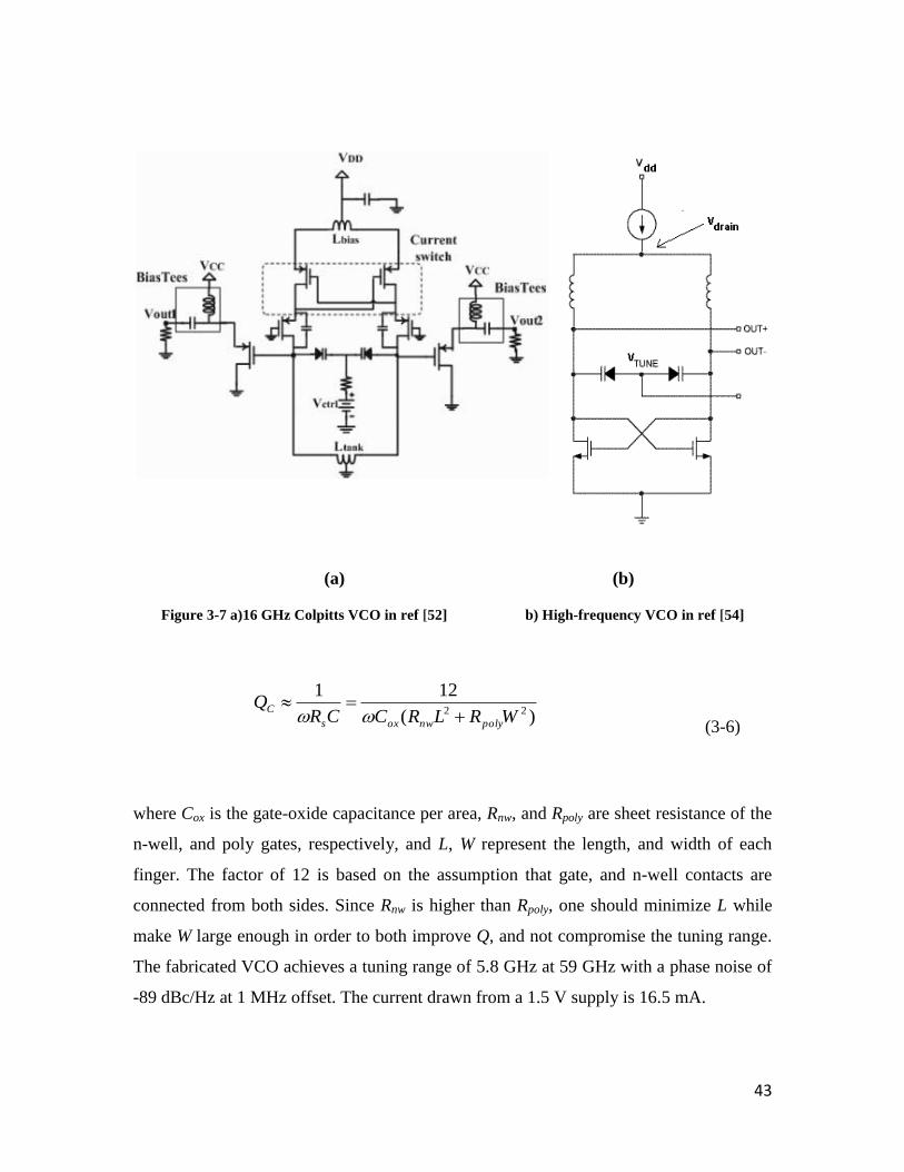
43
(a) (b)
Figure 3-7 a)16 GHz Colpitts VCO in ref [52] b) High-frequency VCO in ref [54]
)(
12122 WRLRCCR
Qpolynwoxs
C
( 3-6)
where Cox is the gate-oxide capacitance per area, Rnw, and Rpoly are sheet resistance of the
n-well, and poly gates, respectively, and L, W represent the length, and width of each
finger. The factor of 12 is based on the assumption that gate, and n-well contacts are
connected from both sides. Since Rnw is higher than Rpoly, one should minimize L while
make W large enough in order to both improve Q, and not compromise the tuning range.
The fabricated VCO achieves a tuning range of 5.8 GHz at 59 GHz with a phase noise of
-89 dBc/Hz at 1 MHz offset. The current drawn from a 1.5 V supply is 16.5 mA.
44
In yet another recent work in [55], the VCO tuning is implemented using the intrinsic
capacitance of the core transistors to avoid the use of lossy varactors. The idea behind
this work is to employ the voltage-dependent junction capacitors of a MOS device in
place of tank varactors. A triple-well NMOS device has several junction capacitances
suitable for this purpose. In particular, one is able to change the drain-bulk capacitance by
applying a voltage to the bulk node of this configuration. By varying the bulk voltage
between 0 and 1V, the depletion capacitance of this region changes from 8.9 fF to 12.1 fF
for the NMOS device used in this design (Vbulk values exceeding 1V may forward bias the
junction and should be avoided). This results in an overall cap change of 10% for the
NMOS structure. Using a low-loss spiral inductor (QL 20), this VCO achieves an
oscillation frequency of 69.8 GHz. Measured tuning range of 4.5% (66.7 GHz to
69.8 GHz) is reported for this VCO.
A different approach to alleviate the problem of varactor loss at high frequencies is to
tune the circuit for a lower frequency (lower varactor loss) and multiply up its output to
generate the desired frequency. In [56] a source degeneration technique (as shown in
Figure 3-8a) is proposed that allows the extraction of the 2nd
harmonic content of the
fundamental oscillation. It is analytically shown that the squaring function of M1-M2 pair
provides a frequency doubling effect. This effect, in turn, generates two in-phase 2nd
harmonic signals at the source node of the differential pair which is then extracted at the
common-mode connection of the two degeneration capacitors, CS, and is amplified
through the use of a single-ended tuned amplifier. Therefore, to generate 60 GHz output
signal, the LC tank circuit is required to operate only up to 30 GHz resulting in an
improved quality factor. The VCO consumes 30 mW (including the VCO core and the
following amplifier at 2fo) from a 1.2 V supply and the measured phase noise at 1 MHz
offset is -89 dBc/Hz.
The concept of extracting and amplifying the 2nd
harmonic offers oscillation frequencies
above the fundamental frequency of a conventional oscillator. This family of oscillators
called push-push are attractive solutions for the wide-tuning-range and high frequency
VCO applications.

45
In [57] another extraction technique for push-push VCO is proposed, where the
differential 2nd
harmonic signal is generated at two source nodes of NMOS and PMOS
pairs. When VCO operates in the voltage-limited regime, a second harmonic current (due
to the push-push effect) flows through the impedance from each source node to supply
(ground) as shown in Figure 3-8b. The usefulness of the proposed architecture is
experimentally verified by the implementation of a CMOS VCO in 0.13-µm CMOS
process and an output frequency range of 5.47-5.77 GHz.
(a) (b)
Figure 3-8 a) Push Push VCO presented in [56] b) 2nd
harmonic extraction technique in [57]
3.4 Second Harmonic Generation in AMOS-Based LC tank
As discussed, in the push-push VCO design the concept of harmonic
amplification is used to constructively add the even-order harmonics of the VCO’s
fundamental frequency. Works presented in the literature focus on extracting the signal
from a common-mode node of the differential oscillator where the 2nd
harmonic is

46
generated by two time-interleaved voltage (current) switching caused by the two halves
of the circuit, i.e. the common source of a cross-coupled pair or the power supply
connection [56-58].
In this section, we analyze the LC tank in an AMOS-based LC VCO. A closer study of
the non-linear differential equations governing the behavior of this tank reveals that the
2nd
harmonic signal may alternatively be generated by the periodic change of the tank
capacitance.
3.4.1 Small-Signal Analysis
Figure 3-9 illustrates the equivalent model for a cross-coupled LC-VCO with an AMOS
varactor. The negative transconductance, -gactive, is the equivalent transconductance of the
cross-coupled active devices. In the steady state, the tank parallel loss, Rtank, and the
negative active resistance, -1/gactive, cancel each other. The remaining circuit is a lossless
LC tank with a variable capacitor (varactor) that oscillates given a non-zero initial
condition. The charge stored on the capacitor C at any instance of time is given by dQ =
C(V).dV.
v(t)
+
-
Figure 3-9 LC Tank Circuit
Thus, we have a differential equation, which defines the oscillation voltage V(t):
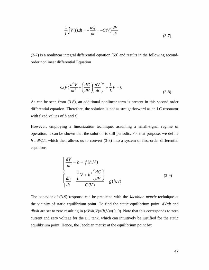
47
dt
dVVC
dt
dQdttV
L)().(
1
( 3-7)
(3-7) is a nonlinear integral differential equation [59] and results in the following second-
order nonlinear differential Equation
01
)(
2
2
2
V
Ldt
dV
dV
dC
dt
VdVC
( 3-8)
As can be seen from (3-8), an additional nonlinear term is present in this second order
differential equation. Therefore, the solution is not as straightforward as an LC resonator
with fixed values of L and C.
However, employing a linearization technique, assuming a small-signal regime of
operation, it can be shown that the solution is still periodic. For that purpose, we define
h = dV/dt, which then allows us to convert (3-8) into a system of first-order differential
equations
),()(
1
),(
2
vhgVC
dV
dChV
L
dt
dh
Vhfhdt
dV
( 3-9)
The behavior of (3-9) response can be predicted with the Jacobian matrix technique at
the vicinity of static equilibrium point. To find the static equilibrium point, dV/dt and
dh/dt are set to zero resulting in (dV/dt,V)=(h,V)=(0, 0). Note that this corresponds to zero
current and zero voltage for the LC tank, which can intuitively be justified for the static
equilibrium point. Hence, the Jacobian matrix at the equilibrium point by:
48
0)0(
110
)0,0()0,0(
)0,0()0,0(
LCh
g
V
gh
f
V
f
( 3-10)
where C(0) = CDC in (3-10) refers to the DC (bias) capacitance of varactor in the absence
of any oscillation, i.e. V(t)=0. The eigenvalues of this matrix, which are the poles of the
linearized system, determine the behavior of the system around the static equilibrium
point, i.e., whether the response is oscillatory, over damped, or underdamped. Since the
eigenvalues of this matrix are purely imaginary ( DCLCj ), V(t) oscillates around the
equilibrium point with the angular frequency of DCLC10 .
This solution is, of course, valid as long as V(t) stays in the small-signal regime of
operation. However, in most practical LC-VCO designs V(t) does not satisfy this
condition and the angular frequency (ω) starts to deviate from the value given by ω0. To
derive the analytical expression for the angular frequency we need to re-visit (3-7)
accounting for the large signal variations.
3.4.2 Large-Signal Analysis
Figure 3-10a shows the cross section of an accumulation-mode varactor. n+ regions are
buried in an n-well which in turn guarantees the device does not enter inversion and
creates a monotonic C-V characteristics [60].
To analyze large-signal oscillation, one requires to model the voltage-dependant nature of
C(V) in order to solve (3-7). The C-V characteristics of a typical AMOS varactor (as
shown in Figure 3-10b) is modeled as [61]:

49
2V1
V0
C0
C0+C1
C0-C1
C
VGSVmin Vmax
(a) (b)
Figure 3-10 C-V a) Cross section of an accumulation-mode MOS varactor (AMOS) b) The
characteristics of AMOS varactor
)V
-VV.Tanh(+C)=CC(V GS
GS
1
0
10
( 3-11)
where C0, C1, V0 and V1 are shown in the Figure 3-10b and VGS represents the
instantaneous gate-source voltage across the varactor. Note that during the oscillation, the
gate plate of varactor is continuously modulated by the output voltage while its source
node is held at a fixed voltage (called Vctrl) corresponding to the desired frequency.
Therefore, one can write VGS V(t) from an AC perspective.
In the steep region, (3-11) can be linearized as:
C(V) )V
V-V.(+CC
1
0
10 = CDC +KV
( 3-12)
where CDC is a fixed term that includes all the parasitic capacitances in the tank, and K =
C1/V1 represents the slope of C-V characteristics in the steep region. Using this
approximation, (3-7) simplifies to:
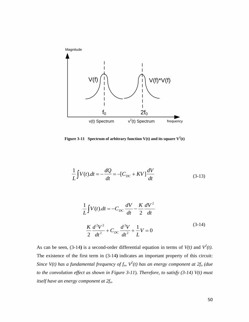
50
Magnitude
f0
V(f) V(f)*V(f)
2f0
frequencyv(t) Spectrum v2(t) Spectrum
Figure 3-11 Spectrum of arbitrary function V(t) and its square V2(t)
dt
dVKVC
dt
dQdttV
LDC ][).(
1
( 3-13)
dt
dVK
dt
dVCdttV
LDC
2
2).(
1
01
2 2
2
2
22
VLdt
VdC
dt
VdKDC
( 3-14)
As can be seen, (3-14) is a second-order differential equation in terms of V(t) and V2(t).
The existence of the first term in (3-14) indicates an important property of this circuit:
Since V(t) has a fundamental frequency of fo, V2(t) has an energy component at 2fo (due
to the convolution effect as shown in Figure 3-11). Therefore, to satisfy ( 3-14) V(t) must
itself have an energy component at 2fo.
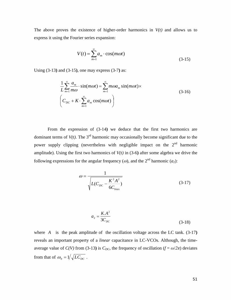
51
The above proves the existence of higher-order harmonics in V(t) and allows us to
express it using the Fourier series expansion:
1
)cos()(m
m tmatV
( 3-15)
Using (3-13) and (3-15), one may express (3-7) as:
1
11
)cos(
)sin()sin(1
m
mDC
m
m
m
m
tmaKC
tmamtmm
a
L
( 3-16)
From the expression of (3-14) we deduce that the first two harmonics are
dominant terms of V(t). The 3rd
harmonic may occasionally become significant due to the
power supply clipping (nevertheless with negligible impact on the 2nd
harmonic
amplitude). Using the first two harmonics of V(t) in ( 3-6) after some algebra we drive the
following expressions for the angular frequency (), and the 2nd
harmonic (a2):
)6
(
1
22
bias
DCC
AKCL
( 3-17)
DCC
AKa
3
. 2
2
( 3-18)
where A is the peak amplitude of the oscillation voltage across the LC tank. (3-17)
reveals an important property of a linear capacitance in LC-VCOs. Although, the time-
average value of C(V) from (3-13) is CDC, the frequency of oscillation (f = ω/2π) deviates
from that of DCLC10 .
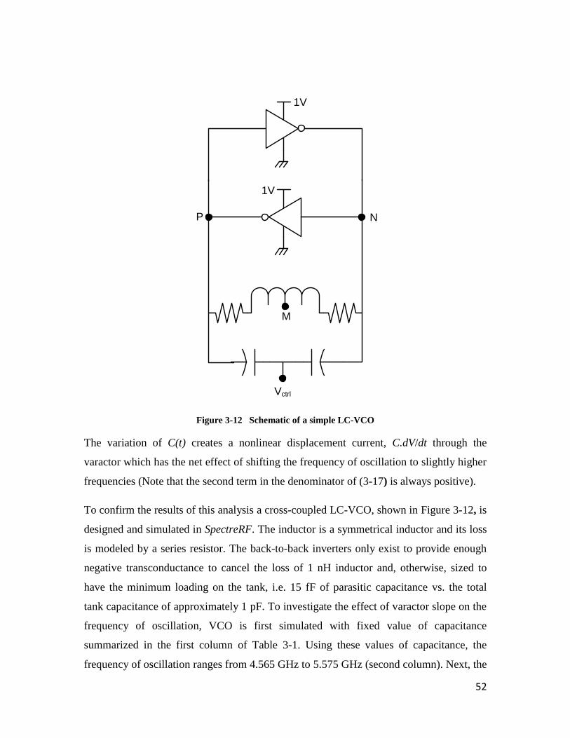
52
Vctrl
P N
M
1V
1V
Figure 3-12 Schematic of a simple LC-VCO
The variation of C(t) creates a nonlinear displacement current, C.dV/dt through the
varactor which has the net effect of shifting the frequency of oscillation to slightly higher
frequencies (Note that the second term in the denominator of ( 3-17) is always positive).
To confirm the results of this analysis a cross-coupled LC-VCO, shown in Figure 3-12, is
designed and simulated in SpectreRF. The inductor is a symmetrical inductor and its loss
is modeled by a series resistor. The back-to-back inverters only exist to provide enough
negative transconductance to cancel the loss of 1 nH inductor and, otherwise, sized to
have the minimum loading on the tank, i.e. 15 fF of parasitic capacitance vs. the total
tank capacitance of approximately 1 pF. To investigate the effect of varactor slope on the
frequency of oscillation, VCO is first simulated with fixed value of capacitance
summarized in the first column of Table 3-1. Using these values of capacitance, the
frequency of oscillation ranges from 4.565 GHz to 5.575 GHz (second column). Next, the
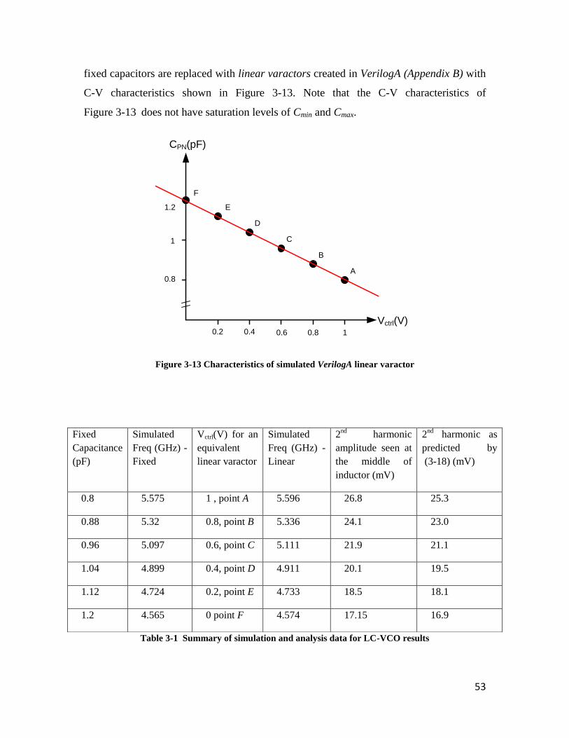
53
fixed capacitors are replaced with linear varactors created in VerilogA (Appendix B) with
C-V characteristics shown in Figure 3-13. Note that the C-V characteristics of
Figure 3-13 does not have saturation levels of Cmin and Cmax.
CPN(pF)
Vctrl(V)
0.8
1
1.2
10.6 0.80.40.2
A
B
C
D
E
F
Figure 3-13 Characteristics of simulated VerilogA linear varactor
Table 3-1 Summary of simulation and analysis data for LC-VCO results
Fixed
Capacitance
(pF)
Simulated
Freq (GHz) -
Fixed
Vctrl(V) for an
equivalent
linear varactor
Simulated
Freq (GHz) -
Linear
2nd
harmonic
amplitude seen at
the middle of
inductor (mV)
2nd
harmonic as
predicted by
(3-18) (mV)
0.8 5.575 1 , point A 5.596 26.8 25.3
0.88 5.32 0.8, point B 5.336 24.1 23.0
0.96 5.097 0.6, point C 5.111 21.9 21.1
1.04 4.899 0.4, point D 4.911 20.1 19.5
1.12 4.724 0.2, point E 4.733 18.5 18.1
1.2 4.565 0 point F 4.574 17.15 16.9
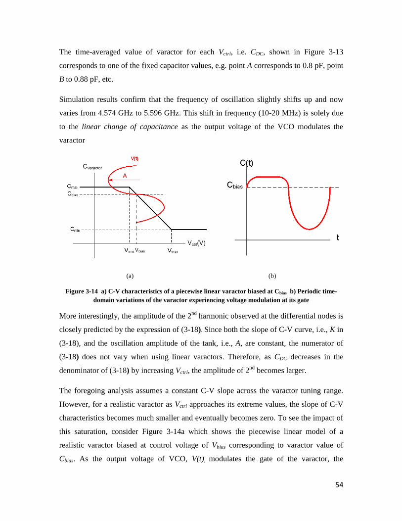
54
The time-averaged value of varactor for each Vctrl, i.e. CDC, shown in Figure 3-13
corresponds to one of the fixed capacitor values, e.g. point A corresponds to 0.8 pF, point
B to 0.88 pF, etc.
Simulation results confirm that the frequency of oscillation slightly shifts up and now
varies from 4.574 GHz to 5.596 GHz. This shift in frequency (10-20 MHz) is solely due
to the linear change of capacitance as the output voltage of the VCO modulates the
varactor
(a) (b)
Figure 3-14 a) C-V characteristics of a piecewise linear varactor biased at Cbias b) Periodic time-
domain variations of the varactor experiencing voltage modulation at its gate
More interestingly, the amplitude of the 2nd
harmonic observed at the differential nodes is
closely predicted by the expression of (3-18). Since both the slope of C-V curve, i.e., K in
(3-18), and the oscillation amplitude of the tank, i.e., A, are constant, the numerator of
(3-18) does not vary when using linear varactors. Therefore, as CDC decreases in the
denominator of ( 3-18) by increasing Vctrl, the amplitude of 2nd
becomes larger.
The foregoing analysis assumes a constant C-V slope across the varactor tuning range.
However, for a realistic varactor as Vctrl approaches its extreme values, the slope of C-V
characteristics becomes much smaller and eventually becomes zero. To see the impact of
this saturation, consider Figure 3-14a which shows the piecewise linear model of a
realistic varactor biased at control voltage of Vbias corresponding to varactor value of
Cbias. As the output voltage of VCO, V(t), modulates the gate of the varactor, the
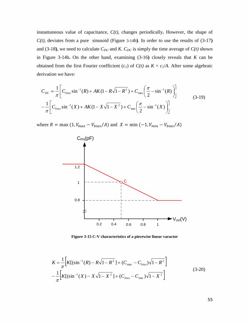
55
instantaneous value of capacitance, C(t), changes periodically. However, the shape of
C(t), deviates from a pure sinusoid (Figure 3-14b). In order to use the results of (3-17)
and (3-18), we need to calculate CDC and K. CDC is simply the time average of C(t) shown
in Figure 3-14b. On the other hand, examining (3-16) closely reveals that K can be
obtained from the first Fourier coefficient (c1) of C(t) as K = c1/A. After some algebraic
derivation we have:
)(sin2
)11()(sin1
)(sin2
)11()(sin1
1
min
21
1
max
21
XCXXAKXC
RCRRAKRCC
bias
biasDC
( 3-19)
where and
Figure 3-15 C-V characteristics of a piecewise linear varactor
2
min
21
2
max
21
1)(]1)([(sin1
1)(]1)([(sin1
XCCXXXK
RCCRRRKK
bias
bias
( 3-20)
CPN(pF)
Vctrl(V)
0.8
1
1.2
10.6 0.80.40.2
C
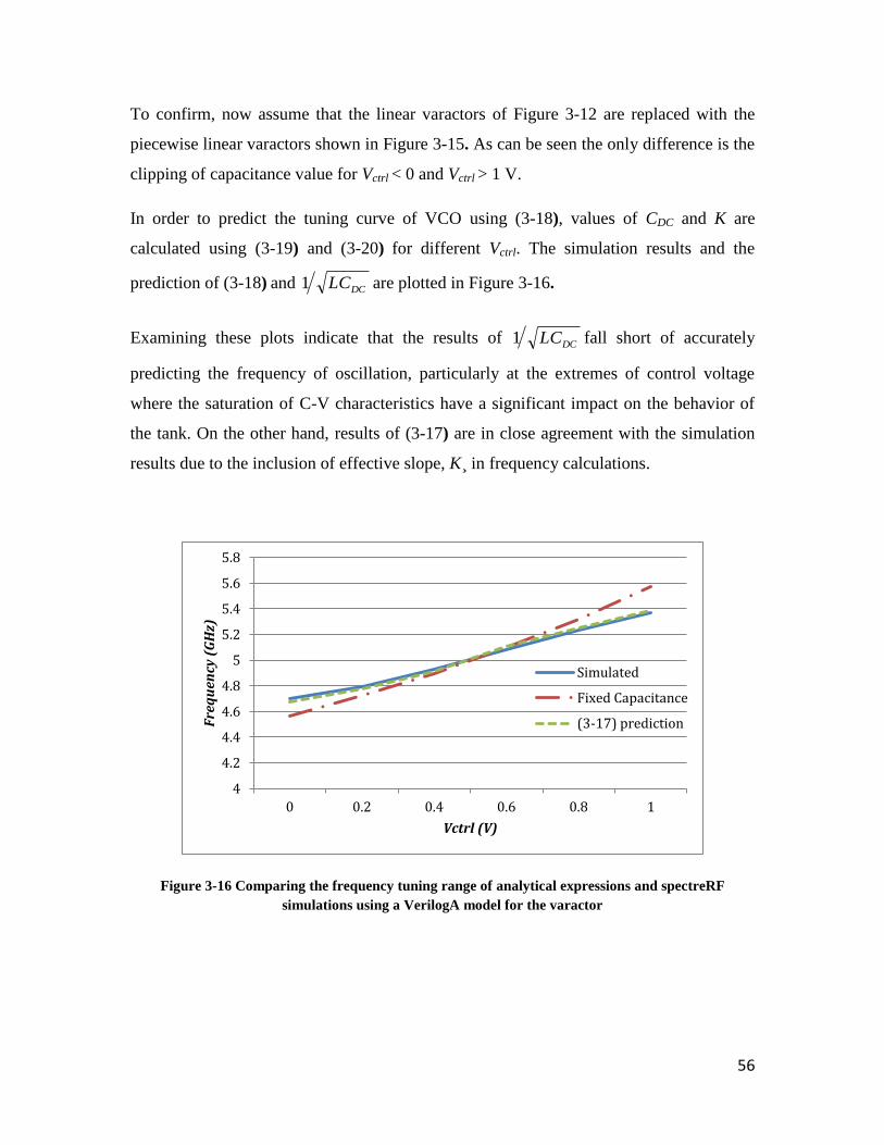
56
To confirm, now assume that the linear varactors of Figure 3-12 are replaced with the
piecewise linear varactors shown in Figure 3-15. As can be seen the only difference is the
clipping of capacitance value for Vctrl < 0 and Vctrl > 1 V.
In order to predict the tuning curve of VCO using (3-18), values of CDC and K are
calculated using (3-19) and (3-20) for different Vctrl. The simulation results and the
prediction of (3-18) and DCLC1 are plotted in Figure 3-16.
Examining these plots indicate that the results of DCLC1 fall short of accurately
predicting the frequency of oscillation, particularly at the extremes of control voltage
where the saturation of C-V characteristics have a significant impact on the behavior of
the tank. On the other hand, results of (3-17) are in close agreement with the simulation
results due to the inclusion of effective slope, K¸ in frequency calculations.
Figure 3-16 Comparing the frequency tuning range of analytical expressions and spectreRF
simulations using a VerilogA model for the varactor
4
4.2
4.4
4.6
4.8
5
5.2
5.4
5.6
5.8
0 0.2 0.4 0.6 0.8 1
Fre
qu
ency
(G
Hz)
Vctrl (V)
Simulated
Fixed Capacitance
(3-17) prediction

57
Figure 3-17 Comparing the 2nd
harmonic amplitude of analytical expressions and spectreRF
simulations using a VerilogA model
Also, plotted in Figure 3-17 are the simulated amplitude of the second harmonic as well
as that predicted by ( 3-18). The curve peaks at the middle of the control voltage because
the effective slope, K, as calculated by (3-20) is at its maximum when varactor is biased at
the center of its steep region, i.e. point C in Figure 3-15. Also, it is interesting to note that
shape of amplitude is not symmetrical around its peak. In fact, the amplitude is smaller at
the lower end of the tuning range due to larger CDC , as expected by (3-19).
This result demonstrates a principle difference between the fundamental-mode and 2nd
harmonic mode of operation. In the former, the amplitude of oscillation is determined by
the current flowing through the cross-coupled devices and is given by the formula (for
current-limited regime of operation)[60]:
IRA
2
( 3-21)
(3-21) implies that amplitude of the oscillation is not a function of control voltage and
remains constant across the frequency tuning range. On the other hand, Figure 3-17
emphasizes that the amplitude of the second harmonic is a strong function of the varactor
C-V characteristic and may vary quite substantially across the tuning range as the
0
5
10
15
20
25
30
35
40
45
0 0.2 0.4 0.6 0.8 1
2n
d H
arm
on
ic A
mp
litu
de
(m
V)
Vctrl (V)
Simulated 2nd harmonic (3-18) prediction
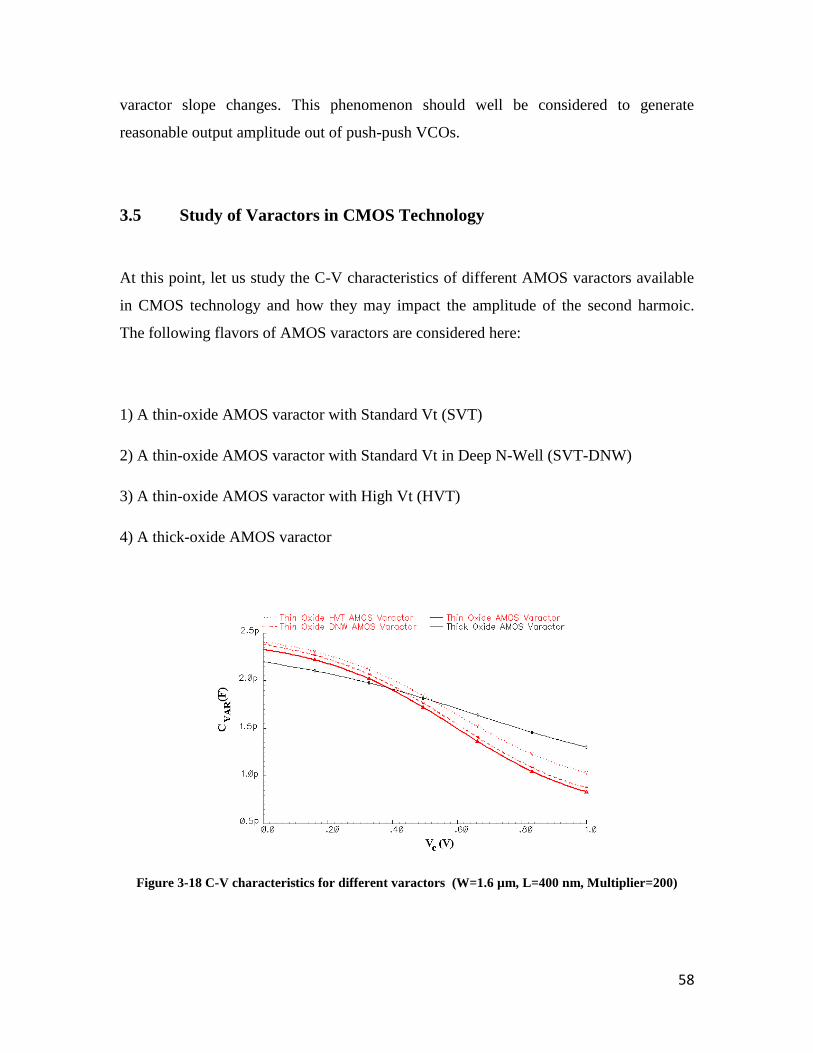
58
varactor slope changes. This phenomenon should well be considered to generate
reasonable output amplitude out of push-push VCOs.
3.5 Study of Varactors in CMOS Technology
At this point, let us study the C-V characteristics of different AMOS varactors available
in CMOS technology and how they may impact the amplitude of the second harmoic.
The following flavors of AMOS varactors are considered here:
1) A thin-oxide AMOS varactor with Standard Vt (SVT)
2) A thin-oxide AMOS varactor with Standard Vt in Deep N-Well (SVT-DNW)
3) A thin-oxide AMOS varactor with High Vt (HVT)
4) A thick-oxide AMOS varactor
Figure 3-18 C-V characteristics for different varactors (W=1.6 µm, L=400 nm, Multiplier=200)
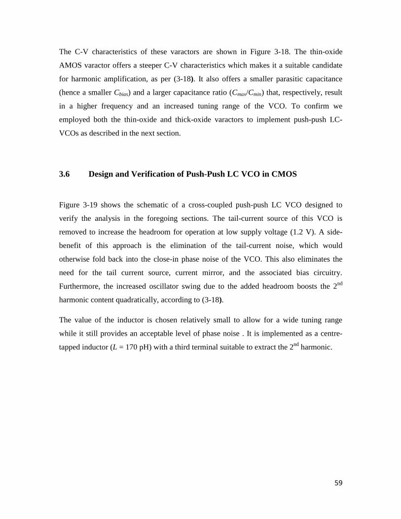
59
The C-V characteristics of these varactors are shown in Figure 3-18. The thin-oxide
AMOS varactor offers a steeper C-V characteristics which makes it a suitable candidate
for harmonic amplification, as per (3-18). It also offers a smaller parasitic capacitance
(hence a smaller Cbias) and a larger capacitance ratio (Cmax/Cmin) that, respectively, result
in a higher frequency and an increased tuning range of the VCO. To confirm we
employed both the thin-oxide and thick-oxide varactors to implement push-push LC-
VCOs as described in the next section.
3.6 Design and Verification of Push-Push LC VCO in CMOS
Figure 3-19 shows the schematic of a cross-coupled push-push LC VCO designed to
verify the analysis in the foregoing sections. The tail-current source of this VCO is
removed to increase the headroom for operation at low supply voltage (1.2 V). A side-
benefit of this approach is the elimination of the tail-current noise, which would
otherwise fold back into the close-in phase noise of the VCO. This also eliminates the
need for the tail current source, current mirror, and the associated bias circuitry.
Furthermore, the increased oscillator swing due to the added headroom boosts the 2nd
harmonic content quadratically, according to (3-18).
The value of the inductor is chosen relatively small to allow for a wide tuning range
while it still provides an acceptable level of phase noise . It is implemented as a centre-
tapped inductor (L = 170 pH) with a third terminal suitable to extract the 2nd
harmonic.
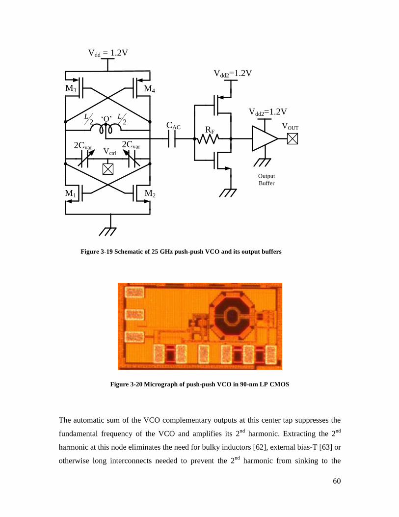
60
M3
M1
2Cvar
Output
Buffer
Vdd = 1.2V
2CvarVctrl
M4
M2
2L
Vdd2=1.2V
VOUT2
L
Vdd2=1.2V
CAC RF
‘O’
Figure 3-19 Schematic of 25 GHz push-push VCO and its output buffers
Figure 3-20 Micrograph of push-push VCO in 90-nm LP CMOS
The automatic sum of the VCO complementary outputs at this center tap suppresses the
fundamental frequency of the VCO and amplifies its 2nd
harmonic. Extracting the 2nd
harmonic at this node eliminates the need for bulky inductors [62], external bias-T [63] or
otherwise long interconnects needed to prevent the 2nd
harmonic from sinking to the
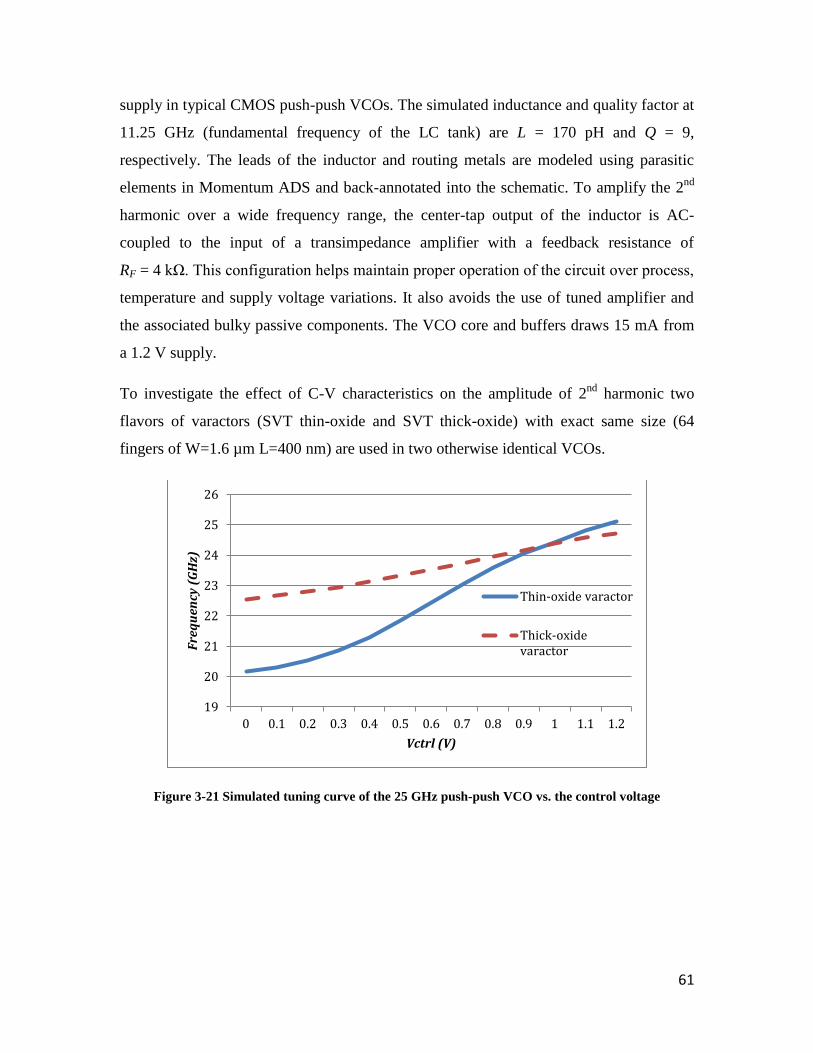
61
supply in typical CMOS push-push VCOs. The simulated inductance and quality factor at
11.25 GHz (fundamental frequency of the LC tank) are L = 170 pH and Q = 9,
respectively. The leads of the inductor and routing metals are modeled using parasitic
elements in Momentum ADS and back-annotated into the schematic. To amplify the 2nd
harmonic over a wide frequency range, the center-tap output of the inductor is AC-
coupled to the input of a transimpedance amplifier with a feedback resistance of
RF = 4 kΩ. This configuration helps maintain proper operation of the circuit over process,
temperature and supply voltage variations. It also avoids the use of tuned amplifier and
the associated bulky passive components. The VCO core and buffers draws 15 mA from
a 1.2 V supply.
To investigate the effect of C-V characteristics on the amplitude of 2nd
harmonic two
flavors of varactors (SVT thin-oxide and SVT thick-oxide) with exact same size (64
fingers of W=1.6 µm L=400 nm) are used in two otherwise identical VCOs.
Figure 3-21 Simulated tuning curve of the 25 GHz push-push VCO vs. the control voltage
19
20
21
22
23
24
25
26
0 0.1 0.2 0.3 0.4 0.5 0.6 0.7 0.8 0.9 1 1.1 1.2
Fre
qu
ency
(G
Hz)
Vctrl (V)
Thin-oxide varactor
Thick-oxide varactor

62
(a) (b)
Figure 3-22 Comparison of simulation and measurement results for the tuning curves of a) Thin-
oxide varactor b) Thick-oxide varactor
The tank oscillation at half the output clock frequency allows a broad tuning range of
20.1 GHz to 25.2 GHz at the output of VCO employing the thin-oxide varactor. The
tuning range of the VCO employing thick-oxide varactor is smaller and limited from
22.5 GHz to 24.65 GHz, as expected. The simulated tuning curve of the VCO versus the
control voltage is shown in Figure 3-21. Based on postlayout spectreRF PSS/PNOISE
simulations, the oscillator exhibits a phase noise of -101 dBc/Hz at 1 MHz offset of a
24.5 GHz output (LC tank tuned at 12.25 GHz).
3.6.1 Measurement Results
The two push-push VCOs described in the previous section are fabricated in a 90-nm
CMOS process. This VCO is targeted for K-band application when operating at the 2nd
-
harmonic frequency (push-push mode). RF transistors and inductor layouts characterized
and provided by the foundry are used. The output buffer is designed to drive the 50 Ω
impedance of the measurement device. Cascade RF-1 Microwave probe station with
Cascade RF quadrant PGSSGP probe (with power-ground-signal-signal-ground-power
pin configuration) with 100 µm pitch between its pins is used for on-die measurements.
Using the Casecade calibration substrate (ISS 101-190), and following a standard set of
short, open and load measurements the loss of probes and cables are de-embedded. The
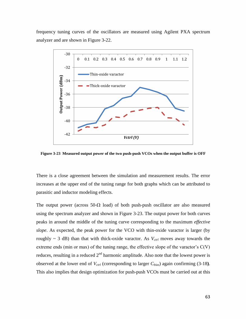
63
frequency tuning curves of the oscillators are measured using Agilent PXA spectrum
analyzer and are shown in Figure 3-22.
Figure 3-23 Measured output power of the two push-push VCOs when the output buffer is OFF
There is a close agreement between the simulation and measurement results. The error
increases at the upper end of the tuning range for both graphs which can be attributed to
parasitic and inductor modeling effects.
The output power (across 50- load) of both push-push oscillator are also measured
using the spectrum analyzer and shown in Figure 3-23. The output power for both curves
peaks in around the middle of the tuning curve corresponding to the maximum effective
slope. As expected, the peak power for the VCO with thin-oxide varactor is larger (by
roughly ~ 3 dB) than that with thick-oxide varactor. As Vctrl moves away towards the
extreme ends (min or max) of the tuning range, the effective slope of the varactor’s C(V)
reduces, resulting in a reduced 2nd
harmonic amplitude. Also note that the lowest power is
observed at the lower end of Vctrl (corresponding to larger Cbias) again confirming (3-18).
This also implies that design optimization for push-push VCOs must be carried out at this
-42
-40
-38
-36
-34
-32
-30
0 0.1 0.2 0.3 0.4 0.5 0.6 0.7 0.8 0.9 1 1.1 1.2 O
utp
ut
Po
we
r (d
Bm
)
Vctrl (V)
Thin-oxide varactor
Thick-oxide varactor
64
extreme of Vctrl to guarantee satisfactory swing levels at the output. In other words, there
is a trade-off between the tuning range and the output swing at the doubled frequency.
3.7 Low-Power Technique to Boost the Amplitude
As observed the amplitude of 2nd
harmonic generated in AMOS LC-VCOs, (3-17), is
weak and a relatively large power is required to bring it to an acceptable swing level. In
this section we show that by employing a resonance technique inside the LC tank the
amplitude of 2nd
harmonic may significantly be increased alleviating the power
consumption burden.
To show the details, consider again the LC tank of a differential VCO with a centre-
tapped inductor, as shown in Figure 3-24. In this differential structure, the fundamental
oscillation frequency of the tank (f0) appears as two voltage components in opposite
phases at nodes 'A' and 'B'. On the other hand, the 2nd
harmonic voltages at these two
nodes are in-phase [64]. Therefore, the signals from nodes 'A' and 'B' can be combined
(added up) to cancel out the fundamental component while amplifying the 2nd
harmonic
to generate a single-ended output.
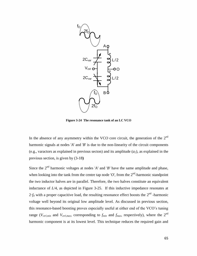
65
A
B
Vctrl
2Cvar
2Cvar
O
L / 2
L / 2
fO2fO
2fO
fO
Figure 3-24 The resonance tank of an LC VCO
In the absence of any asymmetry within the VCO core circuit, the generation of the 2nd
harmonic signals at nodes 'A' and 'B' is due to the non-linearity of the circuit components
(e.g., varactors as explained in previous secton) and its amplitude (a2), as explained in the
previous section, is given by (3-18)
Since the 2nd
harmonic voltages at nodes 'A' and 'B' have the same amplitude and phase,
when looking into the tank from the centre tap node 'O', from the 2nd
-harmonic standpoint
the two inductor halves are in parallel. Therefore, the two halves constitute an equivalent
inductance of L/4, as depicted in Figure 3-25. If this inductive impedance resonates at
2·f0 with a proper capacitive load, the resulting resonance effect boosts the 2nd
-harmonic
voltage well beyond its original low amplitude level. As discussed in previous section,
this resonance-based boosting proves especially useful at either end of the VCO’s tuning
range (Vctrl,min and Vctrl,max, corresponding to fmin and fmax, respectively), where the 2nd
harmonic component is at its lowest level. This technique reduces the required gain and
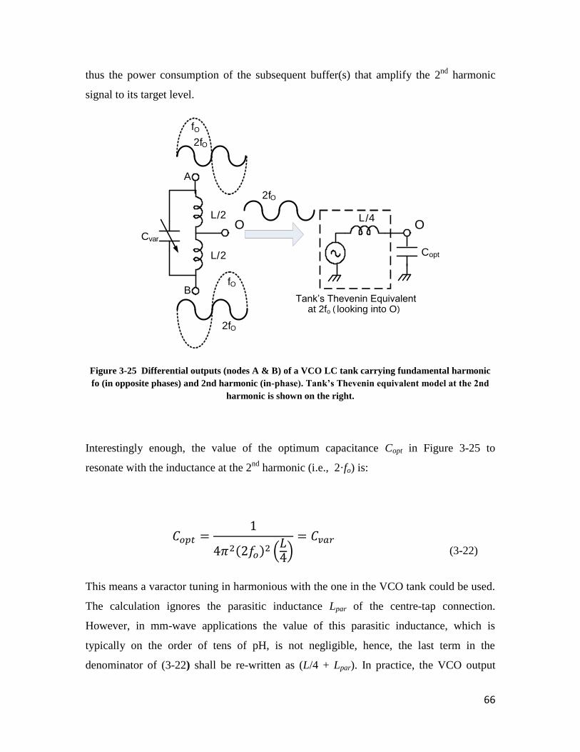
66
thus the power consumption of the subsequent buffer(s) that amplify the 2nd
harmonic
signal to its target level.
L/2
L/2
A
B
OL/4
O
Copt
2fO
fO
2fO
Tank’s Thevenin Equivalent2fo ( looking into O)at
Cvar
2fO
fO
Figure 3-25 Differential outputs (nodes A & B) of a VCO LC tank carrying fundamental harmonic
fo (in opposite phases) and 2nd harmonic (in-phase).Tank’sTheveninequivalentmodelatthe2nd
harmonic is shown on the right.
Interestingly enough, the value of the optimum capacitance Copt in Figure 3-25 to
resonate with the inductance at the 2nd
harmonic (i.e., 2·fo) is:
( 3-22)
This means a varactor tuning in harmonious with the one in the VCO tank could be used.
The calculation ignores the parasitic inductance Lpar of the centre-tap connection.
However, in mm-wave applications the value of this parasitic inductance, which is
typically on the order of tens of pH, is not negligible, hence, the last term in the
denominator of ( 3-22) shall be re-written as (L/4 + Lpar). In practice, the VCO output

67
goes through several buffering stages before driving the final load. The design of the
buffer chain, considering its impact on the VCO output, entails an optimization task,
which takes into account both the final load and the described 2nd
-harmonic resonance
effect.
Figure 3-26 (a) Large buffer transistor means large capacitance modulation that lowers the 2nd-
harmonic swing at node O, (b) Fixed capacitance plus the gate capacitance of a smaller buffer
transistor brings higher resonant swing at node O.
To explain this, consider Figure 3-26a, where the voltage swing of the 2nd
-harmonic at
the inductor’s centre tap modulates the capacitance value on this node. If the capacitive
load is mainly comprised of MOS device(s), e.g., CGS of the buffer transistor in
Figure 3-26a, the capacitance value becomes highly voltage-dependant. Thus, the
instantaneous capacitance is modulated by the voltage swing on node 'O', which in turn
causes deviation from the desired resonance frequency and results in a lower swing. In
other words, the frequency of the autonomous circuit (VCO) is determined by the main
LC tank, while that of the amplitude-resonance circuit is determined by (L/4 || Co) where
Co is the actual value of capacitance observed at node 'O'. Any deviation of the
amplitude-resonance frequency from the desired value of 2·fo would cause sub-optimum
amplification of the 2nd
-harmonic amplitude. A preferred design choice shown in
Figure 3-26b is when a large portion of the nodal capacitance Copt is not voltage-
dependent, an approach that minimizes the capacitance modulation by the voltage swing
at node 'O'. In this case, to optimize the 2nd
-harmonic-amplitude resonance a

68
programmable switch is employed to add a proper fixed capacitance, namely, a metal-
oxide-metal (MoM) capacitor, for the desired VCO frequency. It is worth noting that the
core of the LC VCO is insensitive to any load variation at the common-mode node 'O',
which is an advantage of this architecture. Thus, as discussed in the next section, one can
use an array of switched capacitors to adjust the value of this fixed capacitor.
3.8 Implementation in CMOS and Measurements
To verify the proposed 2nd
-harmonic boosting technique, a push-push VCO is designed
and implemented in a 90-nm low-power (LP) CMOS process. The core of VCO is similar
to the push-push VCO implemented in the previous section and employs a thin-oxide
varactor and a centre-tapped inductor (L = 170 pH) that generates a frequency range of
20.1 GHz to 24.8 GHz when operating at the 2nd
-harmonic frequency. The 2nd
-harmonic
voltage is tapped off the centre tap of the inductor, boosted by the proposed resonance
effect, and passed to the output through the buffer. Using an extracted RLC model of this
centre tap, the value of the additional capacitor Copt for 2nd
-harmonic resonance was
derived through simulations. The schematic of the VCO and the micrograph of the
fabricated CMOS die are shown in Figure 3-27 and Figure 3-28, respectively.
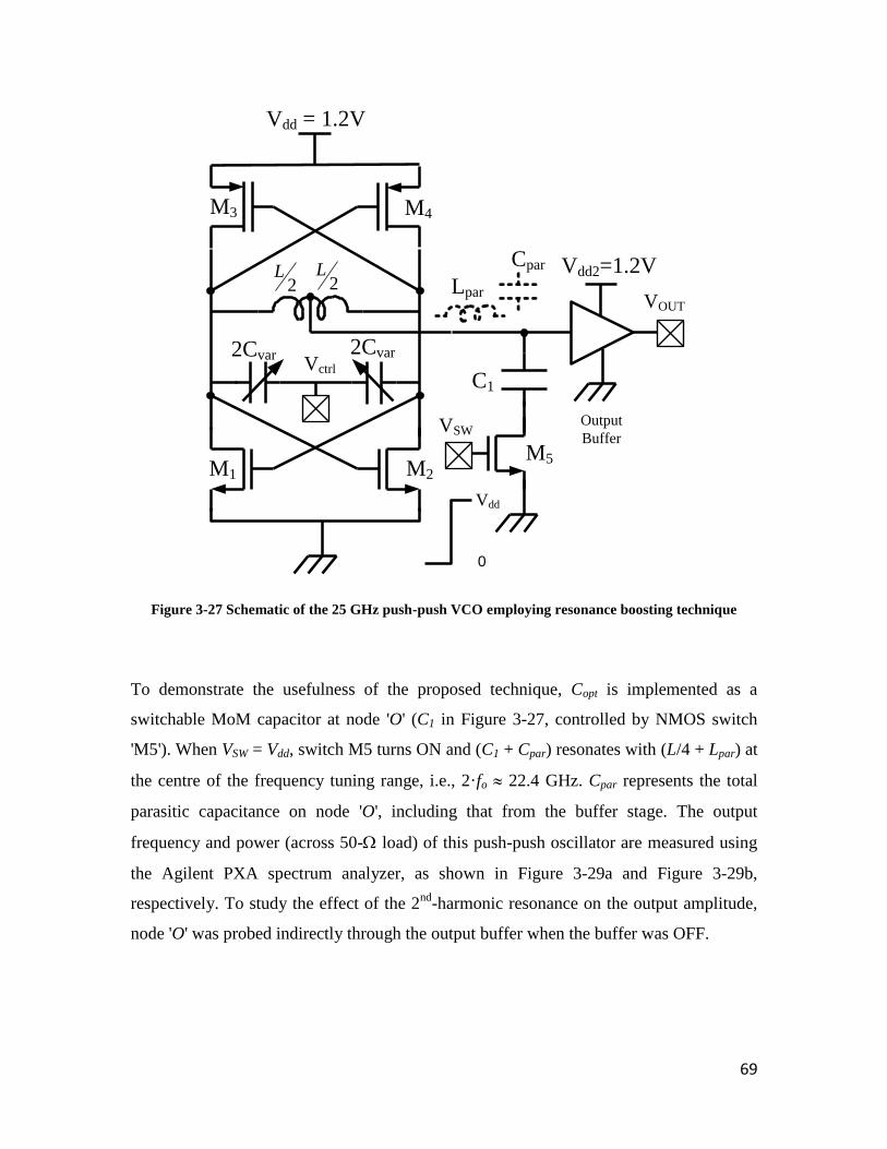
69
M5
M3
M1
Lpar
Cpar
2Cvar
Output
Buffer
Vdd = 1.2V
0
2CvarVctrl
C1
VSW
M4
M2
Vdd
2L Vdd2=1.2V
VOUT
2L
Figure 3-27 Schematic of the 25 GHz push-push VCO employing resonance boosting technique
To demonstrate the usefulness of the proposed technique, Copt is implemented as a
switchable MoM capacitor at node 'O' (C1 in Figure 3-27, controlled by NMOS switch
'M5'). When VSW = Vdd, switch M5 turns ON and (C1 + Cpar) resonates with (L/4 + Lpar) at
the centre of the frequency tuning range, i.e., 2·fo 22.4 GHz. Cpar represents the total
parasitic capacitance on node 'O', including that from the buffer stage. The output
frequency and power (across 50- load) of this push-push oscillator are measured using
the Agilent PXA spectrum analyzer, as shown in Figure 3-29a and Figure 3-29b,
respectively. To study the effect of the 2nd
-harmonic resonance on the output amplitude,
node 'O' was probed indirectly through the output buffer when the buffer was OFF.
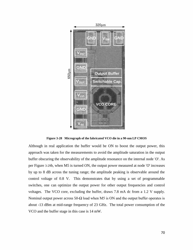
70
VCO CORE
Switchable Cap.
Output Buffer
Vctrl
VSW
320µm
65
0µ
m
Vdd
Vdd2
GND
GND
VOUT
GND GND
Figure 3-28 Micrograph of the fabricated VCO die in a 90-nm LP CMOS
Although in real application the buffer would be ON to boost the output power, this
approach was taken for the measurements to avoid the amplitude saturation in the output
buffer obscuring the observability of the amplitude resonance on the internal node 'O'. As
per Figure 3-29b, when M5 is turned ON, the output power measured at node 'O' increases
by up to 8 dB across the tuning range; the amplitude peaking is observable around the
control voltage of 0.8 V. This demonstrates that by using a set of programmable
switches, one can optimize the output power for other output frequencies and control
voltages. The VCO core, excluding the buffer, draws 7.8 mA dc from a 1.2 V supply.
Nominal output power across 50-Ω load when M5 is ON and the output buffer operates is
about -13 dBm at mid-range frequency of 23 GHz. The total power consumption of the
VCO and the buffer stage in this case is 14 mW.
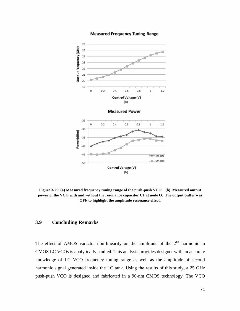
71
Figure 3-29 (a) Measured frequency tuning range of the push-push VCO, (b) Measured output
power of the VCO with and without the resonance capacitor C1 at node O. The output buffer was
OFF to highlight the amplitude resonance effect.
3.9 Concluding Remarks
The effect of AMOS varactor non-linearity on the amplitude of the 2nd
harmonic in
CMOS LC VCOs is analytically studied. This analysis provides designer with an accurate
knowledge of LC VCO frequency tuning range as well as the amplitude of second
harmonic signal generated inside the LC tank. Using the results of this study, a 25 GHz
push-push VCO is designed and fabricated in a 90-nm CMOS technology. The VCO

72
achieves a wide tuning range (100 × (fmax/fmin -1) ≈ 24.7%) while keeping an acceptable
compromise between the power consumption (18 mW) and the phase noise (-101 dBc/Hz
at 1 MHz offset from 25 GHz). The use of a compact center-tapped inductor, the removal
of bias currents, transmission lines and matching components, makes this VCO design a
compact and inexpensive solution that is attractive for System-on-Chip implementations
in general-purpose digital CMOS processes.
This chapter also proposes a technique to increase the output amplitude of the push-push
VCO by boosting the 2nd
-harmonic through an LC resonance, hence facilitating the
design of low-power-consumption VCOs [65]. Measurement results of a proof-of-
concept push-push VCO implemented in a 90-nm LP CMOS process confirm the
usefulness of this technique.
73
Chapter 4
Dense Integration of LC-VCOs and Coupling
Issues
The design of clock multipliers for multi-rate multi-standard applications involves a
trade-off between the output clock jitter and the frequency tuning range. Traditionally, a
wide range is achieved via non-LC-based oscillators such as relaxation or ring oscillators
[66-68] at the cost of higher phase noise and intrinsic jitter. LC VCOs are used for low-
jitter multi-gigahertz applications, but their tuning range is inherently small [67][69].
Moreover, dense integration of multiple LC VCOs on a silicon die poses a new challenge
due to mutual coupling between inductors and the resulting frequency pulling and
induced phase jitter among adjacent oscillators.
In this chapter we present an analytical model to study the effect of coupling between
adjacent LC VCOs when operating in a plesiochronous manner. Based on this study, a
low-jitter highly compact clock synthesizer unit supporting a continuous (gapless)
frequency range up to 5.8 GHz is designed and implemented in a 65-nm digital CMOS
process. Measurement results are presented for densely integrated PLLs verifying the
results of proposed analytical model. Finally, a redundant frequency mapping scheme is
proposed to reduce the effect of coupling amongst plesiochronously running links.
4.1 Clock Jitter in Plesiochronous Neighboring PLLs
According to ITU standards for Telecommunications (ITU-T), two signals are
plesiochronous if they have the same nominal rate, with any variation in rate being

74
(a) (b)
Figure 4-1 a)Two adjacent VCOs coupling to each other b)The current flowing through the inductor
in the aggressor VCO (Ia) generates a voltage on the tank of victim VCO (Vn,OC)
constrained within specified limits. For example, two bit streams are plesiochronous if
they are clocked off two independent clock sources that have the same nominal
frequencies but may have a slight frequency mismatch measured in parts-per-million
(ppm), which would lead to a drifting phase and cycle slips. In other words, two
plesiochronous signals or systems are almost synchronous, but not quite perfectly.
One of the most challenging situations for noise coupling among densely-integrated
SERDES links with independent rates is when adjacent links run in a plesiochronous
manner with the line rates offset by around ±10 to ±500 ppm. In this case, magnetic
coupling between LC VCOs causing noise and spurs within the bandwidth of the PLLs
proves to be problematic, especially for Telecommunication standards with close-in jitter
specifications (e.g., SONET OC-48 with jitter integration band from 12 kHz to 20 MHz).
We present a model that helps understand the behavior of the unwanted periodic jitter in
two adjacent PLLs (here known as aggressor and victim), when the two PLLs operate at a
small frequency offset and the magnetic isolation between their VCO inductors is finite.
To quantify this effect, consider two adjacent VCOs operating at slightly different
frequencies, the victim VCO at ωo and the aggressor VCO at ωa = ωo + Δω, separated by
small frequency offset Δω as shown in Figure 4-1a.
Victim
VCO
Coupling
ωo
Vn(t)
ωa
Aggressor
VCO
L1 L2C1 C2
21LL
Mk
Ia
L1 = L2 = L
+
-
Vn,OC
Aggressor Victim
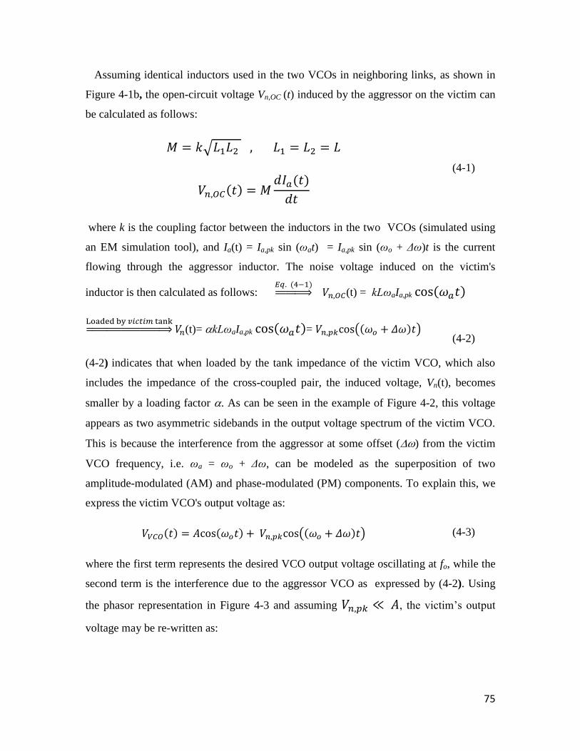
75
Assuming identical inductors used in the two VCOs in neighboring links, as shown in
Figure 4-1b, the open-circuit voltage Vn,OC (t) induced by the aggressor on the victim can
be calculated as follows:
( 4-1)
where k is the coupling factor between the inductors in the two VCOs (simulated using
an EM simulation tool), and Ia(t) = Ia,pk sin (ωat) = Ia,pk sin (ωo + Δω)t is the current
flowing through the aggressor inductor. The noise voltage induced on the victim's
inductor is then calculated as follows: (t) = kLωaIa,pk
(t)= kLωaIa,pk =
( 4-2)
( 4-2) indicates that when loaded by the tank impedance of the victim VCO, which also
includes the impedance of the cross-coupled pair, the induced voltage, Vn(t), becomes
smaller by a loading factor . As can be seen in the example of Figure 4-2, this voltage
appears as two asymmetric sidebands in the output voltage spectrum of the victim VCO.
This is because the interference from the aggressor at some offset () from the victim
VCO frequency, i.e. ωa = ωo + Δω, can be modeled as the superposition of two
amplitude-modulated (AM) and phase-modulated (PM) components. To explain this, we
express the victim VCO's output voltage as:
( 4-3)
where the first term represents the desired VCO output voltage oscillating at fo, while the
second term is the interference due to the aggressor VCO as expressed by ( 4-2). Using
the phasor representation in Figure 4-3 and assuming , the victim’s output
voltage may be re-written as:
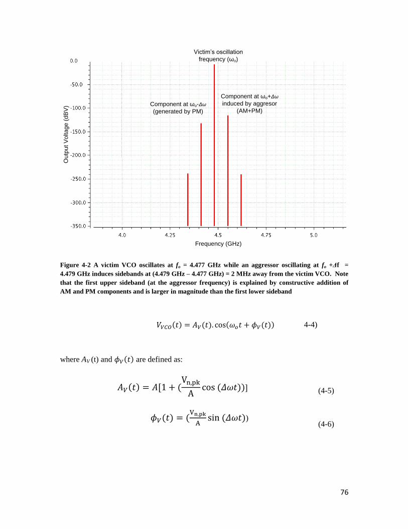
76
Victim’s oscillation
frequency (ωo)
Component at ωo+Δω
induced by aggresor
(AM+PM)Component at ωo-Δω
(generated by PM)
Frequency (GHz)
Ou
tpu
t V
olta
ge
(d
BV
)
Figure 4-2 A victim VCO oscillates at fo = 4.477 GHz while an aggressor oscillating at fo +Δf =
4.479 GHz induces sidebands at (4.479 GHz – 4.477 GHz) = 2 MHz away from the victim VCO. Note
that the first upper sideband (at the aggressor frequency) is explained by constructive addition of
AM and PM components and is larger in magnitude than the first lower sideband
4-4)
where AV (t) and are defined as:
( 4-5)
)
( 4-6)
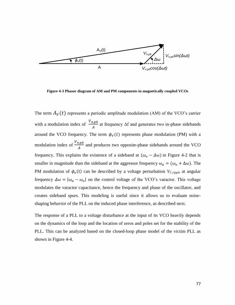
77
A
Vn,pk
Δω
Vn,pkcos(Δωt)
Vn,pksin(Δωt)
AV(t)
ɸV(t)
Figure 4-3 Phasor diagram of AM and PM components in magnetically coupled VCOs
The term represents a periodic amplitude modulation (AM) of the VCO’s carrier
with a modulation index of
at frequency Δf and generates two in-phase sidebands
around the VCO frequency. The term represents phase modulation (PM) with a
modulation index of
and produces two opposite-phase sidebands around the VCO
frequency. This explains the existence of a sideband at in Figure 4-2 that is
smaller in magnitude than the sideband at the aggressor frequency . The
PM modulation of can be described by a voltage perturbation VC,ripple at angular
frequency on the control voltage of the VCO’s varactor. This voltage
modulates the varactor capacitance, hence the frequency and phase of the oscillator, and
creates sideband spurs. This modeling is useful since it allows us to evaluate noise-
shaping behavior of the PLL on the induced phase interference, as described next.
The response of a PLL to a voltage disturbance at the input of its VCO heavily depends
on the dynamics of the loop and the location of zeros and poles set for the stability of the
PLL. This can be analyzed based on the closed-loop phase model of the victim PLL as
shown in Figure 4-4.
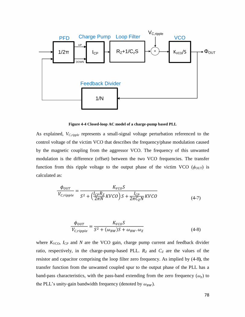
78
1/2π ICP RZ+1/CzS
1/N
UP
DOWN
KVCO/S+
VC,ripple
ΦOUT
PFD Charge Pump Loop Filter VCO
Feedback Divider
Figure 4-4 Closed-loop AC model of a charge-pump based PLL
As explained, VC,ripple represents a small-signal voltage perturbation referenced to the
control voltage of the victim VCO that describes the frequency/phase modulation caused
by the magnetic coupling from the aggressor VCO. The frequency of this unwanted
modulation is the difference (offset) between the two VCO frequencies. The transfer
function from this ripple voltage to the output phase of the victim VCO (ϕOUT) is
calculated as:
( 4-7)
( 4-8)
where KVCO, ICP and N are the VCO gain, charge pump current and feedback divider
ratio, respectively, in the charge-pump-based PLL. RZ and CZ are the values of the
resistor and capacitor comprising the loop filter zero frequency. As implied by (4-8), the
transfer function from the unwanted coupled spur to the output phase of the PLL has a
band-pass characteristics, with the pass-band extending from the zero frequency ( ) to
the PLL’s unity-gain bandwidth frequency (denoted by ).
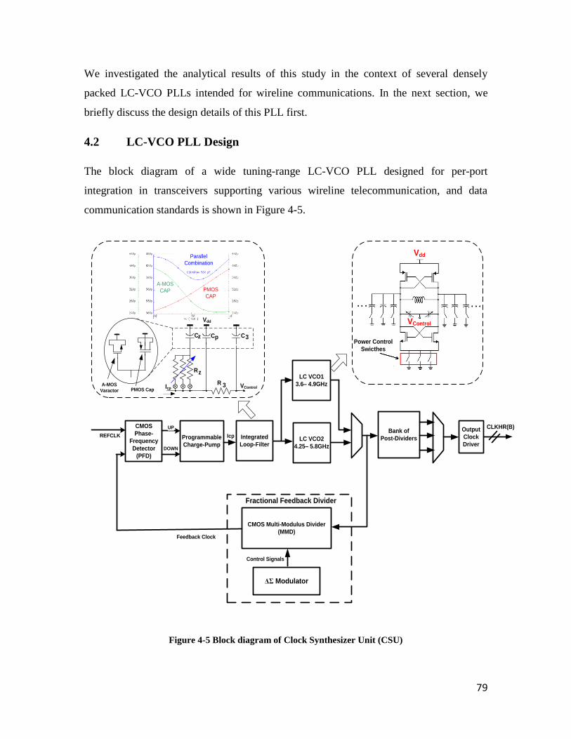
79
We investigated the analytical results of this study in the context of several densely
packed LC-VCO PLLs intended for wireline communications. In the next section, we
briefly discuss the design details of this PLL first.
4.2 LC-VCO PLL Design
The block diagram of a wide tuning-range LC-VCO PLL designed for per-port
integration in transceivers supporting various wireline telecommunication, and data
communication standards is shown in Figure 4-5.
CMOS
Phase-
Frequency
Detector
(PFD)
Programmable
Charge-Pump
Integrated
Loop-Filter
CMOS Multi-Modulus Divider
(MMD)
UP
DOWN
Output
Clock
Driver
Icp
ΔΣ Modulator
Feedback Clock
CLKHR(B)
REFCLKBank of
Post-Dividers
LC VCO1
3.6– 4.9GHz
Fractional Feedback Divider
Vdd
VControl
Power Control
Swicthes
Cp C3
Rz
R 3
Cz
VControl
Vdd
PMOS CapA-MOS
Varactor
PMOS
CAP
A-MOS
CAP
Parallel
Combination
Icp
Control Signals
LC VCO2
4.25– 5.8GHz
Figure 4-5 Block diagram of Clock Synthesizer Unit (CSU)
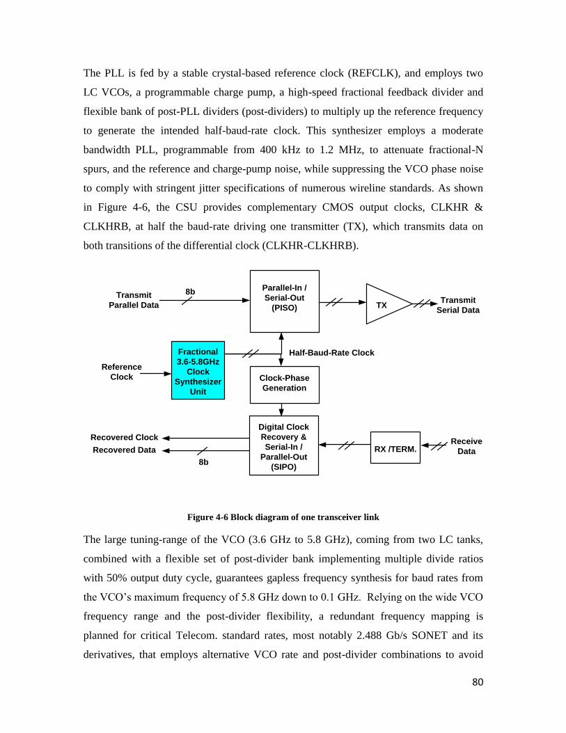
80
The PLL is fed by a stable crystal-based reference clock (REFCLK), and employs two
LC VCOs, a programmable charge pump, a high-speed fractional feedback divider and
flexible bank of post-PLL dividers (post-dividers) to multiply up the reference frequency
to generate the intended half-baud-rate clock. This synthesizer employs a moderate
bandwidth PLL, programmable from 400 kHz to 1.2 MHz, to attenuate fractional-N
spurs, and the reference and charge-pump noise, while suppressing the VCO phase noise
to comply with stringent jitter specifications of numerous wireline standards. As shown
in Figure 4-6, the CSU provides complementary CMOS output clocks, CLKHR &
CLKHRB, at half the baud-rate driving one transmitter (TX), which transmits data on
both transitions of the differential clock (CLKHR-CLKHRB).
Parallel-In /
Serial-Out
(PISO)
TX Transmit
Serial Data
Transmit
Parallel Data
Fractional
3.6-5.8GHz
Clock
Synthesizer
Unit
Reference
Clock Clock-Phase
Generation
Digital Clock
Recovery &
Serial-In /
Parallel-Out
(SIPO)
Receive
DataRX /TERM.
Recovered Clock
Recovered Data
Half-Baud-Rate Clock
8b
8b
Figure 4-6 Block diagram of one transceiver link
The large tuning-range of the VCO (3.6 GHz to 5.8 GHz), coming from two LC tanks,
combined with a flexible set of post-divider bank implementing multiple divide ratios
with 50% output duty cycle, guarantees gapless frequency synthesis for baud rates from
the VCO’s maximum frequency of 5.8 GHz down to 0.1 GHz. Relying on the wide VCO
frequency range and the post-divider flexibility, a redundant frequency mapping is
planned for critical Telecom. standard rates, most notably 2.488 Gb/s SONET and its
derivatives, that employs alternative VCO rate and post-divider combinations to avoid

81
running adjacent VCOs at the same (or close) nominal rates. This allows dense
integration of a large number of serializer-deserializer (SERDES) links each with a per-
port frequency synthesizer, without any significant inductor coupling amongst adjacent
VCOs. The CSU feedback path consists of a high-speed multi-modulus divider (MMD)
running at the VCO rate that is controlled by a ΔΣ modulator (DSM) [70][71]. The 24b
DSM uses a 3rd-order single-loop topology, allowing frequency synthesis resolution
down to 2 parts-per-billion (ppb). A programmable integrated passive loop filter is used
to suppress the reference clock and the DSM quantization noise from the VCO’s control
voltage. A parallel combination of accumulation-mode (AMOS) varactors and PMOS
capacitors is used to linearize the C-V characteristics of the on-chip capacitor to maintain
optimal loop dynamics across the range of VCO’s control voltage Vcontrol (see Figure
4-5, inset).
Two LC VCOs with overlapping tuning ranges, each comprised of a cross-coupled
NMOS and PMOS topology, generate the required 3.6 GHz to 5.8 GHz tuning range.
Integrated inductor two stacked metal layers is used to achieve high quality factor (Q)
and hence low VCO phase noise (see Chapter 2) . To increase the headroom for low-
voltage operation on 1-Volt supply, the tail current source of the VCO is eliminated.
It is worth noting that since there is no tail current source in this design, the gm of the
devices and hence the total negative resistance is solely governed by the size of the
NMOS and PMOS transistors. To guarantee the oscillation, it is necessary that RP ≥ |-
1/gm| across the frequency band, where RP is the equivalent shunt resistance of the
inductor’s series loss resistance (Rs), and gm is the overall transconductance of the cross-
coupled transistors. Assuming a relatively constant Rs vs. frequency, the minimum
required transconductance for oscillation varies by a factor of (fmax/fmin)2 across the
frequency range of each VCO. Since the gm of the cross-coupled pairs has to be large
enough to guarantee the oscillation start-up at the lower end of the frequency band, there
is a waste of power at the higher end of the frequency range, especially at Fast process
corner (FF), where the transistor threshold voltages are smaller. To alleviate this problem,
a set of programmable parallel switches control the total resistance to ground, and hence
the VCO’s power consumption (Figure 4-5, inset). This flexible scheme results in up to

82
30% power reduction for high-frequency settings or Fast silicon process corner. The wide
tuning range of the VCO is achieved through the combination of coarse tuning using
fixed switchable capacitors, implemented by a stack of interdigitated metal capacitors,
and fine tuning of the AMOS varactors via the control voltage. A VCO calibration
scheme which sets Vctrl to one of multiple voltage levels at startup (nominally Vdd/2)
selects the optimum metal capacitor for the target rate and given process corner.
Provisions have been made for temperature-aware calibration, i.e. to choose Vctrl for the
calibration based on the calibration temperature, to offer additional margin for post-
calibration variations of temperature and supply voltage.
The use of a dedicated flip-chip power bump near the VCO core is intended to minimize
IR drop and power supply noise caused by other blocks in the SERDES, including
adjacent PLLs. To further stabilize the VCO’s supply, a large decoupling capacitor,
consisting of AMOS varactor and metal capacitor using metal layers M1-M2, is
implemented underneath the patterned-ground shield (PGS) of the VCO’s inductor. The
PGS is implemented in a higher metal layer (M3) to allow this implementation. The
incremental effect on the inductor quality factor is negligible, while a large area of silicon
die is reused to filter the sensitive VCO supply.
4.3 Clock Jitter Measurement in Plesiochronous Neighboring PLLs
Figure 4-7 plots the transfer function of (4-8) for the PLL described in the previous
section. The shape of this transfer function implies that the plesiochronous links with rate
offsets close to the bandwidth of the PLL have the largest impact on one another.

83
Figure 4-7 Transfer function of the spur generated at the output of PLL
To support this analysis and key conclusion, an experiment is carried out in which the
frequency offset between two adjacent PLLs is varied from 0 (synchronous operation) to
values larger than the bandwidth of each PLL. The Total RMS Jitter (TJrms) of the PLL is
measured in the time-domain for each offset case using an oscilloscope (the RMS jitter
value is the 1-sigma of the clock jitter with a Gaussian distribution histogram) and the
results are plotted as in Figure 4-8. The PLL under test has its zero frequency and
bandwidth set to 90 kHz and 300 kHz, respectively. As seen in Figure 4-8, the total RMS
jitter peaks around 200 kHz (that is near the transfer function peaking predicted by the
transfer function of Figure 4-7 and drops off at frequencies below the zero frequency and
above the bandwidth of the PLL, as expected from (4-8).
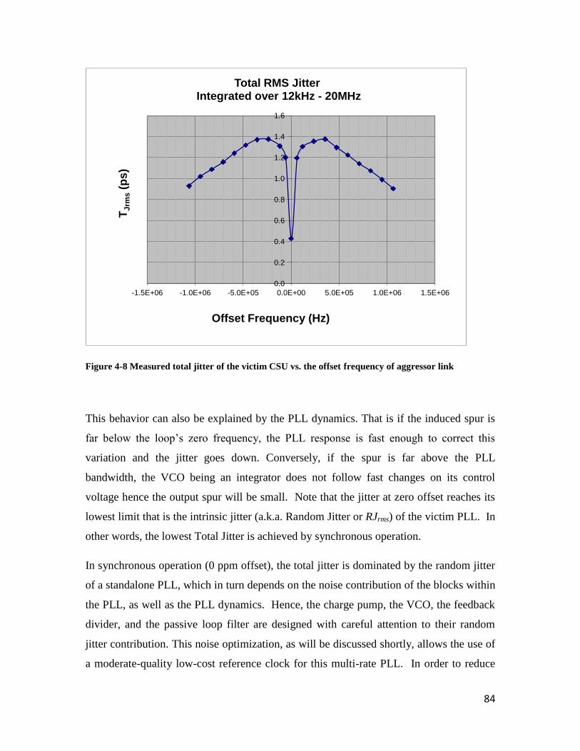
84
Figure 4-8 Measured total jitter of the victim CSU vs. the offset frequency of aggressor link
This behavior can also be explained by the PLL dynamics. That is if the induced spur is
far below the loop’s zero frequency, the PLL response is fast enough to correct this
variation and the jitter goes down. Conversely, if the spur is far above the PLL
bandwidth, the VCO being an integrator does not follow fast changes on its control
voltage hence the output spur will be small. Note that the jitter at zero offset reaches its
lowest limit that is the intrinsic jitter (a.k.a. Random Jitter or RJrms) of the victim PLL. In
other words, the lowest Total Jitter is achieved by synchronous operation.
In synchronous operation (0 ppm offset), the total jitter is dominated by the random jitter
of a standalone PLL, which in turn depends on the noise contribution of the blocks within
the PLL, as well as the PLL dynamics. Hence, the charge pump, the VCO, the feedback
divider, and the passive loop filter are designed with careful attention to their random
jitter contribution. This noise optimization, as will be discussed shortly, allows the use of
a moderate-quality low-cost reference clock for this multi-rate PLL. In order to reduce
0.0
0.2
0.4
0.6
0.8
1.0
1.2
1.4
1.6
-1.5E+06 -1.0E+06 -5.0E+05 0.0E+00 5.0E+05 1.0E+06 1.5E+06
TJrm
s (
ps
)
Offset Frequency (Hz)
Total RMS Jitter Integrated over 12kHz - 20MHz
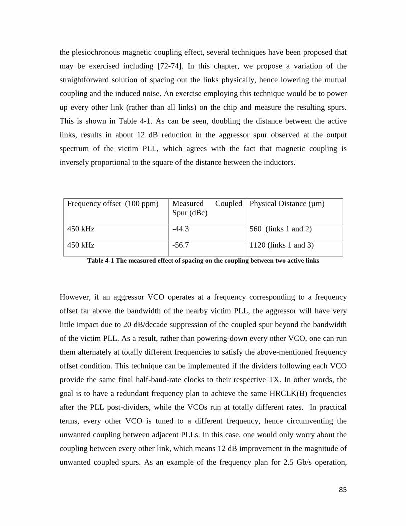
85
the plesiochronous magnetic coupling effect, several techniques have been proposed that
may be exercised including [72-74]. In this chapter, we propose a variation of the
straightforward solution of spacing out the links physically, hence lowering the mutual
coupling and the induced noise. An exercise employing this technique would be to power
up every other link (rather than all links) on the chip and measure the resulting spurs.
This is shown in Table 4-1. As can be seen, doubling the distance between the active
links, results in about 12 dB reduction in the aggressor spur observed at the output
spectrum of the victim PLL, which agrees with the fact that magnetic coupling is
inversely proportional to the square of the distance between the inductors.
Frequency offset (100 ppm) Measured Coupled
Spur (dBc)
Physical Distance (µm)
450 kHz -44.3 560 (links 1 and 2)
450 kHz -56.7 1120 (links 1 and 3)
Table 4-1 The measured effect of spacing on the coupling between two active links
However, if an aggressor VCO operates at a frequency corresponding to a frequency
offset far above the bandwidth of the nearby victim PLL, the aggressor will have very
little impact due to 20 dB/decade suppression of the coupled spur beyond the bandwidth
of the victim PLL. As a result, rather than powering-down every other VCO, one can run
them alternately at totally different frequencies to satisfy the above-mentioned frequency
offset condition. This technique can be implemented if the dividers following each VCO
provide the same final half-baud-rate clocks to their respective TX. In other words, the
goal is to have a redundant frequency plan to achieve the same HRCLK(B) frequencies
after the PLL post-dividers, while the VCOs run at totally different rates. In practical
terms, every other VCO is tuned to a different frequency, hence circumventing the
unwanted coupling between adjacent PLLs. In this case, one would only worry about the
coupling between every other link, which means 12 dB improvement in the magnitude of
unwanted coupled spurs. As an example of the frequency plan for 2.5 Gb/s operation,
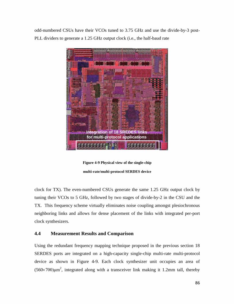
86
odd-numbered CSUs have their VCOs tuned to 3.75 GHz and use the divide-by-3 post-
PLL dividers to generate a 1.25 GHz output clock (i.e., the half-baud rate
Integration of 18 SREDES links
for multi-protocol applications
Figure 4-9 Physical view of the single-chip
multi-rate/multi-protocol SERDES device
clock for TX). The even-numbered CSUs generate the same 1.25 GHz output clock by
tuning their VCOs to 5 GHz, followed by two stages of divide-by-2 in the CSU and the
TX. This frequency scheme virtually eliminates noise coupling amongst plesiochronous
neighboring links and allows for dense placement of the links with integrated per-port
clock synthesizers.
4.4 Measurement Results and Comparison
Using the redundant frequency mapping technique proposed in the previous section 18
SERDES ports are integrated on a high-capacity single-chip multi-rate multi-protocol
device as shown in Figure 4-9. Each clock synthesizer unit occupies an area of
(560700)μm2, integrated along with a transceiver link making it 1.2mm tall, thereby
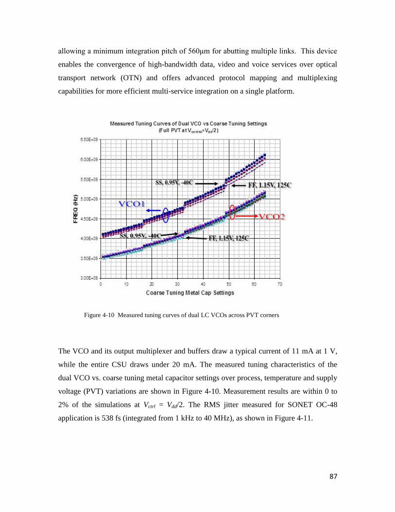
87
allowing a minimum integration pitch of 560μm for abutting multiple links. This device
enables the convergence of high-bandwidth data, video and voice services over optical
transport network (OTN) and offers advanced protocol mapping and multiplexing
capabilities for more efficient multi-service integration on a single platform.
Figure 4-10 Measured tuning curves of dual LC VCOs across PVT corners
The VCO and its output multiplexer and buffers draw a typical current of 11 mA at 1 V,
while the entire CSU draws under 20 mA. The measured tuning characteristics of the
dual VCO vs. coarse tuning metal capacitor settings over process, temperature and supply
voltage (PVT) variations are shown in Figure 4-10. Measurement results are within 0 to
2% of the simulations at Vctrl = Vdd/2. The RMS jitter measured for SONET OC-48
application is 538 fs (integrated from 1 kHz to 40 MHz), as shown in Figure 4-11.

88
Figure 4-11 Closed-loop phase noise and RMS jitter measurement at 1.244 GHz output (FVCO =
4.976 GHz); RJ=538 fs,rms (1 kHz to 40 MHz) using a signal source analyzer (SSA)
Note that the PLL’s reference clock is the dominant phase noise contributor below 1 kHz.
Despite the low output jitter of the CSU, its input reference clock has fairly relaxed
requirements for most applications. The reference clock comes from a low-cost 2-psrms
(12 kHz to 20 MHz) source, enters the chip through a single-ended pad and is
conveniently auto-routed through the digital core to all the links.

89
STANDARD
DATA
RATE
(Mb/s)
VCO
Frequency
(MHz)
Post-PLL
Divider
Ratio
RJps-rms
Isolated
channel
RJps-rms
All
channels
active
Integration
Band
Fibre Channel
FC_400 4250 4250 2 0.47 0.49
2.55 MHz to
2.125 GHz
Ethernet XAUI 3125 3906 2.5 0.48 0.55 1.87MHz to
1.556GHz
SONET OC-48 2488.32
4976.64 22 0.45 0.49 12 kHz to
20 MHz 3732.48 31 0.47 0.51
Table 4-2 Summary of the CSU clock jitter for selected wireline standards
Table 4-2 summarizes measured RMS jitter of the CSU output for a few supported
wireline standards. Comparative measurements are first presented for on an isolated link-
under-test and then for full activity on all links. Also, both alternative configurations for
odd and even channels are shown for the SONET OC-48 case. Table 4-3 presents the
performance summary and comparison with prior art.
4.5 Conclusions
The design and integration of an array of LC-based clock synthesizers for multiple
transceiver links supporting various wireline standards requires particular attention to the
issue of electromagnetic coupling amongst LC VCOs. This work develops a modeling
technique that explains the behavior of a victim synthesizer PLL due to this coupling
effect. In addition, a highly packable clock synthesizer, employing redundant frequency
mapping, is designed and fabricated in 65-nm CMOS technology. The measured clock
jitter of this synthesizer is only 0.5 ps,rms (integrated from 12 kHz to 20 MHz) in
SONET OC-48 application [78] when all adjacent links are up and running in a
plesiochronous manner that is the worst-case scenario for noise coupling.
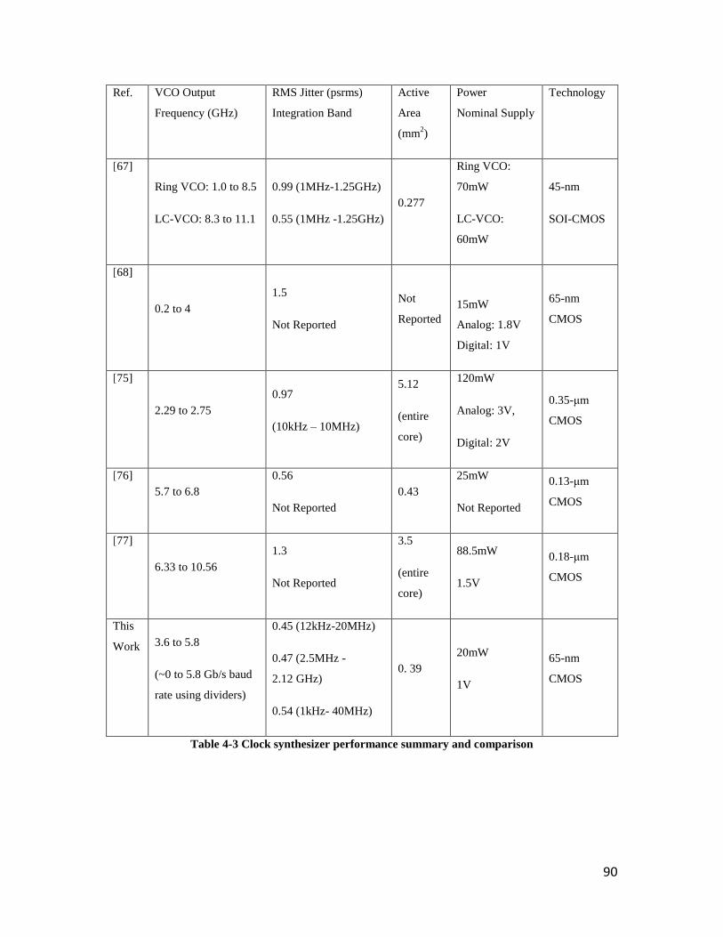
90
Ref. VCO Output
Frequency (GHz)
RMS Jitter (psrms)
Integration Band
Active
Area
(mm2)
Power
Nominal Supply
Technology
[67]
Ring VCO: 1.0 to 8.5
LC-VCO: 8.3 to 11.1
0.99 (1MHz-1.25GHz)
0.55 (1MHz -1.25GHz)
0.277
Ring VCO:
70mW
LC-VCO:
60mW
45-nm
SOI-CMOS
[68]
0.2 to 4
1.5
Not Reported
Not
Reported
15mW
Analog: 1.8V
Digital: 1V
65-nm
CMOS
[75]
2.29 to 2.75
0.97
(10kHz – 10MHz)
5.12
(entire
core)
120mW
Analog: 3V,
Digital: 2V
0.35-μm
CMOS
[76]
5.7 to 6.8
0.56
Not Reported
0.43
25mW
Not Reported
0.13-μm
CMOS
[77]
6.33 to 10.56
1.3
Not Reported
3.5
(entire
core)
88.5mW
1.5V
0.18-μm
CMOS
This
Work 3.6 to 5.8
(~0 to 5.8 Gb/s baud
rate using dividers)
0.45 (12kHz-20MHz)
0.47 (2.5MHz -
2.12 GHz)
0.54 (1kHz- 40MHz)
0. 39
20mW
1V
65-nm
CMOS
Table 4-3 Clock synthesizer performance summary and comparison
91
Chapter 5
Conclusions and Future Work
LC-VCOs are currently one of the most critical blocks in the design of high-speed clock
synthesizers. In this dissertation, we proposed solutions at the device, circuit and system
levels to address issues confronting designers in the design and integration of LC-VCOs.
In the next section, we summarize the key accomplishments presented in previous
chapters.
5.1. Accomplishments
5.1.1. Analytical Models and Expressions for Several Passive Inductor
Structures
We designed, simulated and measured several inductor structures in CMOS technology.
It is shown that the popular structures of doubly-stacked and helical inductor can be
modeled as several inductors either in parallel (former structure) or series (the latter).
Using a well-known formula for lateral inductors, a closed-form expression (5-1) for
helical inductor is suggested and later employed to design series peaking circuit at the
input of a receiver:
rnmL 22
0
( 5-1)
Also, the inductance and quality factor of coupled rings are studied from a circuit
perspective. It is shown that knowledge of coupling factor, k, is sufficient to estimate the
metrics of the structure using (5-2)
92
2
2
1
2
11
1.),1(
k
kQQkLL eqeq
( 5-2)
To complete the discussion, analytical expressions for the coupling factor of coupled
rings is proposed ((5-3)and (5-4))
21
212 2
,)]()().2
1[(2
RR
RREKk
( 5-3)
))(11( 2
1
2
2
1
R
R
R
Rk
( 5-4)
Measurement results of coupled ring test structures in CMOS are presented to verify the
findings of the analysis. The expressions presented here, are independent of the
fabrication technology and can be used in any DSM CMOS technology.
During this study, we also studied the de-embedding techniques for the inductor
characterization. The effect of undesired components is eliminated following a set of de-
embedding steps allowing for an accurate characteristics derivation of the actual device-
under-test (DUT).
Performance evaluation and comparison of variable passive inductor structures such as
coupled rings with the active inductor topologies is of utmost importance. Design of
tunable RF integrated circuits at mm-wave requires careful attention to several
parameters. Depending on the circuit block and the required performance, either active or
passive integrated inductors may be a suitable candidate for each application

93
5.1.2 Second Harmonic Signal Generation and Amplification in LC-VCOs
Employing AMOS Varactor
In this work we focused on the effect of C-V characteristics of AMOS varactors on the
differential equation governing the behavior of an LC -VCO tank. First, using a linear
approximation for the C-V characteristics of AMOS varactor and Fourier series
expansion of differential equation, we obtained the expression in (5-5) and (5-6) for the
frequency of oscillation and the amplitude of second harmonic in VCO
biasC
AKa
3
. 2
2
( 5-5)
)6
(
1
22
bias
biasC
AKCL
( 5-6)
Then, by introducing the equivalent slope and DC capacitance the analytical results are
extended to include the effects of a piecewise linear C-V characteristics. Simulation
results using VerilogA models for AMOS varactors verify the accuracy of proposed
technique.
Next, a low-power technique to boost the amplitude of the second harmonic in push-push
LC VCOs is introduced. This technique benefits from the fact that second harmonic
signals appear as in-phase component in differential LC VCOs. Extracted at the center
tap of a differential inductor, this component is significantly amplified by the addition of
a varactor tuned in harmonious with the tank varactor.
A proto-type push-push LC VCO using switched capacitors is designed and fabricated in
90-nm LP CMOS process to test the applicability the proposed technique. This LC-VCO
employed at its second harmonic covers a wide frequency tuning range of
94
20.1 - 24.8 GHz. As much as 8 dB of signal amplification is observed across the tuning
curve of the test VCO.
Employing the characteristics of passive components such as AMOS varactors to create
higher-order harmonic signals in LC-VCOs can be an interesting topic of future studies.
The analytical framework developed in this work was focused on the study of push-push
VCOs hence limiting to the second-order non-linear effects. For example, it can be
shown that the second-order non-linearity in the C-V characteristics of AMOS varactor
can contribute to the generation of third-order harmonics in LC-VCO (note that third-
order harmonic may also be created by other non-linear effects such as supply clipping).
Employing LC-VCOs to produce higher order harmonics can greatly benefit the
development of mm-wave and high-frequency oscillators developed in CMOS
5.1.3 Coupling Analysis for Plesiochronous Neighboring PLLs
We studied the effect of two neighboring PLLs coupling to one another from an
analytical standpoint. We showed that the effect of magnetic coupling from an adjacent
oscillator can be modeled as the superposition of two AM and PM spurious components
on the victim VCO. Modeling the PM component as a small perturbation on the control-
voltage of a VCO locked in a PLL loop, we showed that the magnitude of spur is
governed by the shape of band-pass transfer function presented in ( 5-7)
( 5-7)
The measurement results of several densely packed LC-oscillators in a single-chip multi-
rate SERDES device are used to verify the proposed analysis. It is shown that for two
neighboring links the lowest output jitter is achieved in synchronous operation, i.e. two
links running at exactly the same rate, each only exhibiting their respective intrinsic jitter.
95
Also, for plesichronous neighboring PLLs a redundant frequency mapping scheme is
presented which virtually doubles the distance between such neighboring links. This
technique results in 12dB reduction of the spur magnitude induced by an aggressor VCO.
Given the rapid growth of wireline communication and the need for the integration of
many serial links on a single chip the study of electromagnetic coupling amongst
densely-packed LC oscillators continue to be a topic of research in CMOS IC design.
Intelligent frequency planning as well as creative circuit design techniques that mitigate
the coupling issue allow for sustainable development of reliable high-speed data links.
The development of frequency mapping techniques and analytical models to study the
coupling issues are the essential ingredients of designing the emerging multi-standard
wireless and wireline transceivers. Also, the introduction of 3-dimensional integrated
circuits, a.k.a. 3D ICs, requires careful attention to the issue of coupling among circuit
blocks integrated in the vertical dimension.
96
References
[1] K. Chuang et al, “A 90nm CMOS Broadband Multi-Mode Mixed-Signal
Demodulator for 60GHz Radios,” IEEE Transaction on Microwave Theory and
Techniques, Vol. 58, Issue 12, pp. 4060-4071, 2010.
[2] B. Razavi, “Prospects of CMOS technology for high-speed optical communication
circuit,” Journal of Solid-State Circuits, Vol. 37, Issue 9, pp. 1135-1145, 2002.
[3] R.J Fontana, “Recent applications of short-pulse ultra-wideband,” IEEE Transaction
on Microwave Theory and Techniques, Vol. 52, Issue 9, pp. 2087-2104, 2004.
[4] Wang Wen-Chieh et al, “The design of integrated 3-GHz to 11-GHz CMOS
transmitter for full-band ultra-wideband (UWB) applications,” Proceedings of IEEE
International Symposium on Circuits and Systems (ISCAS2008), pp. 2709-2712, 2008.
[5] IEEE Standard Letter Designations for Radar-Frequency Bands, pp 1 – 3, 2003.
[6] Park Young-Bae et al, “RF receiver chip set employing 0.13µm CMOS technology
for application to K-band commercial automotive radar system,” Proceedings of
International Conference on SoC Design, pp. 146-149, 2008.
[7] Kong LingKai, E. Alon, “A 21.5mW 10+Gb/s mm-Wave phased-array transmitter in
65nm CMOS,” Proceedings of International Symposium on VLSI Circuits, pp. 52-53,
2012.
[8] A. Tomkins et al, “A Zero-IF 60 GHz 65 nm CMOS Transceiver With Direct BPSK
Modulation Demonstrating up to 6 Gb/s Data Rates Over a 2 m Wireless Link,” IEEE
Journal of Solid-State Circuits, vol. 44 , Issue 8, pp. 2085-2099, 2009.
[9] Lu Jianhua , Wang Ning-Yi, M.C.F. Chang, “A Compact and Low Power 5–10 GHz
QuadratureLocal Oscillator for Cognitive Radio Applications,” IEEE Journal of Solid-
State Circuits, vol. 47 , Issue 5, pp. 1131-1140, 2012.
[10] B. Fahs, W.Y Ali-Ahmad, P. Gamand, “A Two-Stage Ring Oscillator in 0.13-
CMOS for UWB Impulse Radio,” IEEE Transactions on Microwave Theory and
Techniques, vol. 57 , Issue 5 , pp 1074-1082, 2009.
[11] B. Razavi, RF microelectronics, Prentice Hall, 1998.
[12] Chien Jun-Chau, Lu Liang-Hung, “Design of Wide-Tuning-Range Millimeter-Wave
CMOS VCO With a Standing-Wave Architecture,” IEEE Journal of Solid-State Circuits,
vol. 42, Issue 9, pp 1942 -1952, Sep. 2007.

97
[13] V. Giannini et al, “A 2-mm 0.1–5 GHz Software-Defined Radio Receiver in 45-nm
Digital CMOS,” IEEE Journal of Solid-State Circuits, vol. 44 , Issue 12, pp. 3486-3498,
2009.
[14] K. Muhammad, “The First Fully Integrated Quad-Band GSM/GPRS Receiver in a
90-nm Digital CMOS Process,” IEEE Journal of Solid-State Circuits, vol. 41 , pp. 1772-
1780,2006.
[15] C.C. Boon et al, “A 1.2 V 2.4 GHz low spur CMOS PLL synthesizer with a gain
boosted charge pump for a batteryless transceiver,” Proceedings of IEEE International
Symposium on Radio-Frequency Integration Technology (RFIT), pp. 222-224, 2012.
[16] G. Li Puma et al, “Integration of a SiP for GSM/EDGE in CMOS Technology,”
Digest of Technical Papers. IEEE International Solid-State Circuits Conference, pp. 210
– 608, pp. 2008. ISSCC 2008.
[17] Ronald E. Reedy, M. C. Comparini, “Impact of RFIC integration of system and
subsystem blocks on MCM solutions,” European Gallium Arsenide and Other
Semiconductor Application Symposium, pp. 181-184, EGAAS 2005.
[18] J. Craninckx, M. Steyaert, “A 1.8-GHz low-phase-noise spiral-LC CMOS VCO,”
Digest of Technical Papers, International Symposium n VLSI, pp. 30-31, 1996.
[19] J.R. Long, M.A. Copeland, “The modeling, characterization, and design of
monolithic inductors for silicon RF IC's,” IEEE Journal of Solid-State Circuits, Vol. 32,
Issue 3, pp. 357-369, 1997.
[20] Yun Yang-Hun, T. –Y.J. Kao, K.O. Kenneth, “Variable Inductors in CMOS for
Millimeter-Wave Applications,” IEEE Electron Device Letters, Vol. 33, Issue 7, pp.
1081-1083, 2012.
[21] A. M. Niknejad and R. G. Meyer, “Analysis, design, and optimizationof spiral
inductors and transformers for Si RF ICs,” IEEE J. Solid-State Circuits, vol. 33, no. 10,
pp. 1470–1481, Oct. 1998.
[22] J. Borremans et al, “A Compact Wideband Front-End Using a Single-
Inductor Dual-Band VCO in 90 nm Digital CMOS,” IEEE Journal of Solid-State
Circuits, vol. 43, Issue 12, pp. 2693-2705, 2008.
[23] M.J. Uddin et al, “Design and Simulation of RF-CMOS Spiral Inductorsfor ISM
Band RFID Reader Circuits,” IEEE Workshop on Microelectronics and Electron Devices,
pp. 1-4, WMED 2009.
[24] E. Lourandakis, S. Stefanou, K. Nikellis, S. Bantas, “RF passive device modeling
and characterization in 65nm CMOS technology,” Proceedings of International
Symposium on Quality Electronic Design (ISQED), pp. 658-664, ISQED 2013.
98
[25] A.L.S. Loke et al, “A Versatile 90-nm CMOS Charge-Pump PLL for SerDes
Transmitter Clocking,” IEEE Journal of Solid-State Circuits, vol. 41, Issue 8, pp. 1894-
1907, 2006.
[26] D. Dunwell, B. Frank, “Accumulation-Mode MOS Varactors for RF CMOS Low-
Noise Amplifiers,” Proceedings of Topical Meeting on Silicon Monolithic Integrated
Circuits in RF Systems, pp. 145-148, 2007.
[27] E. Hegazi, and A. A. Abidi, “Varactor Characteristics, Oscillator Tuning Curves,
and AM-FM Conversion,” IEEE Journal of Solid-State Circuits, vol. 38, no. 6, pp. 1033-
1039, June 2003.
[28] R. L. Bunch, S. Raman, “Large-signal Analysis of MOS Varactors in CMOS – Gm
LC VCOs,” IEEE Journal of Solid-State Circuits, vol. 38, no. 8, pp. 1325-1332, August
2003.
[29] Z. Chen et al, “Fabrication and integration of high performance mixed-signal and RF
passive components in 0.13µm Cu BEOL technologies,” Proceedings of 7th international
conference on Solid-state and Integrated Circuit Technologies, vol. 1, pp. 175-178, 2004.
[30] M. Drakaki, A. Hatzopoulos, A. Siskos, “CMOS Inductor Performance Estimation
using Z- and S-parameters,” Proceedings of Int’l Symp. on Circ. & Sys. (ISCAS), pp.
2256-225, 2007.
[31] Tang Chih-Chun, Wu Chia-Hsin,Liu Shin Iuan, “Miniature 3D Inductors in Standard
CMOS Process,” IEEE Journal of Solid-State Circuits, vol. 37, no. 4, pp. 471-480, 2002.
[32] T.H. Lee, The Design of CMOS Radio-Frequency Integrated Circuits (RFIC),
Second Edition, Cambridge Press, 2004.
[33] T. Hirano et. al, “Accuracy investigation of the de-embedding technique using open
and short patterns for on-wafer RF characterization,” IEEE Asia-Pacific Microwave
Conference Proceedings (APMC), pp. 1436-1439, 2010.
[34] S. Shekhar, J.S. Walling, D.J. Allstot, “Bandwidth Extension Techniques for CMOS
Amplifiers,” IEEE Journal of Solid-State Circuits, vol. 41, Issue 11, pp 2424-2439, 2004
[35] T.H. Huang and J.-L. Wang, “New frequency plan and reconfigurable 6.6/7.128
GHz CMOS quadrature VCO for MB-OFDM UWB application,” IEEE MTT-S Int.
Microwave Symp. Dig., pp. 843–846, 2007.
[36] A. Nieuwoudt and Y. Massoud, “Optimizing the design of tunable spiral inductors
for on-chip wireless applications,” Proc. IEEE Wireless and Microwave Technology
Conf., pp. 1–5, Dec. 2006.
99
[37] M. Kossel et. al, “LC PLL With 1.2-Octave Locking Range Based on Mutual-
Inductance Switching in 45-nm SOI CMOS,” IEEE Journal of Solid-State Circuits
vol. 44, Issue: 2, pp. 436-449, Feb. 2009.
[38] M. Demirkan, P. Bruss, R.R. Spencer, “Design of Wide Tuning-Range CMOS
VCOs Using Switched Coupled-Inductors,” IEEE Journal of Solid-State Circuits,
Volume: 43, Issue: 5, pp. 1156—1163, May 2008.
[39] Pen-Li You, and Tzuen-Hsi Huang “A Switched Inductor Topology Using a
Switchable Artificial Grounded Metal Guard Ring for Wide-FTR MMW VCO
Applications,” Transaction on Electron Devices, Vol. 60, No. 2, pp. 750-766, Feb. 2013.
[40] Debashis Dutta, Textbook of Engineering Mathematics¸ Second Edition, New Age
International, Jan 2006.
[41] A. Yazdi and M. Green, “A 40GHz Differential Push-Push VCO in 0.18μm CMOS
for Serial Communication,” IEEE Microwave and Wireless letters, vol. 19, no. 11, pp.
725-728, November 2009.
[42] R. C. Wang et al., “A 30-GHz Low-Phase-Noise 0.35µmCMOS Push-Push
Oscillator Using Micromachined Inductors,” IEEE MTT-S Digest, pp.569–572, June
2006.
[43] C.C. Wei, Hsien-Chin Chiu, Yi-Tzu Yang, “Novel Compact Complementary
Colpitts Differential CMOS VCO with Low Phase-Noise Performance,” IEEE RFIC
Digest, pp. 541-544, April 2008.
[44] K. Kwok, Chun, J. R. Long, J. J. Pekarik, “A 23-to-29GHz Differentially Tuned
Varactorless VCO in 0.13μm CMOS,” IEEE ISSCC Digest of Technical Papers, pp. 194-
596, Feb. 2007
[45] Wu Ting, et al, “Dependence of LC VCO oscillation frequency on bias current,”
Proceedings of IEEE International symposium on circuits and systems, May 2006.
[46] R B. Razavi, Design of Analog CMOS Integrated Circuits, Prentice Hall, 1998.
[47] B. Razavi, Design of Integrated circuits for optical Communication, 1998.
[48] T. H. Lee, Planar Microwave Engineering: A Practical Guide to Theory,
Measurement, and Circuits, Cambridge University Press, 2nd Edition, 2004.
[49] D. Hauspie, et al., “Wideband VCO With Simultaneous Switching of Frequency
Band, Active Core, and Varactor Size,” IEEE Journal of Solid-State Circuits, vol. 42,
Issue 7, pp 1472 -1480, July 2007.

100
[50] T. H. Lee, A. Hajimiri, “Oscillator phase noise: a tutorial,” IEEE Journal of Solid-
State Circuits, vol. 35, Issue 3, pp 326 – 336, March 2000
[51] A. Hajimir, T. H. Lee, “A general theory of phase noise in electrical oscillators,”
IEEE Journal of Solid-State Circuits, vol. 33, Issue 2, pp 179 -194, Feb 1998.
[52] C. Lee, et al., “A 16-GHz 0.18μm CMOS differential colpitts VCO with a moderate
output power for DS-UWB and 60-GHz applications,” Proceedings of Asia-Pacific
Microwave conference, pp 1132 -1135, Dec. 2006.
[53] A. Aparicio, A. Hajimiri, “A noise-shifting differential Colpitts VCO,” IEEE Journal
of Solid-State Circuits, vol. 37, Issue 12, pp 1728- 1736, Dec. 2002.
[54] Changhua Cao, et al., “Millimeter-Wave CMOS Voltage-Controlled Oscillators,”
Proceedings of IEEE Symposium on Radio and Wireless, pp 185 -188, Jan. 2007.
[55] Chen Hsien-Ku, “A 0.6 V, 4.32 mW, 68 GHz Low Phase-Noise VCO With
Intrinsic-Tuned Technique in 0.13μm CMOS,” IEEE Microwave and Wireless
Components Letters, Vol. 18, Issue 7, pp 467 -469, July 2008.
[56] Copani, T., Kim, H., Bakkaloglu, B., and Kiaei, S., “A 0.13-µm CMOS local
oscillator for 60-GHz applications based on push-push characteristic of capacitive
degeneration,” Proc. IEEE RFIC Symposium, pp. 153-156, Anaheim, USA, May 2010,.
[57] Shin H., and , Kim, H., “Extraction Technique of Differential Second Harmonic
Output in CMOS LC VCO,” IEEE Microwave and Wireless Component Letters, vol.17,
no. 5, pp. 379-381, 2007.
[58] Huang Ping-Chen, Tsai Ming-Da, G.D. Vendelin, “A low-power 114-GHz Push-
Push CMOS VCO Usng LC Source Degeneration,” IEEE Journal of Solid-State, vol. 42,
Issue 6, pp. 1230-1239, 2007.
[59] H. T. Davis, “Introduction to Nonlinear Differential and Integral Equations,” Courier
Dover Publications, 1962.
[60] E. Hegazi, A. Abidi, “Varactor Characteristics, Oscillator Tuning Curves, and AM–
FM Conversion,” IEEE JSSC, vol. 38, no. 6, pp. 1033-1039, June 2003.
[61] P. Sameni, C. Siu, S. Mirabbasi, H. Djahanshahi, M. Hamour, K. Iniewski and J.
Chana, “Modeling and Characterization o VCOs with MOS Varactors for RF
Transceivers," EURASIP Journal on Wireless Communications and Networking, vol.
2006, Article ID: 93712, 2006.
[62] A. Yazdi and M. Green, “A 40 GHz Differential Push-Push VCO in 0.18 μm CMOS
for Serial Communication,” IEEE Microwave and Wireless letters, vol. 19, no. 11, pp.
725-728, November 2009.
101
[63] T. P. Wang, R.C. Liu, H. Y. Chang, J. H. Lu, and H. Wang, “A 30-GHz Low-Phase-
Noise 0.35-µm CMOS Push-Push Oscillator Using Micromachined Inductors,” IEEE
International Microwave Symposium Digest, MTT-S, pp. 569–572, June 2006.
[64] S. Levantino et al, “Frequency Dependence on Bias Current in 5-GHz CMOS
VCOs: Impact on Tuning Range and Flicker Noise Upconversion,” IEEE Journal of
Solid-State, vol. 37, Issue 8, pp. 1003-1011, 2002.
[65] R. Molavi, S. Mirabbasi, and H. Djahanshahi, “A low-power technique to boost the
output amplitude of multi gigahertz push-push LC VCOS,” Microwave and Optical
Technology Letters, vol. 55, no. 7, pp. 1581–1584, 2013
[66] K. Maruko, T. Sugioka, H. Hayashi, et al., “A 1.296-to-5.184Gb/s Transceiver with
2.4mW/(Gb/s) Burst-mode CDR using Dual-Edge Injection-Locked Oscillator,” ISSCC
Dig. Tech. Papers, pp. 364-365, Feb. 2010.
[67] D. Fischette, A. Loke, M. Masanori, et al., “A 45nm SOI-CMOS Dual-PLL
Processor Clock System for Multi-Protocol I/O,” ISSCC Dig. Tech. Papers, pp. 246-247,
February. 2010.
[68] S. Desai, et al., “A Dual-Supply 0.2-to-4GHz PLL Clock Multiplier in a 65nm Dual-
Oxide CMOS Process,” ISSCC Dig. Tech Papers, pp. 308-309, February 2007.
[69] D. Ham, A. Hajimiri, “Concepts and methods in optimization of integrated LC
VCOs,” IEEE J. Solid-State Circuits, vol. 36, no. 6, pp. 1403-1413, June 2001.
[70] W. Lou, X. Yan, Z. Geng, and N. Wu, “A Novel 0.72–6.2GHz Continuously-
Tunable ΔΣ Fractional-N Frequency Synthesizer,” Proceedings of 8th International
Conference on ASIC, pp. 1085-1088, October 2009.
[71] T. Yang, et al, “A Quantization Noise Suppression Technique for Fractional-N
Frequency Synthesizers,” IEEE J. Solid-State Circuits, vol. 41, no. 11, pp. 2500-2511,
November 2006.
[72] N.M. Neihart, D.J. Allstot, M. Miller, and P. Rakers, “Twisted Inductors for Low
Coupling Mixed-Signal and RF Applications,” IEEE Custom Integrated Circuits
Conference, pp. 575-578, September 2008.
[73] N. Da Dalt and C. Sandner, “A Subpicosecond Jitter PLL for Clock Generation in
0.12-μm Digital CMOS," IEEE J. Solid-State Circuits, vol. 38, no.7, pp. 1275-1278, July
2003.
[74] H.-R. Lee, O. Kim, G. Ahn, and D.-K. Jeong, “A Low-Jitter 5000ppm Spread
Spectrum Clock Generator for Multi-Channel SATA Transceiver in 0.18μm CMOS,"
ISSCC Dig. Tech Papers, pp.162-162, February 2005.

102
[75] A. Bonfani, D. De Caro, A. Grasso, “A 2.5-GHz DDFS-PLL With 1.8-MHz
Bandwidth in 0.35μm CMOS,” IEEE J. Solid-State Circuits, vol. 43, no. 6, pp. 1403-
1413, June 2008.
[76] R. Gu, A.-L. Yee, Y. Xie, and W. Lee, “A 6.25GHz 1V LC-PLL in 0.13μm CMOS,”
ISSCC Dig. Tech. Papers, pp. 594-595, February 2006.
[77] H. Zheng and H. Luong, “A 1.5V 3.1 GHz-8GHz CMOS Synthesizer for 9-Band
MB-OFDM UWB Transceivers,” IEEE J. Solid-State Circuits, vol. 42, no. 6, pp. 1250-
1260, June 2007.
[78] Reza Molavi, Hormoz Djahanshahi, Rod Zavari, and Shahriar Mirabbasi, “Low-
Jitter 0.1-to-5.8 GHz Clock Synthesizer for Area-Efficient Per-Port Integration,” Hindawi
Journal of Electrical and Computer Engineering, Article ID 364982, Aug 2013.
[79] Jr-Wei Lin, C. C. Chen, and Yu-Ting Cheng, “A Robust High-Q Micromachined RF
Inductor for RFIC Applications,” Transaction on Electron Devices, Vol. 52, No. 7, July
2005, pp 1489-1496.
[80] Kenneth S. Kundert, The Designer’s Guide to Verilog-AMS. Kluwer Academic
Publishers, 2004.

103
Appendix A
Calculation of Coupling Factor (k) for Co-centric
Coupled Rings
To calculate the mutual inductance for the two loops of radii R1 and R2 as shown in Fig.
APP1, we need to calculate the flux encompassed by P2 loop as given by:
222
...121
PAA
dmAdSAdSB (A-1)
where A is the vector potential that defines the magnetic field B1, and dm is the length
element on P2, the perimeter of the loop with radius R2. Note that in Fig. APP1, R2<R1,
however, the following analysis can similarly be performed for R2>R1.
Assuming current I1 flows in the main loop, one can re-write the integral using the
definition of magnetic vector potential A for an infinitesimal element dl:
2 124
.. 1
12
P PPr
dmdlIdmA
(A-2)
To calculate this expression, also known as Neuman formula [79], we need to compute
dl.dm (dot product) and r to perform the integration.
It is easy to see that and , where dθ and dβ represent the
angles created by infinitesimal elements of dl and dm, respectively, as shown in Fig
APP1. Hence the dot product in the numerator is:
- ) (A-3)
Also, from trigonometry we know that
(A-4)
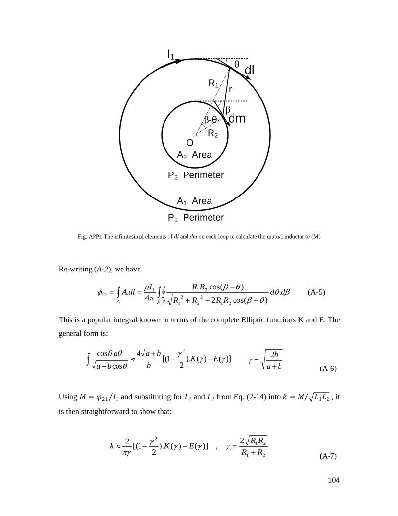
104
θ
R1
R2
r
-θ
dl
dm
A2 Area
I1
P2 Perimeter
A1 Area
P1 Perimeter
O
Fig. APP1 The infinitesimal elements of dl and dm on each loop to calculate the mutual inductance (M)
Re-writing (A-2), we have
dd
RRRR
RRIdlA
P
.)cos(2
)cos(
4.
21
2
2
2
1
21112
2
(A-5)
This is a popular integral known in terms of the complete Elliptic functions K and E. The
general form is:
)]()().2
1[(4
cos
cos 2
EK
b
ba
ba
d
ba
b
2
(A-6)
Using and substituting for L1 and L2 from Eq. (2-14) into , it
is then straightforward to show that:
21
212 2
,)]()().2
1[(2
RR
RREKk
(A-7)

105
Note that γ is only a function of R1/R2, hence one only needs to know this ratio to use this
approximation.
To derive the approximation of (2-19), note that field B1 due to current I1 is only a
function of radial distance from the center of the loop. An approximation for field B1 in
(A-1) that satisfies boundary conditions (r = 0 and r = R1) is
22
1
11
2)(
rR
IrB
(A-8)
This approximation also yields the well-known relation for the self-
inductance of the loop, where r approaches zero (r 0, R1 ≈ R2). Hence we can use
)11(
2.2
.
2
1
211
0
22
1122
1
112 |
2
22
R
RRI
rRIrdrrR
IdSB
R
AA
(A-9)
Using the mutual flux expression of (A-9) in M = 21/I1 plus the self-inductances of (2-
14) in the expression of concludes the following for the coupling factor of
the inductor:
))(11( 2
1
2
2
1
R
R
R
Rk
(A-10)
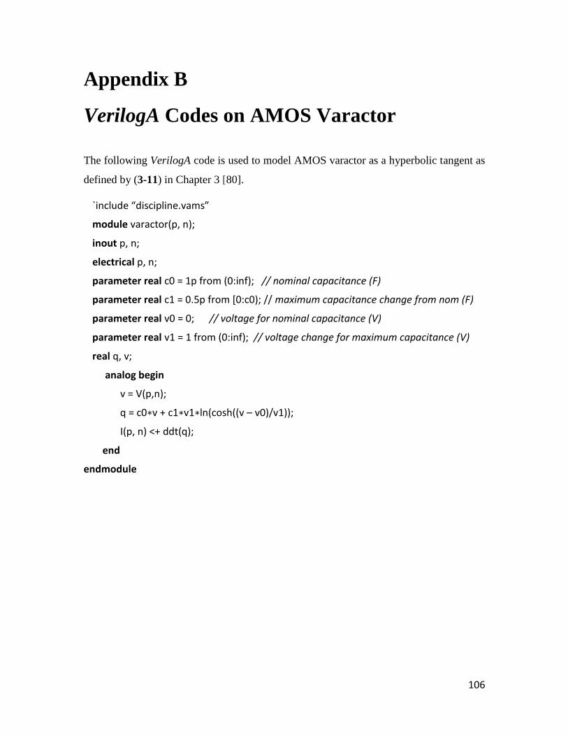
106
Appendix B
VerilogA Codes on AMOS Varactor
The following VerilogA code is used to model AMOS varactor as a hyperbolic tangent as
defined by ( 3-11) in Chapter 3 [80].
`include “discipline.vams”
module varactor(p, n);
inout p, n;
electrical p, n;
parameter real c0 = 1p from (0:inf); // nominal capacitance (F)
parameter real c1 = 0.5p from [0:c0); // maximum capacitance change from nom (F)
parameter real v0 = 0; // voltage for nominal capacitance (V)
parameter real v1 = 1 from (0:inf); // voltage change for maximum capacitance (V)
real q, v;
analog begin
v = V(p,n);
q = c0∗v + c1∗v1∗ln(cosh((v – v0)/v1));
I(p, n) <+ ddt(q);
end
endmodule
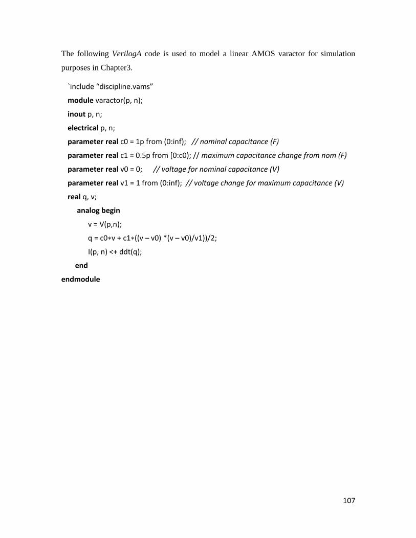
107
The following VerilogA code is used to model a linear AMOS varactor for simulation
purposes in Chapter3.
`include “discipline.vams”
module varactor(p, n);
inout p, n;
electrical p, n;
parameter real c0 = 1p from (0:inf); // nominal capacitance (F)
parameter real c1 = 0.5p from [0:c0); // maximum capacitance change from nom (F)
parameter real v0 = 0; // voltage for nominal capacitance (V)
parameter real v1 = 1 from (0:inf); // voltage change for maximum capacitance (V)
real q, v;
analog begin
v = V(p,n);
q = c0∗v + c1∗((v – v0) *(v – v0)/v1))/2;
I(p, n) <+ ddt(q);
end
endmodule
Recommended


![Small-Area CMOS RF Distributed Mixer Using Multi-Port ...masu-€¦ · Small-Area CMOS RF Distributed Mixer Using Multi-Port Inductors ... X. Fan, et al., ... conversion gain [dB]](https://img.dokumen.tips/doc/110x75/5aef60547f8b9a8b4c8c3790/small-area-cmos-rf-distributed-mixer-using-multi-port-masu-small-area-cmos.jpg)


