Design of FMCW Radar
Team Grildur Frostcrag
Charles Liu
Ghazanfar Alvi
Sandeep Banwait
Eugene Kim
Abstract
This paper presents the design and realization of a radar with the ultimate objective of providing
range measurements. The system technology implemented is classified as frequency modulation
continuous wave (FMCW) radar that can detect distances of targets and the speed of a moving
object with relatively lower power. The size of the microwave radar system can be reduced by
using higher frequencies. A 24 GHz radar design was considered but was disapproved of due to
the increase losses associated with systems operating at such high frequencies. Therefore a 5.8
GHz system has been selected for the design which also has the advantages of having readily
available components.
Introduction
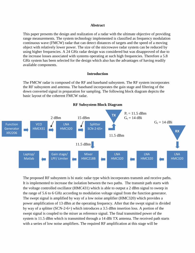
The FMCW radar is composed of the RF and baseband subsystem. The RF system incorporates
the RF subsystem and antenna. The baseband incorporates the gain stage and filtering of the
down converted signal in preparation for sampling. The following block diagram depicts the
basic layout of the coherent FMCW radar.
RF Subsystem Block Diagram
Pt = 11.5 dBm
2 dBm 15 dBm Gt = 14 dBi
Gr = 14 dBi
11.5 dBm
11.5 dBm
The proposed RF subsystem is bi static radar type which incorporates transmit and receive paths.
It is implemented to increase the isolation between the two paths. The transmit path starts with
the voltage controlled oscillator (HMC431) which is able to output a 2 dBm signal to sweep in
the range of 5.6 to 6 GHz according to modulation voltage signal from the function generator.
The swept signal is amplified by way of a low noise amplifier (HMC320) which provides a
power amplification of 13 dBm at the operating frequency. After that the swept signal is divided
by way of a splitter (SCN-2-6+) which introduces a 3.5 dBm insertion loss. A portion of the
swept signal is coupled to the mixer as reference signal. The final transmitted power of the
system is 11.5 dBm which is transmitted through a 14 dBi TX antenna. The received path starts
with a series of low noise amplifiers. The required RF amplification at this stage will be
Function Generator
XR2206
VCO HMC431
LNA HMC320
LNA HMC320
Mixer HMC218B
Splitter SCN-2-65+
LNA HMC320
LNA HMC320
TX
RX
Gain stage/ LPF/ Limiter
Laptop/ Matlab

discussed later in this section. This amplified signal from the RX antenna is inputted to the mixer
where it is down converted by mixing with the reference signal. This down converted signal is
amplified at the gain stage and passed through low pass filter before it is sampled by the PC.
Once the transmit power of the radar is realized, Frii’s equations is used to determine the
received power. The goal is to design the receiver to detect a 0.3 meter squared target ranging at
distances between 5 to 50 meters.
Pr =
With an operating frequency of 5.8 GHz the power received ranges from -52.4 dBm to -92.4
dBm for target ranges from 5 to 50 meters. To reduce the amount of amplification required at the
baseband gain stage, RF amplification is implemented at the RF receiver path with a cascade of
three low noise amplifiers (HMC320) with each providing a power amplification of 13 dBm at a
noise figure of 2.5 dBm.
To characterize the receiver path of the RF subsystem Analog Devices provides ADIsimRF to
calculated total gain, noise figure, signal to noise ratio and peak to peak output voltage. The
calculations for receiver path for targets at 5 and 50 meters are shown below.
ADIsimRF receiver path calculation for target at 5 meters
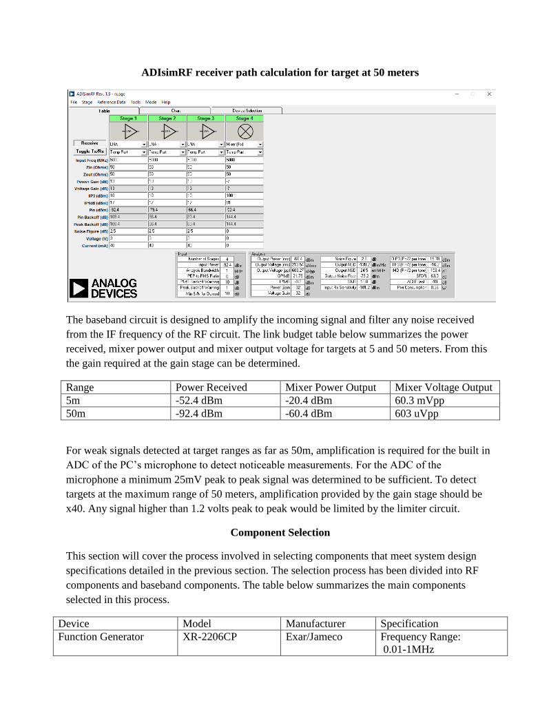
ADIsimRF receiver path calculation for target at 50 meters
The baseband circuit is designed to amplify the incoming signal and filter any noise received
from the IF frequency of the RF circuit. The link budget table below summarizes the power
received, mixer power output and mixer output voltage for targets at 5 and 50 meters. From this
the gain required at the gain stage can be determined.
Range Power Received Mixer Power Output Mixer Voltage Output
5m -52.4 dBm -20.4 dBm 60.3 mVpp
50m -92.4 dBm -60.4 dBm 603 uVpp
For weak signals detected at target ranges as far as 50m, amplification is required for the built in
ADC of the PC’s microphone to detect noticeable measurements. For the ADC of the
microphone a minimum 25mV peak to peak signal was determined to be sufficient. To detect
targets at the maximum range of 50 meters, amplification provided by the gain stage should be
x40. Any signal higher than 1.2 volts peak to peak would be limited by the limiter circuit.
Component Selection
This section will cover the process involved in selecting components that meet system design
specifications detailed in the previous section. The selection process has been divided into RF
components and baseband components. The table below summarizes the main components
selected in this process.
Device Model Manufacturer Specification
Function Generator XR-2206CP Exar/Jameco Frequency Range:
0.01-1MHz
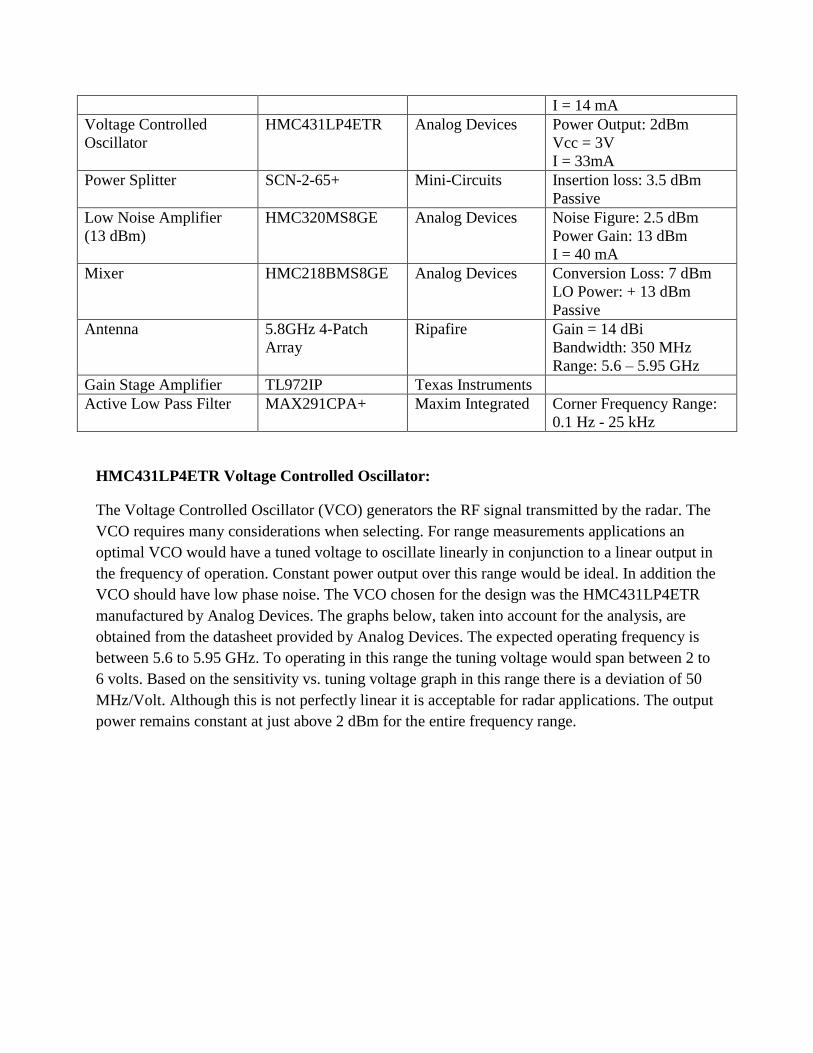
I = 14 mA
Voltage Controlled
Oscillator
HMC431LP4ETR Analog Devices Power Output: 2dBm
Vcc = 3V
I = 33mA
Power Splitter SCN-2-65+
Mini-Circuits
Insertion loss: 3.5 dBm
Passive
Low Noise Amplifier
(13 dBm)
HMC320MS8GE Analog Devices Noise Figure: 2.5 dBm
Power Gain: 13 dBm
I = 40 mA
Mixer HMC218BMS8GE Analog Devices Conversion Loss: 7 dBm
LO Power: + 13 dBm
Passive
Antenna 5.8GHz 4-Patch
Array
Ripafire Gain = 14 dBi
Bandwidth: 350 MHz
Range: 5.6 – 5.95 GHz
Gain Stage Amplifier TL972IP Texas Instruments
Active Low Pass Filter MAX291CPA+ Maxim Integrated Corner Frequency Range:
0.1 Hz - 25 kHz
HMC431LP4ETR Voltage Controlled Oscillator:
The Voltage Controlled Oscillator (VCO) generators the RF signal transmitted by the radar. The
VCO requires many considerations when selecting. For range measurements applications an
optimal VCO would have a tuned voltage to oscillate linearly in conjunction to a linear output in
the frequency of operation. Constant power output over this range would be ideal. In addition the
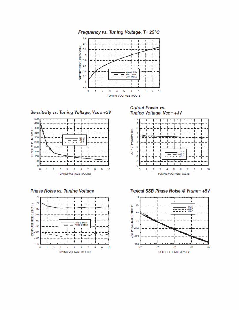
VCO should have low phase noise. The VCO chosen for the design was the HMC431LP4ETR
manufactured by Analog Devices. The graphs below, taken into account for the analysis, are
obtained from the datasheet provided by Analog Devices. The expected operating frequency is
between 5.6 to 5.95 GHz. To operating in this range the tuning voltage would span between 2 to
6 volts. Based on the sensitivity vs. tuning voltage graph in this range there is a deviation of 50
MHz/Volt. Although this is not perfectly linear it is acceptable for radar applications. The output
power remains constant at just above 2 dBm for the entire frequency range.

XR-2206CP Function Generator:
Once a VCO has been selected a function generator must be taken into account. Initially the
Teensy 3.1 in conjunction with the MCP4921 DAC was taken into consideration but due to size
and power constraints another option was chosen. The XR-2206CP is a monolithic function
generator Exar that is able to produce the required triangle waveform to drive the VCO without a
microcontroller and digital to analog converter.
HMC320MS8GE Low Noise Amplifier:
The Low Noise Amplifier (LNA) is required before the splitter and the RF input of the mixer to
allow for enough amplification of the signal entering the baseband circuit. When selecting a
LNA, it is critical to choose one that provides high power amplification and relatively low noise
figure which would reduce the signal to noise ratio introduced during cascading of multiple
LNAs. Also an LNA that does not require a complicated bias network would simplify the
assembly process. The HMC320MS8GE by Analog Devices was chosen for the radar design
which provides the option for configuration with three bias conditions. The graphs below are
obtained from the datasheet. To maximize power amplification of each LNA, a high power bias
is chosen.
SCN-2-65+ Power Splitter
When selecting a power splitter it is important to pay close attention to insertion losses and a
number of other key factors. The selection of the SCN-2-65+ Power Splitter by Mini-Circuits is
justified in the following table. For a frequency range for 5500-6500MHz the insertion loss
remains low between 3.5 and 3.8 dB. The splitter can provide a large isolation of about 17 dB
which is good. Also the splitter had the added benefit of easy soldering and being low on cost.
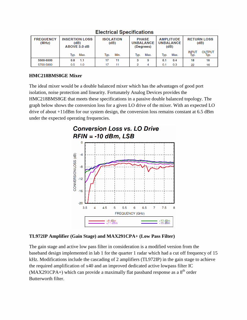
HMC218BMS8GE Mixer
The ideal mixer would be a double balanced mixer which has the advantages of good port
isolation, noise protection and linearity. Fortunately Analog Devices provides the
HMC218BMS8GE that meets these specifications in a passive double balanced topology. The
graph below shows the conversion loss for a given LO drive of the mixer. With an expected LO
drive of about +11dBm for our system design, the conversion loss remains constant at 6.5 dBm
under the expected operating frequencies.
TL972IP Amplifier (Gain Stage) and MAX291CPA+ (Low Pass Filter)
The gain stage and active low pass filter in consideration is a modified version from the
baseband design implemented in lab 1 for the quarter 1 radar which had a cut off frequency of 15
kHz. Modifications include the cascading of 2 amplifiers (TL972IP) in the gain stage to achieve
the required amplification of x40 and an improved dedicated active lowpass filter IC
(MAX291CPA+) which can provide a maximally flat passband response as a 8th
order
Butterworth filter.
Design Schematics and Printed Circuit Board Designs
A Printed Circuit Board (PCB) is a board made up of a set of pads and copper interconnects that
connect at various points to create a proper circuit. PCBs are made up of a substrate (usually
fiberglass), copper wirings, soldermask, and silkscreens all stacked up in layers to achieve a
compact design. The use of PCB simplifies the wiring process, reduces error caused by wiring,
and decreases the overall size and weight of the device. The absence of messy wires gives us
cleaner runs and user-placed test pins allow for fasts and easy debugging. For our project, we
used KiCAD to design the schematics and PCB layouts of our PCBs. KiCAD is not only free,
but straightforward in the way that it simplifies the conversion from schematic to PCB layout
design. Another option would be to use EAGLE, but the fact that its free version is not for
commercial use makes it less appealing to KiCAD.
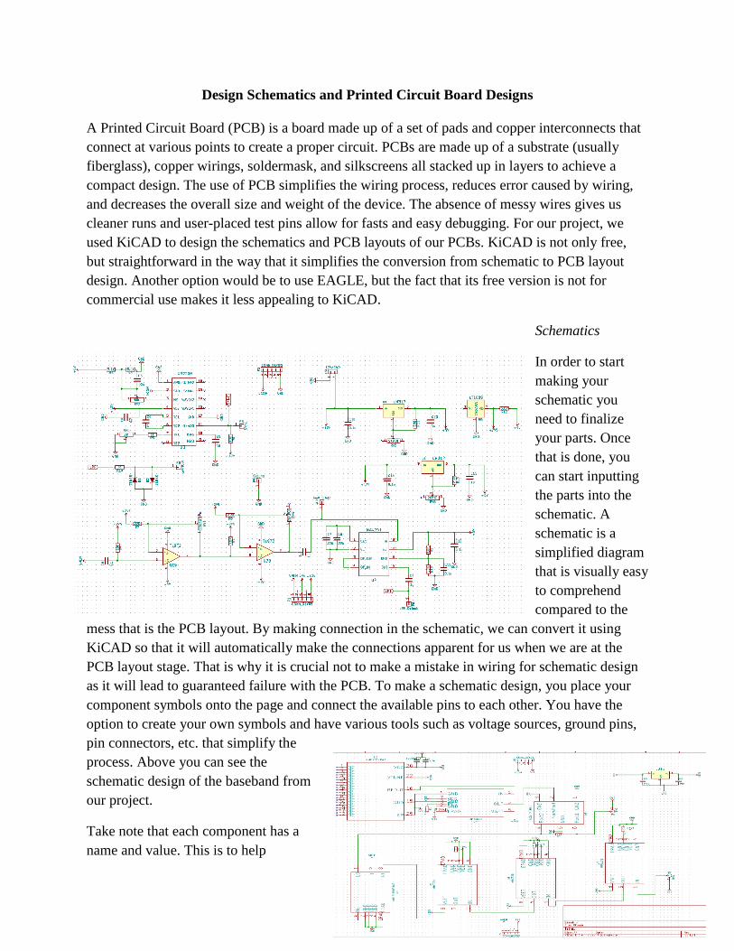
Schematics
In order to start
making your
schematic you
need to finalize
your parts. Once
that is done, you
can start inputting
the parts into the
schematic. A
schematic is a
simplified diagram
that is visually easy
to comprehend
compared to the
mess that is the PCB layout. By making connection in the schematic, we can convert it using
KiCAD so that it will automatically make the connections apparent for us when we are at the
PCB layout stage. That is why it is crucial not to make a mistake in wiring for schematic design
as it will lead to guaranteed failure with the PCB. To make a schematic design, you place your
component symbols onto the page and connect the available pins to each other. You have the
option to create your own symbols and have various tools such as voltage sources, ground pins,
pin connectors, etc. that simplify the
process. Above you can see the
schematic design of the baseband from
our project.
Take note that each component has a
name and value. This is to help
differentiate the components once they are placed on the board. For our circuit U2A and U2B are
the same component, but if they were two different, yet similar components then the part’s label
would be very important to avoid mismatching. On the right is the RF schematic for our radar.
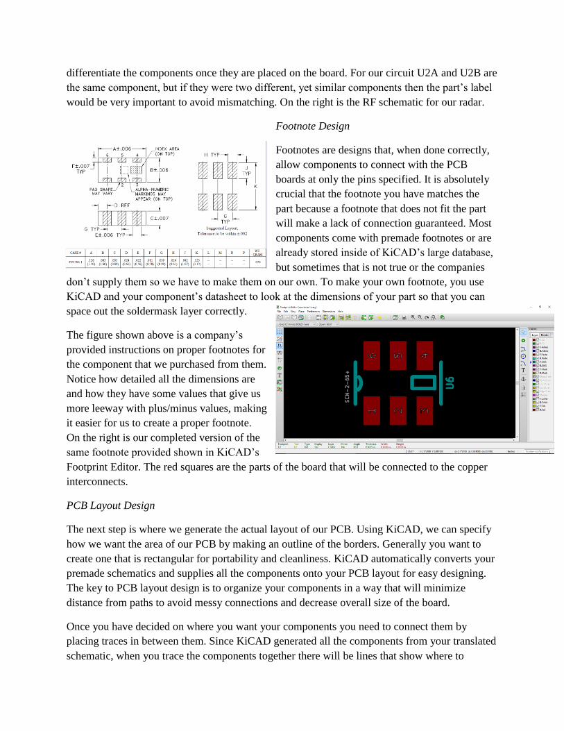
Footnote Design
Footnotes are designs that, when done correctly,
allow components to connect with the PCB
boards at only the pins specified. It is absolutely
crucial that the footnote you have matches the
part because a footnote that does not fit the part
will make a lack of connection guaranteed. Most
components come with premade footnotes or are
already stored inside of KiCAD’s large database,
but sometimes that is not true or the companies
don’t supply them so we have to make them on our own. To make your own footnote, you use
KiCAD and your component’s datasheet to look at the dimensions of your part so that you can
space out the soldermask layer correctly.
The figure shown above is a company’s
provided instructions on proper footnotes for
the component that we purchased from them.
Notice how detailed all the dimensions are
and how they have some values that give us
more leeway with plus/minus values, making
it easier for us to create a proper footnote.
On the right is our completed version of the
same footnote provided shown in KiCAD’s
Footprint Editor. The red squares are the parts of the board that will be connected to the copper
interconnects.
PCB Layout Design
The next step is where we generate the actual layout of our PCB. Using KiCAD, we can specify
how we want the area of our PCB by making an outline of the borders. Generally you want to
create one that is rectangular for portability and cleanliness. KiCAD automatically converts your
premade schematics and supplies all the components onto your PCB layout for easy designing.
The key to PCB layout design is to organize your components in a way that will minimize
distance from paths to avoid messy connections and decrease overall size of the board.
Once you have decided on where you want your components you need to connect them by
placing traces in between them. Since KiCAD generated all the components from your translated
schematic, when you trace the components together there will be lines that show where to
connect each part. This is really convenient because without this tool you would need to
manually check with the schematic to make sure of where you should be connecting and that
would take too much time. You can place a trace on either the front or back copper layer and
connect them together by using a via. This simplifies the process when there are too many
connections already on one side giving us more space to connect. It is ideal to only use one layer,
but it is not realistic for circuits that have many components especially when trying to decrease
board size. Make sure not to place the vias directly on the pins of the components, this will cause
improper connections. Another thing to point out is to be cautious of trace length and width. The
longer the length the greater the dissipation of power so we aim for shorter length to give more
power to the circuit. Same goes for width where we want thicker traces, however this is harder to
do when trying to minimize board area since larger trace width means less space to connect with.
Another important note is that trace connections should avoid making sharp ninety degree turns.
These result in issues due to manufacturers not being able to etch it properly.
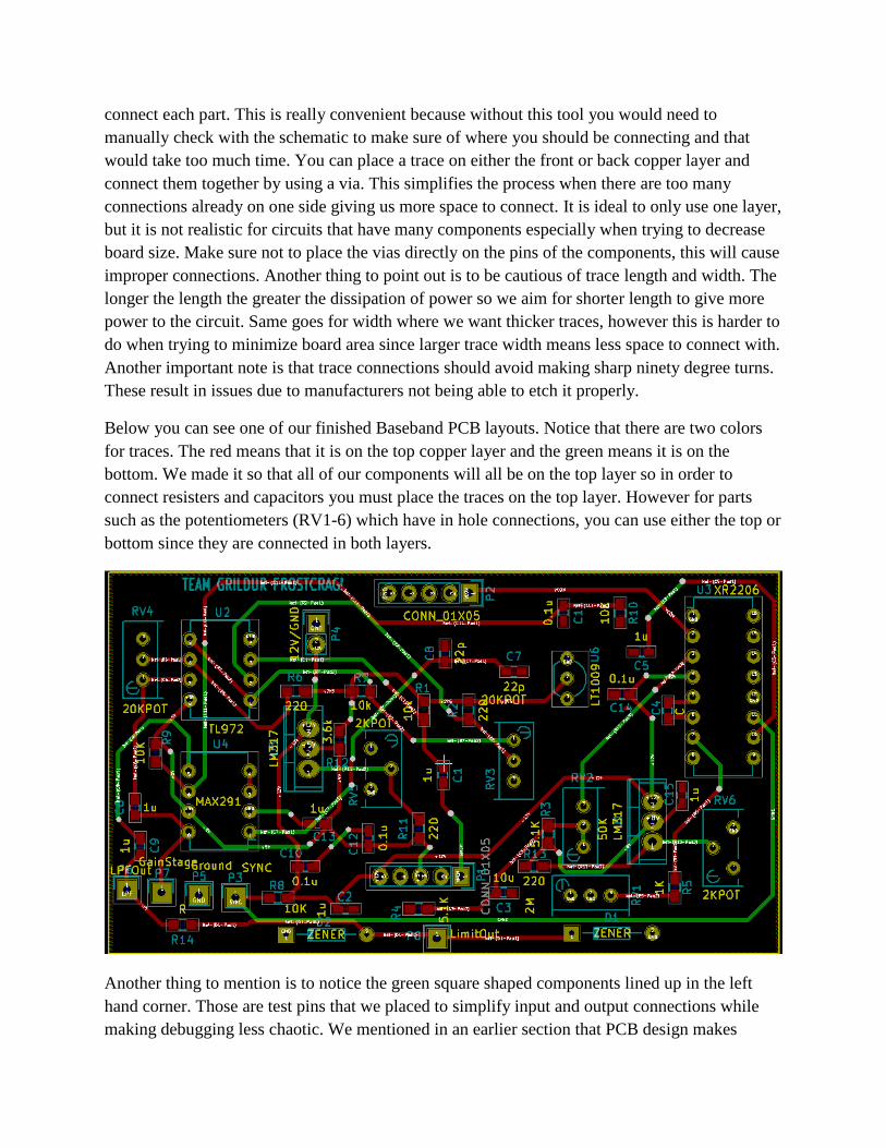
Below you can see one of our finished Baseband PCB layouts. Notice that there are two colors
for traces. The red means that it is on the top copper layer and the green means it is on the
bottom. We made it so that all of our components will all be on the top layer so in order to
connect resisters and capacitors you must place the traces on the top layer. However for parts
such as the potentiometers (RV1-6) which have in hole connections, you can use either the top or
bottom since they are connected in both layers.
Another thing to mention is to notice the green square shaped components lined up in the left
hand corner. Those are test pins that we placed to simplify input and output connections while
making debugging less chaotic. We mentioned in an earlier section that PCB design makes
debugging easier and it is the capabilities that test pins give us that allow for clean and simple
debugging of our circuit.
RF PCB Layout
Because of the high frequencies used for RF circuits we must take note of the traces. The
transmission lines must not be perpendicular to each other and should remain as straight as
possible because turns can cause a 180 degree phase dissonance causing the signal to weaken or
cancel. Notice that there are two paths so they may look like they are going ninety degrees but
they are separate paths.
In the figure on the left is one of our finished
RF PCB layouts. As you can see there are
numerous amount of vias scattered around the
PCB. The vias are necessary around the
transmission line in order to prevent RF signals
from resonating onto the ground plane and
stops the generation of noise. Using a web app
called Wcalc we were able to find the
parameters needed to make accurate
transmission line width and spacing. As shown
in the picture below, by inputting our fixed 6.15
mil spacing parameter we were able to get our
transmission line width which isis 37.5 mil.
Printed Circuit Board Assemblies

Soldering, using fusible metal alloy as an adhesive, played a key role in constructing the quarter
two RF radars. It is imperative that soldering is done correctly, otherwise, one erroneous
connection can make the difference between a working and non-working system, potentially
causing time consuming troubleshooting and frustration. The components previously prototyped
on a bread board in quarter one, are now compacted into different shaped integrated circuits and
passive components that lie in the realms of millimeters; with each different shaped component,
there are several techniques and tools that can ensure a proper connection.
Safety Concerns
Before soldering, it is HIGHLY recommended to put on googles. While soldering, bits of solder
may fly out and if you’re looking closely at the board, which tends to happen while soldering the
smaller passive components, melted bits of solder, upon contact, can cause permanent damage to
the eyes. Also, there may be cases where a peer may accidentally bump into you, causing the
solder tip to jerk towards you’re face. Although these cases may seem very situational, you may
prevent these permanent consequences with simple eyewear.
The soldering iron is typically 600 to 750 degrees fahrenheit, so please be aware of where you
each whenever you grab the iron as well as your surroundings. Quickly turning while holding the
iron, may come into brief contact with a peer who the user isn't aware of, however this brief
contact is more than enough to cause serious burns. Also when soldering a wire you may find it
quickly heats up, so it is advised to hold the writes with tweezers or clamps to avoid burns.
It is also advised to work with constant ventilation: near a window, or have a fan running that
may direct the solder fumes away from the solderer. The most common types of solder is a lead-
tin alloy with a rosin core, which cause fumes that is known to cause occupational asthma and
dermatitis. If ventilation isn't possible, you may want to consider investing in a face mask.
Finally, as mentioned above, the most common type of solder is has strong concentration of lead
which is a known neurotoxin. Lead can pose significant chronic health effects with digestive
problems, memory, and reproductive problems [1]. Although lead is harmless upon direct skin
contact, problems arise when dust from lead remains on the solderer’s hands which can be
ingested when eating, smoking, biting nails, etc, so it is highly suggested to wash your hands
after each soldering session.
Different methods
There are three main methods that were utilized for constructing our radar: Hot Iron, Hot plate,
and Hot Air. Hot Iron is analogous to a heated pen, which can melt solder at precise locations,
and clean up existing connections. Hot plate uses, as the name implies, a hot plate where a
printed circuit board (PCB) may sit on top on, and conduct enough heat to melt solder on the
surface. Finally, Hot air is essentially a blow dryer, that typically operates in the range of 275 -
400 degrees Fahrenheit
ahrenheit, and is primarily for specific connections and aligning existing connections. Figure 1. Hot Iron, Hot Plate, Hot Air.
Hot Iron
Hot iron was the primary method in constructing our PCBs. Because the Hot Iron is only heating
a specific part of the PCB and the Iron can be simply lifted off the PCB if damage is a concern, I
found it to be the safest method of construction. Hot Iron works well with smaller components
such as resistors and capacitors, but it cannot be used for IC components that have a grounded
pad. If there are different tips available, typical the more finer the tip, you will have better
accuracy and control of applied the solder. Before soldering, I would clean the iron of any excess
solder by heating it up, and scraping it with steel wool. Also if the iron looks dull, I would apply
some solder onto the tip, and clean it until it looks shiny. If the iron looks dull, it may transfer
heat slower, so cleaning it after each use is advised.
To begin, I will go over soldering potentiometers, pin headers, and other pin based PCB
components. Before soldering, have the components in place into the PCB positioned as you
intend them to stay in. Have the hot iron in your dominant hand, and the solder wire in the other.
Soldering from the bottom side of the vi, first place the soldering iron onto the vi, and then apply
solder to the tip of the iron, where it’s in contact with the vi. After applying solder, remove the
iron first, and keep the component in place for a second or so to let the solder harden. Once one
pin is in place, it is unlikely that the rest will move from place, so you may quickly solder the
other pins without being concerned with holding the rest of the pins in place.
Moving on, I will discuss how to solder resistors and capacitors. Put the tip of the iron in contact
with the copper pad, then quickly dab the solder wire at the tip. Due to the nature of the solder, it
will reposition itself on the copper, so you do not need to be concerned with solder positioned
outside the footprint. Once you have successfully applied solder onto one side of a interconnect,
grab your passive components with a sharp tipped tweezers. Make sure to level you passive
component as flat as possible with the PCB to ensure a strong connection and to prevent
tombing. Once you have leveled your passive component, heat the solder previously applied,
then slide the passive component into place. Remove the iron first then the tweezers. Hold the
component in place with tweezers, and after a second or so, the solder should be hardened and
the component should be in place. To finish the connection, apply solder onto the other side of
the component.
*Note, you do not need a large amount of solder for a sufficient connection; very little solder is
needed for a proper connection. An indication of an appropriate amount of solder is to look for a
“heel” shape connection, but for those who are unsure, a small ball of solder connection is more
than enough. The capacitor on the left has two small balls of solder for its connection while the
resistor, the left side in particular, has a “heel” shape connection.
Hot Plate
As shown in figure 1, the hot plate is a very simple device. Simply set the setting of by turning
the knob, and the light shown on the front-left side of the device indicates whether or not the
plate is active. The hot plate works well with soldering IC components, especially ones with a
grounded connection underneath the component pad. With the hot plate, you will be using solder
flux which is a gray paste in a syringe that has a lower melting point than traditional solder. Be
warned, if the PCB is left on the plate for too long, it can easily damage the board, so you must
Figure 2. Different types of proper connections.
work quickly once it’s in use.
To begin, apply a small amount of paste onto the all the connection sites you intend to use the
hot plate for. It is better to set all your IC’s in as few runs as possible because with each run,
there is a higher risk of damaging the PCB with every trial. Set the hot plate onto low, or around
230F, and place the PCB onto the pad. The paste will quickly melt and look just like traditionally
melted solder. Once the paste as melted, quickly place your components on top of the melted
solder. To know if there is a good connection, tap the components to the side very lightly and the
solder should snap the IC back into place. Once all the components are placed properly, carefully
move the PCB off the plate. From my experience, solder paste solidifies much slower than rosen
core solder, so be wary of components moved from place, and solidifying improperly. Also, do
not try to move a hot plated pcb with your bare hands; it will be extremely hot. Also we wary
with the amount of solder paste applied: if to much solder is applied, IC legs may become
shorted with one another and establish connections that lead to failure.
Hot Air
Shown in figure, the hot air is also another simple device. Once lifted off it’s stand, it will begin
heating up, and once its placed back into the stand, it will automatically shut itself off. I
typically operated the hot air at 270C, which is hot enough to melt both types of solders. Hot Air
is a great tool to realign solder components, and could also be a tool to form connections as well.
Before applying hot air onto the solder, I always make sure to apply drops of flux where i’m
going to air to help with the conduction and to remove impurities at the solder connection site.
Also, if you make solder connections on all the connection sites of your component, for an
example both sides of a resistor, then you can rely on hot air to properly align them. In figure 4,
the PCB is shown before applying hot air, and is evidently unpolished. However if there is solder
at each connection footprint, the hot air will snap each component into place. This greatly speeds
Figure 3.
up the soldering process because if there is a sufficient connection, you can simply hot air it later
to refine it, instead of attempting to perfectly align every component when its initially
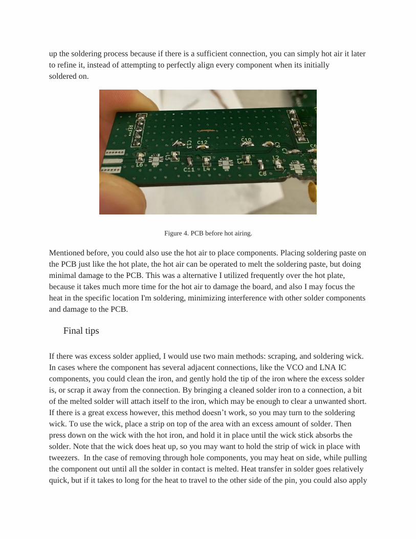
soldered on.
Figure 4. PCB before hot airing.
Mentioned before, you could also use the hot air to place components. Placing soldering paste on
the PCB just like the hot plate, the hot air can be operated to melt the soldering paste, but doing
minimal damage to the PCB. This was a alternative I utilized frequently over the hot plate,
because it takes much more time for the hot air to damage the board, and also I may focus the
heat in the specific location I'm soldering, minimizing interference with other solder components
and damage to the PCB.
Final tips
If there was excess solder applied, I would use two main methods: scraping, and soldering wick.
In cases where the component has several adjacent connections, like the VCO and LNA IC
components, you could clean the iron, and gently hold the tip of the iron where the excess solder
is, or scrap it away from the connection. By bringing a cleaned solder iron to a connection, a bit
of the melted solder will attach itself to the iron, which may be enough to clear a unwanted short.
If there is a great excess however, this method doesn’t work, so you may turn to the soldering
wick. To use the wick, place a strip on top of the area with an excess amount of solder. Then
press down on the wick with the hot iron, and hold it in place until the wick stick absorbs the
solder. Note that the wick does heat up, so you may want to hold the strip of wick in place with
tweezers. In the case of removing through hole components, you may heat on side, while pulling
the component out until all the solder in contact is melted. Heat transfer in solder goes relatively
quick, but if it takes to long for the heat to travel to the other side of the pin, you could also apply
two soldering irons on each side, while a second person pulls on the component until it frees.
Once you remove a pinhole component, there are times where excess solder remains in the vi,
which may block any future components going in. To remove this solder, you could use the
wick, or another tool called the soldering tube. It acts as a vacuum, and sucks in any melted
solder. First you would heat one side of the vi, and then place the opening of the tube as flat as
possible on the other. Once the solder melts, you release the spring in tube, the black button in
figure 5, and it will suck the solder up.
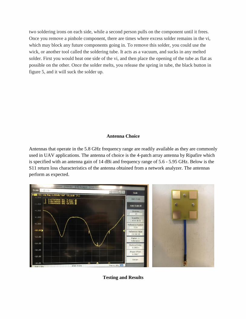
Antenna Choice
Antennas that operate in the 5.8 GHz frequency range are readily available as they are commonly
used in UAV applications. The antenna of choice is the 4-patch array antenna by Ripafire which
is specified with an antenna gain of 14 dBi and frequency range of 5.6 - 5.95 GHz. Below is the
S11 return loss characteristics of the antenna obtained from a network analyzer. The antennas
perform as expected.
Testing and Results
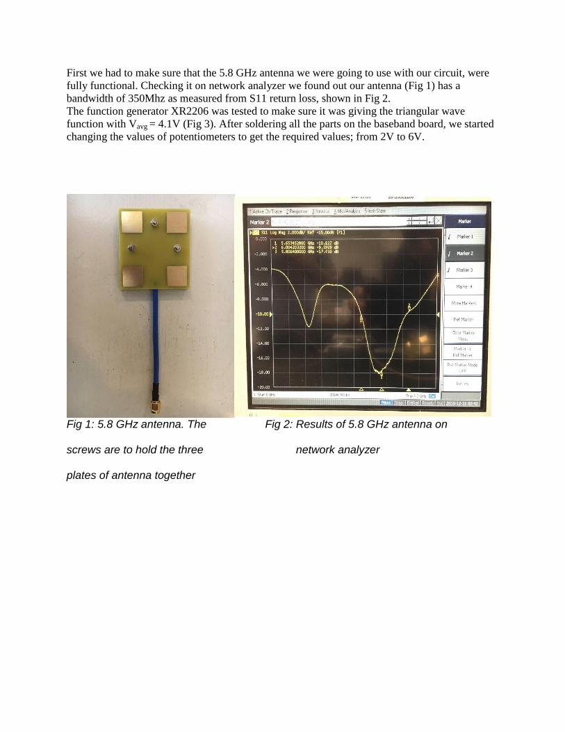
First we had to make sure that the 5.8 GHz antenna we were going to use with our circuit, were
fully functional. Checking it on network analyzer we found out our antenna (Fig 1) has a
bandwidth of 350Mhz as measured from S11 return loss, shown in Fig 2.
The function generator XR2206 was tested to make sure it was giving the triangular wave
function with Vavg = 4.1V (Fig 3). After soldering all the parts on the baseband board, we started
changing the values of potentiometers to get the required values; from 2V to 6V.
Fig 1: 5.8 GHz antenna. The Fig 2: Results of 5.8 GHz antenna on
screws are to hold the three network analyzer
plates of antenna together
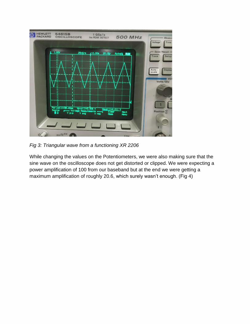
Fig 3: Triangular wave from a functioning XR 2206
While changing the values on the Potentiometers, we were also making sure that the
sine wave on the oscilloscope does not get distorted or clipped. We were expecting a
power amplification of 100 from our baseband but at the end we were getting a
maximum amplification of roughly 20.6, which surely wasn’t enough. (Fig 4)
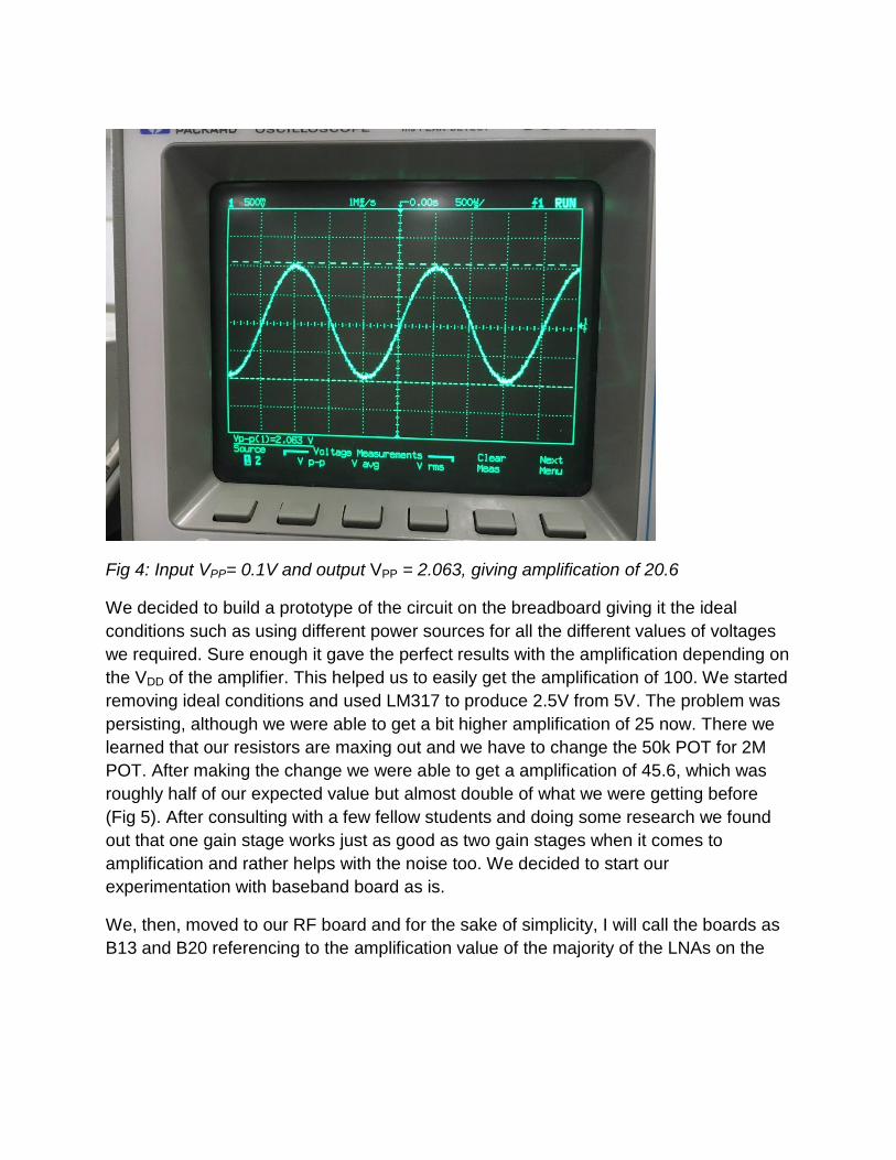
Fig 4: Input VPP= 0.1V and output VPP = 2.063, giving amplification of 20.6
We decided to build a prototype of the circuit on the breadboard giving it the ideal
conditions such as using different power sources for all the different values of voltages
we required. Sure enough it gave the perfect results with the amplification depending on
the VDD of the amplifier. This helped us to easily get the amplification of 100. We started
removing ideal conditions and used LM317 to produce 2.5V from 5V. The problem was
persisting, although we were able to get a bit higher amplification of 25 now. There we
learned that our resistors are maxing out and we have to change the 50k POT for 2M
POT. After making the change we were able to get a amplification of 45.6, which was
roughly half of our expected value but almost double of what we were getting before
(Fig 5). After consulting with a few fellow students and doing some research we found
out that one gain stage works just as good as two gain stages when it comes to
amplification and rather helps with the noise too. We decided to start our
experimentation with baseband board as is.
We, then, moved to our RF board and for the sake of simplicity, I will call the boards as
B13 and B20 referencing to the amplification value of the majority of the LNAs on the
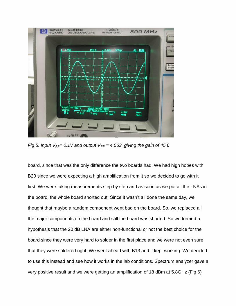
Fig 5: Input VPP= 0.1V and output VPP = 4.563, giving the gain of 45.6
board, since that was the only difference the two boards had. We had high hopes with
B20 since we were expecting a high amplification from it so we decided to go with it
first. We were taking measurements step by step and as soon as we put all the LNAs in
the board, the whole board shorted out. Since it wasn’t all done the same day, we
thought that maybe a random component went bad on the board. So, we replaced all
the major components on the board and still the board was shorted. So we formed a
hypothesis that the 20 dB LNA are either non-functional or not the best choice for the
board since they were very hard to solder in the first place and we were not even sure
that they were soldered right. We went ahead with B13 and it kept working. We decided
to use this instead and see how it works in the lab conditions. Spectrum analyzer gave a
very positive result and we were getting an amplification of 18 dBm at 5.8GHz (Fig 6)
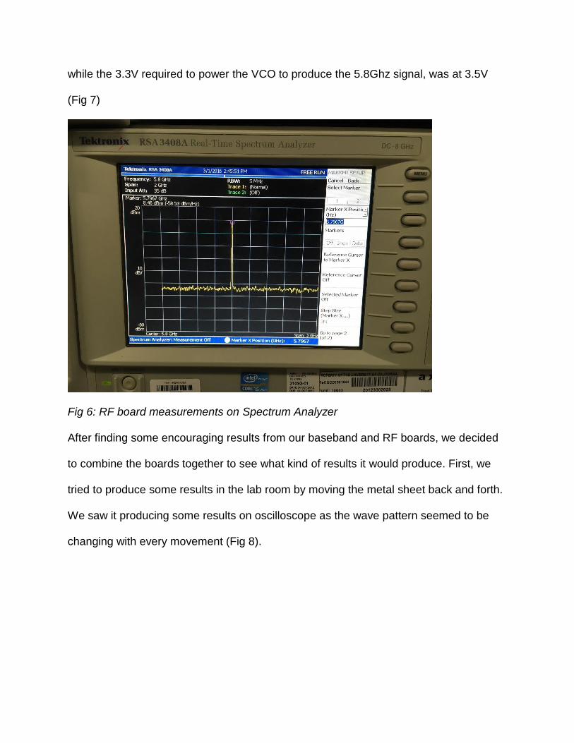
while the 3.3V required to power the VCO to produce the 5.8Ghz signal, was at 3.5V
(Fig 7)
Fig 6: RF board measurements on Spectrum Analyzer
After finding some encouraging results from our baseband and RF boards, we decided
to combine the boards together to see what kind of results it would produce. First, we
tried to produce some results in the lab room by moving the metal sheet back and forth.
We saw it producing some results on oscilloscope as the wave pattern seemed to be
changing with every movement (Fig 8).
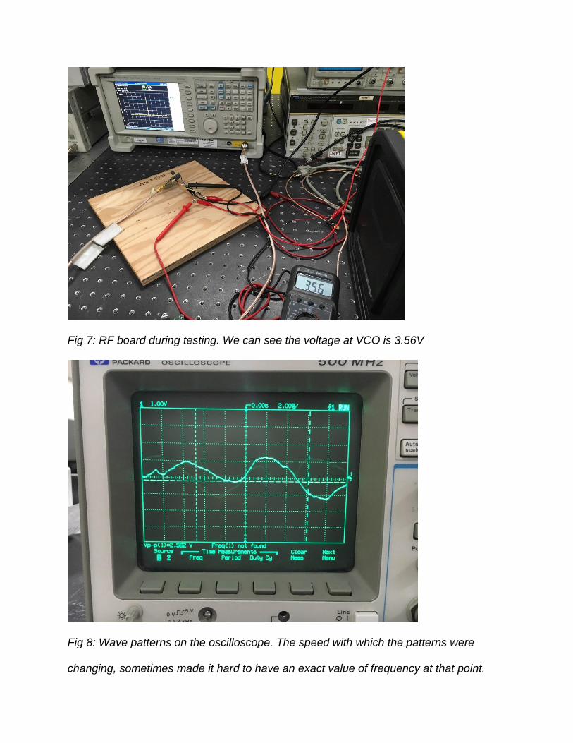
Fig 7: RF board during testing. We can see the voltage at VCO is 3.56V
Fig 8: Wave patterns on the oscilloscope. The speed with which the patterns were
changing, sometimes made it hard to have an exact value of frequency at that point.
5.8 GHz Patch Antenna Radar
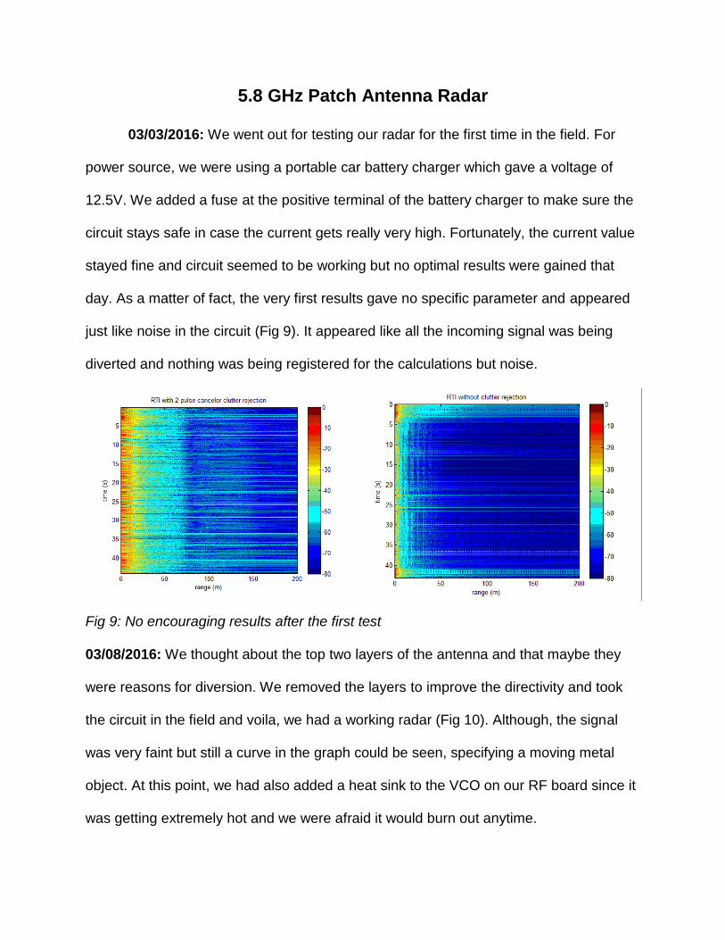
03/03/2016: We went out for testing our radar for the first time in the field. For
power source, we were using a portable car battery charger which gave a voltage of
12.5V. We added a fuse at the positive terminal of the battery charger to make sure the
circuit stays safe in case the current gets really very high. Fortunately, the current value
stayed fine and circuit seemed to be working but no optimal results were gained that
day. As a matter of fact, the very first results gave no specific parameter and appeared
just like noise in the circuit (Fig 9). It appeared like all the incoming signal was being
diverted and nothing was being registered for the calculations but noise.
Fig 9: No encouraging results after the first test
03/08/2016: We thought about the top two layers of the antenna and that maybe they
were reasons for diversion. We removed the layers to improve the directivity and took
the circuit in the field and voila, we had a working radar (Fig 10). Although, the signal
was very faint but still a curve in the graph could be seen, specifying a moving metal
object. At this point, we had also added a heat sink to the VCO on our RF board since it
was getting extremely hot and we were afraid it would burn out anytime.
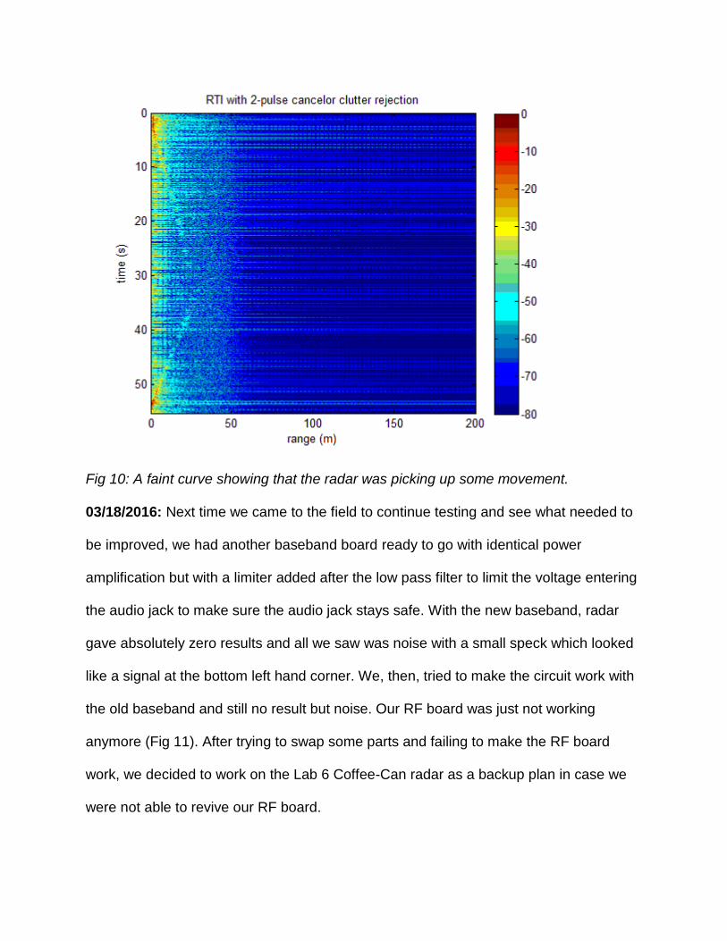
Fig 10: A faint curve showing that the radar was picking up some movement.
03/18/2016: Next time we came to the field to continue testing and see what needed to
be improved, we had another baseband board ready to go with identical power
amplification but with a limiter added after the low pass filter to limit the voltage entering
the audio jack to make sure the audio jack stays safe. With the new baseband, radar
gave absolutely zero results and all we saw was noise with a small speck which looked
like a signal at the bottom left hand corner. We, then, tried to make the circuit work with
the old baseband and still no result but noise. Our RF board was just not working
anymore (Fig 11). After trying to swap some parts and failing to make the RF board
work, we decided to work on the Lab 6 Coffee-Can radar as a backup plan in case we
were not able to revive our RF board.
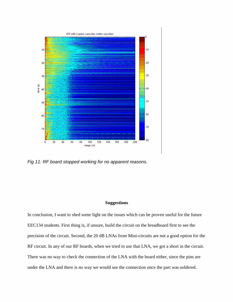
Fig 11: RF board stopped working for no apparent reasons.
Suggestions
In conclusion, I want to shed some light on the issues which can be proven useful for the future
EEC134 students. First thing is, if unsure, build the circuit on the breadboard first to see the
precision of the circuit. Second, the 20 dB LNAs from Mini-circuits are not a good option for the
RF circuit. In any of our RF boards, when we tried to use that LNA, we got a short in the circuit.
There was no way to check the connection of the LNA with the board either, since the pins are
under the LNA and there is no way we would see the connection once the part was soldered.

Thirdly, even if you are told something is not available in the market, don’t give up and try to
find it anyways or may be try for an after-market alternative. We were told the XR2206 function
generator was not available in the market. We did a little bit of research and in the end we were
able to find an after-market version from china which worked just as great and saved us all the
headache of working with Teensy and trying to produce the same exact results which we
produced with a smaller component and a potentiometer. Fourth, RF results are lot better during
a sunny day compared to a cloudy day and even worse for night. So, plan to do your testing on a
good sunny day. Fifth, as I mentioned before, one gain stage for the baseband will work just as
great as two gain stages and with lot less noise. You can always try to build it on the breadboard
first if you want to test the accuracy of my statement. Sixth, for the limiter, it is best to use Zener
diodes (consult Professor Momeni for more information on how these work to make a limiter).
Seventh, do not but do not make 90 degree angles on transmission lines, since it will bring up the
issue with return ratio and return loss. Lastly, always have a lot of test points, especially on the
baseband board and especially after the gain stages, LPF, sync signal and limiter signal. It always
helps you to find the problem at the most important parts of the circuit and helps you to take care
of those problems without affecting any other part of circuit in any way.
Conclusion
This project covered the entire engineering process involved in designing and implementing a
RF system from start to finish. We started out by researching design specifications used to meet
the specific performance requirements. Once these system characteristics were well defined, the
implementation process of component selection was undertaken. This led to the design of
schematic CAD drawings and printed circuit board layouts which were sent out for fabrication.
The purchasing process was taken care of to insure the parts arrived when the PCBs were
received from fabrication. Next the PCB assembly process required extensively precise soldering
work to insure proper connection of components without any shorts. We finished with fine
tuning, modifying and field testing of the complete radar.

Overall the radar performed reasonably well. During the testing phase of the project, our radar
was able detect a 0.3 meter squared metal target at distances of 25 meters in the field. More time
spent on fine tuning distance measurements would have greatly helpful in reducing noise and
distortion in our readings to achieving the 50 meter range mark. In conclusion this project
provides the engineering skills required to take on and overcome the challenges presented in RF
system design.
Appendix
MatLab Code: %MIT IAP Radar Course 2011 %Resource: Build a Small Radar System Capable of Sensing Range, Doppler, %and Synthetic Aperture Radar Imaging % %Gregory L. Charvat
%Process Range vs. Time Intensity (RTI) plot
%NOTE: set up-ramp sweep from 2-3.2V to stay within ISM band %change fstart and fstop bellow when in ISM band
clear all; close all;
%read the raw data .wave file here [Y,FS,NBITS] = wavread('running_outside_20ms.wav');
%constants c = 3E8; %(m/s) speed of light
%radar parameters Tp = 20E-3; %(s) pulse time N = Tp*FS; %# of samples per pulse fstart = 2260E6; %(Hz) LFM start frequency for example fstop = 2590E6; %(Hz) LFM stop frequency for example %fstart = 2402E6; %(Hz) LFM start frequency for ISM band %fstop = 2495E6; %(Hz) LFM stop frequency for ISM band BW = fstop-fstart; %(Hz) transmti bandwidth f = linspace(fstart, fstop, N/2); %instantaneous transmit frequency
%range resolution rr = c/(2*BW); max_range = rr*N/2;
%the input appears to be inverted trig = -1*Y(:,1); s = -1*Y(:,2); clear Y;
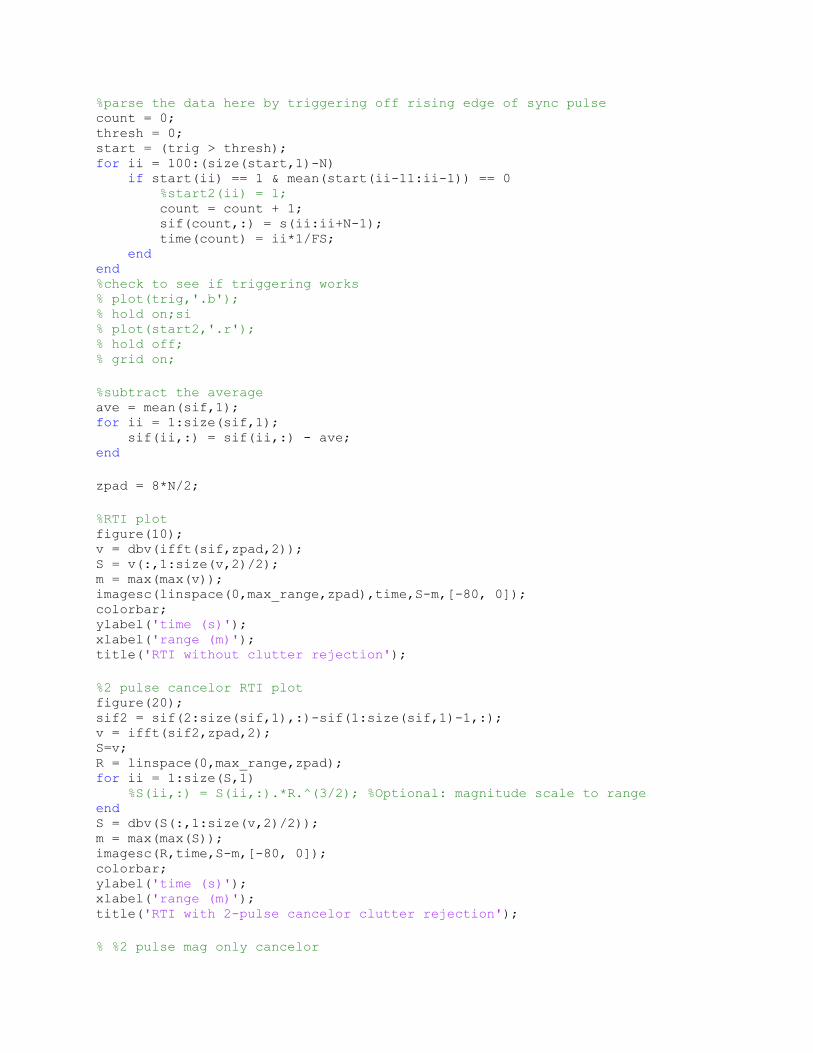
%parse the data here by triggering off rising edge of sync pulse count = 0; thresh = 0; start = (trig > thresh); for ii = 100:(size(start,1)-N) if start(ii) == 1 & mean(start(ii-11:ii-1)) == 0 %start2(ii) = 1; count = count + 1; sif(count,:) = s(ii:ii+N-1); time(count) = ii*1/FS; end end %check to see if triggering works % plot(trig,'.b'); % hold on;si % plot(start2,'.r'); % hold off; % grid on;
%subtract the average ave = mean(sif,1); for ii = 1:size(sif,1); sif(ii,:) = sif(ii,:) - ave; end
zpad = 8*N/2;
%RTI plot figure(10); v = dbv(ifft(sif,zpad,2)); S = v(:,1:size(v,2)/2); m = max(max(v)); imagesc(linspace(0,max_range,zpad),time,S-m,[-80, 0]); colorbar; ylabel('time (s)'); xlabel('range (m)'); title('RTI without clutter rejection');
%2 pulse cancelor RTI plot figure(20); sif2 = sif(2:size(sif,1),:)-sif(1:size(sif,1)-1,:); v = ifft(sif2,zpad,2); S=v; R = linspace(0,max_range,zpad); for ii = 1:size(S,1) %S(ii,:) = S(ii,:).*R.^(3/2); %Optional: magnitude scale to range end S = dbv(S(:,1:size(v,2)/2)); m = max(max(S)); imagesc(R,time,S-m,[-80, 0]); colorbar; ylabel('time (s)'); xlabel('range (m)'); title('RTI with 2-pulse cancelor clutter rejection');
% %2 pulse mag only cancelor
% figure(30); % clear v; % for ii = 1:size(sif,1)-1 % v1 = abs(ifft(sif(ii,:),zpad)); % v2 = abs(ifft(sif(ii+1,:),zpad)); % v(ii,:) = v2-v1; % end % S=v; % R = linspace(0,max_range,zpad); % for ii = 1:size(S,1) % S(ii,:) = S(ii,:).*R.^(3/2); %Optional: magnitude scale to range % end % S = dbv(S(:,1:size(v,2)/2)); % m = max(max(S)); % imagesc(R,time,S-m,[-20, 0]); % colorbar; % ylabel('time (s)'); % xlabel('range (m)'); % title('RTI with 2-pulse mag only cancelor clutter rejection');
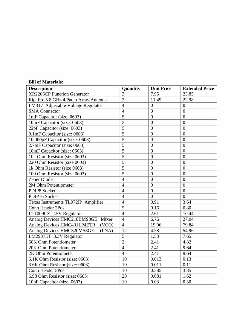
Bill of Materials:
Description Quantity Unit Price Extended Price
XR2206CP Function Generator 3 7.95 23.85
Ripafire 5.8 GHz 4 Patch Array Antenna 2 11.49 22.98
LM317 Adjustable Voltage Regulator 4 0 0
SMA Connector 4 0 0
1mF Capacitor (size: 0603) 5 0 0
10mF Capacitor (size: 0603) 5 0 0
22pF Capacitor (size: 0603) 5 0 0
0.1mF Capacitor (size: 0603) 5 0 0
10,000pF Capacitor (size: 0603) 5 0 0
2.7mF Capacitor (size: 0603) 5 0 0
10mF Capacitor (size: 0603) 5 0 0
10k Ohm Resistor (size 0603) 5 0 0
220 Ohm Resistor (size 0603) 5 0 0
1k Ohm Resistor (size 0603) 5 0 0
100 Ohm Resistor (size 0603) 5 0 0
Zener Diode 4 0 0
2M Ohm Potentiometer 4 0 0
PDIP8 Socket 4 0 0
PDIP16 Socket 4 0 0
Texas Instruments TL972IP Amplifier 4 0.91 3.64
Conn Header 2Pos 5 0.16 0.80
LT1009CZ 2.5V Regulator 4 2.61 10.44
Analog Devices HMC218BMS8GE Mixer 4 6.76 27.04
Analog Devices HMC431LP4ETR (VCO) 4 19.96 79.84
Analog Devices HMC320MS8GE (LNA) 12 4.58 54.96
LM2937ET 3.3V Regulator 5 1.53 7.65
50K Ohm Potentiometer 2 2.41 4.82
20K Ohm Potentiometer 4 2.41 9.64
2K Ohm Potentiometer 4 2.41 9.64
5.1K Ohm Resistor (size: 0603) 10 0.013 0.13
3.6K Ohm Resistor (size: 0603) 10 0.011 0.11
Conn Header 5Pos 10 0.385 3.85
6.98 Ohm Resistor (size: 0603) 20 0.081 1.62
10pF Capacitor (size: 0603) 10 0.03 0.30

18nH Inductor (size: 0603) 10 0.064 0.64
39nH Inductor (size: 0603) 10 0.064 0.64
Heatsink – TO-220 6 0.21 1.26
Total $263.85
Mini-Circuits SCN-2-65+ Power Splitter 8 Sampled
Maxim Integrated MAX291CPA+ (LPF) 4 Sampled
Acknowledgements
We would like to thank Professor Xiaoguang Liu for providing the opportunity for us to
participate in such a challenge design project.
We would like to thank Mini-Circuits for providing samples of RF components.
We would like to thank Maxim Integrated for providing samples of their active low pass filter.
We would like to thank Hao Wang for providing technical help and support in the lab.
Recommended