Stretching the Barriers – An analysis of MOSFET Scaling
Presenters (in order) –
Zeinab Mousavi
Stephanie Teich-McGoldrick
Aseem Jain
Jaspreet Wadhwa

Why Small?
• Higher Current
• Lower Gate Capacitance
• Higher Speed
• Cost Efficient
Notes for the first set of slides are at the end of the presentation
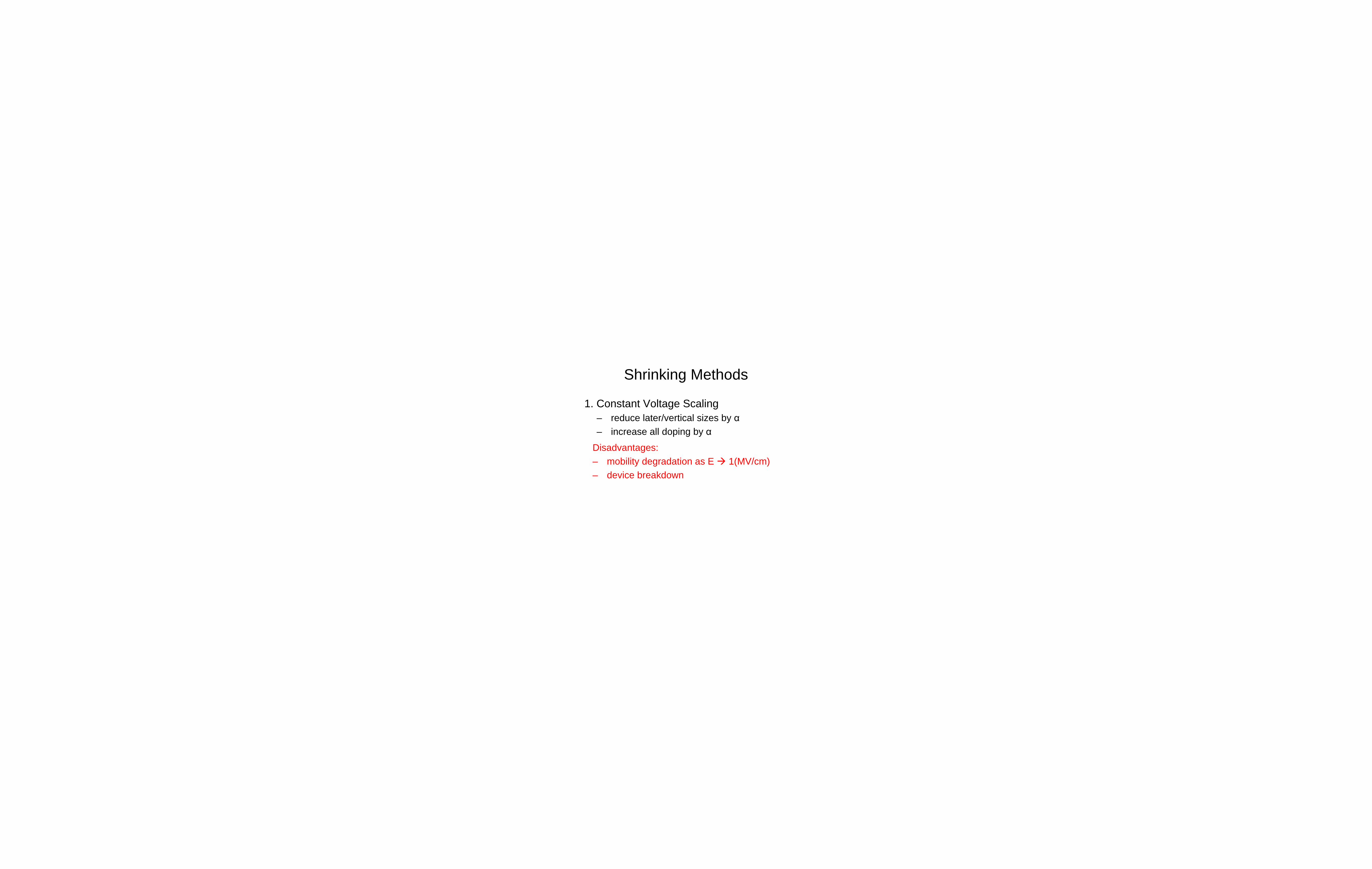
Shrinking Methods
1. Constant Voltage Scaling– reduce later/vertical sizes by α– increase all doping by α
Disadvantages:
– mobility degradation as E 1(MV/cm)
– device breakdown
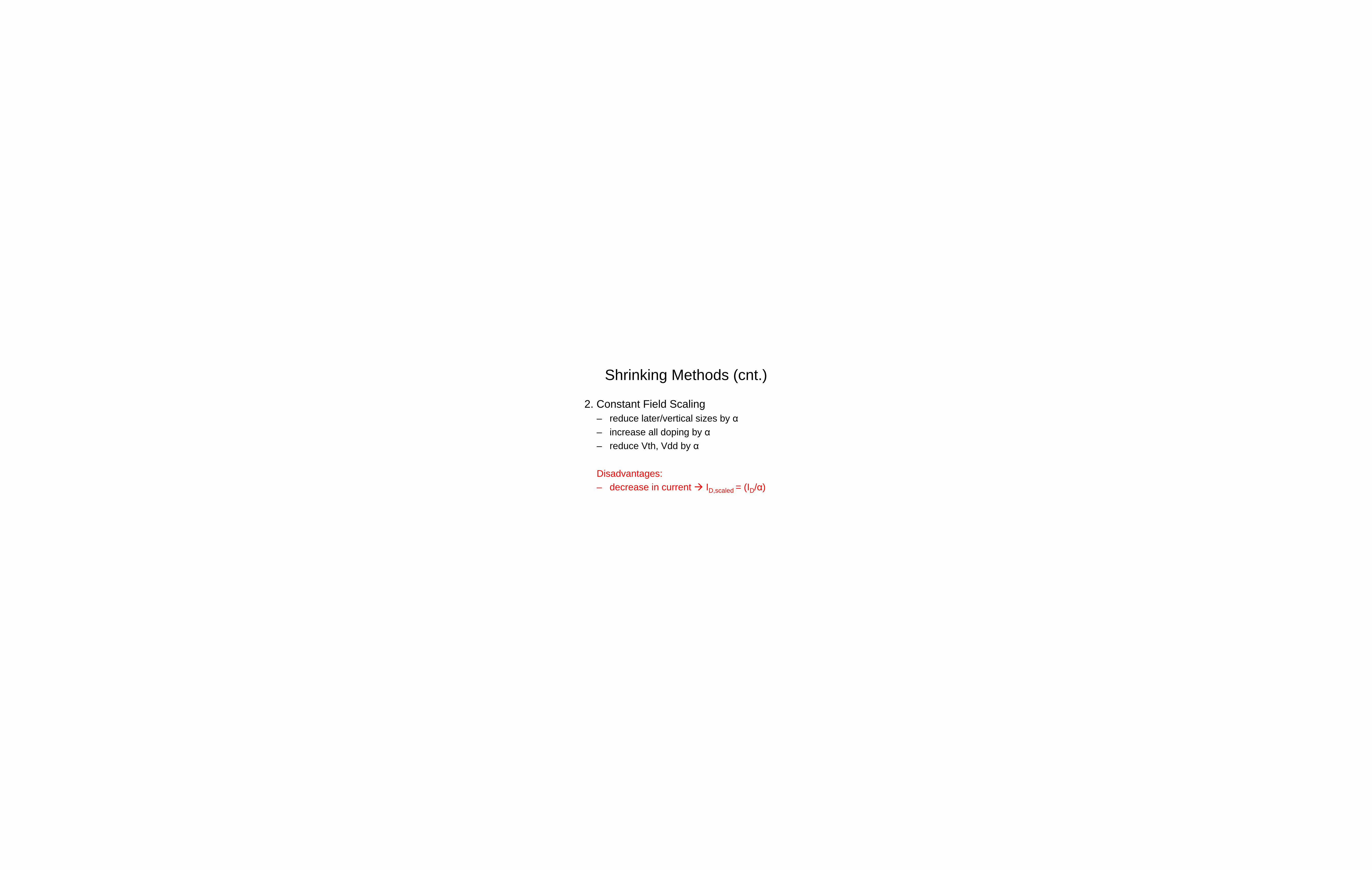
Shrinking Methods (cnt.)
2. Constant Field Scaling– reduce later/vertical sizes by α– increase all doping by α– reduce Vth, Vdd by α
Disadvantages:
– decrease in current ID,scaled = (ID/α)
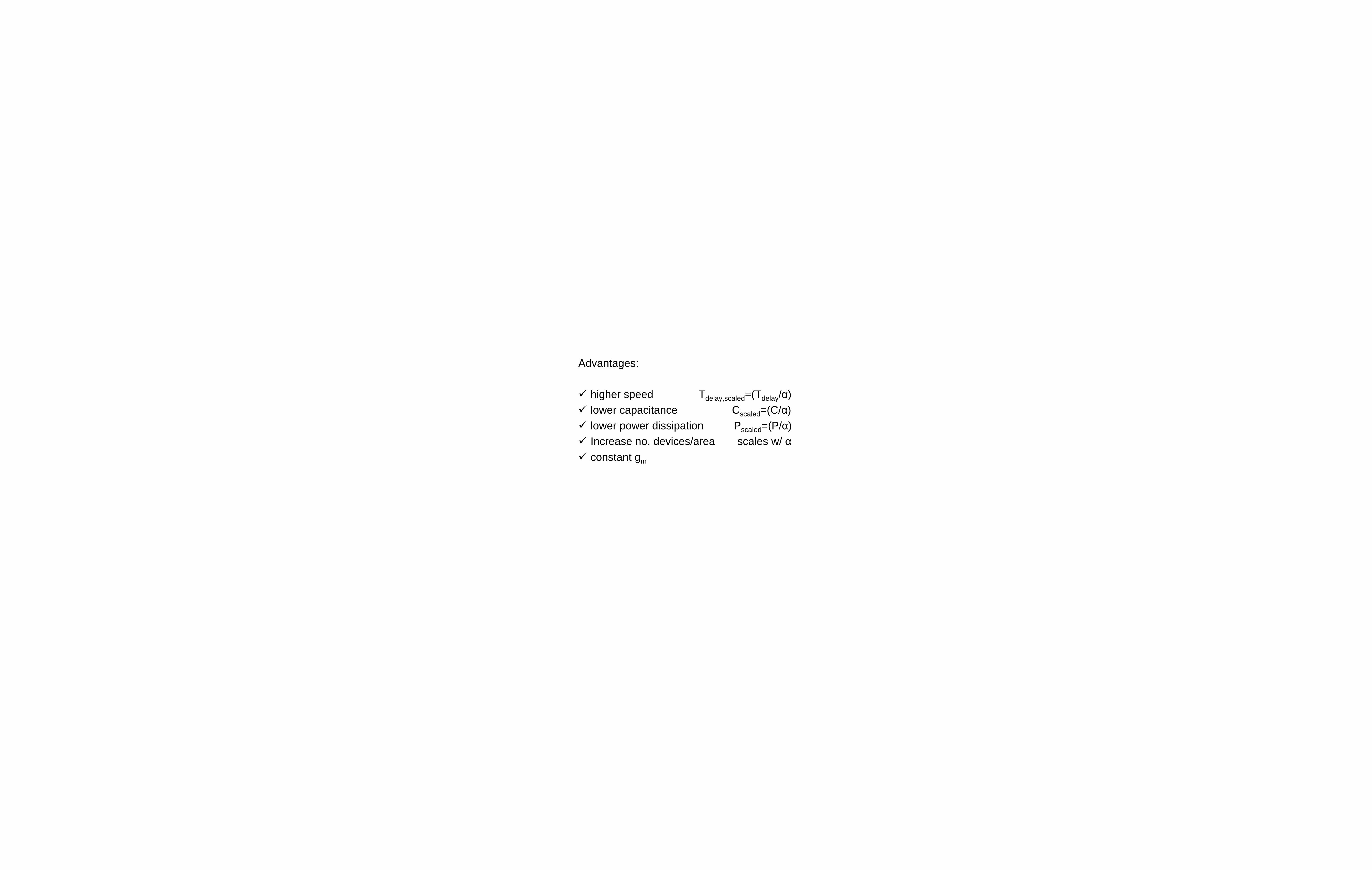
Advantages:
higher speed Tdelay,scaled=(Tdelay/α)
lower capacitance Cscaled=(C/α)
lower power dissipation Pscaled=(P/α)
Increase no. devices/area scales w/ αconstant gm
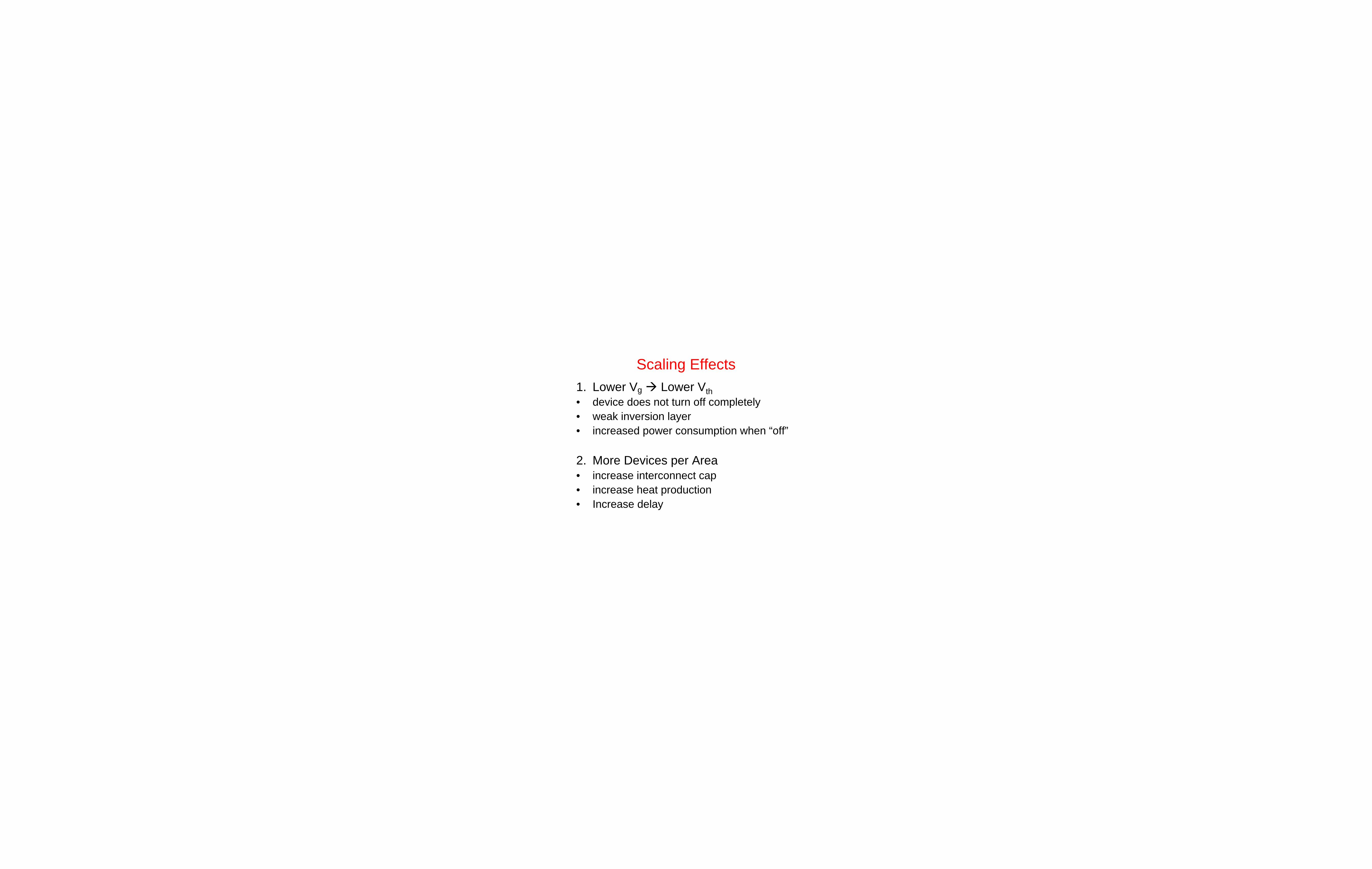
Scaling Effects
1. Lower Vg Lower Vth
• device does not turn off completely• weak inversion layer• increased power consumption when “off”
2. More Devices per Area• increase interconnect cap• increase heat production• Increase delay
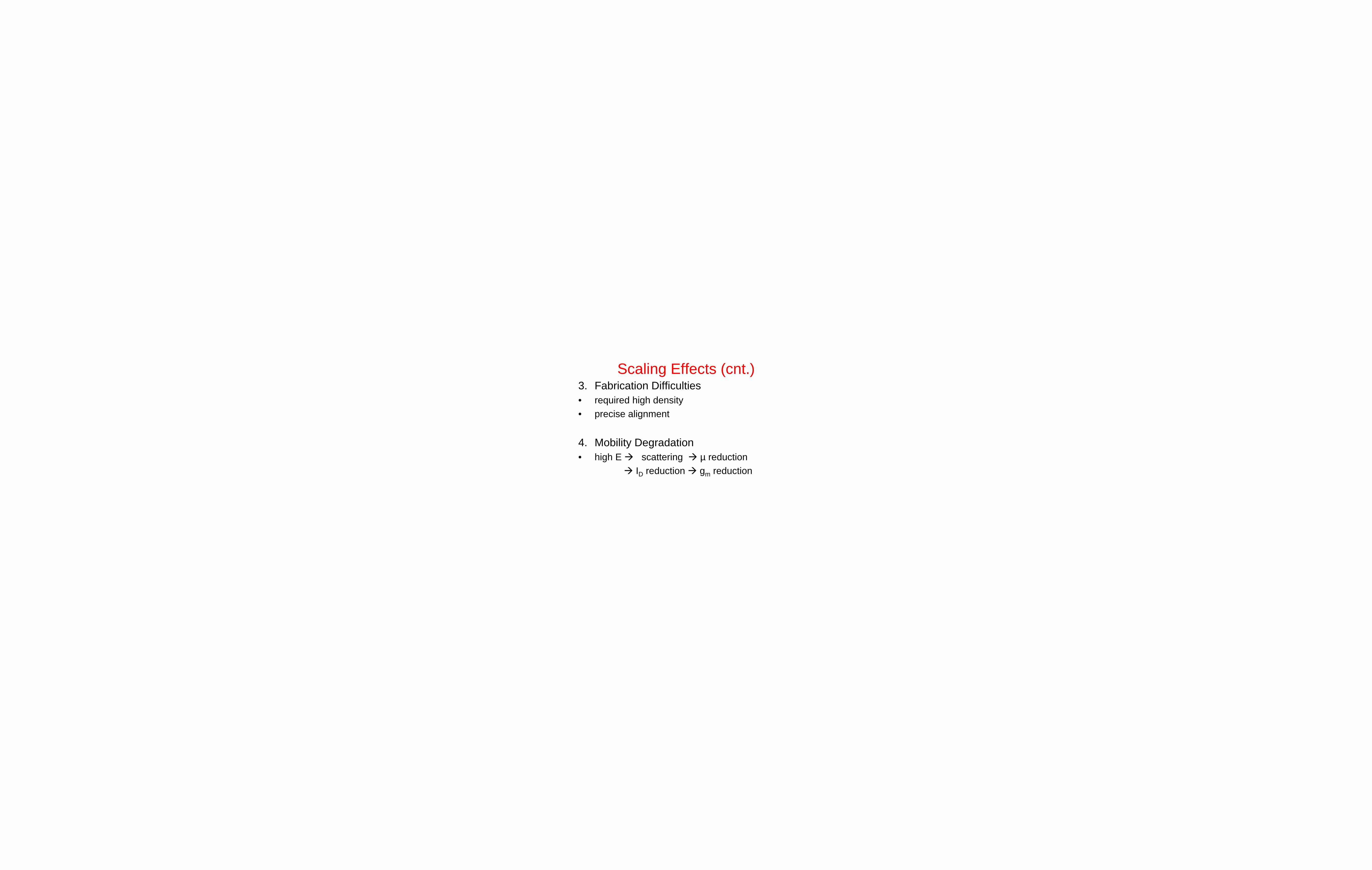
Scaling Effects (cnt.)3. Fabrication Difficulties• required high density
• precise alignment
4. Mobility Degradation• high E scattering µ reduction
ID reduction gm reduction
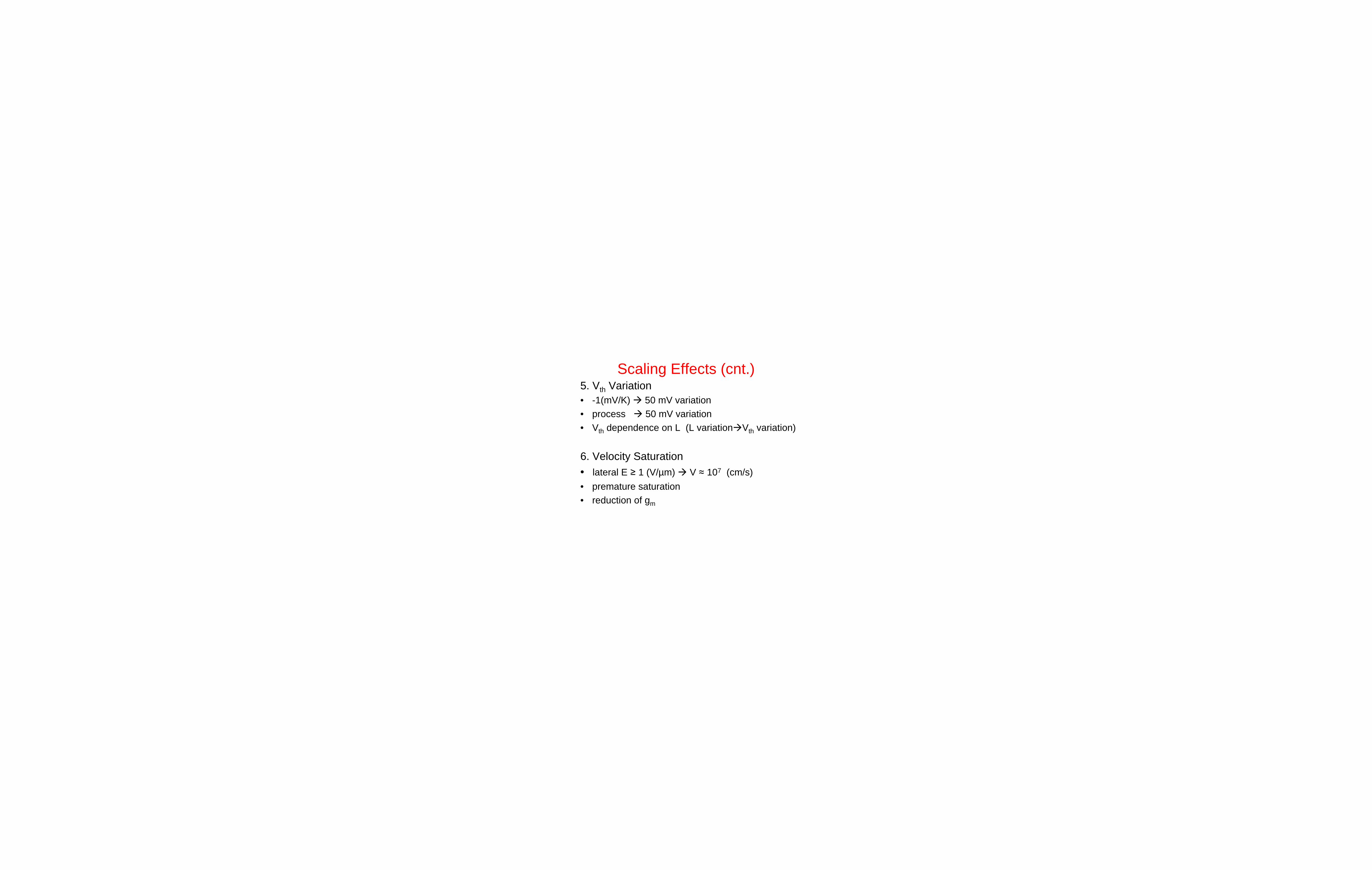
Scaling Effects (cnt.)5. Vth Variation • -1(mV/K) 50 mV variation
• process 50 mV variation
• Vth dependence on L (L variation Vth variation)
6. Velocity Saturation
• lateral E ≥ 1 (V/µm) V ≈ 107 (cm/s)
• premature saturation
• reduction of gm
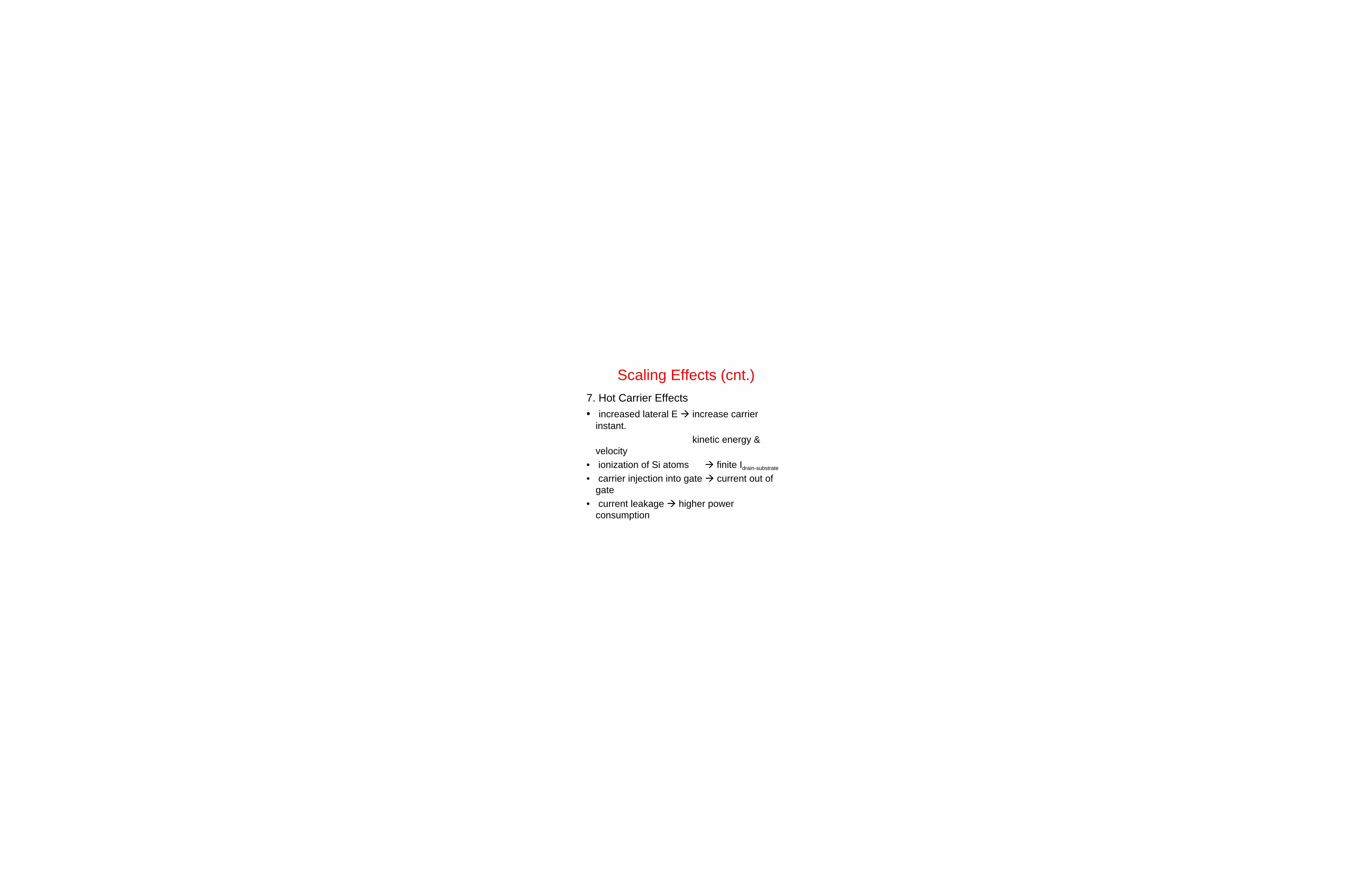
Scaling Effects (cnt.)
7. Hot Carrier Effects
• increased lateral E increase carrier instant.
kinetic energy & velocity
• ionization of Si atoms finite Idrain-substrate
• carrier injection into gate current out of gate
• current leakage higher power consumption

Scaling Effects (cnt.)8. Carrier Tunneling • high current drive reduce tox thickness
carrier tunneling through oxide
hi-k dielectric• current drive electrical thickness
• tunneling physical thickness
• Teq=(kox/k)Tphys
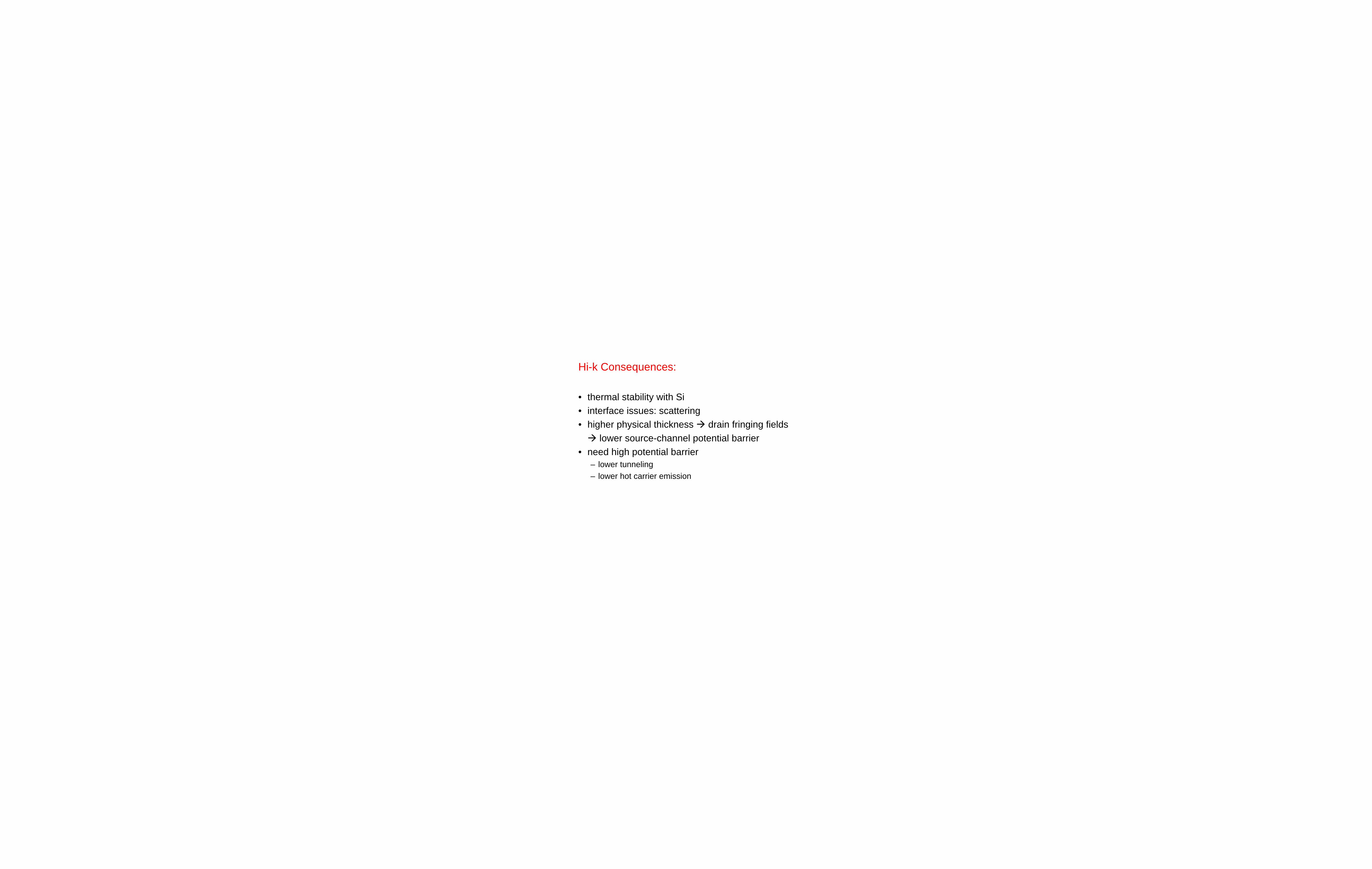
Hi-k Consequences:
• thermal stability with Si
• interface issues: scattering
• higher physical thickness drain fringing fields
lower source-channel potential barrier
• need high potential barrier – lower tunneling
– lower hot carrier emission

• ReferencesRazavi, B. Design of Analog CMOS Integrated Circuits.
New York: McGraw Hill, 2004
Wong, H.-S.P. “Beyond the Conventional Transistor.”IBM Journal of Research and Development
High κ DielectricsStephanie
High-k gate dielectrics /edited by Michel Houssa, Bristol, England; Philadelphia :IOP Publishing, c2004

What’s special about dielectrics?
• Insulators
• Material becomes polarized in an electric field
• Used to reduces the electric field between 2 surfaces of a capacitor
• The voltage across the capacitor decreases
+
--
+
--
+
--
- - - - - -
+ + + + +
E
E = −∇V
C = QV

Traditional Dielectric SiO2• Advantages
– Can be grown thermally on Si• Control over thickness and uniformity
– Stable interface with Si
– Low density of intrinsic interface defects
– Thermally and chemically stable• Manufacturing steps can involve annealing at 1000o C
– Large band gap
– Functional down to around 1.5nm

Traditional Dielectric SiO2• Problems
– Theoretical scaling limit ~7 Angstroms • Below don’t have full band gap
– Leakage due to tunneling • Tunneling proportional to exp(thickness)• 1.6 - 1.4 very thinnest that can still work with
acceptable leakage
– Defects limit thickness to around 2nm

Possible solution• High κ dielectric constant materials (greater
than SiO2)• C=Aκεο/d• Instead of increasing d further increase κ• For example:
– κ of SiO2 = 3.9– κ of Al2O3 ~ 10.0– Need a ~ 2.6 nm thick film of Al2O3 to get same
capacitance as 1nm thick SiO2

Manufacturing techniques• Atomic layer deposition • Chemical vapor deposition• Pulsed laser deposition

Atomic Layer Deposition • Thin film deposition method• Layers grown in sequence • Process steps
– 2 or more gaseous chemical reactants added to vacuum chamber
– Deposit by chemical reaction on the substrate – Purge – Repeat same or different reaction step to grow
layers
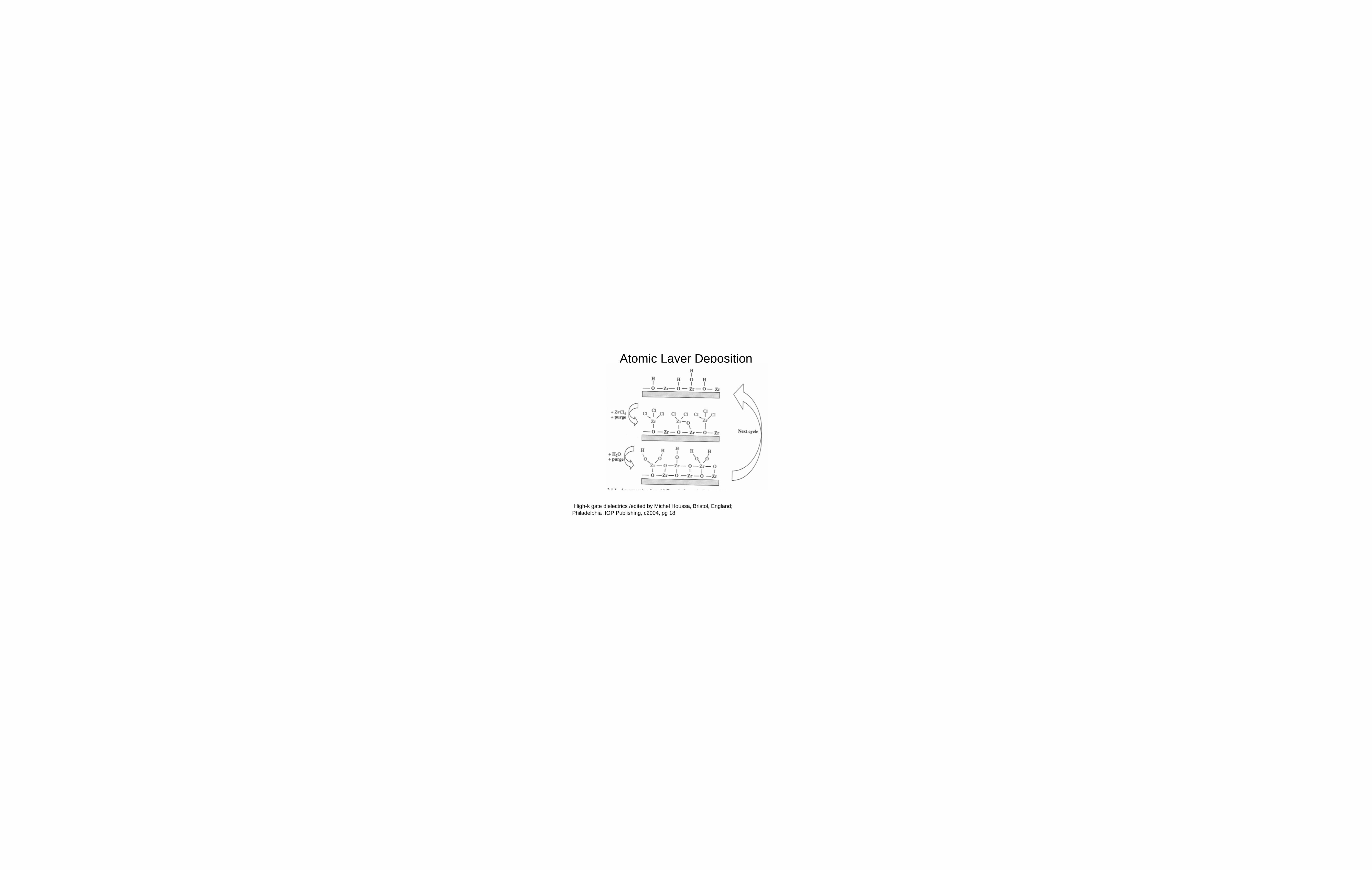
Atomic Layer Deposition
High-k gate dielectrics /edited by Michel Houssa, Bristol, England;Philadelphia :IOP Publishing, c2004, pg 18
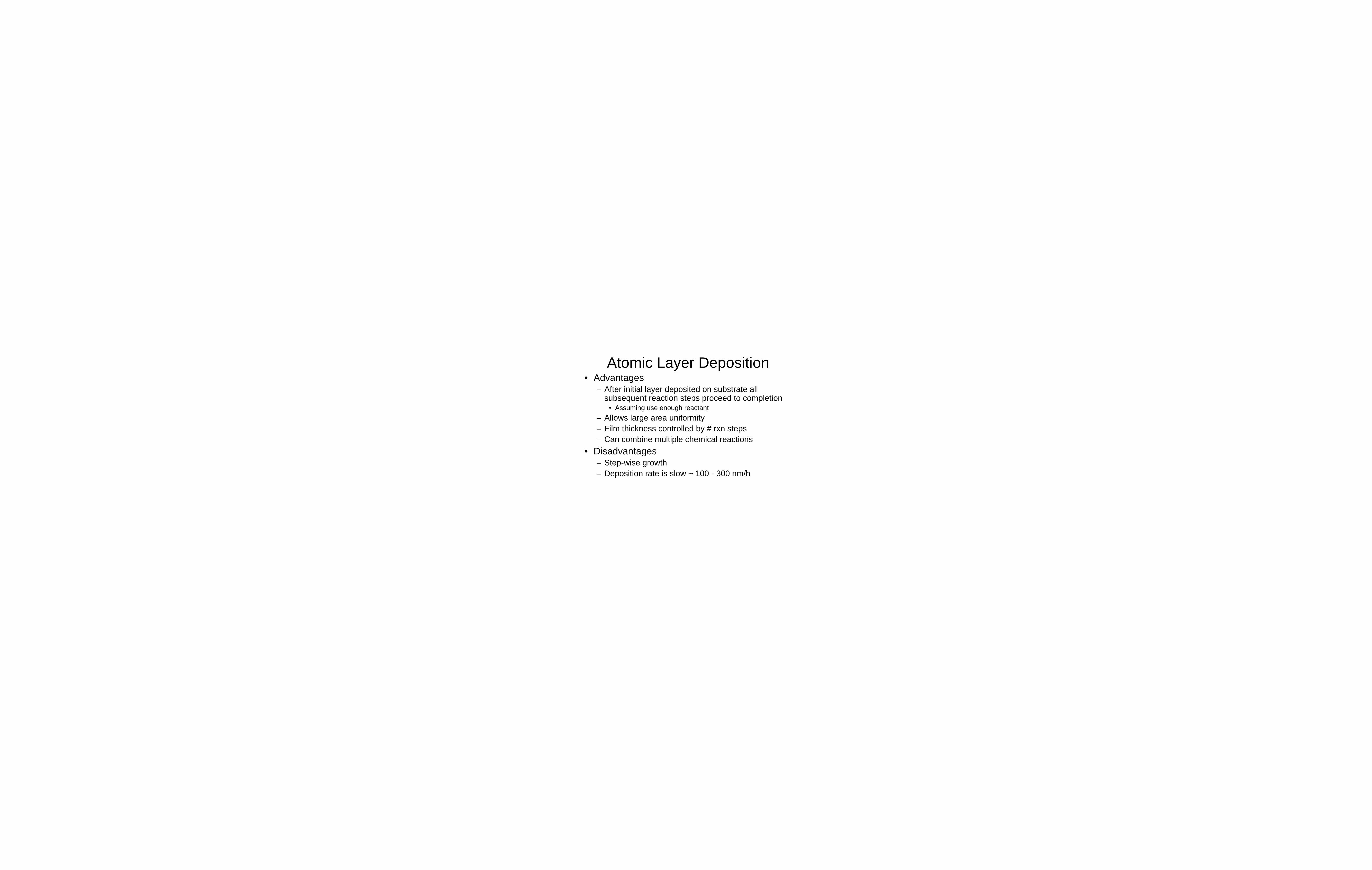
Atomic Layer Deposition • Advantages
– After initial layer deposited on substrate all subsequent reaction steps proceed to completion
• Assuming use enough reactant
– Allows large area uniformity – Film thickness controlled by # rxn steps– Can combine multiple chemical reactions
• Disadvantages– Step-wise growth– Deposition rate is slow ~ 100 - 300 nm/h

Chemical Vapor Deposition• Gaseous chemicals reactants added to
vacuum chamber• Rxn takes place in the gas phase• Rxn product and unused reactants deposit
onto heated substrate • 3 possibilities
– react with the substrate– Diffuse on the substrate – Desorb from the substrate
• Purge chamber
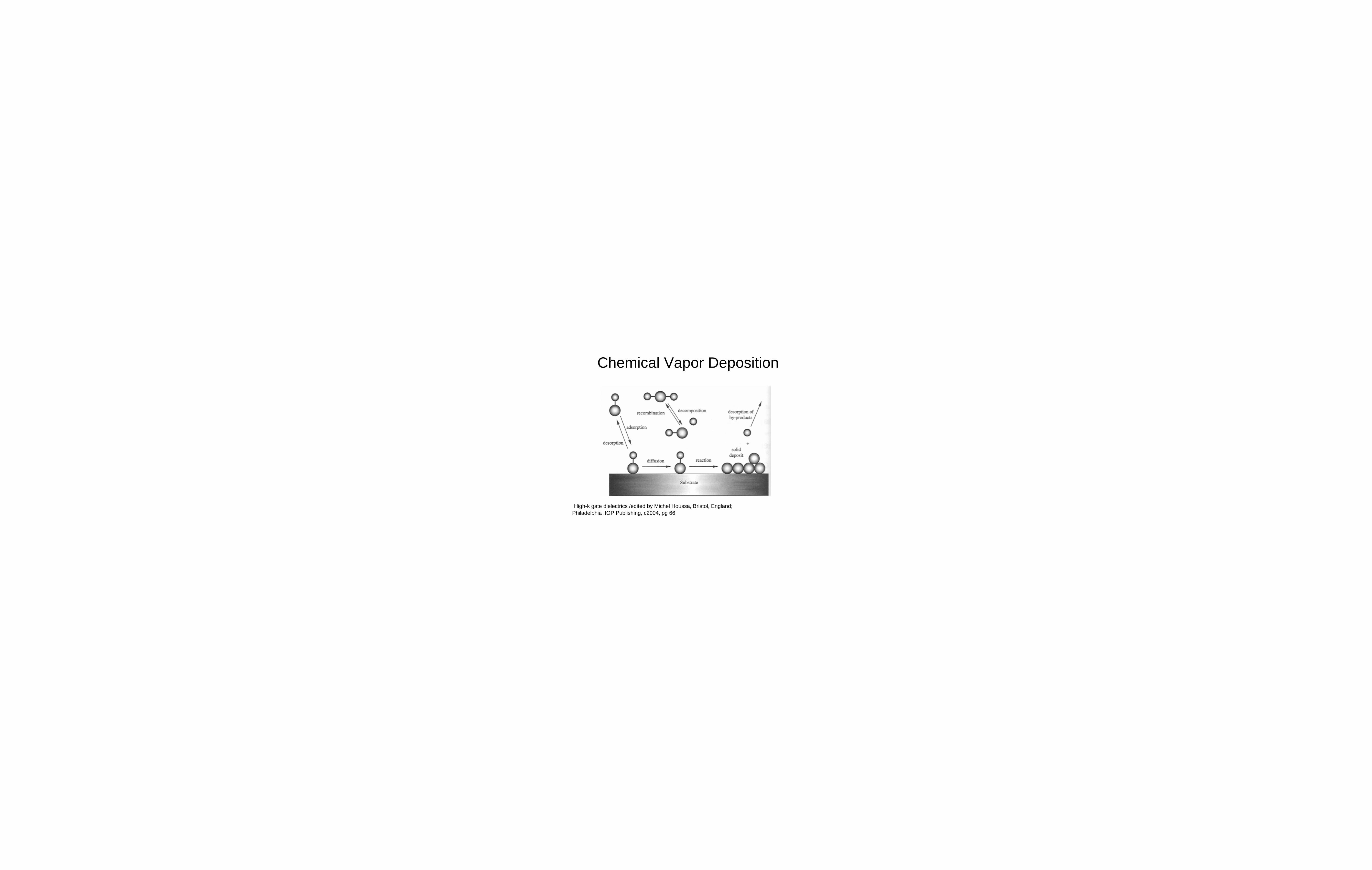
Chemical Vapor Deposition
High-k gate dielectrics /edited by Michel Houssa, Bristol, England;Philadelphia :IOP Publishing, c2004, pg 66

Chemical Vapor Deposition• Advantages
– Already used in industry – Can control deposition rates from 1 to 1000
nm/min– Can control composition
• Disadvantages– Complex chemistry – Residual impurities due to by-products of
chemicals– Extra reactants can nucleate to form particles
which deposit on the substrate surface• Effects morphology

Pulsed Laser Deposition• Heated substrate in vacuum chamber• Laser is outside chamber• Laser is focused on a source material inside chamber• Source material is vaporized • Sublimes onto substrate• Advantages
– Deposition can take place in an oxygen environment– High deposition rate– Can use higher pressures so compounds that are unstable at low
pressures can be made into dielectrics

New material properties• Same defect densities as SiO2
• Significant reduction of electron tunneling for high κdielectic materials of thickness of 1nm as compared to SiO2
• Thermally and chemically stable • Chemical stability with respect to SI
– When depositing high κ dielectric oxide onto silicon, a thin low-κ interfacial layer can form
– 1/Ctotal = 1/Clow κ + 1/Chigh κ
– Equivalent oxide thickness to give same capacitance as SiO2 increases when interfacial layer present

New material properties• 3 ranges for new dielectric materials• Ultra- high-κ (κ>100)
– Allows thickest dielectric material– Field-induced barrier lowering effect problem
• Dielectric rectangular rather than a film• Channel potential controlled be gate electrode, source and
drain & MOSFET hard to turn off
• Mid-range high -κ (10<κ<100)– Common materials in CMOS– κ not necessarily high enough to suppress gate leakage
current sufficiently compared to potential problems
• Moderate high-κ (4<κ<10)
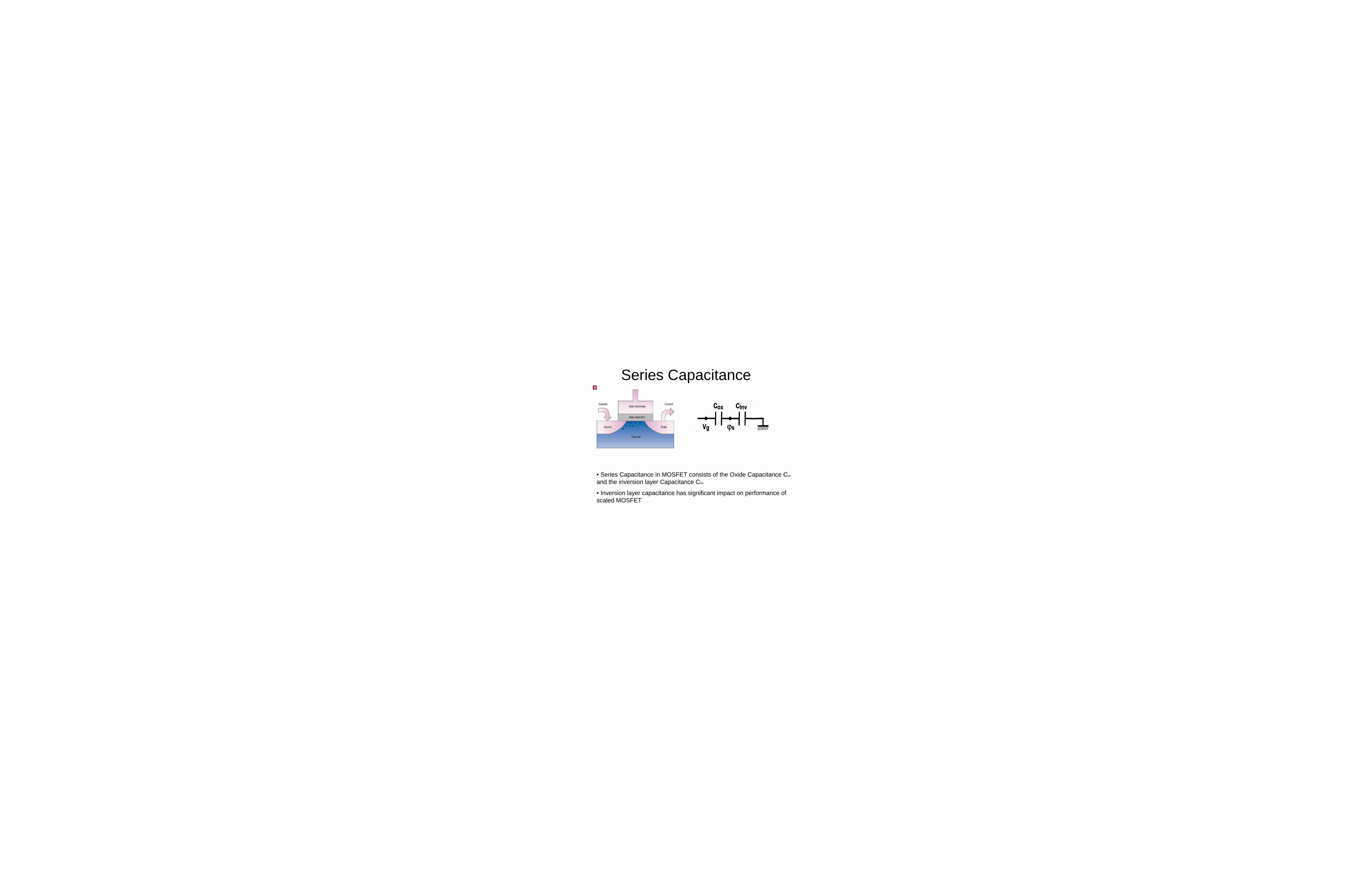
Series Capacitance
• Series Capacitance in MOSFET consists of the Oxide Capacitance Cox
and the inversion layer Capacitance Cinv
• Inversion layer capacitance has significant impact on performance of scaled MOSFET

Inversion Capacitance
• Reason: The total gate capacitance , which determines the transconductance is reduced by the inversion layer capacitance
• We can depict the Inversion layer Capacitance as follows:
• Ns is the surface carrier concentration and φs is the surface potential
•We find that at lower Ns, Cinv is determined by the finite effective density of states and at higher Ns, Cinv is determined quantum mechanically by the finite inversion thickness layer
Inversion Capacitance
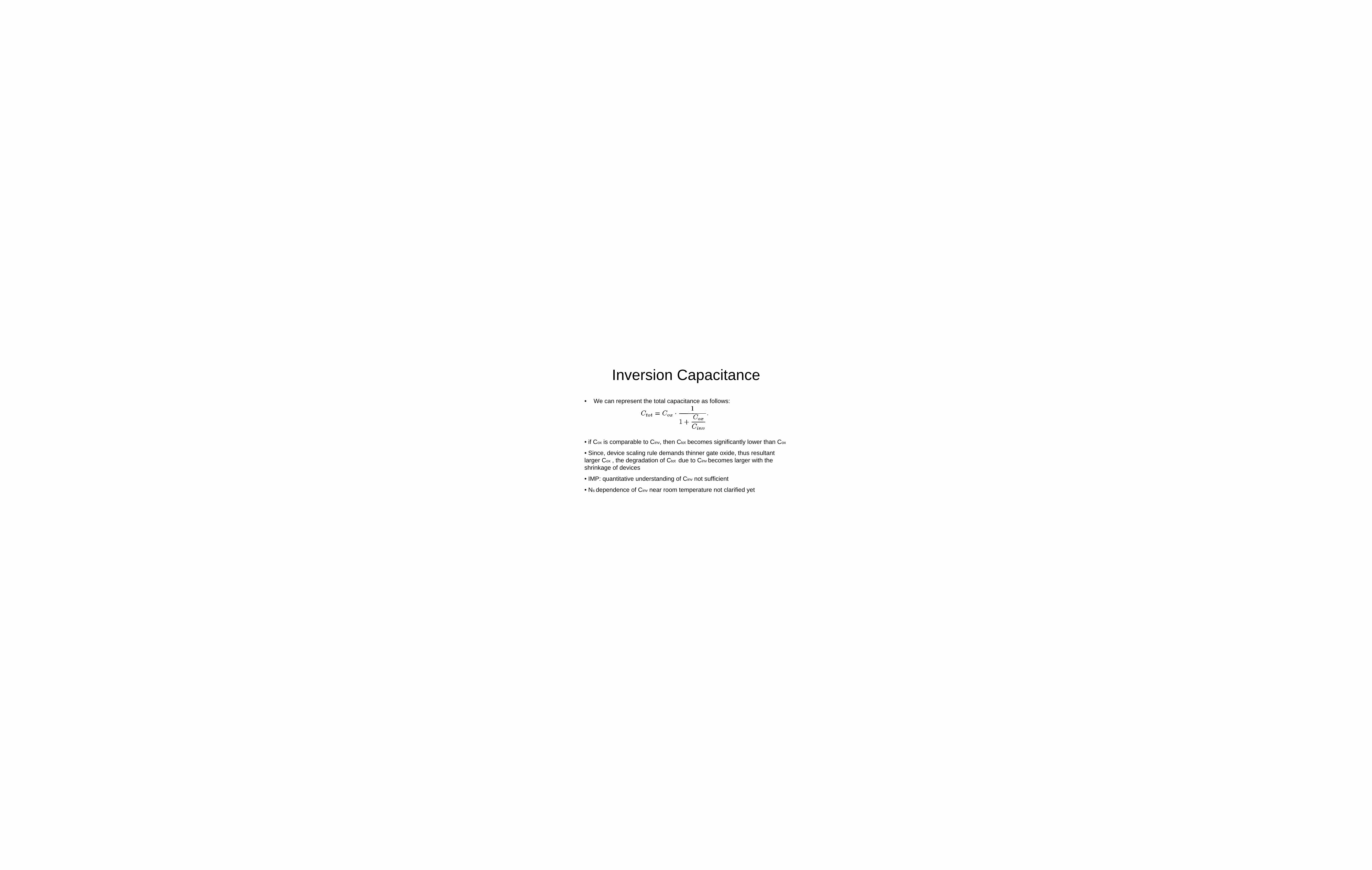
• We can represent the total capacitance as follows:
• if Cox is comparable to Cinv, then Ctot becomes significantly lower than Cox
• Since, device scaling rule demands thinner gate oxide, thus resultant larger Cox , the degradation of Ctot due to Cinv becomes larger with the shrinkage of devices
• IMP: quantitative understanding of Cinv not sufficient
• Ns dependence of Cinv near room temperature not clarified yet
Inversion Capacitance Cinv
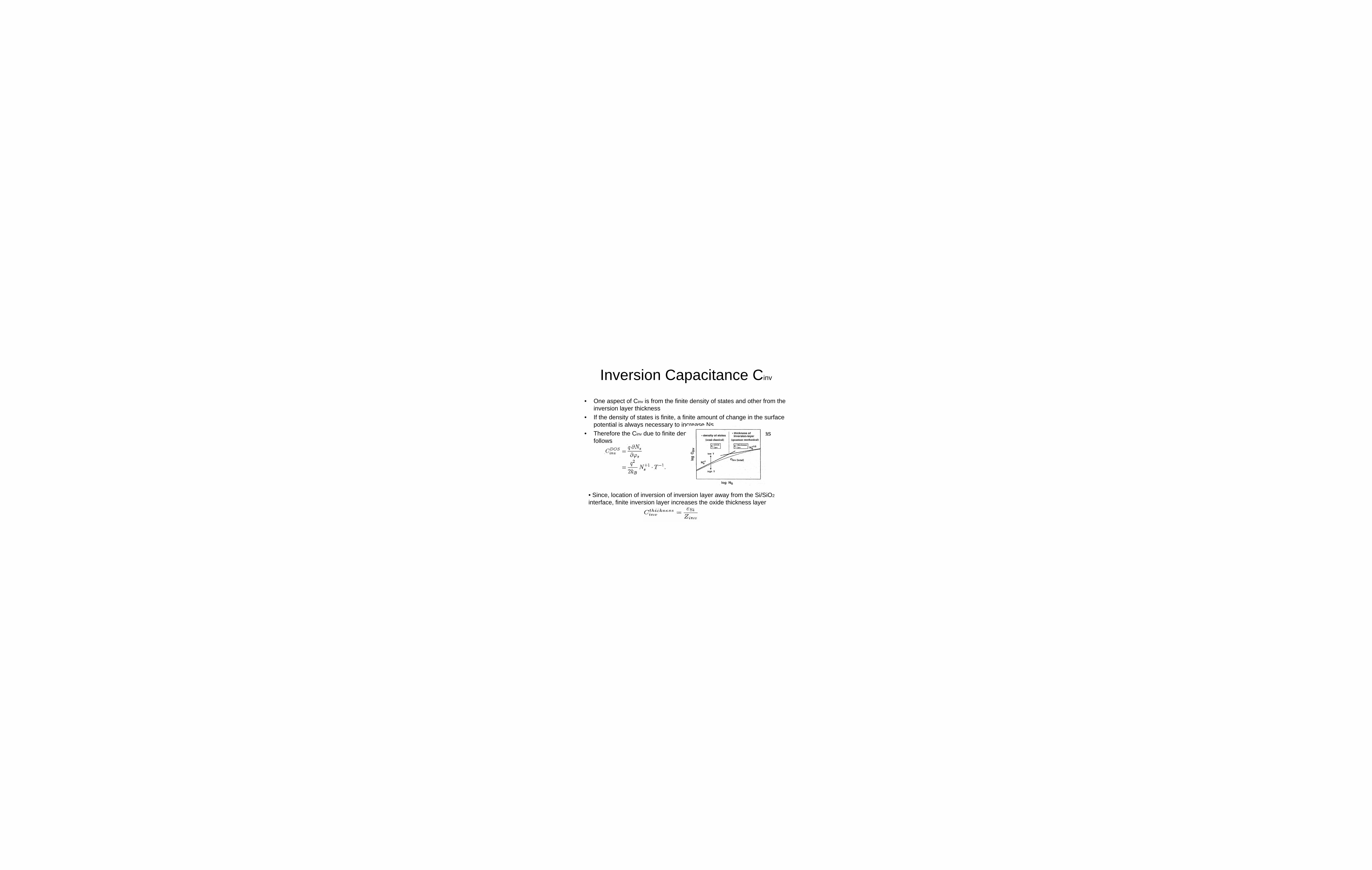
• One aspect of Cinv is from the finite density of states and other from the inversion layer thickness
• If the density of states is finite, a finite amount of change in the surface potential is always necessary to increase Ns
• Therefore the Cinv due to finite density of state can be depicted as follows
• Since, location of inversion of inversion layer away from the Si/SiO2
interface, finite inversion layer increases the oxide thickness layer

Inversion Capacitance
• Cinv thickness is independent of temperature and is in proportion to the one-third power of Ns
• Thus, in order to obtain total Cinv,
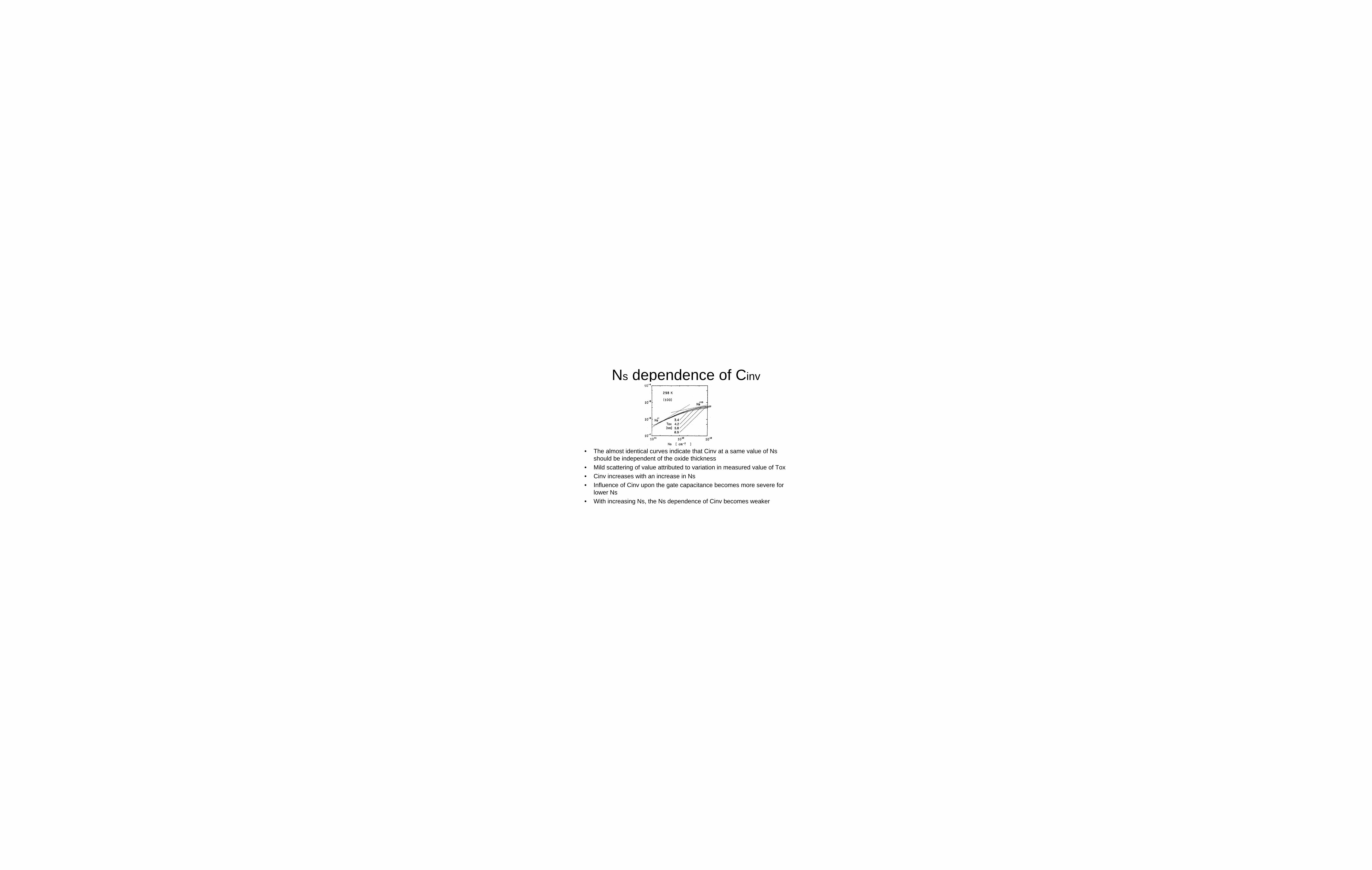
Ns dependence of Cinv
• The almost identical curves indicate that Cinv at a same value of Ns should be independent of the oxide thickness
• Mild scattering of value attributed to variation in measured value of Tox
• Cinv increases with an increase in Ns
• Influence of Cinv upon the gate capacitance becomes more severe for lower Ns
• With increasing Ns, the Ns dependence of Cinv becomes weaker

Temperature dependence of Cinv
• As the temperature increases, the Cinv in lower Ns regions becomes smaller and the Ns dependency approaches close to linear dependence
• At higher temperatures, the Cinv is almost inversely proportional to T

Leakage Currents
• When the gate oxide of the MOSFET breaks down, a leakage path iscreated between channel and gate
• When gate oxide is ultra thin, the first breakdown is a soft breakdown
• As long as the power supply can cope with the additional load due to the leakage current, an inversion layer will still form in the channel and the transistor will function properly
• Even when one or more transistors show a soft breakdown, the circuit may not fail if the circuit can tolerate the reduced performance levels
• Even hard breakdown has shown not to cause failure if the leakage current is not too high

Current CMOS Design
• CMOS Design basics have not changed
• Performance and scalability issues are resolved by tweaking the design
• Different techniques are being used to extend the lifetime of the Planar CMOS

Silicon on Insulator
• Primarily used by AMD and IBM
• Addition of insulator reduces current leakage and increases switching speed
• Technology has been around since the 1940s
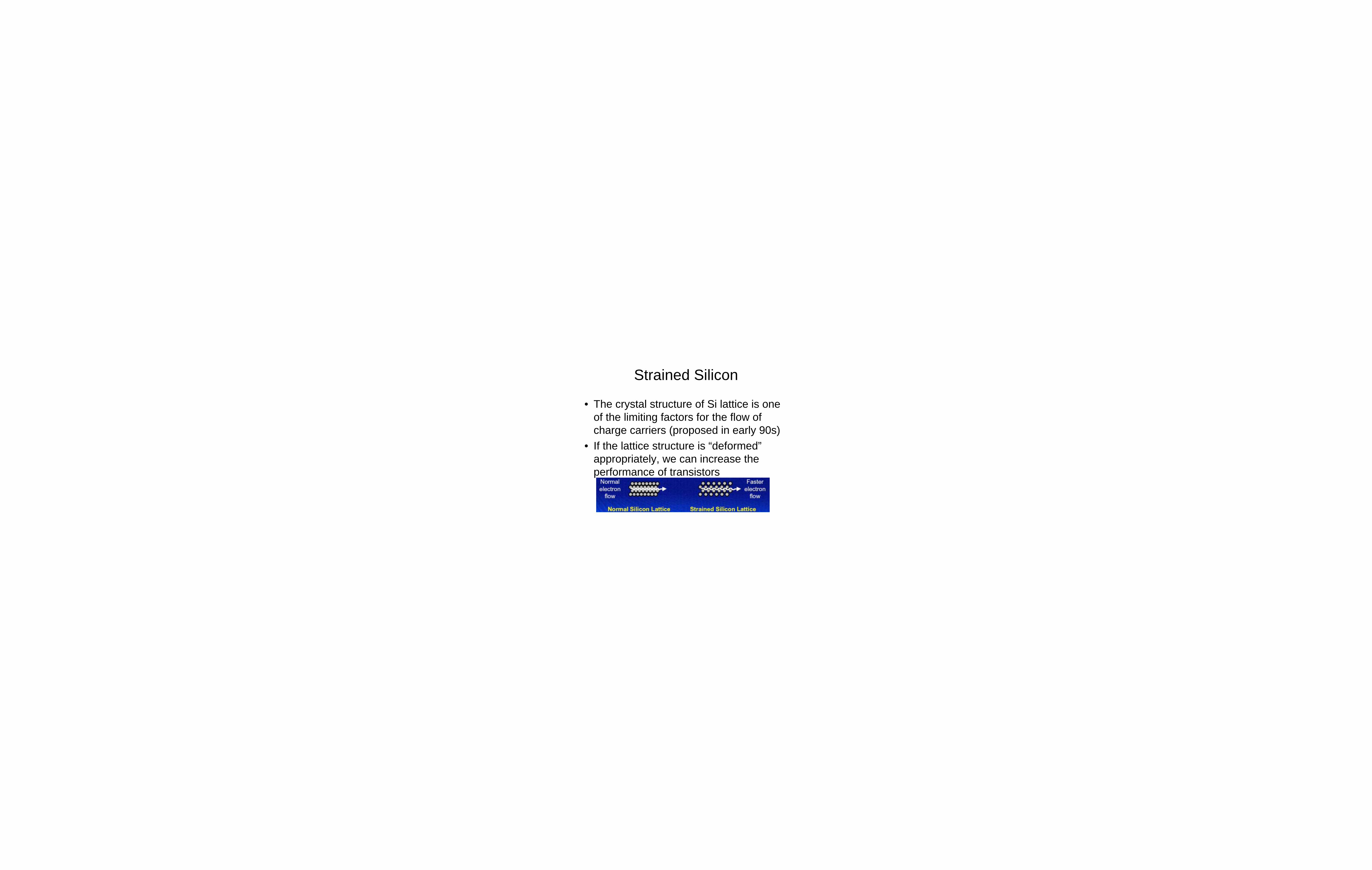
Strained Silicon
• The crystal structure of Si lattice is one of the limiting factors for the flow of charge carriers (proposed in early 90s)
• If the lattice structure is “deformed”appropriately, we can increase the performance of transistors
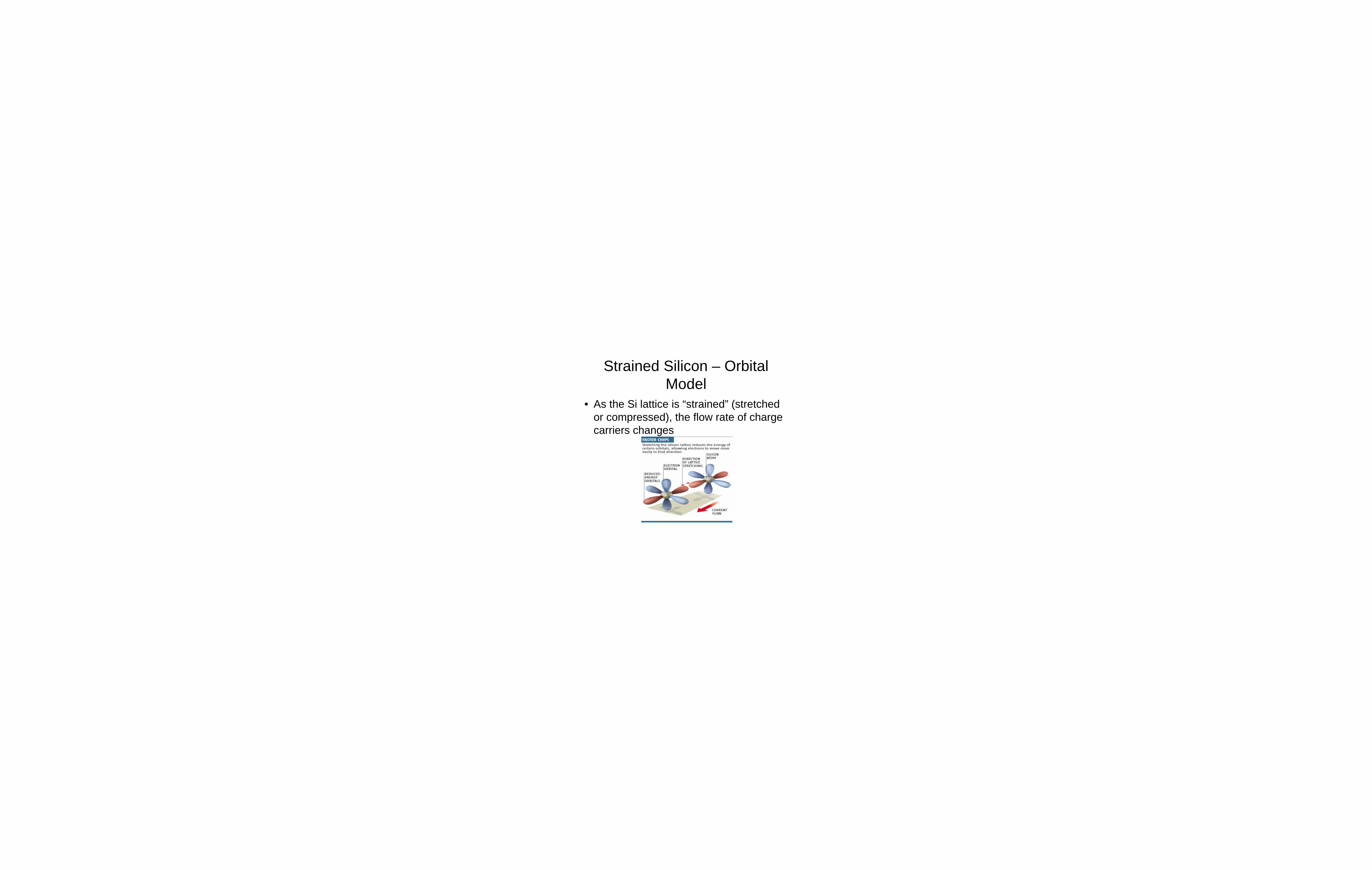
Strained Silicon – Orbital Model
• As the Si lattice is “strained” (stretched or compressed), the flow rate of charge carriers changes
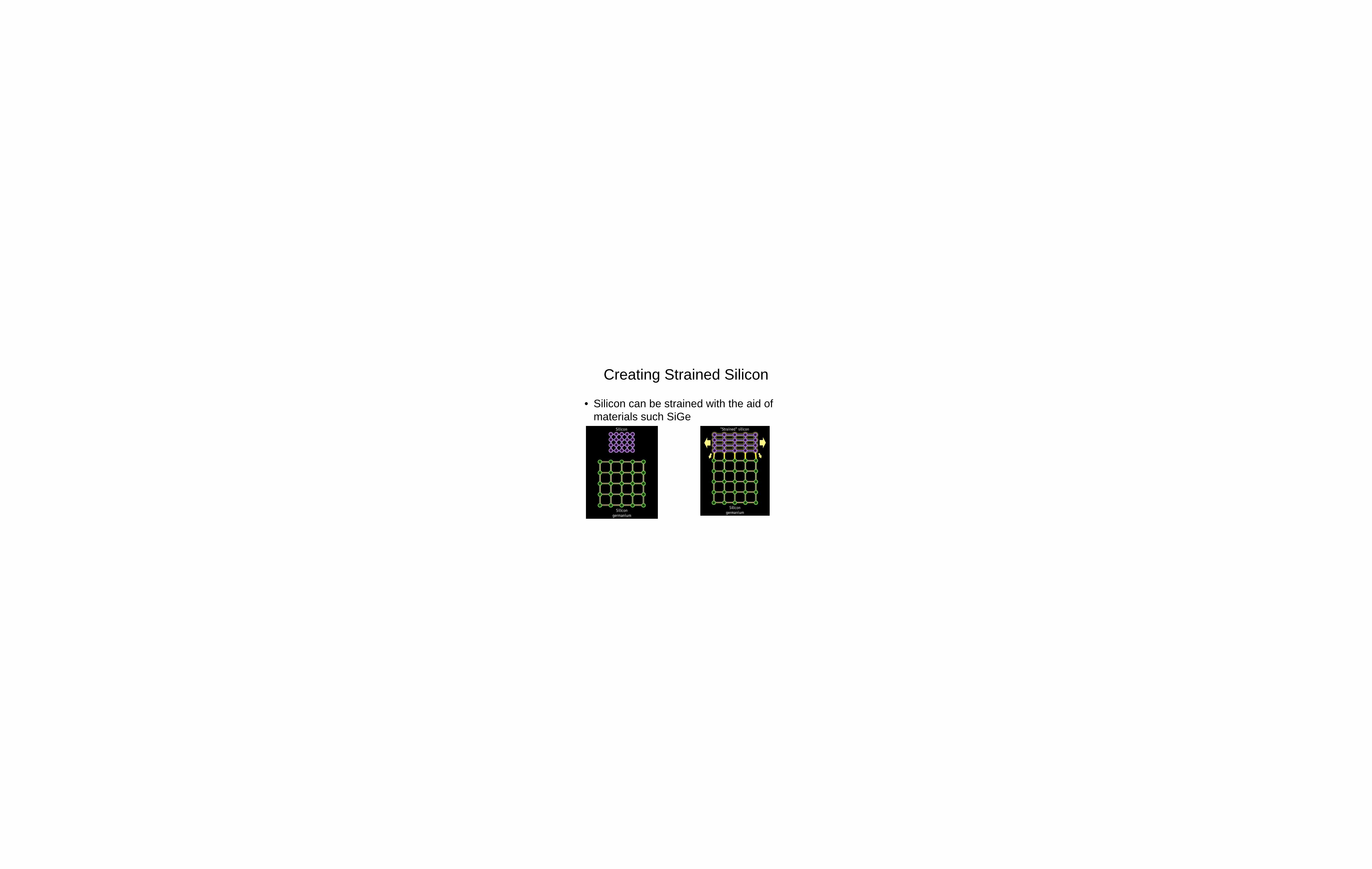
Creating Strained Silicon
• Silicon can be strained with the aid of materials such SiGe

Strained Si Demo
• Movie time.

Other Techniques
• A combination of techniques has saved the CMOS transistor from going extinct
• Planar transistors are expected to be out of date at the 45 – 32 nm manufacturing level
• A possible replacement for planar transistors is the FinFET (3D Transistors)
• Intel and AMD have proposed the use of Tri-gate transistors

FinFET
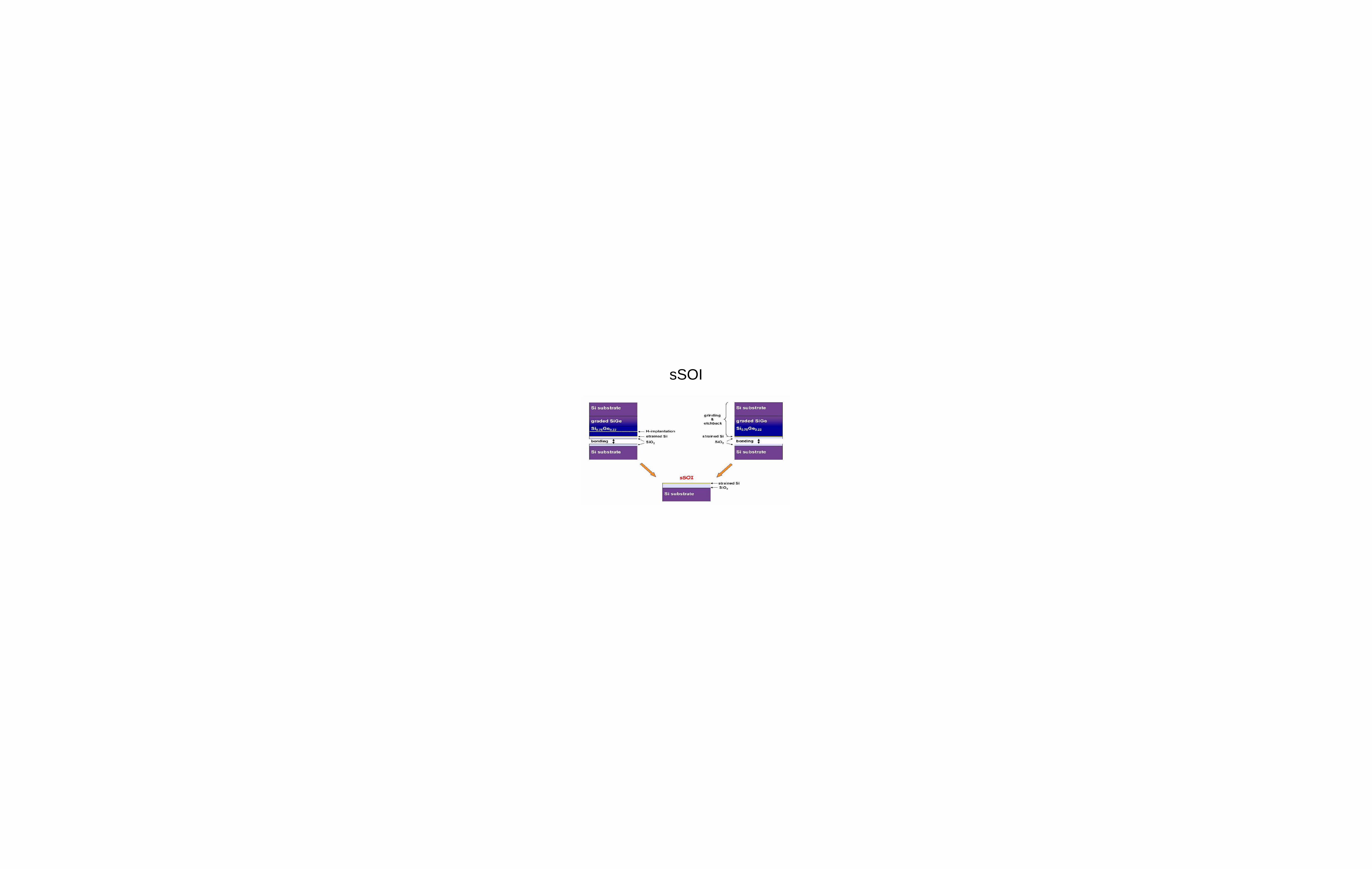
sSOI

Q/A
• Questions?

Recommended