Winter 2005www.svc.org
NewsNews
A P u b l i c a t i o n f o r t h e V a c u u m C o a t i n g I n d u s t r yA P u b l i c a t i o n f o r t h e V a c u u m C o a t i n g I n d u s t r y
Smart MaterialsSneak Preview:
Large-ScaleOrganicPhotovoltaics
Smart MaterialsSneak Preview:
Large-ScaleOrganicPhotovoltaics
2005 TechConProgram Report
2005 TechConProgram Report
New!Original article on the
Fundamentalsof Optical Coatings
New!Original article on the
Fundamentalsof Optical Coatings
2005 Winter News Bulletin 3
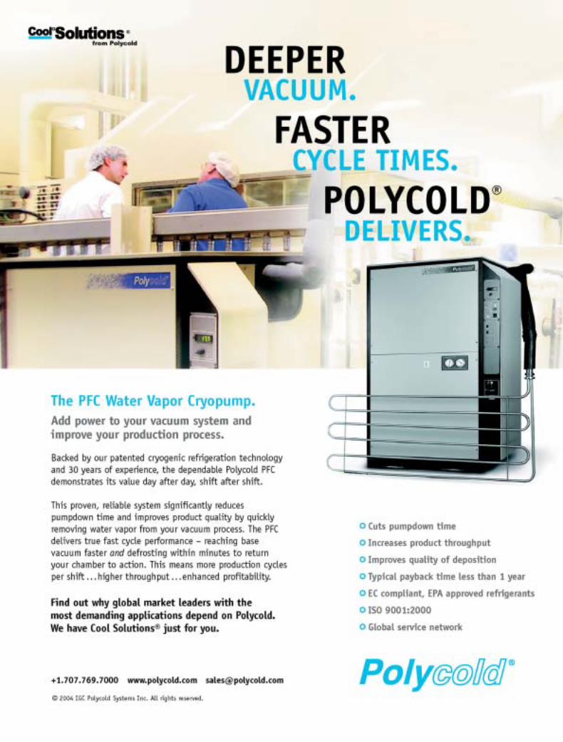
Inside This Issue
Plasma Processing
Sandia's Pauline Ho checks processing of components in her PlasmaProcessing Research Laboratory. Plasmas are hot gases used to etch circuitson microchips and to clean the surfaces of components to enhance adhesion.
Photo by Randy Montoya, Sandia National Laboratories
On the Cover
Letter from the President . . . . . . . . . . . . . . . . . . . . . . . . . . . . . . . . . . . . . . 4
Editorial. . . . . . . . . . . . . . . . . . . . . . . . . . . . . . . . . . . . . . . . . . . . . . . . . . . . 4Plasma Fusion: What can we learn?by Donald M. Mattox
SVC Technical Program Report . . . . . . . . . . . . . . . . . . . . . . . . . . . . . . . . . . 5Highlights include:• From the Program Chairs . . . . . . . . . . . . . . . . . . . . . . . . . . . . . 5• Win a $200 Cash Award for Best Poster . . . . . . . . . . . . . . . . . . 7• A Vacuum Wizard’s Guide to Understanding Vacuum and
Vacuum Coating. . . . . . . . . . . . . . . . . . . . . . . . . . . . . . . . . . . . 8• Special Joint Session: Processes, Materials, and Systems for
Flexible Electronics and Optics . . . . . . . . . . . . . . . . . . . . . . . . . 8• Special Joint Session: Plasma Processing of Webs. . . . . . . . . . . . 9• Special Session on HIPIMS . . . . . . . . . . . . . . . . . . . . . . . . . . . 11 • 2nd Annual Smart Materials Symposium. . . . . . . . . . . . . . . . . 12• Workshop on Specialty Coatings. . . . . . . . . . . . . . . . . . . . . . . . 13• SVC TechCon Plenary Address presented by Salil Pradhan . . . . 14• Donald M. Mattox Tutorial Program . . . . . . . . . . . . . . . . . . . . 17• SVC Equipment Exhibit. . . . . . . . . . . . . . . . . . . . . . . . . . . . . . 18• Education Program Schedule at TechCon . . . . . . . . . . . . . . . . 20• SVC History Committee News. . . . . . . . . . . . . . . . . . . . . . . . . 21• SVC TechCon Meeting Schedule . . . . . . . . . . . . . . . . . . . . . . . 21• SVC TechCon Keynote Presentation by Zhenan Bao. . . . . . . . . 27
Smart Materials Sneak PreviewLarge Scale Organic Photovoltaics . . . . . . . . . . . . . . . . . . . . . . . . . . . . . . 15
by Frederik C. Krebs
Sample Education Guide. . . . . . . . . . . . . . . . . . . . . . . . . . . . . . . . . . . . . . 24Safety: Safety Aspects of Vacuum Processingby Donald M. Mattox
Report on Plasma Surface Engineering (PSE) 2004 . . . . . . . . . . . . . . . . . 26by Ric Shimshock, MLD Technologies LLC
Fundamentals of Optical Coatings. . . . . . . . . . . . . . . . . . . . . . . . . . . . . . 28contributed by Angus Macleod, Thin Film Center Inc.
From the 2004 SVC Technical Conference ProceedingsAdhesion Promotion Techniques for Coating of Polymer Films . . . . . . . . 34
by Rolf Rank, Tilo Wuensche, Matthias Fahland, Christoph Chartonand Nicolas Schiller, Fraunhofer Institute for Electron Beam and PlasmaTechnology
Society and Industry News . . . . . . . . . . . . . . . . . . . . . . . . . . . . . . . . . . . . 38Corporate Sponsor News . . . . . . . . . . . . . . . . . . . . . . . . . . . . . . . . . . . . . 39Corporate Sponsor Profile. . . . . . . . . . . . . . . . . . . . . . . . . . . . . . . . . . . . . 40Advertiser’s Index . . . . . . . . . . . . . . . . . . . . . . . . . . . . . . . . . . . . . . . . . . . 42
Page 8 Page 7 Page 15 Page 20
Editorial
Plasma Fusion: What can we learn?
There is a tendency for persons working in a particular area to only readmaterial on that subject. Often related material can be found in other
subject areas. This article discusses some of the work done on the subject ofplasma fusion that may be of interest to persons studying plasmas as relatedto plasma-based vacuum coating processes.
In the 1970s and 1980s a great deal of work was performed on plasmafusion—an attempt to generate energy by the fusion of deuterium (2H) andtritium (3H) in very high-temperature plasmas. Fusion is the basic methodby which the sun generates energy and was described by Hans Bethe justbefore WWII. In the 1960s the Russians developed a toroidal magneticallyconfined plasma reactor, called a TOKAMAK, that ultimately allowedattaining plasma temperatures of greater than 100M K, the temperatureneeded for a fusion reaction.
Several problems are important in attaining high plasma temperaturesthat are relevant to vacuum coating. The first is contamination in thehydrogen plasma. The higher the atomic number (Z) of the contaminant, themore the cooling effect on the plasma. There have been a number of studieson how to clean the walls of the vacuum chamber. The result has been theuse of hydrogen plasma cleaning using detection of C-H species in theexhaust gas as the indicator of the degree of removal of hydrocarbon contami-nation.
Stability of the confined plasma is another concern. When instabilitiesoccur, the plasma may hit the wall, causing ejection of high-Z contaminants.These high-Z materials become ionized in the plasma and then strike thewalls, causing “self-sputtering”. Self-sputtering has been the subject of manystudies by the fusion plasma community.
One potential solution to the plasma instability problem was tointroduce low-Z “limiters” on the walls of the vacuum chamber. Theselimiters would prevent the plasma from striking the chamber walls. Theideal limiter material would be beryllium, but that was judged as being toomuch of a health hazard so the most common limiter material is carbon.
Unfortunately, carbon erodes rapidly under hydrogen ion bombardment.In the mid 1970s it was considered that high-temperature, low-sputtering-
yield coatings on the limiters were not feasible because of the high thermalpulses present. However, it was shown that carbide coatings could beapplied to the carbon that could withstand thousands of thermal pulsesintroduced by pulsed high-energy e-beam bombardment. When the carbidecoating was placed on a ductile material (Cu), the thermal cycling causedinterfacial failure due to “ratcheting” of stress voiding.
Another potential solution was to coat the vacuum chamber walls witha renewable carbon coating. This reduced the Z of the material eroded fromthe walls. The carbon coating was periodically deposited and renewed bydecomposing a hydrocarbon vapor in a low-energy argon plasma.
Another problem was retention of hydrogen (particularly the radioac-tive hydrogen isotope, tritium) in the vacuum materials. This “plasmahydrogen charging” has been studied for a number of materials, particularlycarbon. It was also found that the structure of “redeposited” material(material that had been sputtered and then redeposited) has a large effecton hydrogen retention. This is due to both the deposit morphology(columnar) and the lattice defects (vacancies, grain boundaries, etc.) in thedeposited material.
Charging (“subplantation” is a term that is now commonly used) of amaterial with a bombarding gas (ions) has been studied for a number ofreasons. One of the earliest applications (Chleck et al 1963) was forcharging gas turbine surfaces with radioactive krypton (85Kr) (Chleck calledthese charged materials “kryptonates”). By determining the thermal desorp-tion spectrum after heating, the maximum temperature that portions of thesurface has seen in service can be determined. The energy for thermaldesorption is determined by the type of lattice defect binding the 85Kr atom.Deposition of film material with concurrent gaseous bombardment has beenused to study “storing” of gases in film structures (Mattox et al, 3He –1971;Cuomo et al, 85Kr – 1977).
It is interesting to note that what is now the Plasma Science Division ofthe AVS Science and Technology Society started out as the Plasma FusionDivision. References to self-sputtering and other fusion technology problemsmay be found in Journal of Vacuum Science and Technology, RadiationEffects, Journal of Nuclear Materials, and other journals.
by Donald M. Mattox, SVC Bulletin Editor and Technical Director
4 2005 Winter News Bulletin
Letter from the President
Happy New Year! I hope you had a greatholiday season and are looking forward to a
wonderful 2005. We are looking forward to theannual SVC Technical Conference (TechCon) tobe held from April 23 to 28, 2005, at the Adam’sMark Hotel in Denver, CO. Put those dates onyour new calendar now. Also, look for thePreliminary Program describing the outstandinglineup of technical presentations andeducational courses, plus the bonus SmartMaterials Symposium.
As part of the Board’s fiduciary responsi-bility, an industry benchmarking process and acompetitive bidding process were used to selecta management organization for SVC. I am happyto report that we have signed a letter of intentfor a new management contract withManagement Plus, Inc. (MPI). We are finalizingthe details of this contract, which will be in placeby the end of January. Vivienne and Don Mattoxand their team have managed our Society forover 16 years and deserve much of the credit for
our success. We are delighted to have themcontinue as our management company. We lookforward to implementing their plans for anoperational structure to grow with the Society inthe future.
I want to welcome four newly electedDirectors to the SVC Board: David Christie,Wolfgang Decker, Vasgen Shamamian, and EdWegener. These Board members help representthe diversity of our Society membership, and willbring fresh viewpoints. Dave and Wolfgang areregular speakers at the TechCon but new to theleadership of our Society. Vasgen has been activeas the Plasma Processing Technical AdvisoryCommittee (TAC) Chair, and Ed previouslyserved as a Board member, is Chair of theInvestment Committee, and most recently servedas Treasurer. Please congratulate them on theirelection.
Also, I want to thank the outgoing Boardmembers for their dedicated service to SVC.Directors whose terms expire at the TechCon are
Liz Josephson, Traci Langevin, and RicShimshock. They all have contributed signifi-cantly as Board members to the success of ourSociety. Of course, they continue helping theSociety in other capacities. Liz is Chair of theInternational Relations Committee; Traci is Chairof Foundation Fund Raising; and Ric is our 2005TechCon Program Chair and PublicationsCommittee Chair.
SVC enters 2005 in excellent financialcondition, technically strong, and well managedthanks to the efforts of MPI, our volunteers, andthe support of our dedicated membership andTechCon exhibitors. As always, I ask for yourparticipation in influencing the course of SVC.Join a TAC or other committee or run for theBoard and become an Officer. We need yourideas, help, and support in facing new challengesfor the Society in 2005 and beyond.
Clark Bright, 3M Company ([email protected]), isthe SVC President.
2005 Winter News Bulletin 5
SVC Technical Program Report
Get ready for Denver!
Be sure to include the upcoming 48th AnnualSVC 2005 TechCon in your plans for this spring.Make your travel arrangements and get yourhotel reservations. You won’t want to miss theSVC’s premier information exchange andnetworking event. The 2005 SVC TechConconvening in Denver on April 23–28 promises tobe one of the best ever! We have assembled avery full program of offerings. Our EducationalProgram has been expanded with new courses;our TechCon is once more scheduled over thecourse of four days packed with must-see presen-tations; and we have programmed three specialjoint TechCon sessions focusing on the plasmaprocessing of webs, the very promising newdeposition technology of high-power impulsemagnetron sputtering (HIPIMS), and a specialsession on Processes, Materials and Systems forFlexible Electronics. This is in addition to ourSmart Materials Symposium, jointly sponsoredwith Elsevier, our late-breaking reports in theHueréka! Session, and the very full sessionsassembled by our TACs (see the specific TechConSession summaries included in this issue of theBulletin.)
We would like you to note that we haveadded a special Sunday afternoon presentation
that highlights demonstrations of vacuum princi-ples. This first-ever special session will beoffered by Don McClure. This session is entitled“A Vacuum Wizard’s Guide to UnderstandingVacuum and Vacuum Coating” and is offered freeof charge. Attendees need to preregister becauseof space limitations, so don’t forget to sign up onthe conference registration form for this sure-to-be memorable event.
Our Plenary Session will feature a presenta-tion by Dr. Salil Pradhan, the Chief TechnologyOfficer at the Hewlett Packard (HP) CorporateResearch Laboratories. Dr. Pradhan is a memberof the Center of Excellence on Radio FrequencyIdentification (RFID) technology at the HP Labs.While some of our SVC members participate indeveloping and producing components for thistechnology, others among us are impacted by theexpanded use of RFID technology in the retail,transportation, and security industries. Dr.Pradhan will provide an overview of RFIDtechnology on a systems level, some interestingcurrent applications, and a roadmap outliningfurther developments in RFID.
Our Keynote Speaker on Monday morning isan outstanding researcher in the field. SVC willbe hosting Professor Zhenan Bao, who is leadinga research group at Stanford University, CA. This
group is investigating various approaches tofabricating electronic devices (including flexibledisplays) using organic materials. She will reporton work that will have a major impact on thesenext-generation devices. You won’t want to missthis lecture. It will provide a strong backgroundfor our Joint Session on Flexible Electronics thatstarts on Tuesday.
We will offer three Donald M. MattoxLunchtime Tutorials this year on Monday,Tuesday, and Wednesday. On Monday, a sandwichlunch can be purchased outside the session room,and on Tuesday a free box lunch can be picked
continued on page 6
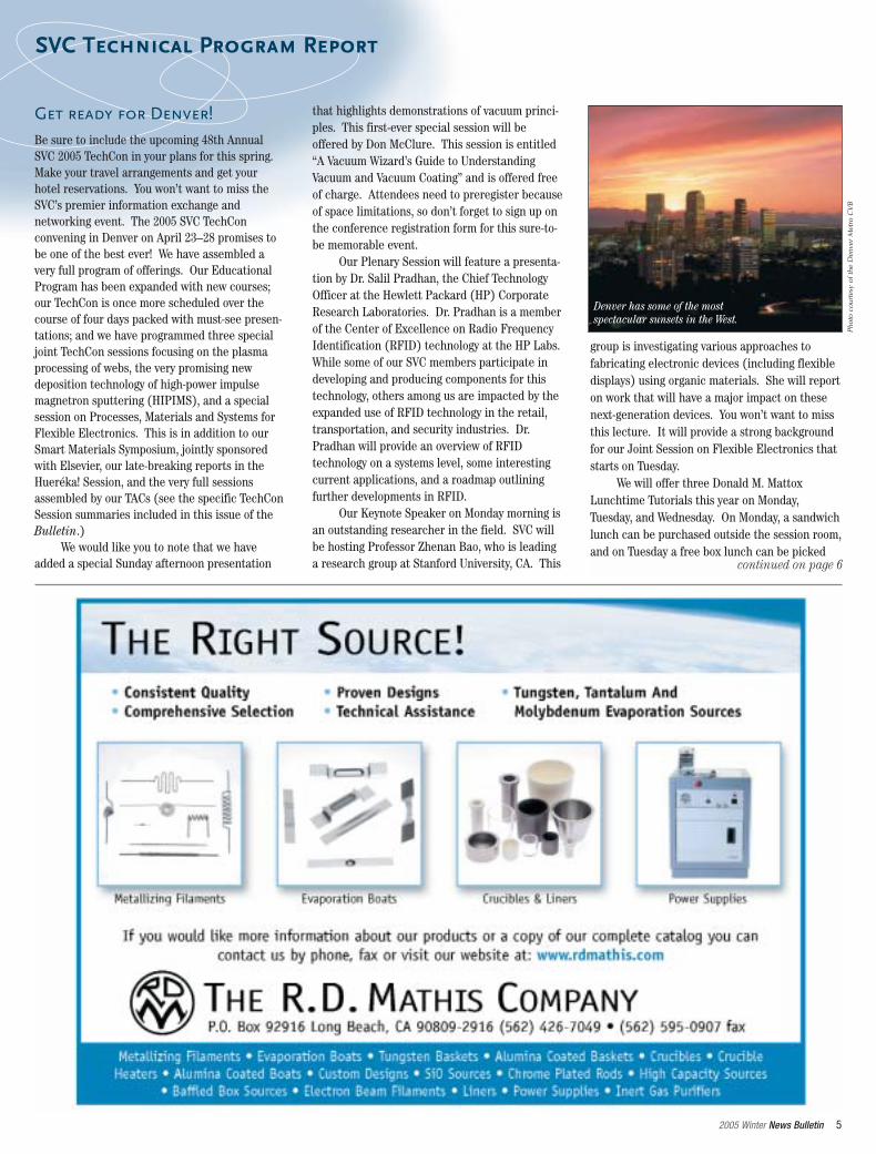
Denver has some of the mostspectacular sunsets in the West.
Phot
o co
urte
sy o
f the
Den
ver
Met
ro C
VB
6 2004 Fall News Bulletin
up in the Exhibit Hall. However, please note, onWednesday that attendees will need to supplytheir own lunch. The topics for our threetutorials will be:
• Monday, April 25th, “Plasma SurfaceEngineering for NanotechnologyApplications,” presented by RalfFellenberg.
• Tuesday, April 26th, “Optical Coatings in
Systems,” presented by H. Angus Macleod• Wednesday, April 27th, “A Guide to
Starting Up a Technology-BasedBusiness,” presented by John B. Fenn, Jr.
Monday evening we will once again conveneour Hueréka! Session to capture late-breaking keypresentations. This is a popular session, so youwon’t want to miss it. The popular TechnologyForum Breakfasts are back on Tuesday andWednesday, and the “Meet the Experts” Cornerwill convene on Monday, Tuesday, and Wednesdayto assist attendees who have special processingproblems or basic questions.
Tuesday evening we will hold a special SVC
workshop covering “The Past, Present, andFuture of the Specialty Roll Coating Industry.”Our organizers will be John B. Fenn, Jr., andRoger Philips who each have an extensivebackground in this area and will host a discus-sion on this timely topic.
Our Smart Materials Symposium will againconvene on Wednesday and will provide furtherdiscussions of systems that change in response totheir environment.
We have a full cadre of exhibitors signed upagain, and the Exhibit Hall will be filled with keyvacuum processing equipment and supporttechnologies.
As we go to press there is still a chance foryou to participate in one of the SVC presentationforums: Hueréka!, our Innovators Showcase, andthe Poster Session venues. However, if you doelect to participate, we will need you to submitan abstract via the SVC Web Site no later thanFebruary 15, 2005.
Our TACs have worked hard to developanother strong TechCon Program. I am sure asyou read their session summaries in this Bulletinyou will come to the conclusion that you need tomake the time to be at SVC this spring.
Please check the SVC Web Site (www.svc.org)for further updates. See you in Denver!
Ric Shimshock, MLD Technologies LLC([email protected]), and Ludvik Martinu,École Polytechnique, Montreal, Canada,([email protected]), are the 2005 SVC ProgramChairs.
SVC Technical Program Reportcontinued from page 5
Exhbitors: Show Your Stuff in the Innovators Showcase
As an exhibitor, you can enhance your presence at the TechConby presenting in the Innovators Showcase, the ideal venue tointroduce new ideas, processes, products, and services to afocused and sophisticated worldwide audience. This approach isparticularly effective when the presentation dovetails with yourcompany’s participation in the SVC Exhibit. Presentations canbe made on any topic related to the vacuum industry and will belimited to 10 minutes (including questions).
Payment of a registration fee to make a presentation in theInnovators Showcase in 2005 is waived. Abstracts must be received before February 15, 2005in order to be included in the Final Program.
Abstract submission guidelines are available at www.svc.org, or contact the SVC at 505/856-7188 or E-mail: [email protected]. There is always keen competition for the presentationslots, and a last-minute submission may lead to disappointment. Submit your abstract forthe 2005 SVC TechCon today!
Phot
o by
Jow
dy P
hoto
grap
hy
Emerging Technologies
The SVC Emerging Technologies program willhave two sessions. The Monday afternoon
session will begin with an invited presentation byDavid Glocker, Isoflux Incorporated, on“Nanocomposite Mo-Ti-N coatings for Wear-Resistant Applications” deposited both by co-sputtering and by sputtering from compositetargets. A dispersoid hardening model was usedto predict the hardness as a function of particlesize and volume fraction of TiN. The next presen-tation will report on multilayer deposition ofrefractory and fusible metals and alloys onpowder materials. Experimental results andimplementation of powder material coatingtechnology is described. This work will befollowed by a presentation of pulsed reactivemagnetron sputtering of photocatalytic TiO2films. Time-resolved optical emissionspectroscopy is used to analyze the pulsedplasma properties during deposition. Thefollowing contribution will discuss surfacecharacteristics of biocompatible hexamethyldis-iloxane-based coatings incorporated with TiO2synthesized in a radio-frequency reactor fromhexamethyldisiloxane and Ti-isopropoxide withaddition of oxygen. Growth mechanisms of TiNand nanocomposite coatings, crystalline TiN inamorphous matrix of Si3N4 and TiCN inamorphous SiCN will be presented next.Nanocomposite materials were synthesized byPECVD from TiCl4/CH4/SiH4/N2 gas mixtures.
The session will proceed with a presentation onlow outgassing silicon-based coatings onstainless-steel surfaces for vacuum applications.The coatings are resilient, inert, and capable ofwithstanding temperatures above 400°C. Thelast presentation in the Monday session willpresent a new ion beam system, where the anodevoltage has a half-wave sinusoidal form. The iongun has been designed to enhance the gasdelivery and anode cooling.
On Tuesday afternoon, the session will openwith a presentation on nanoparticle impregna-tion and deposition of catalytic and diffusionbarrier materials. Impregnation of metal foamsamples exhibiting a uniform coating coveragewill be described. The following presentationwill discuss PVD of films on ferromagneticsubstrates in magnetized plasma systems. PVDregimes in high-density plasma must be adapted,
2005 Winter News Bulletin 7
continued on page 8
Win a $200 Cash Award for the Best Poster!
At last year’s TechCon in Dallas, the SVC awarded$200 for the Best Poster presentation and partici-pants displayed more than a dozen posters on amyriad of vacuum related topics.
Once again, the Program Committee welcomesposter presentations on subjects of technicalinterest for inclusion in the Best Poster Contest atthe 2005 TechCon. Abstracts must be submittedusing the On-line Abstract Submission process at www.svc.org. A manuscript is requiredfor review at the TechCon for the entry to be eligible to receive the award and to bepublished in the Conference Proceedings.
Each presenter will be provided one side of an 8 ft. by 4 ft. poster board for display of textand graphics describing the work. Poster presenters will arrange their display on Mondaymorning, April 25, and will be required to be available at their posters to answer questionsfrom 4:30 p.m. until 7:00 p.m. that same day.
The Poster Session is an excellent way to present your work in a relaxed question andanswer format. Submit your abstract today!
Phot
o by
Jow
dy P
hoto
grap
hy
8 2004 Fall News Bulletin
taking into account the effect of, for example,martensitic steel on bombardment by energeticparticles. The session will proceed with anintroduction of space-based deposition technolo-gies for solar power and astronomical applica-tions. The last presentation is devoted toatmospheric pressure plasma and its applica-tions. An atmospheric pressure plasma jet can beused in a downstream or remote regime forsurface cleaning, etching, activation, and reactivedeposition and plasma polymerization.
Join us to hear about new topics, technolog-ical solutions, and emerging processes in coatingand surface treatment.
Hana Baránková, Uppsala University, Sweden([email protected]), and Lad Bárdos,Uppsala University, Sweden([email protected]), are the EmergingTechnologies TAC Co-Chairs.
Joint Session on theProcesses, Materials, andSystems for FlexibleElectronics and Optics
This Joint Session is devoted to hot topics ofprimary interest to the SVC community. In
2005, this session, jointly organized by the SVC
Vacuum Web, Optical Coating, Large Area, andPlasma Processing TACs will focus on recentadvances in the area of “Flexible Electronics andOptics,” stimulated by the technological andeconomic challenges in the fields of displays,security devices, and energy control.
The 2005 program will feature this JointSession on Tuesday morning. Experts from sixdifferent countries and two continents will sharewith us the results of their latest work on thefabrication processes, materials aspects, and filmperformance in conjunction with their applica-tions on flexible polymeric substrates. Roger W.Phillips, Flex Products – a JDSU Company, willintroduce the session with an invited talk entitled“Using Vacuum Roll Coaters to Produce Anti-Counterfeiting Devices.” This presentation willbe followed by a series of original presentationsdevoted to phase-modulated spectroscopicellipsometry for OLEDs, PECVD silicon carbidecoatings for organic luminescent devices,multilayer ultra barrier coatings, Al2O3 barriercoatings by atomic layer deposition (ALD), ion-controlled performance of transparent conductiveoxides, TiO2 for filters in plasma displays, andpermeability testing.
Closely related to the topic of this jointsession is the Tuesday afternoon Workshop on“The Past, Present, and Future of the SpecialtyRoll Coating Industry” moderated by Roger W.Phillips and John B. Fenn, Jr.
We look forward to a very stimulatingsession, and encourage you to bring suggestions
SVC Technical Program Reportcontinued from page 7
Vacuum Research Limited • 2419 Smallman Street • Pittsburgh, PA 15222 USA(800) 426-9340 • (412) 261-7630 • FAX (412) 261-7220 • [email protected]
Throttlemaster is a registered trademark of Vacuum Research.
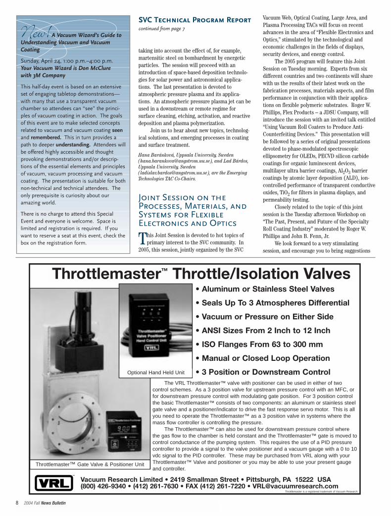
Throttlemaster™ Gate Valve & Positioner Unit
Optional Hand Held Unit
• Aluminum or Stainless Steel Valves
• Seals Up To 3 Atmospheres Differential
• Vacuum or Pressure on Either Side
• ANSI Sizes From 2 Inch to 12 Inch
• ISO Flanges From 63 to 300 mm
• Manual or Closed Loop Operation
• 3 Position or Downstream ControlThe VRL Throttlemaster™ valve with positioner can be used in either of two
control schemes. As a 3 position valve for upstream pressure control with an MFC, orfor downstream pressure control with modulating gate position. For 3 position controlthe basic Throttlemaster™ consists of two components: an aluminum or stainless steelgate valve and a positioner/indicator to drive the fast response servo motor. This is allyou need to operate the Throttlemaster™ as a 3 position valve in systems where themass flow controller is controlling the pressure.
The Throttlemaster™ can also be used for downstream pressure control wherethe gas flow to the chamber is held constant and the Throttlemaster™ gate is moved tocontrol conductance of the pumping system. This requires the use of a PID pressurecontroller to provide a signal to the valve positioner and a vacuum gauge with a 0 to 10vdc signal to the PID controller. These may be purchased from VRL along with yourThrottlemaster™ Valve and positioner or you may be able to use your present gaugeand controller.
Throttlemaster™ Throttle/Isolation Valves
™
New! A Vacuum Wizard’s Guide toUnderstanding Vacuum and VacuumCoating
Sunday, April 24, 1:00 p.m.–4:00 p.m.Your Vacuum Wizard is Don McClurewith 3M Company
This half-day event is based on an extensiveset of engaging tabletop demonstrations—with many that use a transparent vacuumchamber so attendees can “see” the princi-ples of vacuum coating in action. The goalsof this event are to make selected conceptsrelated to vacuum and vacuum coating seenand remembered. This in turn provides apath to deeper understanding. Attendees willbe offered highly accessible and thoughtprovoking demonstrations and/or descrip-tions of the essential elements and principlesof vacuum, vacuum processing and vacuumcoating. The presentation is suitable for bothnon-technical and technical attendees. Theonly prerequisite is curiosity about ouramazing world.
There is no charge to attend this SpecialEvent and everyone is welcome. Space islimited and registration is required. If youwant to reserve a seat at this event, check thebox on the registration form.
and ideas for similar future activities.
Ludvik Martinu, École Polytechnique, Montreal,Canada ([email protected]), Optical Coating TACChair, Peter J. Moulds, Ursa International Corporation([email protected]), Vacuum Web Coating TACCo-Chair, Michael Andreasen, VACUUM COATINGTechnologies, Inc. ([email protected]),Large Area Coating TAC Chair, and VasgenShamamian, Dow Corning Corporation([email protected]), Plasma ProcessingTAC Chair, jointly organized this session
Joint Session on PlasmaProcessing of Webs
The Plasma Processing and Vacuum Web TACsare delighted with the enthusiastic turnout of
our solicitation for a joint session specificallydevoted to the science and technology associatedwith the plasma processing of flexible substrates.Plasma processing of flexible webs has becomeincreasingly important in both the commercializa-tion of new products and the reduction of costsfor production of established products. Plasma-based technologies offer potentially higherdeposition rates and a more flexible choice inboth gas phase and surface depositionchemistries. Many researchers now considerplasma-based technologies to be an enabling andeconomically desirable technology in polymer-based web coating. However, there are manytechnical issues to be resolved before themarriage of the two communities is solidified.
This year our invited speaker, Moses David ofthe 3M Corporation, will discuss continuousplasma-enhanced chemical vapor deposition(PECVD) of diamond-like carbon (DLC) films onmoving substrates. The session will host anumber of talks that present the plasma andsurface chemistry pretreatment for the promotionof adhesion and functionalization of chemicalstructures to polymer webs. Several talks willalso feature the development of new atmosphericdischarges that introduce specific surfacechemical structures that exhibit hydrophilic andhydrophobic behavior. Some of these novelsources employ liquid precursors, which openopportunities to perform very exciting plasmachemistry and novel thin film applications.Finally, detailed studies of barrier films and theirperformance with polymer surface and bulk fillersand agents will be presented.
We encourage you to attend and learn aboutthe latest innovations in plasma-based webcoating and converting!
Vasgen Shamamian, Dow Corning Corporation([email protected]), is the PlasmaProcessing TAC Chair, and Peter Moulds, UrsaInternational ([email protected]), is the VacuumWeb Coating TAC Co-Chair.
Large Area Coating
The SVC Large Area Coating TAC will sponsortwo sessions of presentations this year. The
first session will start off with an invited papergiven by Dr. Takuji Oyama of Asahi Glass CompanyLtd., titled, “Theoretical Considerations of
Magnetron Discharges with Respect to Arcing andPlasma Structure in DC and AC Sputtering,” inwhich he proposes a three-step model for betterunderstanding of cathode arcing phenomena.Also covered will be co-author Dr. Shidoji’s workin simulation of the plasma structures ofunbalanced and bipolar magnetrons.
Following the opening invited talk will be amini session on sputter technology in which newand advanced hardware, processes, applications,and systems are presented in the followingpresentations:
• “Monte Carlo Simulation of AnomalousErosion in Large Area SputterMagnetrons,” presented by Guy Buyle ofGhent University
• “Flexibility and ProductivityImprovements in a New Coating SystemDesign,” presented by Philip Greene ofVACUUM COATING Technologies
• “Advanced Rotatable Magnetron ModuleDesigned for Large Area Glass Coaters,”presented by Joern Brueckner of VONARDENNE
• “Advances in Sputter Hardware forRotating Cylindrical MagnetronSputtering,” presented by Krist Dellaert ofBekaert Advanced Coatings
• “Large Area Rotating CylindricalMagnetron Sputtering: Magnetic SystemEnhancements,” presented by AnjaBlondeel of Bekaert Advanced Coatings
• “MF and RF Systems for Large Area GlassCoating and Flat Panel DisplayApplications,” presented by ThomasRettich of Huettinger Elektronik
• “New Steps Toward Large Area Plasma-Activated EB PVD,” presented byEkkehart Reinhold of VON ARDENNE
• “About the Application of Ultra-Hydrophilic Coatings to High VoltageTransmission Lines,” presented byClaudia Roero of the Swiss FederalInstitute of Technology
The second session will start off with aninvited talk presented by Professor Roger deGryse entitled, “Aspects of Target VoltageBehavior in Reactive Sputtering,” in which Dr. deGryse discusses his research into target poisoningrelative to two predominant mechanisms:subplantation of reactive gas ions beneath thetarget surface and chemisorption on the targetsurface. He will discuss how these twomechanisms have a significantly differentinfluence on target voltage and surface poisoning.Following the opening invited talk will be a minisession on the latest developments in sputtertarget manufacturing and presentations onmodeling plasma impedance, use of pulsedplasmas in the reactive deposition of ITO, use ofion sources in large area coating processes, andthe influence of deposition parameters onsputtered chromium morphology in presentationsentitled:
• “Modeling of the Plasma Impedance in
2005 Winter News Bulletin 9
continued on page 10
SVC Technical Program Reportcontinued from page 9
10 2005 Winter News Bulletin
Reactive Magnetron Sputtering for Various Target Materials,” presentedby Andreas Pflug of the Fraunhofer Institute for Surface Engineering andThin Films IST
• “Hydrogen Doping of ZnO:Al Films Deposited by Pulsed-DC Sputtering ofCeramic Targets,” presented by Florian Ruske of the Fraunhofer Institutfur Schicht und Oberflachentechnik (IST)
• “New Developments in the Manufacturing of Thermal Sprayed CylindricalTargets,” presented by Hilde Delrue of Bekaert Advanced Coatings
• “Pulsed Plasmas for Reactive Deposition of ITO Layers,” presented byWolf-Michael Gnehr of the Fraunhofer Institut FEP
• “Closed Drift Ion Sources for Large Area Architectural Glass Coating,”presented by Denis M. Shaw of Advanced Energy Industries, Inc.
• “Application of HIP (Hot Isostatic Pressing) to Rotatable SputterTargets,” presented by Alan Plaisted of Soleras Ltd.
• “Flowformed Rotatable Sputtering Targets,” presented by MatthewFonte of Dynamic Machine Works, Inc.
• “Influence of Deposition Parameters on the Morphology of SputteredChromium Coatings,” presented by Fang Yee of Benet Laboratories
All in all, it looks like we will have two interesting and informative sessionscovering the latest developments in systems, hardware, modeling, targets, andapplications in the large area coating arena for 2005.
Michael Andreasen, VACUUM COATING Technologies, Inc. ([email protected]),is the Large Area Coating TAC Chair, and Johannes Strümpfel, VON ARDENNEAnlagentechnik GmbH ([email protected]), is the Assistant TAC Chair.
Optical Coating
The 2005 SVC Optical Coating technical program has attracted a largenumber of presentations. Important developments in this field and the most
recent trends are characterized by the diversification of activities andillustrated by a large spectrum of topics. The program will consist of presenta-tions divided into two morning sessions and one afternoon session; in addition,selected talks will be presented as part of the joint session focused on flexibleoptics and electronics.
The first optical coating session on Monday morning will highlight a veryimportant subject within the optical coating community, namely, the “AdvancedOptical Metrology and Measurement Accuracy.” This topic will be introduced bythe invited talk of D.E. Aspnes, North Carolina State University, entitled,“Recent Advances in Optical Characterization of Thin Films by SpectroscopicEllipsometry.” Subsequent speakers will discuss specific examples of filmanalysis by ellipsometry in the context of solar selective coatings, modelling ofanisotropic stacks, and in situ real-time film growth monitoring. This topic willbe further elaborated by the analysis of sensitivity variation during manufactureand statistical process analysis for reverse engineering.
The second optical coating session on Wednesday afternoon on “NewOptical Materials and Processes” will be introduced by Peter Mascher from theMcMaster University in Hamilton, Canada, who will focus on “Modelling andExperimental Determination of the Optical Properties of Thin Films.”Contributed presentations in this session will discuss different complementaryaspects, in particular, new and novel deposition approaches (end-Hall ion sourceand closed field magnetron sputtering), materials synthesis, and characteriza-tion and optimization for enhanced performance (wear-resistant coatings onplastics, high-index niobium and scandium oxide films, fluoride films, super-smooth surfaces, interface layers for next-generation DVD, and plasmonresonance characteristics for biosensors).
The third session on Thursday morning will be devoted to “AdvancedApplications of Optical Coatings,” providing a unique set of examples illustratingrecent trends in this area. The opening presentation in this session will be byJoanne Jones-Meehan from the Naval Research Laboratory in Washington, D.C.Her talk, entitled, “Rapid Optical Immunoassays to Detect EnvironmentalAgents and Pathogens in Clinical Specimens,” will introduce the fast-evolvingfield of biomedical applications. Other specific examples will include thin film
Reliability • Stability • Flexibility
11 Kondelin Road Gloucester, MA 01930Phone: 978-282-0620
For a copy of our new product catalog, visit our website: www.comdel.com
or email us at: [email protected]
High power plus exceptional
reliability and stability.
Improve the performance of your processwith the RELIABILITY and STABILITY ofComdel's RF power supplies. Our ruggedCXH Series high power supplies combinetime-tested power device designs, precise
and repeatable power control with a solid-state driverthat does not require tuning or adjustments. For the highpower demands of plasma, flat panel display, thin filmprocesses and a wide range of industrial heating applications, the CXH Series delivers:
• Reliability and stability in the presence of erratic loads• Fixed frequency operation from
2 to 40 MHz• Standard power ranges: 15kW,
25kW, 50kW• Precise power management
and diagnostic monitoring
Find the perfect fitfor your process!
2005 Winter News Bulletin 11
security devices, coatings for extreme ultraviolet (EUV) applications, nonpolar-izing beam splitters, and process optimization involving rate and uniformitycontrol and stress reduction. This session will also feature a student presenta-tion from Ècole Polytechnique in Montreal, entitled, “Playing with Light: TheQuest for New Optically Variable Devices.”
An integral part of the Optical Coating activities is a series of traditionaltechnology forum breakfasts. Apart from the gastronomic pleasures, thesesessions encourage discussion. Conversation on “Optical Monitoring and ProcessControl” will be facilitated by Ric Shimshock, MLD Technologies, on Tuesdaymorning. Discussions of “N- and P-type Transparent Conductive Coatings,” facili-tated by Clark Bright, 3M Company, and “Ion- and Plasma-Based Processing forOptical Coatings,” facilitated by Ludvik Martinu, École Polytechnique, will takeplace on Wednesday morning. H. Angus Macleod, Thin Film Center, Inc., willshare his wisdom with us in his lunchtime tutorial lecture on real-life experiencewith “Optical Coatings in Systems” on Tuesday at 12:40 p.m.
We expect a very exciting and stimulating program and look forward to asuccessful conference.
Ludvik Martinu, École Polytechnique, Montreal ([email protected]), is the 2005Optical Coating TAC Chair, and George Dobrowolski, retired from the National ResearchCouncil of Canada, Ottawa ([email protected]), is the 2005 Optical CoatingAssistant TAC Chair.
Plasma Processing
Plasma processing is as dynamic as ever, with new plasma sources,techniques, and applications that will revolutionize the manufacturing thin
film technology base in the future. In order to stay current with the rapidchanges in our community, the SVC Plasma Processing TAC has assembled aprogram filled with the latest developments from corporate, government, andacademic laboratories around the world.
This year, we have a special session within our TAC forum to address thegrowing technique known as high-power impulse magnetron sputtering(HIPIMS). HIPIMS has found its first applications in hard coatings, substratepretreatment, low-friction coatings, and optical layers. The high ionization ofthe HIPIMS plasma provides opportunities to develop novel and improvedmaterials with unique microstructure and macroscopic properties. HIPIMSprocessing requires a fundamental understanding of the dynamics in theplasma, on the target, and the substrate surface, as well as strong developmentof the hardware. Professor Ulf Helmersson of Linköping University, Sweden, willgive us an overview of the science of the technique, opportunities, applications,and limitations. We will see plasma diagnostic presentations and severalapplications for coating technology. Come learn what all the buzz is about!
Finally, our regular two sessions will cover the broad area of plasmascience as it pertains to thin film deposition. Paul Gagnon of Corning, Inc., willdiscuss a variety of plasma sources and how they are employed to tailor thesurface chemistry of polymers to medical drug discovery applications. ProfessorJurgen Engemann of JE Plasma Consult will show spatially and temporallyresolved optical emission studies of the development of plasma “bullets” in anatmospheric plasma jet and its consequence on dissociation chemistry inmolecular gases. The contributed presentations span broad topics in sourcesfrom electron-beam-generated plasmas, barrier discharges, pulsed systems,radio frequency, and microwave sources. Plasma diagnostics, plasma theory andmodeling, and process chemistry for both PECVD and PVD will be included aswell. Diagnostic techniques for experiments such as sampling mass spectrom-etry and optical emission are featured. The talks and question/answer periodprovide an excellent opportunity to learn from the experts presenting theirwork. If you have any questions, please contact the TAC Chairs.
The Plasma TAC breakfast is scheduled for Monday morning at 7:00 a.m.Please contact one of the TAC chairs if you are interested in attending.
Vasgen Shamamian, Dow Corning Corporation ([email protected]), isthe Plasma Processing TAC Chair, and Scott Walton, Naval Research Laboratory([email protected]), and Falk Milde, VON ARDENNE Anlagentechnik GmbH([email protected]), are the Assistant TAC Chairs.
continued on page 12
12 2005 Winter News Bulletin
Process Control andInstrumentation
The SVC Process Control & Instrumentationsession remains focused on the instrumen-
tation and control techniques used in vacuumcoating processes. Innovations and develop-ments used to create new coatings or thatimprove quality, productivity, or reduce cost areof special interest.
The 2005 Process Control &Instrumentation session will begin with aninvited presentation, “Multi-Gas, Multi-Zone
Reactive Sputtering Control System,” from BillSproul, Advanced Energy Industries. Theoperation of a control system capable of control-ling up to three reactive gases in as many as 15zones with unique feedback signals will bediscussed. A topically related presentation,“Long-Term Process Control and Stability inReactive Sputtering,” will follow, exploring thebenefits of multi-sensor and smoothed datafeedback to prevent process drift or distur-bances. Diverse presentations on “Pole PieceInsertion in Target for NiCr MagnetronSputtering: Influence on Plasma and CoatingProperties,” “Coating of Powder Particles in aMagnetron Plasma,” “Spectroscopic MuellerMatrix Polarimeter Using Liquid Crystal DevicePolarization State Generator and Detector,” “On
SVC Technical Program Reportcontinued from page 11
the Application of Quantum Cascade Laser-Absorption Spectroscopy for Plasma ProcessMonitoring,” “True 2-D Imaging Spectroscopy in aReactive Sputter Process for Large-Scale OpticalGlass Coating,” and “An Optical Sensor for Real-TimeIn-Situ Endpoint Monitoring During Dry Etching ofIII/V Multi-Stack Layers,” will follow. And finally, thesession will close with two presentations on arcmanagement: “Arc Handling Considerations for DCSputtering Power Supplies” and “Managing Arcs inRF-Powered Plasma Processes.”
Please plan to join us and learn more aboutthese very exciting and relevant topics to the vacuumcoating process.
J. Grant Armstrong, Carberry Technologies([email protected]), and David Chamberlain,MKS Instruments, Inc.([email protected]), are the ProcessControl and Instrumentation TAC Co-Chairs.
Smart Materials Symposium
This symposium focuses on new and emergingfunctional materials and coatings with unique
intelligent properties as indicators, protectivecoatings, early warning of tampering, aging, biolog-ical and chemical change. The intent of theSymposium is to bring together many specialistsworking on active and intelligent materials. Smartmaterials is a growing area for new products.Examples of smart materials are smart switchableglass and plastic for use in visors, architectural andautomotive glazing. These coatings can be used fordynamic energy and light control. Some technologiescan switch in the infrared wavelengths. Othermaterials include switchable polymers, smart ink anddynamic labeling. Also, included in this group arehighly refined evacuated glazing, which can be usedfor both energy and acoustical control. Otherdeveloping areas concern health applications such asdrug delivery systems from multilayer patches andfood safety packaging. This mixture of technologywill broaden the future of coating technology.
See page 15 for a sneak preview article onLarge-Scale Organic Photovoltaics, to be presentedon Wednesday, April 27, as part of the SmartMaterials Symposium in Denver.
Carl Lampert, Star Science ([email protected]), is theSmart Materials Symposium Organizer.
Tribological & DecorativeCoating
The Tribological & Decorative Coating session of theSVC 2005 TechCon has attracted a number of very
interesting presentations on topics in this field.Presentations will deal with a wide spectrum of topicsin the field, ranging from fundamental analysisthrough developments of new technologies, industrialapplication developments, and decorative coatingdevelopments and applications.
In the group of sessions on the fundamentalanalysis of coating systems, a very interesting invitedpresentation has been submitted dealing withsuperhard nanostructured T-B-C-Al-N films developedwith closed-field unbalanced magnetron by the
2005 Winter News Bulletin 13
Colorado School of Mines. The presentation byJohn Moore will reveal the results of a systematicinvestigation into the relationship betweenmicrostructure and mechanical properties of thesecoating systems consisting of a mixture of differentnanoparticles in an amorphous BN-matrix.
Two presentations from the University ofGroningen, The Netherlands, will be contributedon the topic of carbon-based coatings of lowfriction combined with good wear behavior. Thepresentation of Y. Pei will deal with analysis ofnanostructured T-C coatings. These coatings havebeen investigated in different environments(humidity, lubricant, temperature). The structurewill be related to results of detailed examinationsof the mechanical film properties. Nuno Carvalhowill address the relationship between structureand properties of tungsten-based metal-DLC filmsproduced with different process parameters,including sputtering from tungsten versustungsten carbide targets. Guido Janssen from theTechnical University in Delft will present theresults of investigations on the tensile andcompressive stress in hard coatings. Conclusionsof theoretical and empirical results of investiga-tion will show the existence of a gradient in stressfrom tensile at the interface to compressive at thesurface of the coating.
Representatives of the two major job coatersworldwide will make presentations from theperspective of industrial automotive componentsand applications. André Hieke from IonBond willpresent an interesting comparison between the
mechanical properties of DLC coatings producedwith RF and DLC coatings and produced withmid-frequency PACVD. Markus Esselbach ofBalzers will talk about component coatings for theautomotive industry produced with a new type ofhigh-volume coating machine that enables theproduction of coatings with competitive prices.Coatings for machining applications will beaddressed by Papken Hovsepian of SheffieldHallam University. This talk will present a newsuperlattice structured TiAlN/VN PVD coating as anew potential coating for machining of Al and Tialloys for aerospace and automotive components.He will show that the combination of low frictionand hardness of the coating yields excellentresults in cutting of the aforementioned highlyabrasive and adhering materials.
New technologies in the form of hybridprocesses, especially processes where surfacenitriding and coating are combined, are a thirdgroup of presentations. J.-D. Kamminga of theNetherlands Institute for Metals Research isinvited to present developments achieved on theproperties of a CrN coating supported by anitrided base layer. Both the nitrided layer andthe PVD-coating are produced in a combinedprocess in one PVD-machine without interruptionof the vacuum. Kamminga will show that it ispossible to improve mechanical properties of thecoated system substantially by the preceding in-situ nitriding step. Jaime Trujillo of theUniversidad del Valle in Cali, Colombia, a student
This exciting TechCon session enables authors to present their
late- breaking results, developments, disclosures, and stimulating
achievements, long after the official abstract submittal deadline has passed.
It will be run independently of all other TechCon sessions on Monday
evening. The criteria for Heuréka! presentations are as follows:
• 20-minute presentation. Allow about five minutes for questions.
• The presentation abstract must be submitted (submit on-line at www.svc.org) no later than February 15, 2005, to be included in the Final Program.
• A manuscript is required for the Conference Proceedings.
This is not a “catch-all” session for late papers, and the number ofpresentations will be limited. Last year, this popular session allowed formany presentations that would not have been possible otherwise. Onceagain, Heuréka! will be SVC’s forum for new and exciting “hot-off-the-press” developments. If you have questions about this session, E-mailLadislav Bárdos at [email protected] or Hana Baránková [email protected]
Heuréka! Abstract Deadline: February 15, 2005Submit your 200-Word Abstract On-line at www.svc.orgto be included in the Final Program.
Heuréka!Post-DeadlineRecentDevelopmentsSession at the2005 TechConExpected to beStanding-RoomOnly Again!
Date and Time:Monday, April 257:15 p.m.–9:15 p.m.
Moderators:L. Bárdos and H.Baránková, UppsalaUniversity, Sweden
Heuréka!Post-DeadlineRecentDevelopmentsSession at the2005 TechConExpected to beStanding-RoomOnly Again!
Date and Time:Monday, April 257:15 p.m.–9:15 p.m.
Moderators:L. Bárdos and H.Baránková, UppsalaUniversity, Sweden
continued on page 14
Workshopon Specialty Coatings
“The Past, Present, and Future of theSpecialty Roll Coating Industry”
Tuesday, April 26, 5:30 p.m. –6:30 p.m.Workshop Organizers: Roger Phillips, FlexProducts, Inc. and John B. Fenn, Jr., Fennagain
Bring Your Questions! This should be alively experience.
Vacuum roll-to-roll coating has been aroundfor over half a century. In fact, one of its firstcommercial applications was a specialty rollcoating process used to deposit very thinfilms of gold for decorative processes in 1934.In the late 1970’s and early 1980’s companiesbegan to apply other vacuum coatingtechniques such as sputtering, PECVD andPolymer Multi-Layer (PML) techniques todevelop specially engineered thin filmcoatings to do highly specific and technicallydifficult jobs. Out of that work cametransparent conductive coatings for use intouch panels, displays and shielding.
Current concerns question the health of thebusiness and where is it heading? Thisworkshop will attempt to address theseissues and try to remove some of the cloudsfrom the future’s crystal ball.
14 2005 Winter News Bulletin
sponsored by the SVC Student SponsorshipProgram, will give a presentation on the effects ofduplex treatment (nitriding and PVD coating),where the nitriding step preceding the actualcoating step is either a plasma nitriding or saltbath nitriding step. Several coatings will beinvestigated in this presentation, all preceded bya nitriding step.
In the field of decorative coatings, aninvited contribution by Michiel Eerden fromHauzer and Papken Hovsepian of SheffieldHallam University will be presented by PapkenHovsepian. This presentation will provide anoverview of the developments of the last decadeon applications of PVD in the decorative field, aswell as an overview on the specialized develop-ment work of Sheffield Hallam University in thelast decade on corrosion protection and on newcolors and applications by anodizing of coatings.Pedro Carvalho of the University of Minho,Portugal, a second student sponsored by the SVCStudent Sponsorship Program, will present hiswork on the characterization of reactivesputtered decorative zirconium oxynitridecoatings. He will relate the optical measurement
results to structure, mechanical, and electricalcharacterization results. The presentation ofVispi Gheyara of Shiloh Industries will deal withinvestigations into the correlation between aXenon weatherometer and outdoor testing of UVcurable clearcoat PVC samples mounted on avehicle. Michiel Eerden, of Hauzer TechnoCoating BV, will make a presentation on thedecorative properties that depend on thecomposition of the coating. Comparisons aremade for TiCN-coatings produced with arcevaporation processes and those produced withunbalanced magnetron sputtering processes.
Roel Tietema, Hauzer Techno Coating BV, TheNetherlands ([email protected]), is the Tribologicaland Decorative Coating TAC Char, and Gary Doll,Timken Research ([email protected]), is theAssistant TAC Chair.
Vacuum Web CoatingThe Vacuum Web Coating TAC’s annual breakfastcommittee meeting will take place on Mondaymorning, April 25, 2005, at 7:00 a.m. Weencourage all SVC Web TAC committee membersand those interested in joining Web TAC toattend. This meeting is extremely importantbecause it sets the tone for our sessions at the2006 Technical Conference.
For the 48th Annual Technical Conference,
the Web TAC has assembled two sessions and isparticipating in two joint sessions. One jointsession will be Processes, Materials, and Systemsfor Flexible Electronics and Optics to be heldwith the Optical Coating, Large Area Coating,and Plasma Processing TACs. The other jointsession new for 2005, and at the request of theWeb TAC members attending the annualbreakfast committee meeting, will be PlasmaProcessing of Webs, involving both the Web TACand the Plasma Processing TAC.
On Monday morning, we will kick off withthe topic of vacuum web applications andprocesses. Reiner Kukla of Applied Films GmbHwill present the invited talk on “MultiprocessRoll-to-Roll Web Coater: First Results.” Cutting-edge products like flexible displays, flexibleprinted circuits, and flexible solar cells requireproduction web coaters with multiprocesscapacity. Other presentations will include theplasma-enhanced CVD process, limitation of heattransfer mechanisms, gas barrier properties ofSiOx films, and security devices.
On Tuesday afternoon, the Web TAC sessionwill be on vacuum web industrial applications.The invited presentation on “The Development ofGlobal Markets for Vacuum Coated Films andPapers” will be made by William Llewellyn ofAWA Alexander Watson Associates BV. Thispresentation will detail global markets, regionaluses, product volumes, and commercial develop-ment of vacuum-coated films and papers. Thistalk will be a great kick off for the session. Otherpresentations will include discussions of theinfluence of PET substrates, barrier studies ofmultilayer films, copper on polyimide films, anddurability and cost analysis of solar reflectivehard-coated materials.
In addition to the sessions and jointsessions sponsored by WebTAC, Roger Phillipsand John B. Fenn, Jr. have volunteered toorganize a Workshop at the 2005 SVC TechCon onTuesday at 5:30 p.m. on the “Past, Present, andFuture of the Specialty Roll Coating Industry.”Read more about this Workshop on page 13.
Peter J. Moulds, Ursa International Corporation([email protected]), and Charles BishopC.A. Bishop Consulting Ltd.
([email protected]),are the Vacuum Web TAC Co-Chairs.
SVC Technical Program Reportcontinued from page 12
2005 TechCon Plenary Address“RFID Technology, Promise and Challenges” Presented by Salil Pradhan Sunday Evening, April 24, after the Opening Ceremonies at 7:00 p.m.
Radio Frequency Identification (RFID) is a proven technology that has beenaround since the early 1970’s. However, the promise of improved supplychain visibility and management, real time logistics and inventory control inoperations has been limited by the lack of standards, the lack of a system-atic approach and cost. HP Labs has recently established a RFID Center ofExcellence in Palo Alto, CA to implement, characterize and expand RFID
technologies in the marketplace. Hewlett Packard Laboratories (HP Labs) has been a leaderin this field and was an early adopter of RFID technology within its own operations. HP isalso a producer of RFID-enabled goods and a proven innovator in the RFID Field offeringconsulting, technology solutions and enterprise applications. HP RFID technologies arebeing widely implemented in the Wal-Mart supply chain, within the US government and withindustrial concerns such as Hasbro Inc. This talk will review the current RFID landscape,survey the RFID Developmental Roadmap and provide a vision for RFID Technology.
Dr. Salil Pradhan is the Chief Technical Officer for RFID Programs at HP Labs in Palo Alto, CA.
2005 Winter News Bulletin 15
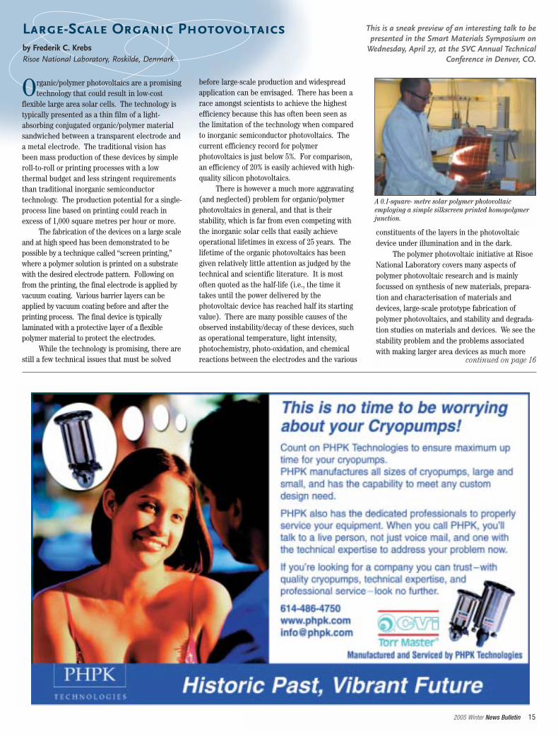
Organic/polymer photovoltaics are a promisingtechnology that could result in low-cost
flexible large area solar cells. The technology istypically presented as a thin film of a light-absorbing conjugated organic/polymer materialsandwiched between a transparent electrode anda metal electrode. The traditional vision hasbeen mass production of these devices by simpleroll-to-roll or printing processes with a lowthermal budget and less stringent requirementsthan traditional inorganic semiconductortechnology. The production potential for a single-process line based on printing could reach inexcess of 1,000 square metres per hour or more.
The fabrication of the devices on a large scaleand at high speed has been demonstrated to bepossible by a technique called “screen printing,”where a polymer solution is printed on a substratewith the desired electrode pattern. Following onfrom the printing, the final electrode is applied byvacuum coating. Various barrier layers can beapplied by vacuum coating before and after theprinting process. The final device is typicallylaminated with a protective layer of a flexiblepolymer material to protect the electrodes.
While the technology is promising, there arestill a few technical issues that must be solved
before large-scale production and widespreadapplication can be envisaged. There has been arace amongst scientists to achieve the highestefficiency because this has often been seen asthe limitation of the technology when comparedto inorganic semiconductor photovoltaics. Thecurrent efficiency record for polymerphotovoltaics is just below 5%. For comparison,an efficiency of 20% is easily achieved with high-quality silicon photovoltaics.
There is however a much more aggravating(and neglected) problem for organic/polymerphotovoltaics in general, and that is theirstability, which is far from even competing withthe inorganic solar cells that easily achieveoperational lifetimes in excess of 25 years. Thelifetime of the organic photovoltaics has beengiven relatively little attention as judged by thetechnical and scientific literature. It is mostoften quoted as the half-life (i.e., the time ittakes until the power delivered by thephotovoltaic device has reached half its startingvalue). There are many possible causes of theobserved instability/decay of these devices, suchas operational temperature, light intensity,photochemistry, photo-oxidation, and chemicalreactions between the electrodes and the various
constituents of the layers in the photovoltaicdevice under illumination and in the dark.
The polymer photovoltaic initiative at RisoeNational Laboratory covers many aspects ofpolymer photovoltaic research and is mainlyfocussed on synthesis of new materials, prepara-tion and characterisation of materials anddevices, large-scale prototype fabrication ofpolymer photovoltaics, and stability and degrada-tion studies on materials and devices. We see thestability problem and the problems associatedwith making larger area devices as much more
Large-Scale Organic Photovoltaicsby Frederik C. KrebsRisoe National Laboratory, Roskilde, Denmark
This is a sneak preview of an interesting talk to bepresented in the Smart Materials Symposium on
Wednesday, April 27, at the SVC Annual TechnicalConference in Denver, CO.
continued on page 16
A 0.1-square- metre solar polymer photovoltaicemploying a simple silkscreen printed homopolymerjunction.
Aluminum Gate Valves DN 160-320 Series 12.1 for vacuum and high vacuum isolation
www.vatvalve.com
SimpleQuick and easy maintenance
CleanLow particle generation
SoftSmooth sealing operation
Swiss HeadquartersTel ++41 81 771 61 [email protected]
VAT FranceTel 01 69 20 69 [email protected]
VAT USATel (781) 935 [email protected]
VAT U.K.Tel 01926 452 [email protected]
VAT JapanTel (045) 333 11 [email protected]
VAT KoreaTel 031 704 68 [email protected]
VAT TaiwanTel 03 516 90 [email protected]
VAT BeneluxTel ++31 (30) [email protected]
VAT GermanyTel (089) 46 50 [email protected]
«Split body» design
16 2005 Winter News Bulletin
pertinent than the problem of attaining a high efficiency. The reason for this isthat the chemistry and physics of stable polymer photovoltaic materials will bevery different from the current state of the art, and the efficiency improvementprocess will have to start all over using the new and stable type of materials.
Using the state-of-the-art, commonly employed efficiencies of 1–2% havebeen obtained at Risoe National Laboratory with active areas of 3 to 4 squarecentimetres. Half-lives of the order of ten, 12-hour days in the ambientatmosphere under full solar illumination have been attained (solar irradiation of1000 W/m2, AM1.5). The current state of the art involves the use of a mixture of asoluble fullerene derivative and polymer. Degradation is also observed under theexclusion of oxygen, albeit a little bit slower. Also, when scaling up the area of thedevices, the problems of good process control and conducting the current out ofthe device without (or with little) loss lowers the efficiency dramatically. Radicalimprovements are thus needed in order to take polymer photovoltaics further andhopefully put this technology to work in society.
The most recent results have been a significant improvement on thelifetime of small area photovoltaic devices. In an oxygen-free environment, testdevices have been run under full solar illumination (1000 W/m2, AM1.5) for 500hours with no decay even at high temperature. The efficiency is low (0.1%), butbecause it is a new type of material with different chemistry and device fabrica-tion methods, this is regarded as promising.
The construction of a polymer photovoltaic process line has been initiatedand will be completed in 2005. It permits the fabrication of 0.1-square- metredevices by employing silkscreen printing and large area vacuum coating withmultiple e-beam and thermal sources. Current results have been obtained withoperation in air, but the final process line will allow for preparation, processing,evaporation, testing, and encapsulating large area devices (0.1 m2) under glove-box conditions.
Large-Scale Organic Photovoltaicscontinued from page 15
2005 Winter News Bulletin 17
Donald M. Mattox LunchtimeTutorial ProgramPick up a lunch and join a tutorial!
Here are three great ways to enhance your skills, increase your knowledge, andposition yourself for professional advancement. The Program Committee ispleased to announce the addition of a Wednesday afternoon tutorial with JohnB. Fenn, Jr., entitled “A Guide to Starting Up a Technology-Based Business,”which is not listed in the Preliminary Program. Read more about the tutorialtopics below and plan to “learn at lunch”.
Plasma Surface Engineering for Nanotechnology ApplicationsMonday Afternoon, April 2512:40 p.m.–1:20 p.m.Presenter: Ralf Fellenberg, VDI Technologiezentrum GmbH, Germany
Nanotechnology is often described as the technology of the future. R&Dand applications in the field of nanotechnology are attracting growing interestworldwide.
Plasma Surface Engineering is one of the valid tools for nanoprocessingand was established to achieve properties based on nanoscale effects for manypossible applications and products. Plasma processes use the potential ofnanoparticles, functional coatings, and surface structures. Nanoparticles areused for paints, lacquers, and in UV-reflecting films. These particles can beincluded in protective coatings for household appliances, spectacle lenses,glazing materials for sanitary applications, or in exterior house paints to preventscratches, tarnishing, smudging or algae growth. Functional coatings fabricatedwith special plasma sources as well as systems allow the production of thin filmsfor engines, windows, or mirrors and other parts in cars. Structured surfacescan be prepared via ultra-precision processing to enhance the efficiency ofmachines and measuring tools. In addition, plasma surface engineering isneeded to prepare surface modifications for biomedical applications and toincrease the biocompatibility of implants.
Therefore, nanotechnology and plasma technology as new technologicaltrends will have a powerful impact on the market of the 21st Century. Comelearn about this technology of the future!
Optical Coatings in SystemsTuesday Afternoon, April 2612:40 p.m.–1:20 p.m.Presenter: H. Angus Macleod, Thin Film Center Inc.
After a coating has been designed, it is eventually manufactured, tested,and then applied in a system. The real conditions under which the coatings arefirst tested and later employed can be, and almost invariably are, ratherdifferent from the ideal conditions under which they have been designed. Forexample, it is rare for a coating to be illuminated solely at normal incidence.The effects are not mysterious (in the sense that they can all be explained andcalculated), but if it is the behavior under ideal conditions that is expected,then they can, on occasion, be surprising (sometimes unpleasantly). Thistutorial will survey and explain some of these effects and will include somepitfalls to be avoided.
New! A Guide to Starting Up a Technology-Based BusinessWednesday Afternoon, April 2712:40 p.m.–1:20 p.m.Presenter: John B. Fenn, Jr., Fennagain
There are many times when a person says, “Why don’t I just start upmy own business?” The presenter has asked this question several times andnever really found the proper answers. However, he has learned manypractical lessons during his career and will share these with the audience.This is by no means meant to be “the gospel” for starting up a new company,but this tutorial will address some every day issues that are important.Hopefully, there will be questions and comments stirred up by thepresentation that will contribute as much information to the audienceas the talk does.
Pfeiffer Vacuum Inc.24 Trafalgar Square · Nashua · NH 03063-1988
Tel. 800-248-8254 · Fax [email protected]
Contact us to find out why Pfeiffer Vacuum should be your
first choice for turbo pumps
www.pfeiffer-vacuum.com
Get the CompetitiveAdvantage
Get the CompetitiveAdvantage
Reliability – Indisputably, the most reliableturbo pump manufacturedSupport – An independent solid companyfueled by a highly motivated Support TeamPerformance – Best choice for all coatingapplications with maximum gas load, lightgas pumping and fast pressure/cycle changes
18 2005 Winter News Bulletin
Don’t miss out on this incredible opportunity to exhibit at the SVCTechCon in Denver, CO, April 25–26, 2005. Recognized as the premier
event by engineers, manufacturers, technologists, and scientists within theinternational vacuum coating industry, the SVC TechCon and Exhibit is awise investment of your marketing dollars. Coupled with the SmartMaterials Symposium, this show will bring new prospects and customers yourway. The show has sold out for the last 10 years, so don’t delay in signing upfor booth space. There are only a few remaining spaces, so reserve now forthe best selection.
In addition to the Exhibit itself, there are numerous other opportunitiesto promote your products and services at the TechCon. Your company canalso participate in the Innovators Showcase. This is an opportunity to makea 10-minute presentation about new products, new equipment, or a new
process. This approach is particularly effective when the presentationdovetails with your company’s participation in the SVC Exhibit. Yourcompany can also sponsor a Refreshment Break, Internet Cafe, Beer Blast,and the Heuréka! Session. All sponsors are widely acknowledged in SVCpublications, including the Final Program, News Bulletin, Web Site, and onsignage at the TechCon.
For more information or to reserve your booth, call the SVCAdministrative Office at 505/856-7188, or e-mail [email protected].
Contact Lisa Robillard, SVC Exhibit Committee Chair, Director ofCorporate Communications, MKS Instruments, Inc., if you have questionsabout the 2005 Exhibit. Lisa can be reached at [email protected] at 978/284-4050.
SVC Equipment Exhibit at the 2005 TechCon in DenverTime is running out to reserve booth space at the 48th Annual SVC TechCon!
Phot
o by
Jow
dy P
hoto
grap
hy Exhibit Hours:Monday, April 25
12:00 p.m.–7:00 p.m.
Tuesday, April 2610:00 a.m.–5:00 p.m.
2005 Winter News Bulletin 19
Exhibiting Companies at the 2005 TechCon(as of January 15, 2005)
This is your chance to see the latest in vacuum coating and relatedequipment and technologies! It’s not too late to join these companies thathave already signed up to exhibit at the 2005 show:
A&N Corporation • Academy Precision Materials • Advanced Energy Industries, Inc. •Advanced Vacuum Company, Inc. • Alcatel Vacuum Products, Inc. • AmbiosTechnology, Inc. • Ametek Process Instruments • Angstrom Engineering, Inc. •Angstrom Sciences, Inc. • Applied Films Corporation • Arcotronics-Aerre Machines •Bekaert VDS n.v. • BOC Edwards • CERAC, Inc. • CeramTec, Ceramaseal Division •Dark Field Technologies, Inc. • Denton Vacuum, LLC • Dexter MagneticTechnologies, Inc. • Duniway Stockroom Corporation • Dynamic Machine Works,Inc. • DynaVac • Eddy Company • Elgar Electronics Corporation • EMD IndustriesInc. • ESK - A Ceradyne Company • Ferrotec (USA) Corporation • Fil-Tech, Inc. •Fischer Technology, Inc. • Fraunhofer FEP • Galileo Vacuum Systems, Inc. • GeneralPlasma Inc. • GENERAL Vacuum Equipment Ltd. • GfE Metalle und MaterialienGmbH • Hauzer Techno Coating bv • Helix Technology Corporation • HeraeusIncorporated • HORIBA Jobin Yvon, Inc. • HORIBA-STEC, Inc. • HuettingerElectronic, Inc. • HVA, LLC. • IFU Diagnostic Systems GmbH • IGC - PolycoldSystems, Inc. • INFICON • Inland Vacuum Industries, Inc. • INP Greifswald •Insulator Seal, Inc. • Ionic Fusion Corporation • iplas-innovative plasma systemsGmbH • ISRA Vision Systems Inc. • J.A. Woollam Co., Inc. • KLA-TencorCorporation • k-Space Associates, Inc. • Korea Vac-Tec Co., Ltd. • Kurt J. LeskerCompany • Leybold Optics GmbH • Lubtec Corporation • M. Theiss Hard-andSoftware • Maxtek, Inc. • MDC Vacuum Products Corporation • Midwest TungstenService, Inc. • Mill Lane Engineering Co., Inc. • MKS Instruments, Inc. • NAGYInstruments GmbH • Nor-Cal Products, Inc. • Optilayer, Ltd. • Pfeiffer Vacuum •Phelps Electronics, Inc. • PHPK Technologies, Inc. • Plasma Process Group, Inc. •Plasma Surface Engineering Corporation • Plasmaterials, Inc. • Precision MetalWorks Ltd. • Precision Plus Vacuum Parts, Inc. • Process Materials, Inc. • PVTPlasma und Vakuum Technik GmbH • R.D. Mathis Company • Restek Corporation •Ricor Cryogenic & Vacuum Systems • Rigaku/MSC Vacuum Products • Rocky BrookAssociates, Inc. • Rohwedder, Inc. • SAGE industrial sales, inc. • Saint-GobainCeramics • Semicore Equipment, Inc. • Seren IPS Inc. • SHI - APD Cryogenics, Inc. •
Sidrabe, Inc. • Sigma Instruments, Inc. • Soleras Ltd. • Southwest Research Institute• Sputtering Components, Inc. • System Control Technology, Inc. • Tecport Optics,Inc. • Telemark • Thermionics Vacuum Products • Thin Film Center, Inc. • TicoTitanium, Inc. • Torr International • Tuthill Vacuum & Blower Systems • UCM AG •Ulvac Technologies, Inc. • Umicore Thin Film Products • US, Inc. • VACUUMCOATING Technologies, Inc. • Vacuum Engineering & Materials Co., Inc. • VacuumTechnology & Coating • Vapor Technologies, Inc. • Varian Inc. • VAT, Inc. • VEECOInstruments, Inc. • Vergason Technology, Inc. • VON ARDENNE AnlagentechnikGmbH • VTD Vakuumtechnik Dresden GmbH • Williams Advanced Materials, Inc.
High reliability, compact size, cost-efficiency, low energy consumption, easy integration into your production line.That’s what you get with Huettinger’s solid state series
TIG-P and BIG-P high power generators for reactive sputtering applications.
Huettinger’s free-running oscillator type units, operating in a range of20 to 100kHz, respond faster to arcs and provide a wider matching range to various load impedances.
Find out more about Huettinger’s medium frequency generators. For your metallic mode applications, ask about our DC power supplies with advanced arc management circuitry.
Medium Frequency Generators,Big Plasma Sputtering Benefits!
Huettinger Electronic Inc.Farmington, CT 06032Tel: 860-255-6555Fax: 860-255-6423email: [email protected]
Model Power FrequencyTIG 10/100P 0-10kW 20-100kHzTIG 20/100P 0-20kW 20-100kHzTIG 30/100P 0-30kW 20-100kHzTIG 50/100P 0-50kW 20-100kHzTIG 100/100P 0-100kW 20-100kHzBIG 150/50P 0-150kW 10-50kHzBIG 200/50P 0-200kW 10-50kHzBIG 300/50P 0-300kW 10-50kHz
TRUMPF Group
Phot
o by
Jow
dy P
hoto
grap
hy
Other Events Attracting Visitors to the Exhibit HallThe Exhibit Hall is also home to the Poster Session, InternetCafe, Beer (and wine) Blast, Networking Dinner Reception,
and Exhibitor Lunch. These events are instrumental inbringing (and keeping) even more visitors to the Exhibit Hall.
20 2005 Winter News Bulletin
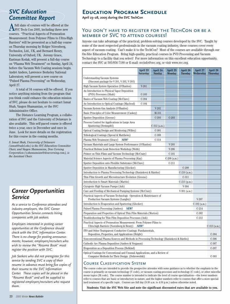
April 23 April 24 April 25 April 26 April 27 April 28Saturday Sunday Monday Tuesday Wednesday Thursday
Understanding Vacuum Systems(Discount package for V-201, V-202, V-203)
High Vacuum System Operation (O’Hanlon) V-201
An Introduction to Physical Vapor Deposition(PVD) Processes (Shah) C-103
Basics of Vacuum Web Coating (McClure) C-204
An Introduction to Optical Coatings (Macleod) C-104
Vacuum System Gas Analysis (O’Hanlon) V-202
Basic Principles of Color Measurement (Caskey) M-101
Sputter Deposition (Greene) C-203 C-203
Process Control for Applications in Large AreaSputtering (Strümpfel) C-312 (a.m.)
Optical Coating Design and Monitoring (Willey) C-301
Tribological Coatings (Sproul & Matthews) C-308
Plasma Web Treatment (Grace) NEW! C-314
Vacuum Materials and Large System Performance (O’Hanlon) V-203
Practical Helium Leak Detection Workshop (Webb) V-206
Primer on Thin Films and Vacuum Technology (McCrary) C-101
Material Science Aspects of Plasma Processing (Kay) C-209 (a.m.)
Sputter Deposition onto Flexible Substrates (McClure) C-211
Sputter Deposition in Manufacturing (Glocker) C-208
Introduction to Plasma Processing Technology (Baránková & Bárdos) C-210 (a.m.)
Thin Film Growth and Microstructure Evolution (Greene) C-311
Introduction to Smart Materials (Martin) C-213 (p.m.)
Cryogenic High Vacuum Pumps (Ash) V-304
Care and Feeding of Mechanical Pumping Systems (McCrary) V-301 (a.m.)
Practical Aspects of Vacuum Technology: Operation & Maintenance ofProduction Vacuum Systems (Langley) V-207
Introduction to Evaporation and Sputtering (Glocker) C-102 (a.m.)
Pulsed Plasma Processing (Anders) NEW! C-214
Preparation and Properties of Optical Thin Film Materials (Morton) C-302
Troubleshooting for Thin Film Deposition Processes (Ash) C-212
Practical Aspects of Permeation Measurement: From Polymer Films toUltra-high Barriers (Norenberg & Henry) NEW! C-313 (a.m.)
ITO and Other Transparent Conductive Coatings: Fundamentals,Deposition, Properties, and Applications (Bright) C-304
Nonconventional Plasma Sources and Methods in Processing Technology (Baránková & Bárdos) C-306
Cathodic Arc Plasma Deposition (Anders & Vergason) C-307
Evaporation as a Deposition Process (Belkind) C-207
Optical Coatings for Conventional and Unusual Applications, and a Review ofComputer Methods for Their Design (Dobrowolski) C-303
Course Classification SystemThe course codes are intended to provide the prospective attendee with some guidance as to whether the emphasis in thecourse is primarily on vacuum technology (V code), or vacuum coating processes and technology (C code), or other miscella-neous topics (M code). The course number is intended to indicate the level of course specialization—the lower numbersrefer to courses that are basic or introductory in nature, and the higher numbers refer to courses that offer a more special-ized treatment of a specific topic. Courses are full day (8:30 a.m. to 4:30 p.m.) unless otherwise noted.
Students: Visit the SVC Web Site and note the significant discounted rates that are available to you.
Education Program ScheduleApril 23–28, 2005 during the SVC TechCon
You don’t have to register for the TechCon or be amember of SVC to attend courses!Anyone can take advantage of the practical, problem-solving courses developed by the SVC. Taught bysome of the most respected professionals in the vacuum coating industry, these courses cover everyaspect of vacuum coating. Can’t make it to the TechCon? Most of the courses are available through ourOn-Site Education Program. Bring high-quality, practical courses in PVD Processing and VacuumTechnology to a facility that you select! For more information on this excellent education opportunity,contact the SVC at 505/856-7188 or E-mail: [email protected], or visit www.svc.org.
Career OpportunitiesServiceAs a service to Conference attendees andindustry employers, the SVC CareerOpportunities Service connects hiringcompanies with job seekers.
Employers interested in posting careeropportunities at the Conference shouldcheck with the SVC Information Center.There is no charge for posting announce-ments; however, employers/recruiters whowish to review the "Resume Book" mustregister the position with SVC.
Job Seekers who did not preregister for thisservice by sending SVC a copy of theirresume in advance must bring five copies oftheir resume to the SVC InformationCenter. These copies will be placed in the“Resume Book” and will be supplied toregistered employers/recruiters who requestthem.
SVC EducationCommittee Report
Afull slate of courses will be offered at theSVC Tech Con 2005, including three new
courses. “Practical Aspects of PermeationMeasurement: from Polymer Films to Ultra-HighBarriers” will be presented as a half-day courseon Thursday morning by Holger Nörenberg,Technolox, Ltd., UK, and Bernard Henry,University of Oxford, UK. Jeremy Grace,Eastman Kodak, will present a full-day courseon “Plasma Web Treatment” on Sunday, April 24,before the Vacuum Web Coating sessions begin.André Anders, Lawrence Berkeley NationalLaboratory, will present a new course on“Pulsed Plasma Processing” on Wednesday,April 27.
A total of 34 courses will be offered. If younotice anything missing from the program thatyou think could enhance the education missionof SVC, please do not hesitate to contact IsmatShah, Vasgen Shamamian, or the SVCAdministrative Office.
The Distance Learning Program, a collabo-ration of SVC and the University of Delaware isalso available. This self-paced course is offeredtwice a year, once in December and once inJune. Look for more details on the registrationfor this course in the coming months.
S. Ismat Shah, University of Delaware([email protected]) is the SVC Education CommitteeChair, and Vasgen Shamamian, Dow CorningCorporation ([email protected]), isthe Assistant Chair.
2005 Winter News Bulletin 21
SVC TechCon MeetingScheduleThe schedule of SVC meetings held during the48th Annual SVC TechCon in Denver is listedbelow. The SVC Education Program offerscourses starting on Saturday, April 23, andending on Thursday, April 28. See page 20 forthe detailed schedule.
Sunday, April 24 7:00 a.m.–8:30 a.m. Education Committee Breakfast Meeting10:00 a.m.–3:15 p.m. Board of Directors Lunch Meeting1:00 p.m.–4:00 p.m. Vacuum Wizard Presentations (Don McClure)3:30 p.m.–4:30 p.m. TAC Chair and Moderator AV Training Session4:30 p.m.–5:30 p.m. Newcomer’s Welcome Reception7:00 p.m.–8:45 p.m. Awards Ceremony & Plenary Session (Salil Pradhan)8:45 p.m.–10:30 p.m. Welcome Reception for TechCon Registrants
Monday, April 257:00 a.m.–8:20 a.m. TAC Breakfast Meetings8:30 a.m.–9:15 a.m. Keynote Special Presentation (Zhenan Bao)9:30 a.m.–5:00 p.m. SVC Parallel Technical Sessions (3)12:00 p.m.–7:00 p.m. Exhibit Open. Dinner Buffet at 5:30 p.m.12:40 p.m.–1:20 p.m. Donald M. Mattox Tutorial Program (Ralf Fellenberg)1:30 p.m.–4:30 p.m. Innovators Showcase Session2:10 p.m.–3:10 p.m. “Meet the Experts” Corner4:30 p.m.–7:00 p.m. Poster Session – $200 award for Best Poster!7:15 p.m.–9:15 p.m. Heureka! Late-Breaking News Session
Tuesday, April 267:00 a.m.–8:20 a.m. Technology Forum Breakfast 7:30 a.m.–8:45 a.m. Exhibitor Meeting9:30 a.m.–3:30 p.m. SVC Parallel Technical Sessions (3)10:00 a.m.–5:00 p.m. Exhibit Open. Lunch at 12:00 p.m. and Beer Blast at
3:30 p.m.12:40 p.m. –1:20 p.m. Donald M. Mattox Tutorial Program (H. Angus Macleod)2:10 p.m.–3:10 p.m. “Meet the Experts” Corner5:30 p.m.–6:30 p.m. Workshop on Specialty Coatings
Wednesday, April 277:00 a.m.–8:20 a.m. Technology Forum Breakfast 8:30 a.m.–5:00 p.m. Smart Materials Symposium 8:30 a.m.–5:00 p.m. SVC Parallel Technical Sessions (2)10:30 a.m.–12:00 p.m. “Meet the Experts” Corner12:40 p.m.–1:20 p.m. Donald M. Mattox Tutorial Program (John B. Fenn, Jr.)6:30 p.m.–10:00 p.m. Program Committee Dinner Meeting
Thursday, April 287:00 a.m.–8:20 a.m. Board of Directors Breakfast Meeting8:30 a.m.–12:00 p.m. SVC Parallel Technical Sessions (3)
TechCon registrants are invited to attend committee meetings if advance noticeis given to the SVC Administrative Office at [email protected].
For SaleStokes 72” Dia. x 110” L Vacuum Metalizer w/ support equipment
Stokes 72” Dia. x 114” L Vacuum Metalizer w/ support equipment
NRC 84” Dia. x 126” L Vacuum Metalizer w/ support equipment
C&C General L.L.C.Call Brad (231) 798-7609 E-mail: [email protected]
New! Streaming Video ClipsStreaming video clips of some of the oral history interviews are now onthe SVC Web Site at http://www.svc.org/H/Videos/H_HistoricalVideo.html. You can actually hear and see the interview in progress!
Oral History InterviewsVideo tapes of oral interviews with key individuals conducted by HistoryCommittee members can be viewed at the TechCon in the PlazaBallroom Prefunction area near Registration on Sunday throughThursday, April 24–28, 2005. The Education Resources Library also hasPowerPoint Playback files and tapes of the Plenary Address, SpecialPresentations, and some Tutorials at the 2002, 2003, and 2004 TechCons.These presentations will be available for viewing in the SVC Speakers’Room/Educational Resources Library.
New! 50th Anniversary Publication to Document HistoryDon Mattox, SVC History Committee Chair, has agreed to spearheadactivities relating to the SVC 50th Anniversary in 2007. One projectplanned is creation of a publication that will tentatively be titled “50Years of the Society of Vacuum Coaters.” It is proposed that the publica-tion will be in two parts. The first part will be the organizational historyof SVC, and the second part will be vacuum coating technology as seenby SVC interests. The goal of the SVC History Committee is to have ahard copy version of the publication available at the 50th Annual SVCTechnical Conference and to have it be published as a supplement to theConference Proceedings. This would put it into archival form both as ahard copy and in an electronic, searchable form on the SVC CD-ROM andwith Knovel.com—(where our SVC Proceedings reside). The work willalso be placed on the SVC Web Site.
Don would appreciate the help of anyone who would like to be onthe editorial team for the publication. He would welcome a volunteer orgroup of volunteers from each TAC to be the Associate Editor for theirappropriate technical subject. Thank you to Ludvik Martinu of theOptical Coating TAC, to Steve Nadel, of the Large Area Coating TAC, andto John B. Fenn, Jr., of the Vacuum Web Coating TAC, for volunteering toserve as Associate Editors for their technology! A preliminary outline ofsubject matter is available from Don Mattox.
Attention Old-Timers! We need your input. The retirees of ourvacuum coating community are the individuals who can help the HistoryCommittee and 50th Anniversary Committee fill in the blanks on theearly history of SVC.
If you are willing to contribute to the publication, please send yourcomments and contributions to Don Mattox at [email protected], orcall him at 505/856-7188.
SVC History Committee News
Thank you!The SVC would like to thank the companies sponsoring the followinghospitalities at the 2005 TechCon.
Refreshment Break Sponsors• A&N Corporation• Academy Precision Materials• Duniway Stockroom Corporation• Hauzer Techno Coating bv
Internet Café Sponsor• Varian Inc.
Beer Blast Sponsors• Dexter Magnetic Technologies, Inc.• DynaVac• GENERAL Vacuum Equipment Ltd.• Huettinger Electronic, Inc.• MKS Instruments, Inc.• Rocky Brook Associates, Inc.• Rohwedder, Inc.• SHI - APD Cryogenics, Inc.• VEECO Instruments, Inc.o

24 2005 Winter News Bulletin
Safety:Safety Aspects of Vacuum Processing
The vacuum environment poses no direct safetyhazard unless you happen to be in the chamberwhen it is pumped down. The pressure differentialthat is established between the ambient and thevacuum can cause safety hazards. If a glassenclosure, such as that of a glass belljar chamberor the envelope of an ionization gauge, breaks thenthe pressure differential will cause an implosion ofthe glass shards. In the case of the belljar, theflying glass can pose a safety hazard. This is thereason that glass belljars are not commonly usednowadays. Glass belljars can easily break if heatednon-uniformly such as having an electron beamhitting one area. If they are used, they aresurrounded by a wire enclosure to prevent theglass shards from escaping. The glass envelope ofan ionization gauge should also be surrounded byan enclosure, more to prevent it from beingaccidentally broken than it being a safety hazard.When working around systems where implosioncan occur, safety glasses should be worn.
There have been several cases of deathwhere large, vertical, top-opening vacuumchambers have been backfilled with a heavier-than-air gas, such an argon, and a person hasentered the oxygen-deficient atmosphere. In onecase, several would-be rescuers died as well asthe original victim. When situations like this arepossible the worker should have a safety-line thatallows them to be pulled out of the chamber.
Vacuum chambers are not designed forpressurization, and if backfilling from a highpressure source, such as tank nitrogen, causesthe pressure in the chamber to exceed theambient atmospheric pressure, a seal may releaseviolently causing injury or damage. This hazardcan be avoided by capturing the seal with clampsor bolts and having a pressure relief valve on thechamber. Doors should have stops that preventthem from opening more than a centimeter or sowithout removing the stop, this prevents themfrom flying open unexpectedly.
The vacuum pumping system used togenerate the vacuum poses the same safetyhazards as those commonly encountered inelectrical and mechanical equipment. Movingparts, such as belts and pulleys, should beshielded so that hands and clothing will not getcaught. High voltage leads should be shielded.Interlocks should be used to prevent the highvoltage from being turned on unless there is avacuum in the chamber. If an interlock isoverridden for maintenance reasons there shouldbe a flashing red light for everyone to see.
Liquid nitrogen is often used in vacuumtechnology to cool adsorption materials, trapsand baffles. If the liquid nitrogen vaporizes in a
poorly ventilated enclosed space it can displaceenough air to form an oxygen-deficientatmosphere. This oxygen-deficient environmentcan cause workers in the area to pass out. Oneliter of liquid nitrogen will produce about 650liters (STP) of nitrogen gas. When using liquidnitrogen, care should be taken that the cold fluidor a cold surface does not contact and “burn” theskin. In particular, liquid nitrogen should not beallowed to drop in your shoes! The liquidnitrogen can splatter, so safety glasses or a faceshield should be used when transferring the fluid.
Oxygen is used for reactive plasma cleaningand the reactive deposition of oxide compounds.Compressing pure oxygen in an oil-sealed mechan-ical pump, using hydrocarbon oil, can cause adiesel-type explosion that can blow the pumpapart. This problem can be minimized by using anoxygen-nitrogen mixture, such as pure air, that isless explosive. More chemically stable fluids, suchas silicone oil or perfluorinated polyethers (PFPE)such as Fomblin™, can be used in the mechanicalpump, but generally they are not good lubricantsand maintenance can be a problem. Pumpingpure oxygen in a cryopump followed by pumpinghydrogen, such as is formed by the decompositionof a hydrocarbon vapor in the reactive depositionof a carbide film, can cause an explosion in thecryopump on regeneration.
Plasmas, along with high voltages, can posea safety problem if a metal vacuum chamber isnot adequately grounded. A plasma in contactwith a surface at a high negative voltage can floatto a high negative potential with respect toground. If an electrically floating surface, such asa metal vacuum chamber isolated from ground bya rubber sealing gasket, is in contact with theplasma it can attain a high voltage with respectto ground. This can present a shocking hazard.High voltages in contact with the plasma cancome from such diverse sources as bias voltageson substrates or ionization gauges that are lefton, particularly in the degas mode, when theplasma is established. All metal surfaces inplasma systems that are not being used aselectrodes should be well grounded to preventsuch floating potentials.
Plasmas generate ultraviolet radiation thatcan be transmitted through glass windows, partic-ularly if the window is quartz. Ultraviolet radiationcan harm eyes and skin on excessive exposure. TheUV can be adsorbed by filters on the windows or byeye glasses worn by the operator. These are thesame types of glasses used when working withlasers or with glass blowing.
In thermal evaporation the material beingevaporated is at a high temperature and thethermal radiation can harm skin and eyes, partic-ularly those wearing contact lenses. An opticallyclear “heat mirror”, which transmits the visible
Sample Guide from the Collection ofEducation Guides to Vacuum Coating Processingby Donald M. MattoxSVC Technical Director
Order YourEducation
Guides Today!Written by Donald M. Mattox, SVCTechnical Director, this indispensiblepublication contains individual, stand-alone, two-page guides on differentaspects of the equipment and technologyassociated with vacuum coatingprocessing by physical vapor deposition.Titles of some of the sections include:
• Introduction to the Basics ofPVD Processing
• Materials Science
• Vacuum Technology
• Plasma Technology
• Surface Preparation
• Vacuum Evaporation
• Sputter Deposition
• Arc Vapor Deposition
• Ion Plating
• Low-Pressure CVD and PECVD
• Atomistic Film Growth andResulting Film Properties
• Surface and FilmCharacterization
• Applications
• Safety
More than 90 Guides inOne Set With Updates
Added Every Year!
Each set is only $50(includes shipping/handling in USA)
$35 each for 10 or more sets
For a complete list of titles and orderinginformation, visit the SVC Web Site at:http://www.svc.org/EP/EP_Educational
Guides.html.
You can also send us anE-mail at [email protected] or call
505/856-7188 to request an order form.
Society of Vacuum Coaters71 Pinon Hill Place NEAlbuquerque, NM 87122-1914Telephone 505/856-7188Fax 505/856-6716E-mail [email protected] Site www.svc.org
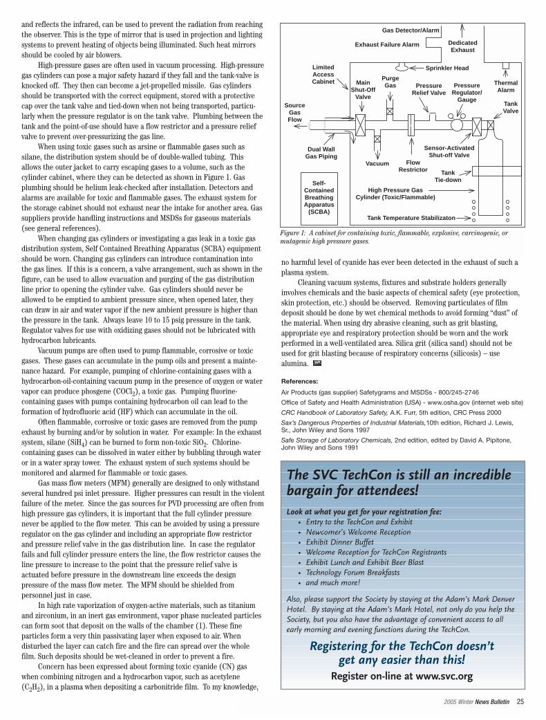
2005 Winter News Bulletin 25
and reflects the infrared, can be used to prevent the radiation from reachingthe observer. This is the type of mirror that is used in projection and lightingsystems to prevent heating of objects being illuminated. Such heat mirrorsshould be cooled by air blowers.
High-pressure gases are often used in vacuum processing. High-pressuregas cylinders can pose a major safety hazard if they fall and the tank-valve isknocked off. They then can become a jet-propelled missile. Gas cylindersshould be transported with the correct equipment, stored with a protectivecap over the tank valve and tied-down when not being transported, particu-larly when the pressure regulator is on the tank valve. Plumbing between thetank and the point-of-use should have a flow restrictor and a pressure reliefvalve to prevent over-pressurizing the gas line.
When using toxic gases such as arsine or flammable gases such assilane, the distribution system should be of double-walled tubing. Thisallows the outer jacket to carry escaping gases to a volume, such as thecylinder cabinet, where they can be detected as shown in Figure 1. Gasplumbing should be helium leak-checked after installation. Detectors andalarms are available for toxic and flammable gases. The exhaust system forthe storage cabinet should not exhaust near the intake for another area. Gassuppliers provide handling instructions and MSDSs for gaseous materials(see general references).
When changing gas cylinders or investigating a gas leak in a toxic gasdistribution system, Self Contained Breathing Apparatus (SCBA) equipmentshould be worn. Changing gas cylinders can introduce contamination intothe gas lines. If this is a concern, a valve arrangement, such as shown in thefigure, can be used to allow evacuation and purging of the gas distributionline prior to opening the cylinder valve. Gas cylinders should never beallowed to be emptied to ambient pressure since, when opened later, theycan draw in air and water vapor if the new ambient pressure is higher thanthe pressure in the tank. Always leave 10 to 15 psig pressure in the tank.Regulator valves for use with oxidizing gases should not be lubricated withhydrocarbon lubricants.
Vacuum pumps are often used to pump flammable, corrosive or toxicgases. These gases can accumulate in the pump oils and present a mainte-nance hazard. For example, pumping of chlorine-containing gases with ahydrocarbon-oil-containing vacuum pump in the presence of oxygen or watervapor can produce phosgene (COCl2), a toxic gas. Pumping fluorine-containing gases with pumps containing hydrocarbon oil can lead to theformation of hydrofluoric acid (HF) which can accumulate in the oil.
Often flammable, corrosive or toxic gases are removed from the pumpexhaust by burning and/or by solution in water. For example: In the exhaustsystem, silane (SiH4) can be burned to form non-toxic SiO2. Chlorine-containing gases can be dissolved in water either by bubbling through wateror in a water spray tower. The exhaust system of such systems should bemonitored and alarmed for flammable or toxic gases.
Gas mass flow meters (MFM) generally are designed to only withstandseveral hundred psi inlet pressure. Higher pressures can result in the violentfailure of the meter. Since the gas sources for PVD processing are often fromhigh pressure gas cylinders, it is important that the full cylinder pressurenever be applied to the flow meter. This can be avoided by using a pressureregulator on the gas cylinder and including an appropriate flow restrictorand pressure relief valve in the gas distribution line. In case the regulatorfails and full cylinder pressure enters the line, the flow restrictor causes theline pressure to increase to the point that the pressure relief valve isactuated before pressure in the downstream line exceeds the designpressure of the mass flow meter. The MFM should be shielded frompersonnel just in case.
In high rate vaporization of oxygen-active materials, such as titaniumand zirconium, in an inert gas environment, vapor phase nucleated particlescan form soot that deposit on the walls of the chamber (1). These fineparticles form a very thin passivating layer when exposed to air. Whendisturbed the layer can catch fire and the fire can spread over the wholefilm. Such deposits should be wet-cleaned in order to prevent a fire.
Concern has been expressed about forming toxic cyanide (CN) gaswhen combining nitrogen and a hydrocarbon vapor, such as acetylene(C2H2), in a plasma when depositing a carbonitride film. To my knowledge,
no harmful level of cyanide has ever been detected in the exhaust of such aplasma system.
Cleaning vacuum systems, fixtures and substrate holders generallyinvolves chemicals and the basic aspects of chemical safety (eye protection,skin protection, etc.) should be observed. Removing particulates of filmdeposit should be done by wet chemical methods to avoid forming “dust” ofthe material. When using dry abrasive cleaning, such as grit blasting,appropriate eye and respiratory protection should be worn and the workperformed in a well-ventilated area. Silica grit (silica sand) should not beused for grit blasting because of respiratory concerns (silicosis) – usealumina.
References:
Air Products (gas supplier) Safetygrams and MSDSs - 800/245-2746
Office of Safety and Health Administration (USA) - www.osha.gov (internet web site)
CRC Handbook of Laboratory Safety, A.K. Furr, 5th edition, CRC Press 2000
Sax’s Dangerous Properties of Industrial Materials,10th edition, Richard J. Lewis,Sr., John Wiley and Sons 1997
Safe Storage of Laboratory Chemicals, 2nd edition, edited by David A. Pipitone,John Wiley and Sons 1991
Self-ContainedBreathingApparatus
(SCBA)
Dual WallGas Piping
SourceGasFlow
LimitedAccessCabinet
Gas Detector/Alarm
Exhaust Failure Alarm DedicatedExhaust
MainShut-Off
Valve
PurgeGas
Sprinkler Head
PressureRelief Valve
PressureRegulator/
Gauge
Thermal Alarm
TankValve
Vacuum FlowRestrictor
Sensor-ActivatedShut-off Valve
TankTie-down
High Pressure GasCylinder (Toxic/Flammable)
Tank Temperature Stabilizaton
Figure 1: A cabinet for containing toxic, flammable, explosive, carcinogenic, ormutagenic high pressure gases.
Registering for the TechCon doesn’tget any easier than this!
Register on-line at www.svc.org
The SVC TechCon is still an incrediblebargain for attendees!Look at what you get for your registration fee:
• Entry to the TechCon and Exhibit• Newcomer’s Welcome Reception• Exhibit Dinner Buffet• Welcome Reception for TechCon Registrants• Exhibit Lunch and Exhibit Beer Blast• Technology Forum Breakfasts• and much more!
Also, please support the Society by staying at the Adam’s Mark DenverHotel. By staying at the Adam’s Mark Hotel, not only do you help theSociety, but you also have the advantage of convenient access to allearly morning and evening functions during the TechCon.
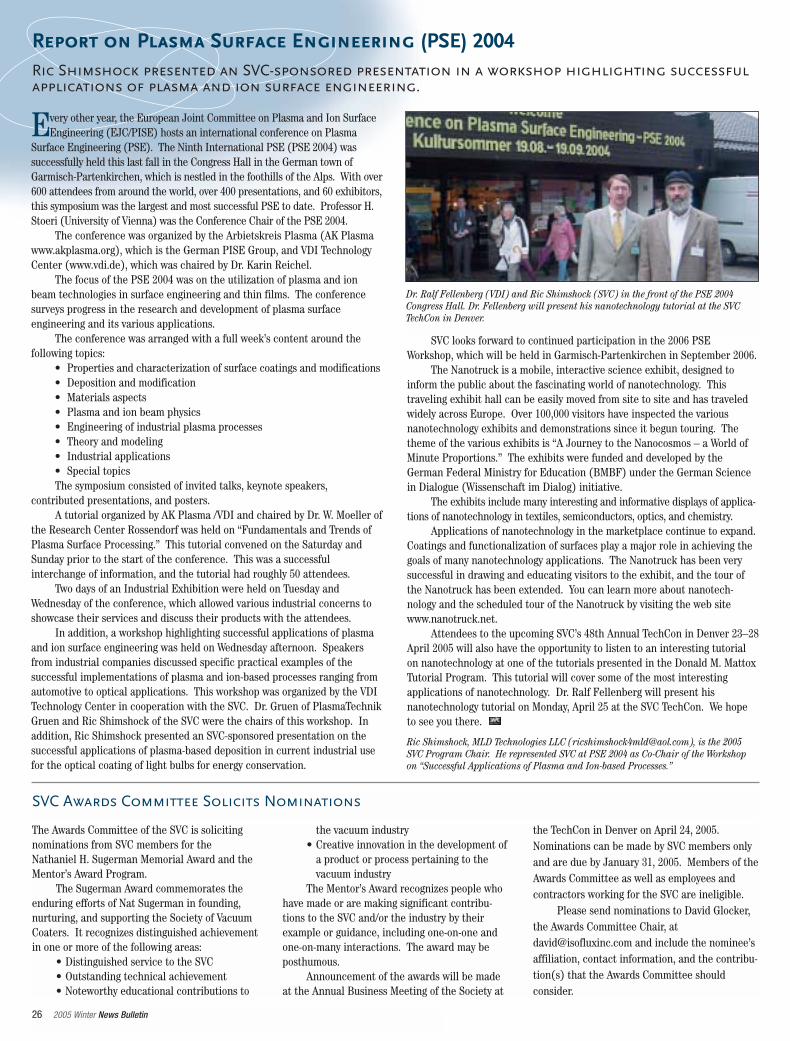
26 2005 Winter News Bulletin
Every other year, the European Joint Committee on Plasma and Ion SurfaceEngineering (EJC/PISE) hosts an international conference on Plasma
Surface Engineering (PSE). The Ninth International PSE (PSE 2004) wassuccessfully held this last fall in the Congress Hall in the German town ofGarmisch-Partenkirchen, which is nestled in the foothills of the Alps. With over600 attendees from around the world, over 400 presentations, and 60 exhibitors,this symposium was the largest and most successful PSE to date. Professor H.Stoeri (University of Vienna) was the Conference Chair of the PSE 2004.
The conference was organized by the Arbietskreis Plasma (AK Plasmawww.akplasma.org), which is the German PISE Group, and VDI TechnologyCenter (www.vdi.de), which was chaired by Dr. Karin Reichel.
The focus of the PSE 2004 was on the utilization of plasma and ionbeam technologies in surface engineering and thin films. The conferencesurveys progress in the research and development of plasma surfaceengineering and its various applications.
The conference was arranged with a full week’s content around thefollowing topics:
• Properties and characterization of surface coatings and modifications• Deposition and modification• Materials aspects• Plasma and ion beam physics• Engineering of industrial plasma processes• Theory and modeling• Industrial applications• Special topicsThe symposium consisted of invited talks, keynote speakers,
contributed presentations, and posters.A tutorial organized by AK Plasma /VDI and chaired by Dr. W. Moeller of
the Research Center Rossendorf was held on “Fundamentals and Trends ofPlasma Surface Processing.” This tutorial convened on the Saturday andSunday prior to the start of the conference. This was a successfulinterchange of information, and the tutorial had roughly 50 attendees.
Two days of an Industrial Exhibition were held on Tuesday andWednesday of the conference, which allowed various industrial concerns toshowcase their services and discuss their products with the attendees.
In addition, a workshop highlighting successful applications of plasmaand ion surface engineering was held on Wednesday afternoon. Speakersfrom industrial companies discussed specific practical examples of thesuccessful implementations of plasma and ion-based processes ranging fromautomotive to optical applications. This workshop was organized by the VDITechnology Center in cooperation with the SVC. Dr. Gruen of PlasmaTechnikGruen and Ric Shimshock of the SVC were the chairs of this workshop. Inaddition, Ric Shimshock presented an SVC-sponsored presentation on thesuccessful applications of plasma-based deposition in current industrial usefor the optical coating of light bulbs for energy conservation.
SVC looks forward to continued participation in the 2006 PSEWorkshop, which will be held in Garmisch-Partenkirchen in September 2006.
The Nanotruck is a mobile, interactive science exhibit, designed toinform the public about the fascinating world of nanotechnology. Thistraveling exhibit hall can be easily moved from site to site and has traveledwidely across Europe. Over 100,000 visitors have inspected the variousnanotechnology exhibits and demonstrations since it begun touring. Thetheme of the various exhibits is “A Journey to the Nanocosmos – a World ofMinute Proportions.” The exhibits were funded and developed by theGerman Federal Ministry for Education (BMBF) under the German Sciencein Dialogue (Wissenschaft im Dialog) initiative.
The exhibits include many interesting and informative displays of applica-tions of nanotechnology in textiles, semiconductors, optics, and chemistry.
Applications of nanotechnology in the marketplace continue to expand.Coatings and functionalization of surfaces play a major role in achieving thegoals of many nanotechnology applications. The Nanotruck has been verysuccessful in drawing and educating visitors to the exhibit, and the tour ofthe Nanotruck has been extended. You can learn more about nanotech-nology and the scheduled tour of the Nanotruck by visiting the web sitewww.nanotruck.net.
Attendees to the upcoming SVC’s 48th Annual TechCon in Denver 23–28April 2005 will also have the opportunity to listen to an interesting tutorialon nanotechnology at one of the tutorials presented in the Donald M. MattoxTutorial Program. This tutorial will cover some of the most interestingapplications of nanotechnology. Dr. Ralf Fellenberg will present hisnanotechnology tutorial on Monday, April 25 at the SVC TechCon. We hopeto see you there.
Ric Shimshock, MLD Technologies LLC ([email protected]), is the 2005SVC Program Chair. He represented SVC at PSE 2004 as Co-Chair of the Workshopon “Successful Applications of Plasma and Ion-based Processes.”
Report on Plasma Surface Engineering (PSE) 2004Ric Shimshock presented an SVC-sponsored presentation in a workshop highlighting successfulapplications of plasma and ion surface engineering.
Dr. Ralf Fellenberg (VDI) and Ric Shimshock (SVC) in the front of the PSE 2004Congress Hall. Dr. Fellenberg will present his nanotechnology tutorial at the SVCTechCon in Denver.
The Awards Committee of the SVC is solicitingnominations from SVC members for theNathaniel H. Sugerman Memorial Award and theMentor’s Award Program.
The Sugerman Award commemorates theenduring efforts of Nat Sugerman in founding,nurturing, and supporting the Society of VacuumCoaters. It recognizes distinguished achievementin one or more of the following areas:
• Distinguished service to the SVC• Outstanding technical achievement• Noteworthy educational contributions to
the vacuum industry• Creative innovation in the development of
a product or process pertaining to thevacuum industry
The Mentor’s Award recognizes people whohave made or are making significant contribu-tions to the SVC and/or the industry by theirexample or guidance, including one-on-one andone-on-many interactions. The award may beposthumous.
Announcement of the awards will be madeat the Annual Business Meeting of the Society at
the TechCon in Denver on April 24, 2005.Nominations can be made by SVC members onlyand are due by January 31, 2005. Members of theAwards Committee as well as employees andcontractors working for the SVC are ineligible.
Please send nominations to David Glocker,the Awards Committee Chair, [email protected] and include the nominee’saffiliation, contact information, and the contribu-tion(s) that the Awards Committee shouldconsider.
SVC Awards Committee Solicits Nominations
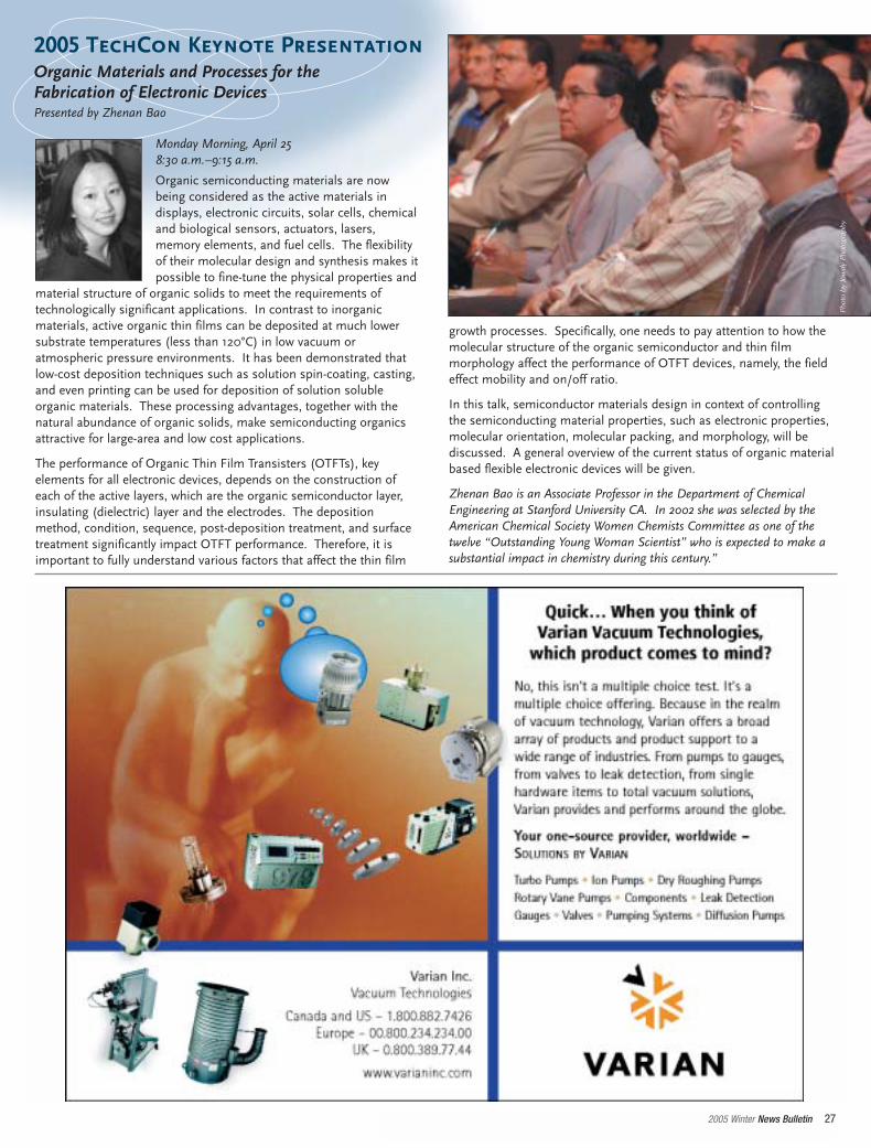
2005 Winter News Bulletin 27
Monday Morning, April 258:30 a.m.–9:15 a.m.
Organic semiconducting materials are nowbeing considered as the active materials indisplays, electronic circuits, solar cells, chemicaland biological sensors, actuators, lasers,memory elements, and fuel cells. The flexibilityof their molecular design and synthesis makes itpossible to fine-tune the physical properties and
material structure of organic solids to meet the requirements oftechnologically significant applications. In contrast to inorganicmaterials, active organic thin films can be deposited at much lowersubstrate temperatures (less than 120°C) in low vacuum oratmospheric pressure environments. It has been demonstrated thatlow-cost deposition techniques such as solution spin-coating, casting,and even printing can be used for deposition of solution solubleorganic materials. These processing advantages, together with thenatural abundance of organic solids, make semiconducting organicsattractive for large-area and low cost applications.
The performance of Organic Thin Film Transisters (OTFTs), keyelements for all electronic devices, depends on the construction ofeach of the active layers, which are the organic semiconductor layer,insulating (dielectric) layer and the electrodes. The depositionmethod, condition, sequence, post-deposition treatment, and surfacetreatment significantly impact OTFT performance. Therefore, it isimportant to fully understand various factors that affect the thin film
growth processes. Specifically, one needs to pay attention to how themolecular structure of the organic semiconductor and thin filmmorphology affect the performance of OTFT devices, namely, the fieldeffect mobility and on/off ratio.
In this talk, semiconductor materials design in context of controllingthe semiconducting material properties, such as electronic properties,molecular orientation, molecular packing, and morphology, will bediscussed. A general overview of the current status of organic materialbased flexible electronic devices will be given.
Zhenan Bao is an Associate Professor in the Department of ChemicalEngineering at Stanford University CA. In 2002 she was selected by theAmerican Chemical Society Women Chemists Committee as one of thetwelve “Outstanding Young Woman Scientist” who is expected to make asubstantial impact in chemistry during this century.”
2005 TechCon Keynote PresentationOrganic Materials and Processes for theFabrication of Electronic DevicesPresented by Zhenan Bao
Phot
o by
Jow
dy P
hoto
grap
hy
28 2005 Winter News Bulletin
Introduction
During the 16th Century, a secret process to produce mirrors of a qualitynever before seen was devised in Venice. The mirrors consisted of a glasssubstrate carrying on their rear surface a layer of mercury-tin amalgam. Inspite of vigorous attempts it proved impossible to retain the secret and thetechnique spread. Mirrors became an important feature of interior design.This was the beginning of the modern optical coating industry. Nowadays,optical coatings have penetrated every corner of our modern lives. From the$20 bill in our pocket to the DVD player in our home, optical coatings play acritical role.
Optical coatings modify the optical properties of surfaces. Most oftenthese are the carefully worked surfaces that shape and direct the light raysin an optical system but they can also be applied to other surfaces, often in adecorative mode. Their operation relies on interference effects combinedwith the optical properties of their materials. This account is necessarilylimited to some of the more common coating types.
Fundamental parameters
In free space, the propagation of an electromagnetic wave is independent ofwavelength or frequency. There are two principal parameters that charac-terize this propagation. Both are exact and are fundamental physicalconstants. The first is the velocity of light in vacuum, c, of value 299,792,458 msec-1, and the second, the permeability of vacuum, µ0, of value 4π×10-7 N/A2.
Propagation of an electromagnetic wave in an optical material is a littlemore complicated. The shape of any arbitrary wave changes as it propagatesmaking it difficult to assign a velocity to it. Fortunately at normal powerlevels the phenomena are purely linear. That means that we can representthe light as a spectrum of harmonic components that can be treatedseparately and do not change shape as they propagate. We are so used to thisprocess that we scarcely think about it. The spectral components that we usein the thin-film field are infinite, plane, harmonic waves, that is they are aharmonic function of time and distance along the direction of propagationonly. The electric field, magnetic field and direction of propagation in thesewaves are mutually perpendicular and form what is called a right-handed set.The orientation of the electric vector is described by the term polarization.We will use the simplest form, called linear, or sometimes plane, polarization,where the electric vector is constant in direction.
In an optical material the light interacts with the electrons so that itspropagation characteristics are altered. We could build our theories of opticalbehavior using the velocity of light, v, and the permeability, µ, associated witha harmonic wave, to characterize our materials, but the results are a great dealless clumsy if we introduce two related parameters. The first is the refractiveindex, the ratio of the velocity of light in free space to the velocity in thematerial, c/v, written as n. The other is the characteristic admittance of thematerial, written as y and of value 1/(vµ). The characteristic admittancerepresents the ratio of the magnetic to the electric field amplitudes of apropagating harmonic wave. In free space, n is unity and y is 0.002654419 S(siemens). The electrical engineer usually prefers to use the characteristicimpedance, z, of value 376.73031 Ω (ohm) in free space.
There is an enormous simplification in optics because the frequenciesare so high that there is no direct magnetic interaction with the electronsthat are responsible for the optical properties of materials. This means thatthe permeability, µ, of the material remains at the value of µ0. This impliesthat y is simply n times the admittance of free space, or n free space units,and allows us to use the same number for both quantities. Note that y and nare only numerically equal and not physically equal.
The effects we are dealing with are linear and so the frequency of thewave is constant. This means if it slows down then the wavelength is reducedin proportion. We avoid problems by using the wavelength in free space to
characterize the wave. This wavelength is n times the actual wavelength andimplies that we have to make the same adjustments to the distance, d, andso we introduce the quantity nd known as the optical thickness. When wetalk of the thickness of a film in an optical coating, generally we imply theoptical rather than the physical thickness.
n governs refraction at a boundary between two materials throughSnell’s Law:
where ϑ is the angle between the ray and the surface normal. n is alsoinvolved, through the optical thickness, in the change of phase due topropagation through a material. If the physical thickness is d, then δ, knownas the phase thickness, is given by
where λ is the wavelength measured in free space. y characterizes theamount of light reflected at a boundary between two media. The ratio of thereflected amplitude to the incident amplitude is given by:
In dielectric materials the electrons are bound. They accept energyfrom the electric field but then radiate it back and the principal effect is aslowing down of the light so that the refractive index, n, is greater thanunity. In metals the free electrons extract energy from the electric field butdo not return the energy to the wave. The amplitude of the propagating wavedecays exponentially. The decay is usually expressed as exp(-2πkd/λ) wherek is dimensionless and known as the extinction coefficient. An extinctioncoefficient can also be used to characterize the small residual losses in adielectric material. In an ideal metal the light wave suffers no change inphase as it propagates. In a real metal there is a phase change, often quitesmall, and this can be associated with a refractive index through equation(2). A quite small refractive index can be mistakenly taken as an indicationthat the light is traveling faster than its speed in free space. We must notforget that we are dealing with an infinite harmonic wave in a steady-statecondition and that the refractive index is derived from a steady-state phasedifference. A pulse of light is a transient effect with quite different behavior.
Provided that the effects are linear, we can conveniently combine thecosine and sine representation of a harmonic wave into a complex form,known as a complex wave.
The quantity (n-ik) appearing in the right-hand side of equation (4) isknown as the complex refractive index. As long as we stick to linearoperations, like addition or subtraction or multiplication by a real constant,there is never any mixing of the real and imaginary parts of expression (4)and it is much simpler to use the right-hand side of (4) than either of theterms on the left-hand side. y, the characteristic admittance is then equal to(n-ik) free space units. All the previous relationships work equally well withcomplex arguments.
Fundamentals of Optical Coatingsby Angus MacleodThin Film Center Inc.
n n0 0 1 1sin sinϑ ϑ= (1)
δ πλ
= 2 nd (2)
ρ = −+
y y
y y0 1
0 1
(3)
E Eexp cos exp sin−
−
+ −
−2 2 2 2πλ
ω πλ
πλ
ωkzt
nzi
kzt
πλ
ωπ
λ
nz
i tn ik z
= −−( )
Eexp2
(4)
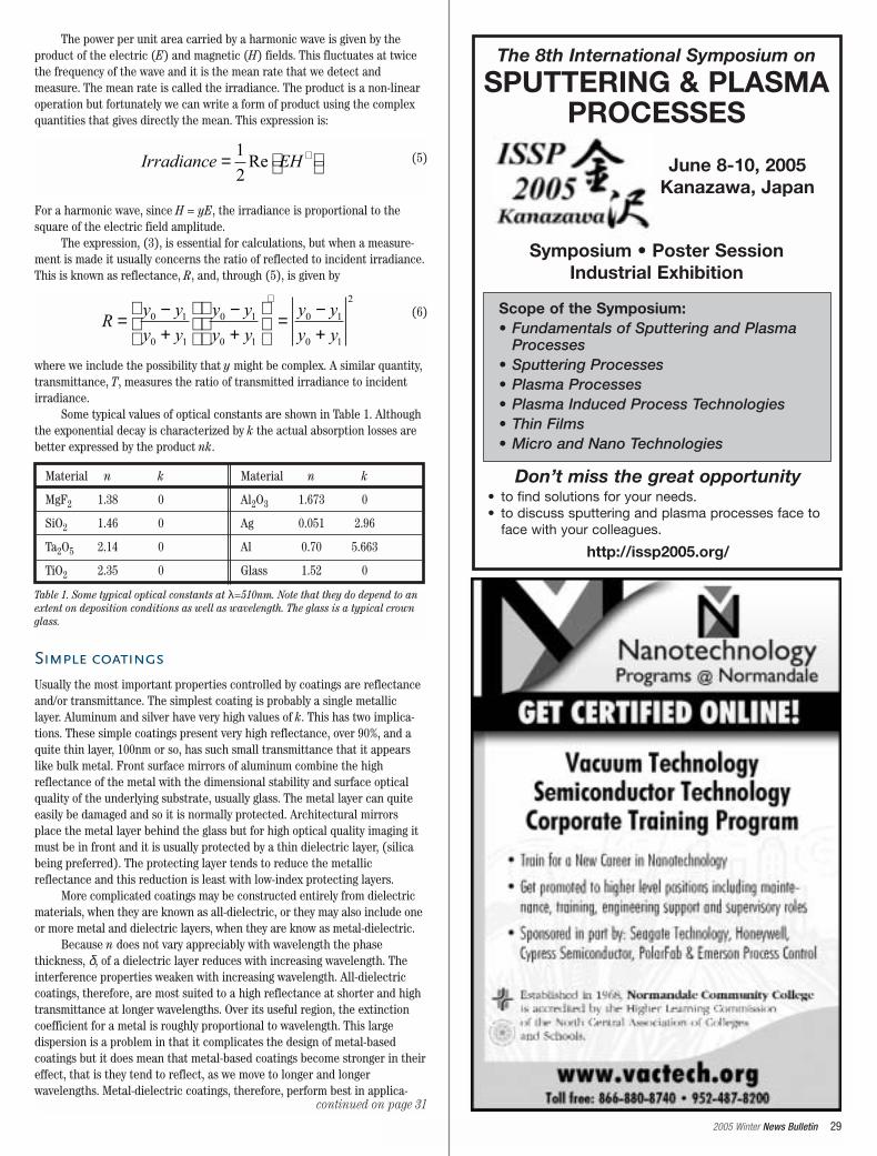
2005 Winter News Bulletin 29
The power per unit area carried by a harmonic wave is given by theproduct of the electric (E) and magnetic (H) fields. This fluctuates at twicethe frequency of the wave and it is the mean rate that we detect andmeasure. The mean rate is called the irradiance. The product is a non-linearoperation but fortunately we can write a form of product using the complexquantities that gives directly the mean. This expression is:
For a harmonic wave, since H = yE, the irradiance is proportional to thesquare of the electric field amplitude.
The expression, (3), is essential for calculations, but when a measure-ment is made it usually concerns the ratio of reflected to incident irradiance.This is known as reflectance, R, and, through (5), is given by
where we include the possibility that y might be complex. A similar quantity,transmittance, T, measures the ratio of transmitted irradiance to incidentirradiance.
Some typical values of optical constants are shown in Table 1. Althoughthe exponential decay is characterized by k the actual absorption losses arebetter expressed by the product nk.
Simple coatings
Usually the most important properties controlled by coatings are reflectanceand/or transmittance. The simplest coating is probably a single metalliclayer. Aluminum and silver have very high values of k. This has two implica-tions. These simple coatings present very high reflectance, over 90%, and aquite thin layer, 100nm or so, has such small transmittance that it appearslike bulk metal. Front surface mirrors of aluminum combine the highreflectance of the metal with the dimensional stability and surface opticalquality of the underlying substrate, usually glass. The metal layer can quiteeasily be damaged and so it is normally protected. Architectural mirrorsplace the metal layer behind the glass but for high optical quality imaging itmust be in front and it is usually protected by a thin dielectric layer, (silicabeing preferred). The protecting layer tends to reduce the metallicreflectance and this reduction is least with low-index protecting layers.
More complicated coatings may be constructed entirely from dielectricmaterials, when they are known as all-dielectric, or they may also include oneor more metal and dielectric layers, when they are know as metal-dielectric.
Because n does not vary appreciably with wavelength the phasethickness, δ, of a dielectric layer reduces with increasing wavelength. Theinterference properties weaken with increasing wavelength. All-dielectriccoatings, therefore, are most suited to a high reflectance at shorter and hightransmittance at longer wavelengths. Over its useful region, the extinctioncoefficient for a metal is roughly proportional to wavelength. This largedispersion is a problem in that it complicates the design of metal-basedcoatings but it does mean that metal-based coatings become stronger in theireffect, that is they tend to reflect, as we move to longer and longerwavelengths. Metal-dielectric coatings, therefore, perform best in applica-
continued on page 31
Irradiance EH= ∗1
2Re (5)
Ry y
y y
y y
y y
y y
y y= −
+
−+
= −
+
∗
0 1
0 1
0 1
0 1
0 1
0 1
2(6)
Material n k Material n k
MgF2 1.38 0 Al2O3 1.673 0
SiO2 1.46 0 Ag 0.051 2.96
Ta2O5 2.14 0 Al 0.70 5.663
TiO2 2.35 0 Glass 1.52 0
Table 1. Some typical optical constants at λ=510nm. Note that they do depend to anextent on deposition conditions as well as wavelength. The glass is a typical crownglass.
The 8th International Symposium on
SPUTTERING & PLASMAPROCESSES
June 8-10, 2005Kanazawa, Japan
Symposium • Poster SessionIndustrial Exhibition
Don’t miss the great opportunity• to find solutions for your needs.• to discuss sputtering and plasma processes face to
face with your colleagues.
http://issp2005.org/
Scope of the Symposium:• Fundamentals of Sputtering and Plasma
Processes• Sputtering Processes• Plasma Processes• Plasma Induced Process Technologies• Thin Films• Micro and Nano Technologies
What’s Aheadfor the Vacuum
Coating Industry?
What’s Aheadfor the Vacuum
Coating Industry?
Stay Updated
Pho
tos
of
Den
ver
cour
tesy
of
the
Den
ver
Met
ro C
onv
entio
n &
Vis
itors
Bur
eau
48th Annual SVC Technical Conferenceand Smart Materials Symposium
48th Annual SVC Technical Conferenceand Smart Materials Symposium
Society of Vacuum Coaters 505/856-7188 Fax 505/856-6716 E-mail [email protected]
Join us in the “Mile High City” for six days ofeducation, innovation, and information onvacuum coating!Exciting developments and innovative ideas will be presented in the Technical Sessions
(April 25–28), including the second annual Smart Materials Symposium, co-sponsored byElsevier, as well as two Hot Topic Joint Sessions, a special HIPIMS Session, Heuréka! Post-
Deadline Recent Development Session, and much more. Other highlights include the Donald M. MattoxTutorial Program, “Meet the Experts” Corner, Technology Forum Breakfasts, the Internet Cafe and Beer Blast
in the Exhibit Hall, and various other hospitality events – all included in the registration fee.
The two-day Exhibit & Innovators Showcase (April 25–26) is a one-of-a-kind forumdedicated to showcasing technological advances in the vacuum coating industry.
Take advantage of the SVC Short Course Education Program (April 23–28) during the TechCon. Youdon’t need to register for the TechCon or be an SVC member to choose from more than 30 high-quality,
practical courses taught by industry experts.
www.svc.org
SV
C P
hoto
s b
y Jo
wd
y P
hoto
gra
phy
April 23–28, 2005Adam’s Mark Denver Hotel
Denver, Colorado
April 23–28, 2005Adam’s Mark Denver Hotel
Denver, Colorado
For more information, go to
to find out more about this one-of-a-kind event.
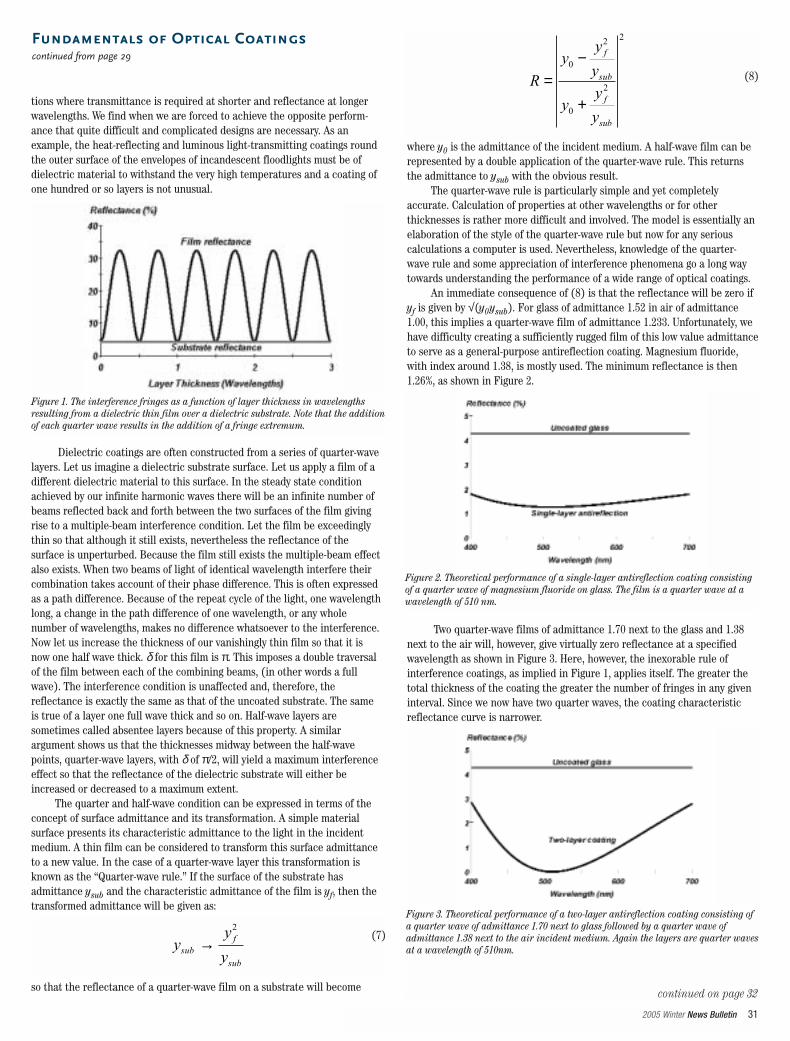
2005 Winter News Bulletin 31
tions where transmittance is required at shorter and reflectance at longerwavelengths. We find when we are forced to achieve the opposite perform-ance that quite difficult and complicated designs are necessary. As anexample, the heat-reflecting and luminous light-transmitting coatings roundthe outer surface of the envelopes of incandescent floodlights must be ofdielectric material to withstand the very high temperatures and a coating ofone hundred or so layers is not unusual.
Dielectric coatings are often constructed from a series of quarter-wavelayers. Let us imagine a dielectric substrate surface. Let us apply a film of adifferent dielectric material to this surface. In the steady state conditionachieved by our infinite harmonic waves there will be an infinite number ofbeams reflected back and forth between the two surfaces of the film givingrise to a multiple-beam interference condition. Let the film be exceedinglythin so that although it still exists, nevertheless the reflectance of thesurface is unperturbed. Because the film still exists the multiple-beam effectalso exists. When two beams of light of identical wavelength interfere theircombination takes account of their phase difference. This is often expressedas a path difference. Because of the repeat cycle of the light, one wavelengthlong, a change in the path difference of one wavelength, or any wholenumber of wavelengths, makes no difference whatsoever to the interference.Now let us increase the thickness of our vanishingly thin film so that it isnow one half wave thick. δ for this film is π. This imposes a double traversalof the film between each of the combining beams, (in other words a fullwave). The interference condition is unaffected and, therefore, thereflectance is exactly the same as that of the uncoated substrate. The sameis true of a layer one full wave thick and so on. Half-wave layers aresometimes called absentee layers because of this property. A similarargument shows us that the thicknesses midway between the half-wavepoints, quarter-wave layers, with δ of π/2, will yield a maximum interferenceeffect so that the reflectance of the dielectric substrate will either beincreased or decreased to a maximum extent.
The quarter and half-wave condition can be expressed in terms of theconcept of surface admittance and its transformation. A simple materialsurface presents its characteristic admittance to the light in the incidentmedium. A thin film can be considered to transform this surface admittanceto a new value. In the case of a quarter-wave layer this transformation isknown as the “Quarter-wave rule.” If the surface of the substrate hasadmittance ysub and the characteristic admittance of the film is yf, then thetransformed admittance will be given as:
so that the reflectance of a quarter-wave film on a substrate will become
where y0 is the admittance of the incident medium. A half-wave film can berepresented by a double application of the quarter-wave rule. This returnsthe admittance to ysub with the obvious result.
The quarter-wave rule is particularly simple and yet completelyaccurate. Calculation of properties at other wavelengths or for otherthicknesses is rather more difficult and involved. The model is essentially anelaboration of the style of the quarter-wave rule but now for any seriouscalculations a computer is used. Nevertheless, knowledge of the quarter-wave rule and some appreciation of interference phenomena go a long waytowards understanding the performance of a wide range of optical coatings.
An immediate consequence of (8) is that the reflectance will be zero ifyf is given by √(y0ysub). For glass of admittance 1.52 in air of admittance1.00, this implies a quarter-wave film of admittance 1.233. Unfortunately, wehave difficulty creating a sufficiently rugged film of this low value admittanceto serve as a general-purpose antireflection coating. Magnesium fluoride,with index around 1.38, is mostly used. The minimum reflectance is then1.26%, as shown in Figure 2.
Two quarter-wave films of admittance 1.70 next to the glass and 1.38next to the air will, however, give virtually zero reflectance at a specifiedwavelength as shown in Figure 3. Here, however, the inexorable rule ofinterference coatings, as implied in Figure 1, applies itself. The greater thetotal thickness of the coating the greater the number of fringes in any giveninterval. Since we now have two quarter waves, the coating characteristicreflectance curve is narrower.
continued on page 32
Fundamentals of Optical Coatingscontinued from page 29
Figure 2. Theoretical performance of a single-layer antireflection coating consistingof a quarter wave of magnesium fluoride on glass. The film is a quarter wave at awavelength of 510 nm.
Figure 3. Theoretical performance of a two-layer antireflection coating consisting ofa quarter wave of admittance 1.70 next to glass followed by a quarter wave ofadmittance 1.38 next to the air incident medium. Again the layers are quarter wavesat a wavelength of 510nm.
Figure 1. The interference fringes as a function of layer thickness in wavelengthsresulting from a dielectric thin film over a dielectric substrate. Note that the additionof each quarter wave results in the addition of a fringe extremum.
yy
ysubf
sub
→2
(7)
R
yy
y
yy
y
f
sub
f
sub
=−
+
0
2
0
2
2
(8)
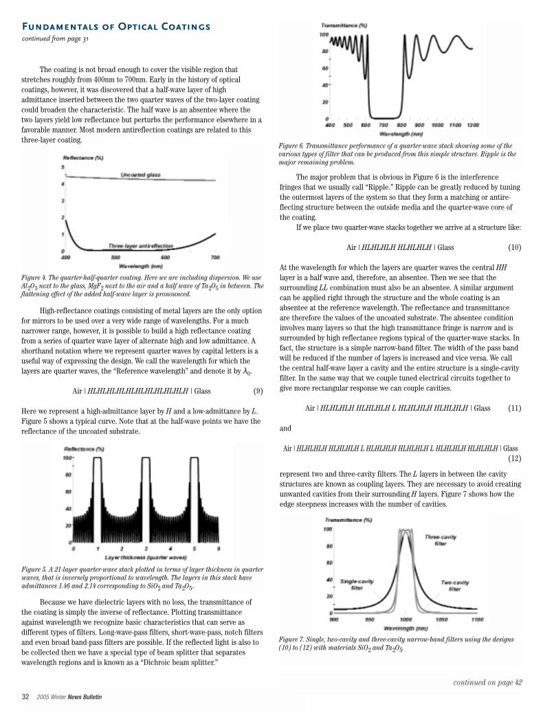
32 2005 Winter News Bulletin
The coating is not broad enough to cover the visible region thatstretches roughly from 400nm to 700nm. Early in the history of opticalcoatings, however, it was discovered that a half-wave layer of highadmittance inserted between the two quarter waves of the two-layer coatingcould broaden the characteristic. The half wave is an absentee where thetwo layers yield low reflectance but perturbs the performance elsewhere in afavorable manner. Most modern antireflection coatings are related to thisthree-layer coating.
High-reflectance coatings consisting of metal layers are the only optionfor mirrors to be used over a very wide range of wavelengths. For a muchnarrower range, however, it is possible to build a high reflectance coatingfrom a series of quarter wave layer of alternate high and low admittance. Ashorthand notation where we represent quarter waves by capital letters is auseful way of expressing the design. We call the wavelength for which thelayers are quarter waves, the “Reference wavelength” and denote it by λ0.
Air | HLHLHLHLHLHLHLHLHLHLH | Glass (9)
Here we represent a high-admittance layer by H and a low-admittance by L.Figure 5 shows a typical curve. Note that at the half-wave points we have thereflectance of the uncoated substrate.
Because we have dielectric layers with no loss, the transmittance ofthe coating is simply the inverse of reflectance. Plotting transmittanceagainst wavelength we recognize basic characteristics that can serve asdifferent types of filters. Long-wave-pass filters, short-wave-pass, notch filtersand even broad band-pass filters are possible. If the reflected light is also tobe collected then we have a special type of beam splitter that separateswavelength regions and is known as a “Dichroic beam splitter.”
The major problem that is obvious in Figure 6 is the interferencefringes that we usually call “Ripple.” Ripple can be greatly reduced by tuningthe outermost layers of the system so that they form a matching or antire-flecting structure between the outside media and the quarter-wave core ofthe coating.
If we place two quarter-wave stacks together we arrive at a structure like:
Air | HLHLHLH HLHLHLH | Glass (10)
At the wavelength for which the layers are quarter waves the central HHlayer is a half wave and, therefore, an absentee. Then we see that thesurrounding LL combination must also be an absentee. A similar argumentcan be applied right through the structure and the whole coating is anabsentee at the reference wavelength. The reflectance and transmittanceare therefore the values of the uncoated substrate. The absentee conditioninvolves many layers so that the high transmittance fringe is narrow and issurrounded by high reflectance regions typical of the quarter-wave stacks. Infact, the structure is a simple narrow-band filter. The width of the pass bandwill be reduced if the number of layers is increased and vice versa. We callthe central half-wave layer a cavity and the entire structure is a single-cavityfilter. In the same way that we couple tuned electrical circuits together togive more rectangular response we can couple cavities.
Air | HLHLHLH HLHLHLH L HLHLHLH HLHLHLH | Glass (11)
and
Air | HLHLHLH HLHLHLH L HLHLHLH HLHLHLH L HLHLHLH HLHLHLH | Glass(12)
represent two and three-cavity filters. The L layers in between the cavitystructures are known as coupling layers. They are necessary to avoid creatingunwanted cavities from their surrounding H layers. Figure 7 shows how theedge steepness increases with the number of cavities.
Fundamentals of Optical Coatingscontinued from page 31
Figure 6. Transmittance performance of a quarter-wave stack showing some of thevarious types of filter that can be produced from this simple structure. Ripple is themajor remaining problem.
Figure 7. Single, two-cavity and three-cavity narrow-band filters using the designs(10) to (12) with materials SiO2 and Ta2O5.
Figure 4. The quarter-half-quarter coating. Here we are including dispersion. We useAl2O3 next to the glass, MgF2 next to the air and a half wave of Ta2O5 in between. Theflattening effect of the added half-wave layer is pronounced.
Figure 5. A 21-layer quarter-wave stack plotted in terms of layer thickness in quarterwaves, that is inversely proportional to wavelength. The layers in this stack haveadmittances 1.46 and 2.14 corresponding to SiO2 and Ta2O5..
continued on page 42
34 2005 Winter News Bulletin
Abstract
Adhesion of vacuum deposited thin films onpolymeric films is a critical parameter for manyapplications and products. Therefore, during thelast years, several plasma pre-treatmenttechniques have been developed to address thisissue. However, it has been learned over the yearsthat the pre-treatment parameters have to bewell matched to the substrate and coatingconditions. In this paper we describe thedifferent demands on a plasma source withregard to the coating speed (evaporation,sputtering) used. Appropriate solutions andmethods have been evaluated considering lowinvestment costs for a hardware upgrade. In somecases the intelligent usage of already existingequipment can be already sufficient.
Itroduction
Polymeric materials are used in a still increasingvast number of applications. It seems however,that their surface properties behave inverselyproportional to their respective price. Naturally,low cost materials are of considerable interest forindustry. However, those materials (e.g.Polypropylene) are characterized by poor surfaceproperties, particularly with regard to PVD deposi-tion processes [1]. Such materials needappropriate surface modifications in order toachieve well adhering coatings. In this case,adhesion is a good measure for good pre-treatment. Even though the lack of sufficientadhesion is the most important reason for pre-treatment, its effects cannot be reduced toadhesion phenomena only. For instance, theperformance of barrier coatings can also beimproved [2]. A good knowledge of the polymerstructure and possible bonding mechanisms is thefirst step in finding appropriate pre-treatmentsolutions. The second step comprises knowledgeabout plasma and extends to the species of aplasma that can be utilized to modify polymersurfaces in general. Although a series of plasmatechnologies has existed for several years, theyhave to be evaluated for the specific purpose.Besides scientific reasons, the most practicalsolution to be realized depends also on conditionslike:
• Budget• Re-use of available hardware• Nature of the deposition process (e.g. role
of cross contamination)• Coating plant (e.g. available space)Different approaches exist to alter plastic
surfaces. Modifications can be achieved using co-extruded “polymer skins”, sophisticated polymercoatings or plasma treatment [3, 4]. This paper
will summarize the latter with respect to usabilityfor industrial purposes only. At the beginning, ashort summary will be given about differentpolymer types and practical solutions for pre-treatment. In the second part, appropriatesolutions for pre-treatment in combination withboth evaporation and sputtering will bediscussed.
Short Review of SurfaceModification of Plastic
Although a vast variety of polymers exists, most ofthe common materials can be categorized withrespect to the type of functional groups as shownin Table 1.
Adhesion in general is based on attractiveforces between different atoms or molecules. Thestrongest bonding possible is covalent bonding,and it has been shown for Aluminum layers thatpolymers containing C=O functional groups areable to establish covalent bonding of Al-O-Cbetween polymer and Al-layer [7].
Even in cases where covalent bondingcannot be established due to chemical reasons,functional groups still provide permanentelectrical dipole moments on atomic level. Theseare preferred bonding sites for condensingparticles. These particles can become polarizedand interact via electrostatic forces with thefunctional groups. On macroscopic scale, thisbehavior can be observed by contact anglemeasurements. Egitto et al. has summarized theresults of different publications and could showthat the decreasing contact angle correlates withan increasing concentration of oxygen (i.e. polarfunctional groups) at the polymer surface [8].
However, polymers like Polyolefines (seeTable 1) without any permanent electric dipolemoments cannot form such stable bonds. The onlytypes of interaction possible with condensingparticles are pure van-der-Waals forces whichoccur even between particles without any(classical) dipole moments. Van-der-Waals forces
Adhesion Promotion Techniquesfor Coating of Polymer FilmsRolf Rank, Tilo Wuensche, Matthias Fahland, Christoph Charton and Nicolas SchillerFraunhofer Institute for Electron Beam and Plasma Technology, Dresden, Germany
Table 1: Simplified overview of common types ofplastic for large area coating.
Presented on April 29, 2004, at the 47th SVC TechCon in the Vacuum Web Coating Session
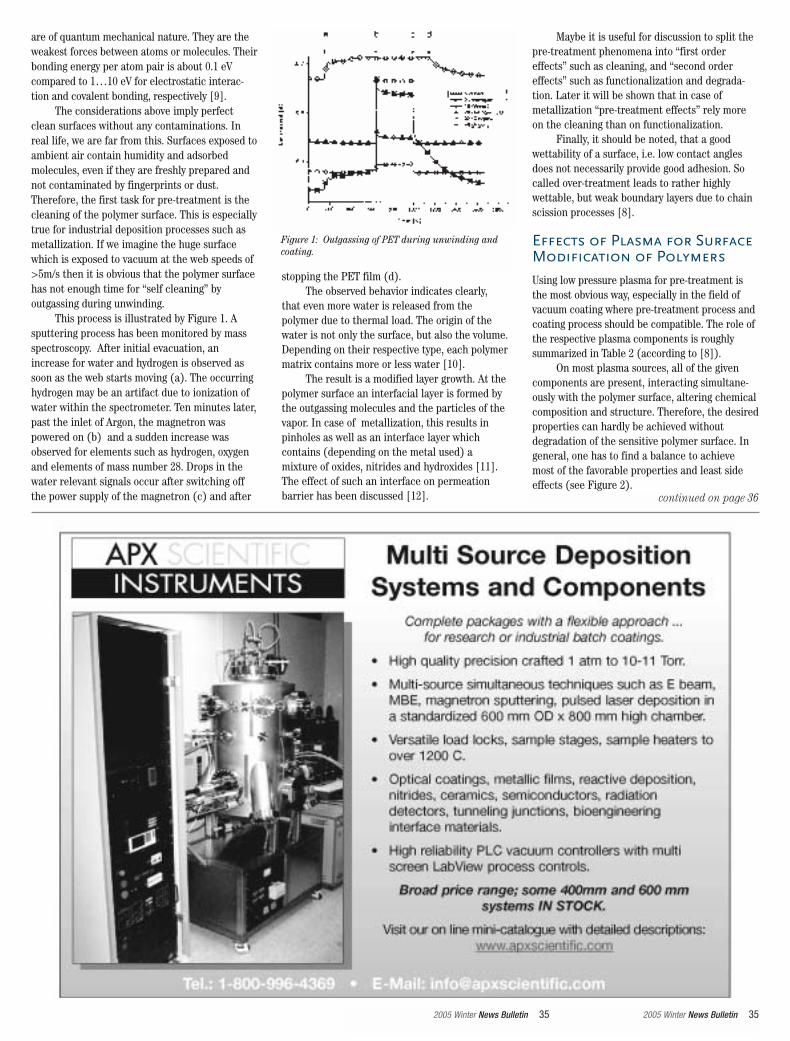
2005 Winter News Bulletin 35
are of quantum mechanical nature. They are theweakest forces between atoms or molecules. Theirbonding energy per atom pair is about 0.1 eVcompared to 1…10 eV for electrostatic interac-tion and covalent bonding, respectively [9].
The considerations above imply perfectclean surfaces without any contaminations. Inreal life, we are far from this. Surfaces exposed toambient air contain humidity and adsorbedmolecules, even if they are freshly prepared andnot contaminated by fingerprints or dust.Therefore, the first task for pre-treatment is thecleaning of the polymer surface. This is especiallytrue for industrial deposition processes such asmetallization. If we imagine the huge surfacewhich is exposed to vacuum at the web speeds of>5m/s then it is obvious that the polymer surfacehas not enough time for “self cleaning” byoutgassing during unwinding.
This process is illustrated by Figure 1. Asputtering process has been monitored by massspectroscopy. After initial evacuation, anincrease for water and hydrogen is observed assoon as the web starts moving (a). The occurringhydrogen may be an artifact due to ionization ofwater within the spectrometer. Ten minutes later,past the inlet of Argon, the magnetron waspowered on (b) and a sudden increase wasobserved for elements such as hydrogen, oxygenand elements of mass number 28. Drops in thewater relevant signals occur after switching offthe power supply of the magnetron (c) and after
stopping the PET film (d).The observed behavior indicates clearly,
that even more water is released from thepolymer due to thermal load. The origin of thewater is not only the surface, but also the volume.Depending on their respective type, each polymermatrix contains more or less water [10].
The result is a modified layer growth. At thepolymer surface an interfacial layer is formed bythe outgassing molecules and the particles of thevapor. In case of metallization, this results inpinholes as well as an interface layer whichcontains (depending on the metal used) amixture of oxides, nitrides and hydroxides [11].The effect of such an interface on permeationbarrier has been discussed [12].
Maybe it is useful for discussion to split thepre-treatment phenomena into “first ordereffects” such as cleaning, and “second ordereffects” such as functionalization and degrada-tion. Later it will be shown that in case ofmetallization “pre-treatment effects” rely moreon the cleaning than on functionalization.
Finally, it should be noted, that a goodwettability of a surface, i.e. low contact anglesdoes not necessarily provide good adhesion. Socalled over-treatment leads to rather highlywettable, but weak boundary layers due to chainscission processes [8].
Effects of Plasma for SurfaceModification of Polymers
Using low pressure plasma for pre-treatment isthe most obvious way, especially in the field ofvacuum coating where pre-treatment process andcoating process should be compatible. The role ofthe respective plasma components is roughlysummarized in Table 2 (according to [8]).
On most plasma sources, all of the givencomponents are present, interacting simultane-ously with the polymer surface, altering chemicalcomposition and structure. Therefore, the desiredproperties can hardly be achieved withoutdegradation of the sensitive polymer surface. Ingeneral, one has to find a balance to achievemost of the favorable properties and least sideeffects (see Figure 2).
2005 Winter News Bulletin 35
Figure 1: Outgassing of PET during unwinding andcoating.
continued on page 36
Plasma Sources for Pre-treatment
In the following some practical aspects for theevaluation of suitable plasma sources are given.Instead of discussing about appropriate plasmasources for evaporation or sputtering, the webspeed as a more universal criterion is used. Thevalue of 1 m/s to distinguish high-speed fromlow-speed processes is somewhat arbitrary but itis not decisive for the discussion in itself.
A) Web speed >1 m/s
This area is usually covered by industrialevaporation techniques such as metallization.Common web speeds are well above 5 m/s.Plasma sources need a sufficient high power toachieve the desired results. In this case, weneglect the second order effects and consideronly the cleaning of the polymer surface (i.e. theso-called “first order effects” mentioned above).Neglecting the individual influence of eachplasma species, we can summarize the interac-tion of plasma and polymer surface using anenergy flux density. Depending on its speed, a
moving web surface is exposed to the plasma fora time reciprocal to the web speed. It has beenfound, that a threshold of 10 mJ/cm2 value isnecessary to observe pre-treatment effects incase of metallizing biaxially orientedPolypropylene (BOPP) [2]. If one knows thepower density of a given plasma source providedto the substrate surface, then the contribution ofthe energy flux density for a given speed can beestimated easily. Knowing this, it becomes clearwhether one or more plasma sources in parallelare needed to achieve the required pre-treatment effect. Table 3 gives an overview ofpossible plasma sources and gives a first indica-tion of which plasma sources are suitable forevaporation.
This approach seems to be more relevantthan considering pure plasma parameters likecharge carrier density (commonly called plasmadensity) or ion current density, for instance.Terms such as the often cited “high densityplasma sources” can be misleading. It is difficultto conclude to the effects on the polymer surfaceat a given web speed. In that case, the energyflux density is a more practical parameter whichcan be determined for any plasma source experi-mentally [13], and the reasoning regarding thethreshold value mentioned earlier is supportedby another, completely different “pre-treatmentprocess” using laser technique [14].
The setup of the plasma source, i.e.geometric considerations, may become veryimportant. For instance, a linear rf-dischargewith a hollow anode design proofed to be veryadvantageous because the plasma is located inthe immediate vicinity of the polymer surfaceand provides a power density of about 1 W/cm2.Due to the hollow anode design, the powerabsorbed by the plasma can be delivered
Board of DirectorsPresident
Clark Bright3M [email protected]
Vice PresidentPeter MartinBattelle Pacific Northwest [email protected]
Immediate Past PresidentJohn T. FeltsNano Scale Surface Systems, [email protected]
SecretaryDavid A. GlockerIsoflux [email protected]
TreasurerMichael AndreasenVACUUM COATING Technologies, [email protected]
DirectorsHana BaránkováUppsala [email protected]
Pamela DiesingSAGE industrial sales, [email protected]
Elizabeth JosephsonApplied Films [email protected]
Traci LangevinSoleras [email protected]
Ludvik MartinuÉcole [email protected]
Paolo RaugeiGalileo Vacuum Systems, [email protected]
Ric ShimshockMLD Technologies [email protected]
Douglas SmithVacuum Process Technology, [email protected]
Frank ZimoneDenton Vacuum, [email protected]
SVC Administrative Offices71 Pinon Hill Place NEAlbuquerque, NM 87122-1914
Telephone 505/856-7188 Fax 505/856-6716E-mail [email protected] Site www.svc.org
Executive DirectorVivienne Harwood Mattox
Technical DirectorDonald M. Mattox
36 2005 Winter News Bulletin
Adhesion Promotion Techniques forCoating of Polymer Filmscontinued from page 35
Plasma Energy Effectcomponents
Electrons 1 … 8 eV Energy transfer(depending on (heating)discharge type)
Ions < 10 eV Implantation, chemical reactions,functionalization
100 eV … Sputtering (etching),some keV chain scissoring,
Implantation (“behind” the surface)
Excited < 10 eV chemical reaction,neutrals functionalization, (radicals) cross linking
Fast neutrals > 100 eV same as fast ions
Photons > 3.5 eV (UV) cracking of bonds(activating), cross linking
3.5 eV … Energy transfer1.6 eV (VIS) (heating)
< 1.6 eV (IR)
Table 2: Components of the plasma and their effect topolymer surfaces.
Type Web speed>1m/s <1m/s
Mid-frequency X X* [15]plasma source
Plasma treater X [16](Atmospheric pressuredischarge)
RF-plasma tool (Linear X X* [17]RF plasma source)
WebTreater (Magnetically X X* [2]enhanced linear RFplasma source)
Duo PlasmaLine (Linear X X [18]microwave plasma source)
Anode layer ion source X** [19,20,21]
Magnetron plasma source X This paper
*) Only if operated at low power**) Only if operated in the so called “diffuse mode”
Table 3: Possible plasma sources for pre-treatment.
Figure 2: Functionalization and degradation as afunction of pre-treatment dose.
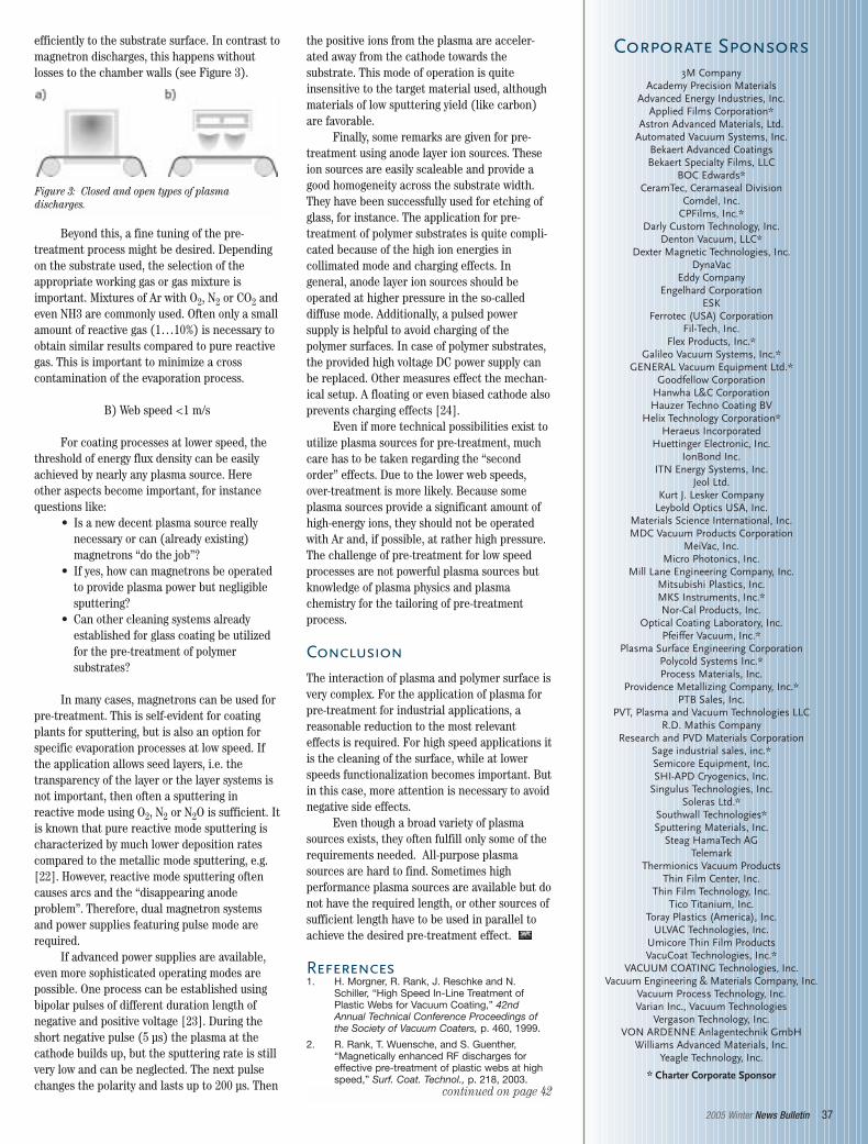
Corporate Sponsors3M Company
Academy Precision MaterialsAdvanced Energy Industries, Inc.
Applied Films Corporation*Astron Advanced Materials, Ltd.
Automated Vacuum Systems, Inc.Bekaert Advanced CoatingsBekaert Specialty Films, LLC
BOC Edwards*CeramTec, Ceramaseal Division
Comdel, Inc.CPFilms, Inc.*
Darly Custom Technology, Inc.Denton Vacuum, LLC*
Dexter Magnetic Technologies, Inc.DynaVac
Eddy CompanyEngelhard Corporation
ESKFerrotec (USA) Corporation
Fil-Tech, Inc.Flex Products, Inc.*
Galileo Vacuum Systems, Inc.*GENERAL Vacuum Equipment Ltd.*
Goodfellow CorporationHanwha L&C CorporationHauzer Techno Coating BV
Helix Technology Corporation*Heraeus Incorporated
Huettinger Electronic, Inc.IonBond Inc.
ITN Energy Systems, Inc.Jeol Ltd.
Kurt J. Lesker CompanyLeybold Optics USA, Inc.
Materials Science International, Inc.MDC Vacuum Products Corporation
MeiVac, Inc.Micro Photonics, Inc.
Mill Lane Engineering Company, Inc.Mitsubishi Plastics, Inc.MKS Instruments, Inc.*Nor-Cal Products, Inc.
Optical Coating Laboratory, Inc.Pfeiffer Vacuum, Inc.*
Plasma Surface Engineering CorporationPolycold Systems Inc.*Process Materials, Inc.
Providence Metallizing Company, Inc.*PTB Sales, Inc.
PVT, Plasma and Vacuum Technologies LLCR.D. Mathis Company
Research and PVD Materials CorporationSage industrial sales, inc.*Semicore Equipment, Inc.SHI-APD Cryogenics, Inc.
Singulus Technologies, Inc.Soleras Ltd.*
Southwall Technologies*Sputtering Materials, Inc.
Steag HamaTech AGTelemark
Thermionics Vacuum ProductsThin Film Center, Inc.
Thin Film Technology, Inc.Tico Titanium, Inc.
Toray Plastics (America), Inc.ULVAC Technologies, Inc.
Umicore Thin Film ProductsVacuCoat Technologies, Inc.*
VACUUM COATING Technologies, Inc.Vacuum Engineering & Materials Company, Inc.
Vacuum Process Technology, Inc.Varian Inc., Vacuum Technologies
Vergason Technology, Inc.VON ARDENNE Anlagentechnik GmbH
Williams Advanced Materials, Inc.Yeagle Technology, Inc.
* Charter Corporate Sponsor
2005 Winter News Bulletin 37
efficiently to the substrate surface. In contrast tomagnetron discharges, this happens withoutlosses to the chamber walls (see Figure 3).
Beyond this, a fine tuning of the pre-treatment process might be desired. Dependingon the substrate used, the selection of theappropriate working gas or gas mixture isimportant. Mixtures of Ar with O2, N2 or CO2 andeven NH3 are commonly used. Often only a smallamount of reactive gas (1…10%) is necessary toobtain similar results compared to pure reactivegas. This is important to minimize a crosscontamination of the evaporation process.
B) Web speed <1 m/s
For coating processes at lower speed, thethreshold of energy flux density can be easilyachieved by nearly any plasma source. Hereother aspects become important, for instancequestions like:
• Is a new decent plasma source reallynecessary or can (already existing)magnetrons “do the job”?
• If yes, how can magnetrons be operatedto provide plasma power but negligiblesputtering?
• Can other cleaning systems alreadyestablished for glass coating be utilizedfor the pre-treatment of polymersubstrates?
In many cases, magnetrons can be used forpre-treatment. This is self-evident for coatingplants for sputtering, but is also an option forspecific evaporation processes at low speed. Ifthe application allows seed layers, i.e. thetransparency of the layer or the layer systems isnot important, then often a sputtering inreactive mode using O2, N2 or N2O is sufficient. Itis known that pure reactive mode sputtering ischaracterized by much lower deposition ratescompared to the metallic mode sputtering, e.g.[22]. However, reactive mode sputtering oftencauses arcs and the “disappearing anodeproblem”. Therefore, dual magnetron systemsand power supplies featuring pulse mode arerequired.
If advanced power supplies are available,even more sophisticated operating modes arepossible. One process can be established usingbipolar pulses of different duration length ofnegative and positive voltage [23]. During theshort negative pulse (5 µs) the plasma at thecathode builds up, but the sputtering rate is stillvery low and can be neglected. The next pulsechanges the polarity and lasts up to 200 µs. Then
the positive ions from the plasma are acceler-ated away from the cathode towards thesubstrate. This mode of operation is quiteinsensitive to the target material used, althoughmaterials of low sputtering yield (like carbon)are favorable.
Finally, some remarks are given for pre-treatment using anode layer ion sources. Theseion sources are easily scaleable and provide agood homogeneity across the substrate width.They have been successfully used for etching ofglass, for instance. The application for pre-treatment of polymer substrates is quite compli-cated because of the high ion energies incollimated mode and charging effects. Ingeneral, anode layer ion sources should beoperated at higher pressure in the so-calleddiffuse mode. Additionally, a pulsed powersupply is helpful to avoid charging of thepolymer surfaces. In case of polymer substrates,the provided high voltage DC power supply canbe replaced. Other measures effect the mechan-ical setup. A floating or even biased cathode alsoprevents charging effects [24].
Even if more technical possibilities exist toutilize plasma sources for pre-treatment, muchcare has to be taken regarding the “secondorder” effects. Due to the lower web speeds,over-treatment is more likely. Because someplasma sources provide a significant amount ofhigh-energy ions, they should not be operatedwith Ar and, if possible, at rather high pressure.The challenge of pre-treatment for low speedprocesses are not powerful plasma sources butknowledge of plasma physics and plasmachemistry for the tailoring of pre-treatmentprocess.
Conclusion
The interaction of plasma and polymer surface isvery complex. For the application of plasma forpre-treatment for industrial applications, areasonable reduction to the most relevanteffects is required. For high speed applications itis the cleaning of the surface, while at lowerspeeds functionalization becomes important. Butin this case, more attention is necessary to avoidnegative side effects.
Even though a broad variety of plasmasources exists, they often fulfill only some of therequirements needed. All-purpose plasmasources are hard to find. Sometimes highperformance plasma sources are available but donot have the required length, or other sources ofsufficient length have to be used in parallel toachieve the desired pre-treatment effect.
References1. H. Morgner, R. Rank, J. Reschke and N.
Schiller, “High Speed In-Line Treatment ofPlastic Webs for Vacuum Coating,” 42ndAnnual Technical Conference Proceedings ofthe Society of Vacuum Coaters, p. 460, 1999.
2. R. Rank, T. Wuensche, and S. Guenther,“Magnetically enhanced RF discharges foreffective pre-treatment of plastic webs at highspeed,” Surf. Coat. Technol., p. 218, 2003.
Figure 3: Closed and open types of plasmadischarges.
continued on page 42
38 2005 Winter News Bulletin
The Society of Vacuum Coaters is pleased to announce that the followingindividuals have been elected by the SVC membership to serve three-yearterms on the SVC Board of Directors, starting at the Annual Businessmeeting at 7:00 p.m. on April 24, 2005.
• David J. Christie, Advanced Energy Industries, Inc.
• Wolfgang Decker, Toray Plastics (America), Inc.
• Vasgen Shamamian, Dow Corning Corporation
• Edward Wegener, AFG Industries (second term)
The Symposium on Functional Coatings and Surface Engineering (FCSE– 2005) will take place in Montréal, Canada on June 8–10, 2005. It ishosted by the “Regroupement québécois sur les matériaux de pointe—RQMP,” École Polytechnique, and the Université de Montréal. Symposiumtopics include: coatings for optics, optoelectronics, and imaging; coatings foraerospace and for energy control; coatings and films for micro-and nanoelec-tronics; new processes, process control, and monitoring; and characteriza-tion methods. For more information, contact the Meeting Chair LudvikMartinu ([email protected]) or the Co-Chair Jolanta Klemberg-Sapieha([email protected]), both with École Polytechnique, or go towww.unyvac.org.
The AVS Sixth International Conference on Microelectronics andInterfaces (ICMI) is to be held March 21–23, 2005, at the Santa ClaraConvention Center in Santa Clara, CA. The ICMI provides a unique opportu-nity for microelectronic process and integration specialists to gather anddiscuss challenges in fabricating nanodevices. This year’s program will
enable participants to follow three tracks of presentations, FEOLprocessing/integration, BEOL processing/integration, andmetrology/defects/yield enhancement. Each day a keynote address will coverone of these three topic tracks. For further details visit the AVS Web Site athttp://www.avs.org or call AVS West at 530/896-0477.
The Association of Vacuum Equipment Manufacturers International willhold a Spring Seminar at the Santa Clara Convention Center, CA, on themorning of March 22, 2005. The seminar titled, “The Latest Market Trends,Vacuum Techniques and Technologies,” will feature speakers from AdvancedForecasting, Lawrence Livermore National Laboratory, Hiden Analytical,Gencoa Ltd., and Stanford Research Systems. The speakers will addresscurrent topics of interest to those working in vacuum-related technologyfields. Before the seminar, network with experts at the hot buffet breakfastat 7:45 a.m.—an integral part of this program. After the seminar, visit theNorthern California Chapter AVS Annual Equipment Exhibit on theafternoon of March 22! Don’t miss this unique opportunity to gain knowledgeyou can use from experts in several vacuum equipment market segments.For registration and further information, visitwww.avem.org/Seminar/index.html or send an e-mail to [email protected].
The next offering of the Distance Learning Self-Paced Course onFundamentals of Vapor Deposition (which is sponsored by SVC in collabo-ration with the University of Delaware) will be June 13–24, 2005. Theflexibility of self-paced study allows students to work whenever and whereverthey want, with the availability of the instructor through a web-based portalestablished at the University of Delaware. If you want more information,please contact SVC at 505/856-7188, or by E-mail at [email protected].
Society and Industry News
The Association ofVacuum Equipment
ManufacturersInternational invites you
to a Seminar on
Your Invitation to Learn!At this AVEM International Seminar, speakers will address current topics ofinterest to those working in vacuum-related technology fields. Before theSeminar, network with experts at the hot buffet breakfast starting at 7:45 a.m. –an integral part of this program. After the Seminar, visit the Northern CaliforniaChapter AVS Annual Equipment Exhibit on the afternoon of March 22!
March 22, 20058:30 a.m.–11:45 a.m.
(Breakfast at 7:45 a.m.)
Santa Clara ConventionCenter, Santa Clara, CA
Seminar held during the AVSSixth International Conference
on Microelectronics andInterfaces (ICMI)
Visit www.avem.org to download the registration form and make your hotel andtravel arrangements. For additional seminar information, contact:
Association of Vacuum Equipment Manufacturers International505/856-6924 • Fax 505/856-6716
E-mail <[email protected]> • Web Site <www.avem.org>
Topics include:" An Overview of Applications of Vacuum Technology Required for the World’s Most
Powerful Laser System - NIF with Peter Biltoft, Lawrence Livermore National Laboratory" Forecast of the Next Turning-Point in Demand for Equipment Components
with Moshe Handelsman and Rosa Luis, Advanced Forecasting" State of the Art and Industry Demands for Magnetron Sputter Technologies
with Dermot Monaghan, Gencoa Ltd." What Makes a Vacuum Product Successful? with Gerardo A. Brucker, Stanford Research
Systems, Inc." Quadrupole Mass Spectrometry Applications in Residual Gas Analysis and
Production Control for Semiconductor Processing and Fabrication with Mark Buckley,Hiden Analytical Inc.
The Latest Market Trends, VacuumTechniques and Technologies
2005 Winter News Bulletin 39
Corporate Sponsor News
On December 1, 2004, Bodycote Plc. and Stirling Square Capital Partners(SSCP) concluded an agreement, whereby the PVD coating activities of Bodycotewere acquired by SSCP. SSCP is also a majority shareholder of the IonBondGroup. The two groups will be merged into one new group, called IonBond. Inthe Netherlands the name of Bodycote Coating Centrum BV will be changed toIonBond Netherlands BV. The new group, IonBond, will combine thecompetences of the former Bodycote PVD group and the IonBond Group. Thecombined global sales volume of 80 M Euros assures that the “new” IonBondGroup is the second largest provider of PVD and PACVD coating services in theworld.
CeramTec North America has been certified as fully compliant with the stringentnew ISO/TS 16949:2002 quality standard. The recognition came after an extendedeffort by CeramTec staff and exhaustive review of company processes by anindependent third-party auditor. Successor to QS-9000 guidelines, the TS16949:2002 standard provides a single quality management system. The standardhas quickly won acceptance and support from automotive suppliers and manufac-turers around the world, including GM, Ford, and DaimlerChrysler in the U.S. Inannouncing the certification, Walt Dollman, CeramTec North America Presidentand CEO, thanked his colleagues for their dedication in achieving the verydifficult process-oriented standard. CeramTec already supplies a wide range ofhigh-strength, ceramic-based sensors and electronic insulators to the globalautomotive industry. The new requirement establishes a stricter level ofdocumentation, process efficiency, quality control, customer focus, planning,training, and auditing than earlier standards.
Comdel, Inc., is making a long-term commitment to customers in Japan byopening a branch office in Chiba, Japan. At the same time they entered into astrategic agreement with PRA Co. Ltd., a local service and repair company, toexpand Comdel’s capabilities in the region. These actions were taken in an effortto better serve customers in Japan by improving equipment uptime and helpingmanage costs.
Denton Vacuum LLC announces the recent addition of Rod Moore to theexecutive team as Director of Technology and Strategic Development. Rod bringsconsiderable experience to the organization with thin film experience gainedworking for organizations such as Corning, Essilor, TetraPak, and the U.S. Army.Rod Moore has worked with ophthalmic and precision optical products, havingdeveloped new coating designs and re-engineered processes to establish stablemanufacturing parameters for volume production.
Ceradyne, Inc. (NASDAQ:CRDN) announces the acquisition of ESK from itsprevious parent, Wacker-Chemie, a German silicon and chemical manufacturer.ESK was started in 1922 to produce non-oxide powders and technical ceramics.The company, then known as Electroschmelzwerk Kempten AG, was acquired byWacker-Chemie GmbH in 1933 and has operated under the name WackerCeramics since 2001. Ceradyne intends to revert back to the original ESK name.The company’s major product lines include its worldwide position as a primesupplier of boron carbide powder, which is the starting material for much ofCeradyne’s lightweight ceramic armor that accounts for over 60% of Ceradyne’ssales. ESK is considered a world leader in several industrial categories ofadvanced technical ceramics, accounting for over 90% of its sales, includingevaporation boats for the vacuum metallizing process. Ceradyne develops,manufactures, and markets advanced technical ceramic products andcomponents. Additional information about the company can be found atwww.ceradyne.com. ESK customers can continue to refer any questions orcomments to their existing sales and technical contacts.
Goodfellow Corporation of Devon, PA, and an international supplier of high-purity metals and materials, recently learned from the British National SpaceCentre that platinum wire, gold, and other high-purity metals it supplied almost adecade ago are part of the Cassini-Huygens spacecraft that has been orbiting theringed planet of Saturn after a seven-year journey from Earth. On December 24,
continued on page 40
40 2005 Winter News Bulletin
the Huygens probe section of the spacecraftbegan its historic descent to Titan, the largest ofSaturn’s 33 moons. The Cassini-Huygensspacecraft is made up of the Cassini orbiter,developed by NASA, and the Huygens probe,developed by the European Space Agency. TheItalian Space Agency provided the high-gainantenna, much of the radio system, and several ofCassini’s instruments. Cassini entered Saturn’sorbit on July 1 of 2004 and conducted in-depth
studies of the planet, its moons, rings, andmagnetic environment. On December 24, Cassinidispatched the 9-foot-diameter Huygens probe toTitan. The probe is scheduled to reach theatmosphere of Titan on January 14 and continueits descent to the moon’s surface. Huygens is thefirst probe to land on a world in the outer SolarSystem, and it is in Huygens that the instrumentsmade from Goodfellow’s metals are housed. Oneof the scientific components being used in theexploration is the THP sensor, an instrument thatmeasures thermal conductivity and thermaldiffusivity by means of platinum wires suppliedby Goodfellow. The sensor will transmit datarelative to the temperature and thermal conduc-tivity of the surface and lower atmosphere ofTitan and the heat capacity of the surfacematerial. The Cassini-Huygens mission is amodel of international scientific cooperation,with thousands of academic and industrial partic-ipants worldwide. The project is one of the mostambitious and challenging interplanetaryexplorations ever mounted.
IGC Polycold Systems Inc., a division ofIntermagnetics General Corporation (NASDQ:IMGC), recognized its 30th anniversary onOctober 14, 2004, and celebrated 30 years ofquality, reliability, and innovation. Polycolddesigns, manufactures, and sells a variety of
specialized cryogenic refrigeration equipmentused in numerous high tech, industrial, scientific,and biomedical applications. Productsdepending upon Polycold technology range fromthe everyday, such as eyeglasses and snack bags,consumer electronics such as cellular phones,digital cameras and flat screen televisions—tothe extraordinary, such as baggage scanners forhomeland security, drug discovery screeningdevices, to telescopes and precision scientificinstruments.
MKS Instruments, Inc. (NASDAQ: MKSI), aleading provider of process control technologiesfor improving productivity in semiconductor andother advanced manufacturing process environ-ments, has relocated MKS’ two Austin, TX, sitesinto one larger facility. The consolidation bringstogether MKS Austin Sales & Field Service,product development for Control & InformationTechnology Products, and R&D/product develop-ment for Power & Reactive Gas Products into one20,880-square-foot facility that has beenorganized and facilitated to better meet MKS’business goals. The larger facility, whichincludes a new lab to provide hands-on producttraining to customers, enhances communicationand interaction among the various MKS productgroups, allowing MKS to more efficiently meetthe needs of its customers.
Corporate Sponsor Newscontinued from page 39
Registering for the TechCon doesn’tget any easier than this!
Register on-line at www.svc.org
Corporate Sponsor Profile
Vacuum Coating Technnologies, Inc.
In April 2002, the glass coater business of BOC Coating Technologywas acquired by VON ARDENNE Anlagentechnik GmbH and renamedVON ARDENNE Coating Technology, Inc. (VACT). With this acquisi-tion, VON ARDENNE became a leading supplier of coating equipmentto the glass industry based on the market leading position of BOCCoating Technology.
An investment group, led by the management of VON ARDENNECoating Technology, located in Fairfield, CA, recently purchased thecompany from VON ARDENNE Anlagentechnik GmbH, Germany.VON ARDENNE Coating Technology, Inc., operating under the newname VACUUM COATING Technologies, Inc. (VACT), will continue tooperate as a leading manufacturer and supplier of technologicallyadvanced turnkey sputter coating systems and state-of-the-artcomponents for production of low-emissivity and solar control glass forarchitectural and automotive applications. In addition, VACT will alsocontinue to supply coating systems for production of antireflectivecoatings for display applications as well as for the photovoltaic industryin production of thin film solar cells in the same Fairfield, CA, location.
VACUUM COATING Technologies, Inc., (formerly BOC CoatingTechnology) has the largest installed base of glass coaters worldwidewith equipment operating in more than 40 countries. Although thename has changed, a number of times throughout the history of theircompany, their focus and team have remained extremely stable.
BOC Coating Technology
VON ARDENNE Coating Technology Inc. (VACT)
VACUUM COATING Technologies, Inc. (VACT)
VACUUM COATING Technologies, Inc. benefits from and relies on anumber of firsts accomplished by the company under formerownerships such as:
• First sputtered glass automobile product 1975
• First architectural glass coater to go online 1977
• First silver-based low emissivity coater 1983
• Cylindrical sputtering cathode (C-MAG®) introduced 1989
• Medium frequency AC C-MAG® system for reactive sputteringintroduced 1998
VACUUM COATING Technologies, Inc. will continue existing develop-ment programs leading to the introduction of new products andcapabilities. They retain all rights to their current technologies,including our proprietary C-MAG cylindrical magnetron, VAC-MAG™endblock design and AC technology. In addition to developing new andflexible coater designs, the company will continue to manufacture andsell diffusion pump based modular coating systems. The latestadvances to the coaters includes the use of patented end-blockscapable of accepting up to 400 Amps AC for the C-MAG® sources,target designs that allow over 90% utilization, and designs for high-speed cycle times.
VACUUM COATING Technologies, Inc. continues to be a source ofcoating equipment and technology products for the glass industry withoffices in China and Europe in support of its current installed base andfor future business in those areas in addition to its headquarters in theUSA. For more information contact: Agnes Chow 707-423 2143; E-mail:[email protected].

Turbo pump
Leading the way in the glass coating industryfor more than 25 years.
Diffusion pump
USA HeadquartersVACUUM COATING Technologies, Inc.2700 Maxwell Way, Fairfield, CA 94534 USATel: +1-707-423-2100 Fax: +1-707-425-6071E-mail: [email protected] website: www.vact.com
AsiaVACUUM COATING Technologies (Shanghai) Co., Ltd.188 Zhangyang Rd., Tomson Center, Suite B1303Pudong, Shanghai 200120, ChinaTel: +86 21 5876 2900 Fax: +86 21 5879 8103
EuropeVACUUM COATING Technologies GmbHGlashütter Straße 101aD-01277 Dresden, GermanyTel: +49 351 205 86-0 Fax: +49 351 205 86-10
Visit us at the2005 SVC TechCon Exhibit
April 25–26, 2005Denver, CO
Introducing the flexible VAC™ 870Compartment Coating System.
Introducing the flexible VAC™ 870Compartment Coating System.
Giving you choices.Giving you choices.
42 2005 Winter News Bulletin
Advertiser’s Index
ConclusionThese are just some examples of simple optical coatings. They are
typical of some of the building blocks that are used as the startingstructures for more complex and higher-performance designs. For examplethe designs of Dense Wavelength Division Multiplexing Filters follow thekinds of structures used in Figure 7 but frequently have around 200 layersrather than the 44 or so shown. Because the structures are so complicatedand accurate calculations are so involved and tedious, computers areindispensable in coating design.
Further ReadingThere are many books dealing with thin-film optical coatings. Three
recent ones, still in print, are:
Kaiser, N and H K Pulker, eds. Optical Interference Coatings. OpticalSciences, ed. W.T. Rhodes. 2003, Springer-Verlag: Berlin, Heidelberg,New York. pp 500.
Macleod, H A, Thin-Film Optical Filters. Third ed. 2001, Bristol andPhiladelphia: Institute of Physics Publishing.
Willey, Ronald R, Practical Design and Production of Optical ThinFilms. Second ed. Optical Engineering, ed. B. Thompson. 2002, NewYork, Basel: Marcel Dekker Inc.
Fundamentals of Optical Coatingscontinued from page 32
Adhesion Promotion Techniques forCoating of Polymer Filmscontinued from page 37
3. A. Yializis, M.G. Mikhael, R.E. Ellwanger, and E.M. Mount III, “SurfaceFunctionalization of Polymer Films“, 42nd Annual Technical ConferenceProceedings of the Society of Vacuum Coaters, p. 469, 1999.
4. A. Yializis, M.G. Mikhael, T.A. Miller, and R.E. Ellwanger, “Use of FunctionalAcrylate Polymers for Different Web Coating Applications,” Proc. 11th Int.Conf. on Vacuum Web Coating, p. 138, 1997.
5. P. Grπning, O.M. Kuttel, M. Collaud-Coen, G. Dietler, and L. Schlapbach,“Interaction of low-energy ions (<10 eV) with polymethylmethacrylate duringplasma treatment,” Appl. Surf. Sci. 89(1), p. 83, 1995.
6. F. Garbassi, M. Morra, E. Occhiello, L. Barino, and R. Scordamaglia,“Dynamics of macromolecules: a challenge for surface analysis,” Surf. Interf.Anal. 14(10), p.585, 1989.
7. R.W. Burger and L.J. Gerenser, “Understanding the Formation and Propertiesof Metal/Polymer Interfaces via Spectroscopic Studies of Chemical Bonding,”34th Annual Technical Conference Proceedings of the Society of VacuumCoaters, p. 162, 1991.
8. F.D. Egitto and L.J. Matienzo, “Plasma modification of polymer surfaces foradhesion improvement,” IBM J. Res. Dev. 38(4), p. 423, 1994.
9. B. Chapman, “Thin Film adhesion,” J. Vac. Sci. Technol., 11(1), p. 106, 1974.
10. M. Roehrig and C. Bright, “Vacuum Heat Transfer Models for WebSubstrates: Review of Theory and Experimental Heat Transfer Data,” 43rdAnnual Technical Conference Proceedings of the Society of Vacuum Coaters,p. 335, 2000.
11. A. Yializis, R.E. Ellwanger, and J. Harvey, “Barrier Degradation in AluminumMetallized Polypropylene Films,” 40th Annual Technical ConferenceProceedings of the Society of Vacuum Coaters, p. 371, 1997.
12. W. Decker and B. Henry, “Basic Principles of Thin Film Barrier Coatings,”45th Annual Technical Conference Proceedings of the Society of VacuumCoaters, p. 492, 2002.
13. H. Kersten, R. Wiese, D. Gorbov, A. Kapitov, F. Scholze, and H. Neumann,“Characterization of a broad beam ion source by determination of the energyflux,” Surf. Coat. Technol. 173-174, p. 918, 2003.
14. D.J. McClure, D.S. Dunn, and A.J. Ouderkirk, “Adhesion PromotionTechnique for Coatings on PET, PEN and PI,” 43rd Annual TechnicalConference Proceedings of the Society of Vacuum Coaters, p. 342, 2000.
15. V. Cassio, “Plasma Pre-Treatment in Aluminum Web Coating: A ConverterExperience,” 42nd Annual Technical Conference Proceedings of the Societyof Vacuum Coaters, p. 465, 1999.
16. S.A. Pirzada, A. Yializis, W. Decker, and R.E. Ellwanger, “Plasma Treatment ofPolymer Films,” 42nd Annual Technical Conference Proceedings of theSociety of Vacuum Coaters, p. 301, 1999.
17. M. Geisler, J. Bartella, G. Hoffmann, R. Kukla, R. Ludwig, and D. Wagner, “rfPlasma Tool for Ion-Assisted Large-Scale Web and Sheet Processing,” 44thAnnual Technical Conference Proceedings of the Society of Vacuum Coaters,p. 482, 2001.
18. R. Emmerich, M. Kaiser, H. Urban, M. Graf, E. Rauchle, P. Elsner, J.Feichtinger, A. Schulz, M. Walker, K.M. Baumgartner, and H. Muegge, “Newmicrowave plasma sources for large scale applications up to atmosphericpressure,” Proc. IEEE 29th Int. Conf. on Plasma Sciences, p. 320, 2002.
19. I.V. Svadkovski and A.P. Dostanko, “Ion sources for ion beam assisted thinfilm deposition,” Symposium Ion-Solid Interactions for Materials Modificationand Processing, p. 635, 1996.
20. A. Shabalin, M. Amann, M. Kishinevsky, K. Nauman, and C. Quinn, “IndustrialIon Sources and Their Application for DLC Coating,” 42nd Annual TechnicalConference Proceedings of the Society of Vacuum Coaters, p. 338, 1999.
21. D. Burtner, R. Blacker, J. Keem, D. Siegfried, and E. Wahlin, “Linear Anode-Layer Ion Sources with 340- and 1500-mm Beams,” 46th Annual TechnicalConference Proceedings of the Society of Vacuum Coaters, p. 263, 2003.
22. S. Schiller, U. Heisig, Chr. Korndörfer, and J. Strümpfel, “Stabilization of theReactive Magnetron Discharge with Close Target-to-Substrate Coupling,”Proc. 3rd Int. Conf. on Vacuum Web Coating, p. 155, 1989.
23. Patent No.: EP 0867 036 B1.24. T. Linz (Advanced Energy Industries GmbH), private communication.
A&N Corporation . . . . . . . . . . . . . . . . . . . . . . . . . . . . . . . . . . . . . . . . . . . . . 6Ametek, Inc.. . . . . . . . . . . . . . . . . . . . . . . . . . . . . . . . . . . . . . . . . . . . . . . . 12APX Scientific Instruments, Inc. . . . . . . . . . . . . . . . . . . . . . . . . . . . . . . . 35AVEM International . . . . . . . . . . . . . . . . . . . . . . . . . . . . . . . . . . . . . . . . . . 38C&C General, LLC . . . . . . . . . . . . . . . . . . . . . . . . . . . . . . . . . . . . . . . . . . . 21Coating 2005 . . . . . . . . . . . . . . . . . . . . . . . . . . . . . . . . . . . . . . . . . . . . . . . 33Comdel, Inc. . . . . . . . . . . . . . . . . . . . . . . . . . . . . . . . . . . . . . . . . . . . . . . . . 10Denton Vacuum, LLC. . . . . . . . . . . . . . . . . . . . . . . . . . . . . . . . . . . . . . . . . . 3Ferrotec (USA) Corporation . . . . . . . . . . . . . . . . . . . . . . . . . . . . . . . . . . . 18Fil-Tech, Inc. . . . . . . . . . . . . . . . . . . . . . . . . . . . . . . . . . . . . . . . . . . . . . . . 14Filmetrics, Inc. . . . . . . . . . . . . . . . . . . . . . . . . . . . . . . . . . . . . . . . . . . . . . . 7Huettinger Electronic, Inc. . . . . . . . . . . . . . . . . . . . . . . . . . . . . . . . . . . . . 19Inficon . . . . . . . . . . . . . . . . . . . . . . . . . . . . . . . . . . . . . . . . . . . . . . . . . . . . 11Intelvac . . . . . . . . . . . . . . . . . . . . . . . . . . . . . . . . . . . . . . . . . . . . . . . . . . . 16ISSP 2005 . . . . . . . . . . . . . . . . . . . . . . . . . . . . . . . . . . . . . . . . . . . . . . . . . . 29Maxtek, Inc. . . . . . . . . . . . . . . . . . . . . . . . . . . . . . . . . . . . . . . . . . . . . . . . . . 9MDC Vacuum Products Corporation . . . . . . . . . . . . . . . . . . . . . . . . 22 & 23MKS Instruments, Inc. . . . . . . . . . . . . . . . . . . . . . . . . . . . . . . . . . . . . . . . 39Normandale Community College . . . . . . . . . . . . . . . . . . . . . . . . . . . . . . . 29Pacific Nanotechnology . . . . . . . . . . . . . . . . . . . . . . . . . . . . . . . . . . . . . . . 12Pfeiffer Vacuum . . . . . . . . . . . . . . . . . . . . . . . . . . . . . . . . . . . . . . . . . . . . . 17PHPK Technologies . . . . . . . . . . . . . . . . . . . . . . . . . . . . . . . . . . . . . . . . . . 15Polycold Systems, Inc. . . . . . . . . . . . . . . . . . . . . . . . . . . . . . . . . . . . . . . . . . 2R.D. Mathis Company . . . . . . . . . . . . . . . . . . . . . . . . . . . . . . . . . . . . . . . . . 5Society of Vacuum Coaters . . . . . . . . . . . . . . . . . . . . . . . . . . . . . . . . . . . . 30System Control Technologies . . . . . . . . . . . . . . . . . . . . . . . . . . . . . . . . . . 44Telemark . . . . . . . . . . . . . . . . . . . . . . . . . . . . . . . . . . . . . . . . . . . . . . . . . . 43Torr International, Inc. . . . . . . . . . . . . . . . . . . . . . . . . . . . . . . . . . . . . . . . 18ULVAC Technologies, Inc. . . . . . . . . . . . . . . . . . . . . . . . . . . . . . . . . . . . . . 34VACUUM COATING Technologies, Inc. . . . . . . . . . . . . . . . . . . . . . . . . . . . 41Vacuum Research Limited . . . . . . . . . . . . . . . . . . . . . . . . . . . . . . . . . . . . . 8Varian Inc. Vacuum Technologies . . . . . . . . . . . . . . . . . . . . . . . . . . . . . . . 27VAT, Inc. . . . . . . . . . . . . . . . . . . . . . . . . . . . . . . . . . . . . . . . . . . . . . . . . . . . 16
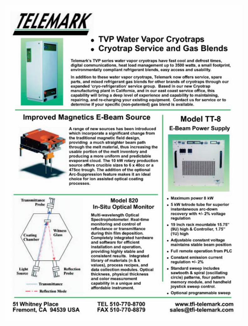
Society of Vacuum Coaters71 Pinon Hill Place NEAlbuquerque, NM 87122-1914 USA
CHANGE SERVICE REQUESTED
PRESORTED
STANDARD
US POSTAGE PAID
ALBUQUERQUE, NM
PERMIT NO 1893
It’s Not Too Late to Join the Exhibit and InnovatorsShowcase at the 2005 TechCon!April 25th and 26th at the Adam’s Mark Hotel, Denver, ColoradoThis two day, one-of-a-kind forum during the annual TechCon offers exhibitors an excellent opportunity toshowcase their latest innovations in vacuum coating and related technologies. Exhibitors will becomemore visible to prospective customers at the TechCon by participating in the Innovators Showcase—a 10-minute presentation about new products, new equipment, or a new process. Deadline for abstracts isFebruary 15 for the Innovators Showcase and booths are still available. Call 505/856-7188; E-mail:[email protected] or visit www.svc.org for more information.
PRESORTED
FIRST CLASS
US POSTAGE PAID
ALBUQUERQUE, NM
PERMIT NO 1893
Phot
o co
urte
sy o
f the
Den
ver
Met
ro C
VB
Recommended