Embed Size (px)
Citation preview

Zynq UltraScale+ MPSoC Product Tables and Product Selection Guide

© Copyright 2015 Xilinx.
Page 1
Zynq® UltraScale+™ MPSoCs
Notes:
1. For full part number details, see the Ordering Information section in DS890, UltraScale Architecture and Product Overview.
2.-2LE (Tj = 0°C to 110°C).
Disclaimer: This document contains preliminary information and is subject to change without notice. Information provided herein relates to products and/or services not yet available for sale, and provided solely for information purposes and are not intended,
or to be construed, as an offer for sale or an attempted commercialization of the products and/or services referred to herein. Please contact your Xilinx representative for the latest information.
Smarter Control and Vision Smarter Network
Device Name(1) ZU2EG ZU3EG ZU4EV ZU5EV ZU7EV ZU6EG ZU9EG ZU15EG ZU11EG ZU17EG ZU19EG
Pro
cess
ing
Syst
em
(P
S)
Application Processor Unit
Processor Core Quad-core ARM® Cortex™-A53 MPCore™ up to 1.5GHzMemory w/ECC L1 Cache 32KB I / D per core, L2 Cache 1MB, on-chip Memory 256KB
Real-Time Processor Unit
Processor Core Dual-core ARM Cortex-R5 MPCore™ up to 600MHzMemory w/ECC L1 Cache 32KB I / D per core, Tightly Coupled Memory 128KB
Graphic & Video Acceleration
Graphics Processing Unit Mali™-400MP up to 667MHzMemory L2 Cache 64KB
External MemoryDynamic Memory Interface x32/x64: DDR4, LPDDR4, DDR3, DDR3L, LPDDR3
Static Memory Interfaces NAND, 2x Quad-SPI
ConnectivityHigh-Speed Connectivity PCIe® Gen2 x4, 2x USB3.0, SATA 3.0, DisplayPort, 4x Tri-mode Gigabit Ethernet
General Connectivity 2xUSB 2.0, 2x SD/SDIO, 2x UART, 2x CAN 2.0B, 2x I2C, 2x SPI, 4x 32b GPIO
Integrated Block Functionality
Power Management Full / Low / PL / Battery Power Domains
SecurityAMS - System Monitor
RSA, AES, and SHA10-bit, 1MSPS - Temperature, Voltage, and Current Monitor
PS to PL Interface 11x 32/64/128b & 1x 32/64b AXI Ports
Pro
gram
mab
le L
ogi
c (P
L)
Programmable Functionality
System Logic Cells (K) 103 154 192 256 504 469 600 747 653 926 1,143CLB Flip-Flops (K) 94 141 176 234 461 429 548 682 597 847 1,045
MemoryMax. Distributed RAM (Mb) 1.2 1.8 2.8 3.8 6.2 6.9 8.8 11.3 9.1 8.0 9.8
Total Block RAM (Mb) 5.3 7.6 4.5 5.1 11.0 25.1 32.1 26.2 21.1 28.0 34.6UltraRAM (Mb) - - 14.0 18.0 27.0 - - 31.5 22.5 28.7 36.0
Integrated IP
DSP Slices 240 360 728 1,056 1,728 1,973 2,520 3,528 2,928 1,590 1,968Video Codec Unit (VCU) - - 1 1 1 - - - - - -
PCI Express® Gen 3x16 / Gen4x8 - - 2 2 2 - - - 4 4 5150G Interlaken - - - - - - - - 2 2 4
100G Ethernet MAC/PCS w/RS-FEC - - - - - - - - 1 2 4AMS - System Monitor 1 1 1 1 1 1 1 1 1 1 1
Speed GradesExtended(2) -1 -2L -3 -1 -2L -3
Industrial -1 -1L -2 -1 -1L -2

© Copyright 2015 Xilinx.
Notes:
1. PS I/O is a combination of PS MIO and PS DDRIO.
2. For full part number details, see the Ordering Information section in DS890, UltraScale Architecture and Product Overview.
3. These packages are only offered in 0.8mm ballpitch. All other packages are offered in 1.0mm ball pitch.
Page 2
Zynq® UltraScale+™ MPSoCsPS I/Os(1), 3.3V High-Density (HD) I/O, 1.8V High-Performance (HP) I/OsPS-GTR 6Gb/s, GTH 16.3Gb/s, GTY 32.75Gb/s
PkgFootprint(2)
Dimensions(mm)
Smarter Control and Vision Smarter Network
ZU2EG ZU3EG ZU4EV ZU5EV ZU7EV ZU6EG ZU9EG ZU15EG ZU11EG ZU17EG ZU19EG
A484(3) 19x19169, 24, 52
4, 0, 0169, 24, 52
4, 0, 0
A625(3) 21x21169, 24, 156
4, 0, 0169, 24, 156
4, 0, 0
C784(3) 23x23214, 96, 156
4, 0, 0214, 96, 156
4, 0, 0214, 96, 156
4, 4, 0214, 96, 156
4, 4, 0
B900 31x31214, 48, 156
4, 16, 0214, 48, 156
4, 16, 0214, 48, 156
4, 16, 0
C900 31x31214, 48, 156
4, 16, 0214, 48, 156
4, 16, 0214, 48, 156
4, 16, 0
B1156 35x35214, 120, 208
4, 24, 0214, 120, 208
4, 24, 0214, 120, 208
4, 24, 0
C1156 35x35214, 48, 312
4, 24, 0214, 48, 312
4, 24, 0
B1517 40x40214, 72, 416
4, 16, 0214, 72, 572
4, 16, 0214, 72, 572
4, 16, 0
F1517 40x40214, 48, 416
4, 24, 0214, 48, 416
4, 32, 0
C1760 42.5x42.5214, 96, 416
4, 32, 16214, 96, 416
4, 32, 16214, 96, 416
4, 32, 16
D1760 42.5x42.5214, 48, 260
4, 44, 28214, 48, 260
4, 44, 28
E1924 45x45214, 96, 572
4, 44, 0214, 96, 572
4, 44, 0
Important: Verify all data in this document with the device data sheets found at www.xilinx.com

© Copyright 2015 Xilinx.
Page 3
Zynq® UltraScale+™ MPSoC Ordering Information
E = Extended (Tj = 0°C to +100°C)I = Industrial (Tj = –40°C to +100°C)
Note: -L2E (Tj = 0°C to +110°C). Refer to DS890, UltraScale Product Overview for additional information.
Important: Verify all data in this document with the device data sheets found at www.xilinx.com
Xilinx Commercial
UltraScaleZynq F: LidB: Lidless
ValueIndex
F: Flip-chipw/ 1.0mmBall PitchS: Flip-chipw/ 0.8mm Ball Pitch
V: RoHS 6/6 PackageDesignator
Speed Grade-1: Slowest-L1: Low Power-2: Mid -L2: Low Power-3: Fastest
Footprint
Temperature Grade(E, I)
PackagePin Count
XC Z U # -1 F F V A # E
ProcessorSystemIdentifierE: Quad APU
Dual RPUSingle GPU
E
Engine TypeG: General PurposeV: Video
G
XMP104 (v1.4)

© Copyright 2015 Xilinx.
Page 4
MemoryZynq® UltraScale+™ MPSoCs include block RAM and UltraRAM (high density, dual-port, synchronous memory block), which increase performance, device utilization, and power efficiency. These new features are designed to provide highly efficient solutions for applications that require heterogeneous processing.
Important: Verify all data in this document with the device data sheets found at www.xilinx.com
5.3ZU2EG
ZU19EG 34.6 36.0
ZU17EG 28.728.0
26.2ZU15EG 31.5
ZU11EG 21.1 22.5
ZU9EG 32.1
ZU3EG 7.6
Total Memory (Mb) Block RAM UltraRAM
ZU6EG 25.1
11.0ZU7EV 27.0
ZU4EV 4.5 14.0
ZU5EV 5.1 18.0

© Copyright 2015 Xilinx.
Page 5
Transceiver Count and BandwidthUltraScale™ architecture serial transceivers include the proven on-chip circuits required to provide optimal signal integrity in real world environments, at data rates up to 6.0Gb/s (PS-GTR), 16.3Gb/s (GTH), and 32.75Gb/s (GTY).
Important: Verify all data in this document with the device data sheets found at www.xilinx.com
Total Transceiver Count and Bandwidth GTH GTY
PS-GTR = 6.0Gb/sGTH = 16.3Gb/sGTY = 32.75Gb/s
4ZU2EG
ZU3EG 4
PS-GTR
ZU4EV 4 16
ZU5EV 164
ZU6EG 244
16ZU11EG 324
24ZU15EG 4
ZU17EG 28444
ZU7EV 244
ZU9EG 244
ZU19EG 4 2844
24.0Gb/s
24.0Gb/s
224Gb/s
224Gb/s
415.2Gb/s
415.2Gb/s
415.2Gb/s
415.2Gb/s
1069.6Gb/s
1658.2Gb/s
1658.2Gb/s
© Copyright 2015 Xilinx.
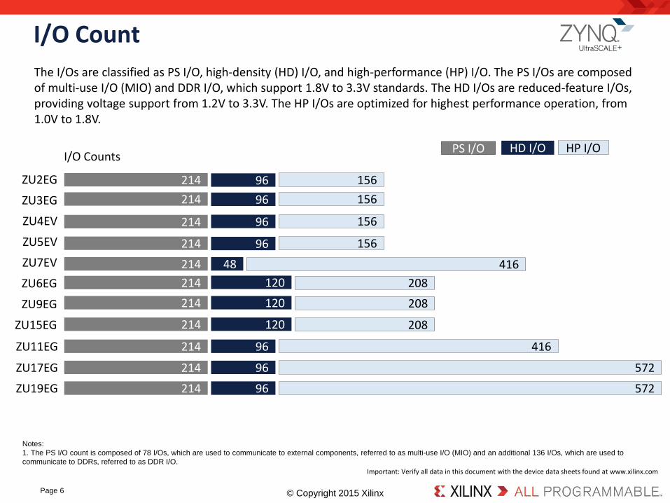
I/O Count
Page 6
Important: Verify all data in this document with the device data sheets found at www.xilinx.com
I/O Counts
208ZU15EG
ZU5EV
ZU6EG
ZU4EV
ZU7EV 416
ZU9EG
ZU3EG
ZU2EG
The I/Os are classified as PS I/O, high-density (HD) I/O, and high-performance (HP) I/O. The PS I/Os are composed of multi-use I/O (MIO) and DDR I/O, which support 1.8V to 3.3V standards. The HD I/Os are reduced-feature I/Os, providing voltage support from 1.2V to 3.3V. The HP I/Os are optimized for highest performance operation, from 1.0V to 1.8V.
416ZU11EG
572ZU19EG 96214
57296214ZU17EG
96214
214
214
214
214
214
214
214
214
120
208120
208120
48
96 156
96 156
96 156
96 156
HD I/O HP I/OPS I/O
Notes:
1. The PS I/O count is composed of 78 I/Os, which are used to communicate to external components, referred to as multi-use I/O (MIO) and an additional 136 I/Os, which are used to
communicate to DDRs, referred to as DDR I/O.