Embed Size (px)
Citation preview


SERVICING MANUAL
FOR
ZX M I C R O D R I V E , INTERFACE 1 AND INTERFACE 2
LIST OF CONTENTS -
SECTION 1 SYSTEM D E S C R I P T I O N
SECTION 2 DISASSEMBLY ASSEMBLY
SECTION 3 SETTING UP AND SYSTEM TEST
SECTION 4 FAULT DIAGNOSIS AND REPAIR
SECTION 5 PARTS LIST
- L I S T OF ILLUSTRATIONS
Fig No.
ZX Interface 1 - Block Diagram 1.1- Circui t D i a g r a m 1.2
ZX Microdrive - Circuit Diag ram 1.3
ZX Interface 2 - Circui t Diagram 1.4
ZX Microdrive - Head Chass is Mechanical Layout 4.1ZX Interface 1 - PCB Layout 5.1
ZX Microdrive - Base Board Layout 5.2
- Head Board Layout 5.3
Prepared by THORN ( E M I ) DATATECH LTD_for SINCLAIR RESEARCH LTD OCTOBER 1985
§ Sinclair Research Ltd

SECTION 1
SYSTEM DESCRIPTION
Sub-Section LIST OF CONTENTS Page No.
1 ZX Interface 1 1.1
2 ZX Microdrive 1.5
3 ZX Interface 2 1.8
4 Power Supply 1.9
1. ZX INTERFACE 1
The ZX interface 1 combines the three functions of microdr ivecont ro l le r , local area network and RS232 interface. Us ing it theSpectrum can control up to 8 microdr ives ; can connect up to 64 otherSpectrums to form a network, and can communicate with other computersand peripheral devices via the RS232 serial data l i nk .
ZX interface 1 also provides an extension to the Basic Spectrumsoftware which incorporates all the mic rod r ive , RS232 l ink and networkfunct ions , A block diagram of the unit is given in Figure 1.1
The circuit comprises 4 integrated circuits. These and their majorfunct ions are set out below:
( a ) IC4 - oscillator for IC1,
(b) IC3 - address decoder to page ROM IC2,
(c) IC2 - ZX interface 1 ROM,
(d) IC1 gate array - controller of microdrive, RS232 serial l ink andnetwork.
1.1 Oscillator and Buffer IC4
1.1.1 IC4 is a fast CMOS integrated circuit which forms, with crystal XI, aclock oscillator for the gate array IC1. It provides a very highdrive level to IC1 with a very high slew rate.
1.1.2 The link shown on the circuit diagram between IC1 pin 5 and capacitorC3 is included so that the circuit can accommodate, some time in thefu tu re , a self-osci l lat ing replacement for IC1.

1.2 Address Decoder IC3
1.2.1 The funct ion of IC3 is to enable IC1 to subst i tu te the interface 1 ROM(IC2) for the Spectrum ROM whenever an error code is generated by the
Spectrum BASIC.
1.2.2 In normal operation, the Spectrum program transfers to address 8 whenit f inds an in s t ruc t ion it does not recognise, and an error message isdisplayed on the screen. With interface 1 connected, the Spectrumsoftware brings up a l l zeros on the address line inputs to IC3,forcing input pin 3 (DECODE) on IClJiigh. Th i s s igna l sets a latchwhich asserts the outputs on pins 7 ( R O M E N ) and 6 ("RDMCS) of IC1 whichenable the interface 1 ROM (IC2) and d isable the Spectrum ROM,respectively.
1.2.3 At this time the new software examines the content of the machinestack produced by the o r i g i n a l error indicat ion. If it recognises oneof its own instructions it takes over. If it sees a genuine error itpasses control back to the Spectrum via a message on the data bus.
1.2.4 Transistors Q10 and Qll control the IORQ l ine input to the SpectrumULA (IC1 pin 33). The IORQ line from the Spectrum CPU supp l i e s boththe interface 1 gate array IC1 and the Spectrum ULA, and is an activelow s igna l .
1.2.5 When IORQ is asserted from the Spectrum, the Spectrum's own ULA mayinhib i t the CPU clock for several cycles. Transistor Q10 d isab lesthis action for any I/O transaction except for those dur ing which A0is low (i.e. I/O transactions with Spectrum ULA) . This transistor isdup l ica ted inside the Spectrum in later issues. Transistor Qll isprovided to speed up the propagation of IORQ from Z80 to Spectrum ULA.This is necessary to overcome the extra capacitance on the processorbus and par t icular ly on IORQGE.
1.3 ZX Interface 1 ROM IC2
1.3.1 Al l the additional software needed to operate the interface 1functions resides in IC2. IC2 enable is discussed in paragraph 1.2.2above. In addi t ion to control from IC1, the ROM may_be d i sab l ed by adevice connected to the expansion connector 01. ROMCS2 from, forexample, Interface 2 connected to Jl would disable both ROM IC2 andthe Spectrum ROM, via isolating diodes D10 and D9 respectively.
1.4 Gate Array IC1
1.4.1 The major functions of IC1 are to control the f o l l o w i n g :
(a) RS232 serial l i nk ,
(b) network,
(c) microdrive.
1.2

1.4.2 IC1 is clocked at 8.0 MHz from its own external crystal oscillator onpin 5, and is controlled by the Spectrum CPU which uses a standardthree bus input/output arrangement. These busses are the address bus,data bus and control bus.
1.4.3 Address Bus. Addresses AO-A15 are decoded to select par t icu la r portor memory addresses depending on the required function. Eight ofthese lines are decoded in IC3 as previously discussed.
1.4.4 Data Bus. DQ-D7 constitutes an 8-bit bi-directional data bus used fordata exchanges with the CPU or memory. Paral le l data input/output onthis bus is converted to/from serial data within IC1 since allinput/output devices connected to IC1 are serial data devices.
1.4.5 Control Bus. This is a set of ind iv idua l signals which organises theflow of data on the address and data busses. MREQ indicates that theaddress bus holds a _yal id address for a memory read or writeoperation. The RD and WR signals indicate that the CPU wishes to reador write data to a memory location or I/O device. I O R Q , theinput/output request, indicates that the address bus holds a va l idaddress for the gate array during gate array input/output operations.The ¥AIT signal is used to instruct the Spectrum to wait unti l a"looked-for s igna l arrives on the network.
1.4.6 Port Addresses. The fol lowing table sets out the port addresses andindividual bits which control IC1 input/output operations. Theseports and bits may be addressed in BASIC from the keyboard.
ADDRESS PORT BIT 7 6 5 4 3 2 0
( D E C I M A L ) < M S B > 1 BIT (LSB)
STATUS READ BUSY DTR GAP SYNC W R I T EEF(239) PROTECT
CONTROL WRITE WAIT CTS ERASE R/W COMMS COMMSCLK DATA
MICRO-DRIVE Accessing this port from BASIC w i l l almost
E7{231) DATA certainly cause the computer to crash
RS232/ READ TXDATA NETF7(247) NETWORK (R232 INPUT
DATAINPUT)
NETWRITE OUTPUT/
RXDATA
I/O PORT ASSIGNMENTS FOR INTERFACE 1
1.3

1.5 RS232 Serial L i n k
1.5.1 The same pin on IC1, pin 33, is used for the network transmit data andfor the RS232 transmit data. In order to select the required functionIC1 uses its COMMS OUT s ignal , borrowed from the microdrive controlwhen the microdrive is not being used. This signal is routed from pin30 to the emitter of transistor Q3 and, via resistor R4, to the baseof transistor Ql. When COMMS OUT is high Q3 is enabled thus selectingRS232, and when it is low Ql is enabled selecting the network.
1.5.2 The RS232 l i n k provides a signal of ±12V. This is obtained directlyfrom the Spectrum via pin 22B on the expansion connector and the -12Vis derived from the output of a charge pump, formed by diodes 01 andD2 and capacitors Cl and C2. The output may in fact fa l l as low as-7V but s ince the RS232 interface specifies -3V this is adequate.
1.5.3 The RS232 serial data interface can be sent 2 types of data, 8-bitbinary code and 7-bit text-only informat ion . Refer to the interface 1manual for details. The RS232 employs 4 data and control lines as setout in the table below:
LINE F U N C T I O N IC1 P IN
Rx DATA (Receive Data) Transmitted data. 33
Tx DATA (Transmit Data) Received data. 4
CTS (Clear to Send) Tells remote station thatSpectrum wishes to send data. 34
DTR (Data Terminal Ready) Tells Spectrum that remotestation wishes to send data. 1
1.5.4 In operation, serial data prepared in the Spectrum is transmitted tol ine via transistors Q3 and Q4. These form an ampl i f ie r whichproduces a large voltage swing. The same circuit is used for thetransmission of the CTS signal using transistors Q6 and Q5. The TxDATA and DTR signals received from the l i n e are fed into a terminatingand clamping circuit formed by resistors R24 and R25, R28 and R29 anddiodes D6 and D7. Negative excursions of s ignals are prevented andthe signals input to IC1 are l imi t ed to +5V.
1.5.5 The RS232 interface is output on a 9-pin connector SKI which providesa ground s igna l and a p u l l - u p s ignal . This al lows for a h igh levelsignal to be fed back into DTR, when the remote device does notprovide a DTR s igna l .
1.4

1.6 Network
1.6.1 The NET jack sockets SK2 and SK3 are connected in para l le l to the NETinput pin 36 on IC1. The network is common emitter in that allstations on the network can either source current into the net or beturned off. Jack plugs are used in such a way that any socket notused au tomat i ca l ly terminates the network.
1.6.2 When a jack is inserted in the socket it breaks the connection to a330n resistor, R22 and R23, disconnect ing it from the circuit . Wi th anetwork set up, the two end stations would be the only ones with the330n resistors in circuit . There is therefore their combinedresistance, g iv ing a pull-down impedance of about 165n to the circuit.Zener diode Zl provides protection for N E T I N by c lamping pin 16 to5.1V.
1.7 Microdrive Controli
1.7.1 Seven lines are used by gate array IC1 to control the input and outputof data to and from the microdrive. These s igna l s are summarised inthe table below.
SIGNAL FUNCTION 1C P I N NO
ERASE Control of erase current to microdrive. 35
R /W Instructs microdrive to either read or write. 29
COMMS OUT Microdrive selection. Also selects NET/RS232when microdrive not in use. 30
COMMS. CLK Microdr ive clock. 31
WR PROT Input which informs IC1 of the status of thewrite protect microswitch on the selectedmicrodrive. 32
DATA 1 Data from/to microdrive track number 1. 37
DATA 2 Data from/to microdrive track number 2. 38
1.7.2 The implementation of the above signals is described in the f o l l o w i n gparagraphs.
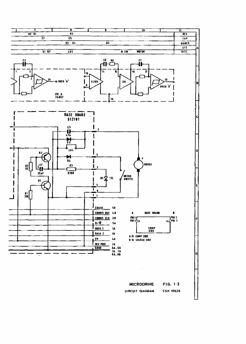
2. ZX MICRODRIVE (Figure 1.3)
2.1 The ZX microdrive is a ' f loppy tape' system used to store and retrieveup to 100 k bytes of information per cartridge. It is connected tothe Spectrum via ZX interface 1 and its own f l ex ib le ribbon cable, andhouses a l l its own read/write and motor control electronics wi th in itscase. Expansion port connectors on each microdrive al low up to 8devices to be plugged together and connected to one Spectrum computer.
1.5

2.2 The microdrive cartridge uses a continuous loop of 2 mm wide videotape. Data is written on two tracks using a standard stereo headarrangement and is writ ten in bytes, one byte to each track. Data isread from the tape in the same way. Software sees the tape as onecontinuous track since hardware takes care of switching betweentracks.
2.3 A l t h o u g h up to 8 microdrives can be connected together and controlledfrom 1 Spectrum, only 1 can be in use at any instant. The requiredmicrodrive and the type of operation, read or write, is selected undersoftware control . During a read operation data is read from theselected microdrive tape. During a write operation the microdrivetape is erased before being written. The erase head is displaced fromthe write head and is timed by IC1 to sink current before the writehead is enabled.
2.4 Microdrives are selected using the COMMS OUT and COMMS CLK signalsfrom IC1. Each microdrive control circuit (IC1 on the microdrivecircuit d iagram) , contains one stage of a shift register (a f l ip-flop) . COMMS CLK is connected to each microdrive and COMMS OUT isrouted via the expansion connector to the COMMS IN pin on the nextmicrodr ive , which is the input to the shift register. To select aparticular, micr-adrL^a a , ' 1 ' is shifted into its shift register to givei -i i on its Luiiiio uui pin.a i
2.5 COMMS OUT not only feeds the next microdrive; it is used to select itsown 1C internal functions and to select the LED, the motor, the erasecurrent and the write protect for the selected microdrive. Therefore,wh i l e this signal is low the motor is disabled, the LED is off , nocurrent can flow through the microdrive switch and therefore no erasecurrent can flow.
2.6 Consider the motor drive circuit. A high on pin 20 of Id turns onQl. This pulls the base of Q2 low turning it on and switching powerto the motor. Capacitor CIO and resistor R2 time constant ensure thatthe motor does not cut in too quickly and damage the tape. The redindicator LED D5 is switched on at the same time. With Q2 turned onand the write protect microswitch closed, the erase head currentcircuit is enabled via pin 6 of the headboard connector. When theerase output is enabled on pin 35 of Id, transistor Q9 switches onand current flows in the selected microdr ive erase head. Diodes D3and D4 provide protection against reverse currents. Diodes Dl , acrossthe erase head, and 02 perform similar functions. The amount ofcurrent f lowing in the erase head is l imited by IC1 and is about25 mA.
2.7 The write protect s igna l , WR PROT, on pin 32 of gate array IC1 isnormally low. A selected microdrive p u l l s this signal high when theWR PROT microswitch is closed. When the microdrive cartridge is notpresent or the write protect f lange is broken off this signal is low,informing the user that it cannot write.
1.6

2.8 Dur ing read/write operations the R / W signal on IC1 pin 23 places theselected microdr ive in either the read or the write mode, and enablesthe read or the write a m p l i f i e r s .
2.9 Data is recorded on 2 tracks us ing a standard stereo cassette headarrangement and is written in bytes, one byte to one track and thenext byte to the other track. It is recovered in the same way. Thetape itself is one continuous loop. Since hardware takes care ofswitching between tracks the software sees the tape as one double-length single t rack.
2.10 Power to the microdrive circuits has to be f i l tered and IC2 andcapacitors C3 and C4 are used to accomplish this.
2.11 Consider a read cycle. In the read mode the s ignals appearing in thetwo read coils inside the heads are d i f f e r e n t i a l l y ampl i f i ed throughtwo a m p l i f i e r chains w i t h i n IC1. The s ignals are then converted todigital form to enable logic processing. The outputs from the 2a m p l i f i e r s , in digital form are enabled into the DATA 1 and DATA 2outputs from IC1 on pins 24 and 19. These s ignals are routed to theinterface w i t h i n the gate array via microdrive edge connector J2.
2.12 The signal recorded on magnetic tape is at the greatest when the rateof change of the signal imposing it was at its fastest. Therefore,when a squarewave has been written, the greatest recovered vol tage isobtained on the edge of the pulse. Since the object is to produce awaveform which changes at the peaks of the recovered s i g n a l , IC1contains a m p l i f i e r s to br ing the signal up to the required l eve l , anda peak detect circuit which changes state when the input reaches itsgreatest level. The peak detector is followed by a hysteresis c i r cu i twhich ensures that the output does not change on spurious s igna l s .
2.13 The gain of the circuit should not need to be changed, as only onetype of high qua l i ty video tape is used. The reproduce s i gna l levelsmay be read across capacitors Cl and C2 and are typica l ly in the orderof 400 mV to 500 mV and 250 mV to 350 mV for the low frequency andhigh frequency signals respectively. In the record mode the modulatorin IC1 converts the ones and zeros in the data into FM (frequencymodula t ion ) where there is always a t ransi t ion at the b e g i n n i n g of thebit cell. If the data is a one there is a transition at the beginningand in the midd le of the bit c e l l , which means essentially that thefrequency doubles if the data contains ones.
2.14 The gain of the circuit can be adjusted if necessary by changing theratio of resistors R9 and R8 on p ins 15 and 14 of IC1.
2.15 Consider a write cycle. When the R/V signal from the gate array goeslow the selected microdrive is placed in the write mode. This has the
1.7

effect of changing DATA 1 and DATA 2 on IC1 from outputs to inputs.These inputs are used to drive current sources for track 1 and track2. When DATA 1 is h i g h , for example, current is pulled in onedirection through the head, when it is low current is p u l l e d inthe other direction. W r i t i n g is done with an asymmetric writecurrent. Because the erase function is carried out with a d.c. f ie ldit is necessary to write ' ha rde r ' in one direction than in the otherto overcome residual magnetism. Resistors R4 and R5 on pins 11 and 7of IC1 are chosen to allow this action. Should a different tape beintroduced or a different head type be fitted these resistors wouldalso need to be changed.
3. ZX INTERFACE 2
3.1 The ZX interface 2 connects directly to either the ZX interface 1module or to the Spectrum expansion connector. It provides theinterface for any joystick that has a standard 9-way D plug andenables the use of ZX ROM cartridge software. It also enablesjoysticks to be used with cassette-loaded programs and provides aconnector for a ZX printer.
3.2 The interface comprises 1 printed circuit board upon which are mounteda single integrated circuit and all the input/output connectors.
3.3 With the interface 2 connected to either the Spectrum or interface 1and with a ROM cartridge inserted, the ROMCS2 signal disables theSpectrum ROM and enables the Spectrum to interface with the ROMcartridge. The Spectrum CPU then uses its address, data and controlbusses to access the ROM via the expansion connector.
3.4 The interface 2 ULA is a custom-built CMOS integrated c i rcu i t whichplugs into the p.c.board mounted socket. Figure 1.4 gives a schematicof the device. Address bits AO. All and A12 are used to address the 2joysticks, with IORQ and "W performing their standard controlfunctions. Lines Kl to K9 receive the control inputs from the 2joysticks. The functions and connection details are summarised inthe table below.
PIN NO. SK3 SK4 FUNCTION
1 K9 K4 UP2 K8 K3 DOWN3 K6 Kl LEFT4 K7 K2 RIGHT56 KO K5 FIRE78 0V 0V COMMON9
NOTE: Kl to K9 correspond to keyboard keys 1 to 9
1.8

The rear edge connector provides connections for a ZX Printer.
4. POWER SUPPLY
The Spectrum power supply is capable of dr iv ing the Spectrum,interface 1, interface 2, ZX printer and 8 microdrives at the sametime.


SECTION 2
DISASSEMBLY/ASSEMBLY
Sub-Section LIST OF CONTENTS Page No.
1 Introduction 2.12 ZX Interface 1 2.13 ZX Microdrive 2.14 ZX Interface 2 2.2
1. INTRODUCTION
1.1 This section details the disassembly procedures for the two interfacesand the microdrive. In general the assembly procedure is the'reverse ofdisassembly although certain precautions are included where considerednecessary. The only tool reguired is a small cross-head screwdriver.
CAUTION
This eguipment contains CMOS integrated circuits.All surfaces and handling devices must be properlyearthed in order to avoid damage resulting fromelectrostatic discharge.
2. ZX INTERFACE 1
2.1 Turn the interface upside-down and remove 5 cross-head screws securingthe top cover to the base. Lift the base clear and place on one side.Remove two 5/8in self-tapping screws used to secure the interface to theSpectrum and turn the interface right-side up on a clean work surface.Remove the 2 cross-head screws securing the printed circuit board to thetop cover and while restraining the edge connector, ease the top coverclear.
2.2 Assembly is the reverse of disassembly remembering to replace the 5/8inself-tapping screws in the recesses provided BEFORE fitting and securingthe base.
3. ZX MICRODRIVE
3.1 Using a small blade screwdriver, c a r e f u l l y lift one corner of theadhesive cover trim. Having part ial ly separated the trim from the coverremove it completely and discard. Remove two cross-head screwsprevious ly obscured by the trim and after releasing a tongue positionedalong the back edge, separate the top cover from the base.
NOTE: The LED affixed to the cover is connected to the base p.c,boardvia f l y i n g leads. These prevent the cover and base beingseparated entirely.
2.1

3.2 To renew the motor assembly or components on either p.c.board it isadvisable to separate the base from the head chassis and base p.c.boardby preceeding as follows. Remove 2 cross-head screws securing the basep.c.board to the base and a further cross-head screw, accessible on theunderside of the microdrive, securing the base to the head chassis.
CAUTION
Having removed the base, take care not toplace excess strain on the flex cablesl i n k i n g the head and base p.c.boards.
Do not attempt to separate the head p.c.boards from the head chassis, as theread/write head a l ignment is cri t ical .Special tools are needed to re-align thisassembly.
3.3 Assembly is the reverse of disassembly taking care not to trap theflying leads between the head p.c.board and the base. After replacingthe top cover, fit a new adhesive trim.
4. ZX INTERFACE 2
4.1 Turn the interface upside-down and remove 4 cross-head screws. Afterlifting the base clear, the p.c.board is easily separated from the topcover.
4.2 Assembly is the reverse of disassembly taking care to orientate thep.c.board correctly.

SECTION 3
SYSTEM TEST
Sub-Section LIST OF CONTENTS Page No.
1 Introduction 3.12 ZX Interface 1 3.13 ZX Microdrive 3.24 ZX Interface 2 3.3
1. INTRODUCTION
1.1 The use of the fo l lowing test procedures is strongly recommended aftercarrying out unit repairs, thus ensur ing that a once defective unit iscompletely operational before return to the owner. The procedures mayalso be used effectively during fault diagnosis {Section 4) .
1.2 In each instance, where the list of test equipment specifies a ZXSpectrum, or ZX Interface 1 or a ZX Microdrive, use a workshopserviceable unit , NOT one returned by the customer.
2. ZX INTERFACE 1
2.1 The f o l l o w i n g are a number of tests to verify the operation of thevarious functions of the ZX Interface 1 unit. The Interface 1 shouldbe connected to a known good ZX Spectrum or Spectrum + and a knowngood ZX Microdrive.
(a) After switch-on, key in:
PRINT p [ENTER],
which should give the message 'Va r i ab l e not found1.
Then key in:
RUN [ENTER]
The message 'Program f in i shed ' should appear. This indicatesthat the paging mechanism is working, the ROM is funct ional , IC2and IC3 are funct ional , and that (at least) parts of the ULA andmost of the connections to the Spectrum are good. If the message'OK ' appears, this means that the ZX Interface 1 is not
functioning or not connected.
3.1

(b) Key in CAT 1 [ENTER].
If the red LED on the m i c r o d r i v e lights and the motor spinsbr ie f ly , this indicates that pins 29-32, 37 and 38 of the ULA arefunct ioning properly.
(c) To test the RS232 and NET ports, plug into the RS232 port a Dconnector with pins 2 and 3 shorted together, and p ins 4 and 5shorted together. Then run the f o l l o w i n g program:
The first part of the RS232 test checks the data send/receive,and the second part checks the DTK function. If the RS232function still does not work despite passing these two tests, theULA must be functioning and the voltage levels between the ULAand the RS232 socket should be checked.
(d) Clock Test: Try formatting a cartridge in the ZX Microdrive.If the screen border remains black during the first part of theformat, this indicates a clock problem in the Interface 1, andthe crystal circuit should be examined.
3. ZX MICRODRIVE
3.1 There are some basic tests that can be carried out using the fol lowingproyram. This should be run with the microdrive unit connected to aknown good system.

With a blank cartridge inserted in the Microdrive, the above programperforms a simple exercise of the 'write1, 'read' 'erase1functions.
3.2 An indication of another class of problem can be gained from thescreen dur ing the format operation. If the screen remains whiteduring the third stage of the format, this is a sign of noise on thewrite l ine . In this case, the motor alignment, the Microdrive ULA, orthe voltage regulator should be checked.
3.3 The waveforms at either end of Cl and C2 are significant for faultdiagnosis.
Key in:
OUT 239,252: OUT 239,254 [ENTER]
to set the ZX Microdrive spinning. Look at the waveform, ensuringthat the oscilloscope lead is earthed on the body of the regulator.There should be packets of o s c i l l a t i n g voltage (one long, two short),separated by quiet areas. The osci l la t ing voltage should be about0.5V peak-to-peak, but the important thing is that it should beconsistent, and not vary. The other important parameter is the noiselevel in the quiet patches. This should not be more than 25mV. Thebest way to check waveforms is to compare with those on a known goodunit.
4. ZX INTERFACE 2
4.1 The most practical test for the ZX interface 2 is a functional checkusing a suitable ROM cartridge (e.g. Space Raiders) and a pair ofindustry-standard joysticks.
3.3

4.2 ZX Interface 2 is plugged into the ZX Spectrum and the ROM cartridgesoftware RUN in the normal way. Provided the game employs joystickcontrols it is a simple matter to determine whether the game isrunning correctly and the UP, D O W N , L E F T , RIGHT and FIRE controlswitches are operational.
4.3 If the game does not run, suspect the ZX interface 2 p.c.board and/oredge connectors. The same applies if the joysticks are non-operat ional but also include a check of the 9-pin D-type connectorsand possible renewal of the ULA.

SECTION 4
FAULT DIAGNOSIS AND REPAIR
Sub-Section LIST OF CONTENTS Page Mo.
1 Introduction 4.12 Modif ica t ion History 4.23 Fault Diagnosis 4.4
Techniques 4.4In i t i a l Checks 4.4ZX Interface 1 4.5ZX Microdrive 4.6ZX Interface 2 4.8
4 Repair 4.8
1. INTRODUCTION
1.1 Section 4 is intended as a guide to the fault diagnosis and repair ofthe ZX interface 1, ZX microdr ive and ZX interface 2. It is assumedthat the service engineer has a reasonable knowledge of electronictheory, servicing and f a u l t - f i n d i n g techniques and has access to thetest equipment and tools required to carry out the task. Thefollowing items of test equipment and materials is the minimumrecommended:
(a) Oscilloscope with rise time 0.02 S/cm(b) Oscilloscope probe (X10)(c) Multimeter, general purpose(d) Head cleaner (Open market)(e) Motor location jig as shown:

1.2 For de ta i l s of how the ZX interfaces 1 and 2 and the ZX microdriveconnect to the Spectrum and for Spectrum operating procedures, referto the relevant m a n u a l s which accompany each uni t .
2 MODIFICATION HISTORY
2.1 ZX Interface 1. A s m a l l number of the EPROM vers ion of the ZXinterface 1 were produced. This version is characterised by a socket-mounted EPROM in the IC2 posi t ion and by IC3 and IC4 mounted pickabackfashion.
CAUTION
This version has no keyway on the microdriveedge connector. Take care when connecting akeyway-less ribbon connector, otherwise ashort-circuit could occur.
2.2 Where Q3, Q6 and Q9 are Ferranti type BC184P, these are inserted inthe opposite orientation to the pcb legend.
2.3 ZX Microdrive. A number of mod i f i ca t i ons have been introduced on themicrodrive. These m o d i f i c a t i o n s and the reasons for theirimplementat ion are summarised below:
(a) A 22uF capacitor C7 has been added across Q2 base to collector.This a l lows the motor to bu i ld up to running speed, rather thanchange from rest to speed immediately with the possibi l i ty ofdamage to tape. This modif icat ion should be checked for and ifnecessary fitted retrospectively.
(b) Capacitors Cl, C2, C6, and C8 have been changed from polystyreneto ceramic a x i a l , purely for convenience of production. Thev a l u e of Cl and C2 has also been changed from 150 pF to 22() pF.This value change should be checked for and if necessary fittedretrospectively.
(c) A 47nF capacitor has been added between pins 9 and 12 of IC1.This is a decoupl ing capacitor which prevents high frequencyinterference.
(d) The microswitch posi t ioning peg has been moved 1/2 mm towards thebase edge. In early issues, the microswitch moving arm can bebent by rough use, causing incorrect switch operation.
(e) The ratchet roller, ratchet and ratchet-spring (Fig 4.1) havebeen replaced by two rollers, one rubber and one plast ic , whichoperate more simply and economical ly . The ratchet is designed tostop a loop forming in the tape as the roller is turnedmechanically by the action of inserting the cartridge. In thedrive position the cartridge d i sab les the ratchet.


(f) A harder material has been used for the clamp spring. It hasbeen found that the o r i g i n a l material did not retain its springand sometimes reguired to be bent back to its original position.
(g) Where Ql is Ferranti type BC184P, this transistor is inserted inthe opposite orientation to the pcb legend.
2.4 ZX Interface 2. No problems have to date arisen with this uni t .
3. FAULT DIAGNOSIS
3.1 Techniques
3.1.1 In a closed loop system such as a computer, because of the inter-dependence of numerous component parts, fault d iagnosis is notnecessarily straight-forward. In add i t i on , because of the high speedcyclic operation, interpretation of any waveforms on control , data andaddress lines as being valid depends to a large extent on practicalexperience of the system.
3.1.2 Since the number of discrete components is limited it is possible thatthe major source of faults will be within integrated circuits.However before any 1C is chanyecl, waveforms and levels in the circuitmust be checked. Experience has shown that the best method ofi n i t i a l l y checking waveforms and levels can be to compare with thesame point in a known serviceable board. The fol lowing pages providea basic f a u l t - f i n d i n g procedure and a list of possible faults alongwith suggested remedies.
3.1.3 As a matter of course the suspect board should be inspected forobvious fau l t s such as burnt-out components or raised tracks. Edgeconnector pins should also be cleaned either with an eraser or anappropriate cleansing agent, applied with a small stencil brush andwiped clean with lint-free cloth. Pin connections should be inspectedfor damage.
3.1.4 Suspect units should be connected into the test system using workshopcables and connectors which are known to be serviceable. If asuccessful test result is obtained then the customer's cable/connectormust be faulty.
3.2 Initial Checks
3.2.1 Before power is applied to a suspect unit a check should be madebetween each power rail and 0V to isolate any short circuits. Checkfor open circuit between 0V and the pins set out in the fol lowingtable.
4.4

PIN 0V PINDEVICE CONNECTOR NO. (Ground) POWER RAIL
ZX Interface 1 SK4 3b 6b +5 V4b 6b +9 V
20a 6b -5 V22a 6b 412 V
ZX Microdrive Edge conn. 4b 6b +9 V
ZX Interface 2 Spectrum 3b 6b +5 Vedge conn. 4b 6b +9 V
3.3 ZX Interface 1
3.3.1 Wi th this uni t connected to a known serviceable system, apply power.Carry out the checks set out in the table below to establ ish startconditions.
CAUTION
Do not connect interface 1 with the power ONas damage to inductance LI and the ULA mayoccur.
FUNCTION C I R C U I T REE. WAVEFORM/VOLTAGE VALUE
On board d.c.powersupplies:
+5 V IC1 pin 40 5V d.c. ± 0.25 V -no discernable ripple.
-5 V Pin 20a of -5 V d.c.exp. conn.
+12 V Rll +12 V d.c.
-12 V R17 - 7 V d.c.
+ 9 V. R34 + 9 V d.c.
Clock pulses Id pin 5 8.0 MHz squarewave at+5 V amplitude
3.3.2 Carry out the ZX Interface 1 tests described in Section 3.2, whichalso gives details of fault diagnosis.

As an additional check, try loading a program from Microdrive. Thefo l lowing table l i s ts possible faults and remedies.
SYMPTOM REMEDY
Software does not load (1) Check for low on pin 20of IC2 and pin 6 of IC1.If high renew IC3.
(2) Renew IC2.(3) Renew ULA id.
Software does not run and Renew ULA IC1one of the f o l l o w i n g messagesdisplayed:
File not foundMicrodrive not present
3.4 ZX Microdrive
3.4.1 With the ZX microdr ive connected to a serviceable system, apply power.Establish that on-board voltages are correct by carrying out thechecks set out in the table below:
VOLTAGE C I R C U I T REF. VOLTAGE VALUE
+5 V IC1 P in : 11 +5 V7 +5 V9 +5 V,
no discernible ripple
+9 V Pin 10 of ribbon +9 Vconnector.
3.4.2 Perform the ZX Microdrive tests described in Section 3, para 3.1-3.2.The following table lists possible faults and remedies. For detaileddiagnosis, use the test in Section 3, para 3.3, as required.

SYMPTOM REMEDY
Messaye (1) Check and/or replace Q2.Microdrive not present (2) Renew IC1.
displayed
If program stops during:
Write test (1) Check R4, R5.(2) Renew IC1.
Read test (1) Check Cl, C2.(2) Renew IC1.(3) Renew w h o l e uni t .
Message Check microswitchWrite protect broken
displayed.
Microdrive does not operate (a) Check motor.although selected correctly (b) Check microdrive mechanics
for:
Tape being looped out of (i) Burrs on headspringscartridge causing jarmiing (check cartrid9e for
scratches).
Tight cartridge tape (n) Weak clamp spring(listen for clicks/-crunch sounds).
Broken tape (iii) Correct the operationof the ratchet/springassembly.
NOTE: If motor has over-heatedcheck for buckled base plate.Renew complete microdriveunit.
Head failure Renew complete microdrive unit.
LED failure Renew LED (LED is push-fitted).

3.5 ZX Interface 2
3.5.1 Since the ZX interface 2 comprises one integrated c i rcui t and a numberof connectors, fault f ind ing is simple. Connect the unit to aSpectrum and connect a games ROM cartridge, two joysticks and aprinter to the unit . Initiate the game and check out all functions.If a fault is found, power-down and replace IC1. Printer faults mustbe due to d iscont inui ty between input and output, since pin to pinconnections are used.
4. REPAIR
4.1 Renewal of components should be carried out using recogniseddesoldering/heatsinking techniques to prevent damage to the componentor the printed circuit board. General points to note are:
(a) The head assembly in the microdrive is the only component whichMUST NOT be changed.
(b) When replacing the plug-in 1C in interface 2 use the correctremoval and insertion tools.
(c) When handling ICs take normal anti-static precautions. It isrecommended that only a suitably earthed, low power solderingiron be used.
(d) When removing a soldered-in 1C, cut each pin and remove thecomponent before individually unsoldering each pin.
(e) After any component has been removed the p.c. board should beexamined carefully to ensure that there are no solder 'splatters'which may cause short circuits between tracks or connector pins.
(f) Disassembly/assembly instructions are given in Section 2.
4.2 Actions to take to rectify problems encountered in the mechanicaloperation of the microdrive are set out in the following paragraphs.
Replace the motor as follows:
(a) Insert the motor and loosely assemble the fixing screws.
(b) Insert the motor location jig to position the motor.
(c) Tighten fixing screws.
NOTES: 1. When renewing the motor also renew the plastic and therubber drive rollers. If the motor has a combined rubberroller and ratchet, discard complete ratchet assembly andreplace with the rubber and plastic roller.

2. The gap between the rubber roller and the plastic rollershould be 0.25 millimetre.
(d) Perform the following motor drive test:
(i) With a cartridge inserted and the motor running, push thecartridge gently away from the motor drive roller untiltape movement ceases.
(ii) Release the cartridge. It should return under the actionof the clamp spring and tape movement restart without anyrattling or noise. If this is not the case, thenprovided that the clamp spring is set satisfactorily, thehead spring must be adjusted as follows. (Never adjustnew type clamp spring which has a loop below chassislevel).
(e) If the motor drive test above indicates that the head springneeds adjusting, this is done as follows:
(i) Unscrew the motor and push the head spring downwards oneach side of the head to achieve the dimension shownbelow.
(ii) Replace the motor and set its position with the motorlocation jig.
4.3 The two problems associated with faulty mechanical operation of thecartridge are burrs on the head springs and a weak clamp spring.Both faults prevent the cartridge from being firmly pushed into thedrive position and can cause intermittent operation, tape-spill etc.
4.4 Burrs on the head springs may be filed off using a small flatinstrument file. Take care not to damage the drive roller on themotor side.
4.5 The clamp spring may be bent back into position using a pair ofbull-nosed pliers. The final position of the spring should bewithin the diameter of the adjacent head-assembly post.

SECTION 5
PARTS LIST
Sub-Section LIST OF CONTENTS Page No.
1 In t roduct ion 5.1ZX Interface 1 Table 5.1 PCB Assembly 5.1
Table 5.2 Case Assembly 5.4ZX Microdrive Table 5.3 Head Board Assembly 5.4
Table 5.4 Base Board Assembly 5.5Table 5.5 Head Chassis Assembly 5.5Table 5.6 Case Assembly 5.6
ZX Interface 2 Table 5.7 Assembly 5.6
1. INTRODUCTION
1.1 The f o l l o w i n g parts t ab le s list only those components consideredpracticable to renew. The mic rod r ive record/playback is not l istednei ther are the side, head and ratchet springs.
TABLE 5.1 ZX INTERFACE 1 PCB ASSEMBLY
Circuit Value Rat ing Manufacturer / NotesReference Tolerance Type
CAPACITORS
C1.C2 47yF 16V Electrolyt ic AxialC3 lOOpF 5%, 50V Ceramic AxialC4 22 pF 5%,50V Ceramic AxialC5 47 nF +80%,-20%,50V - Axia lC6 47UF 16V Electrolytic AxialC7.C8 330pF 10%, 50V 'Tayo1 sx±a±
COIL
LI 22MH 0.41 A
DIODES
D1,D2 BA157 Rec t i f i e rD3.D4 1N4148 SignalD6 to D8 4.3V 500 mV BZX79C4V3 ZenerD9 to Dll 1N4148 Signal
(continued)
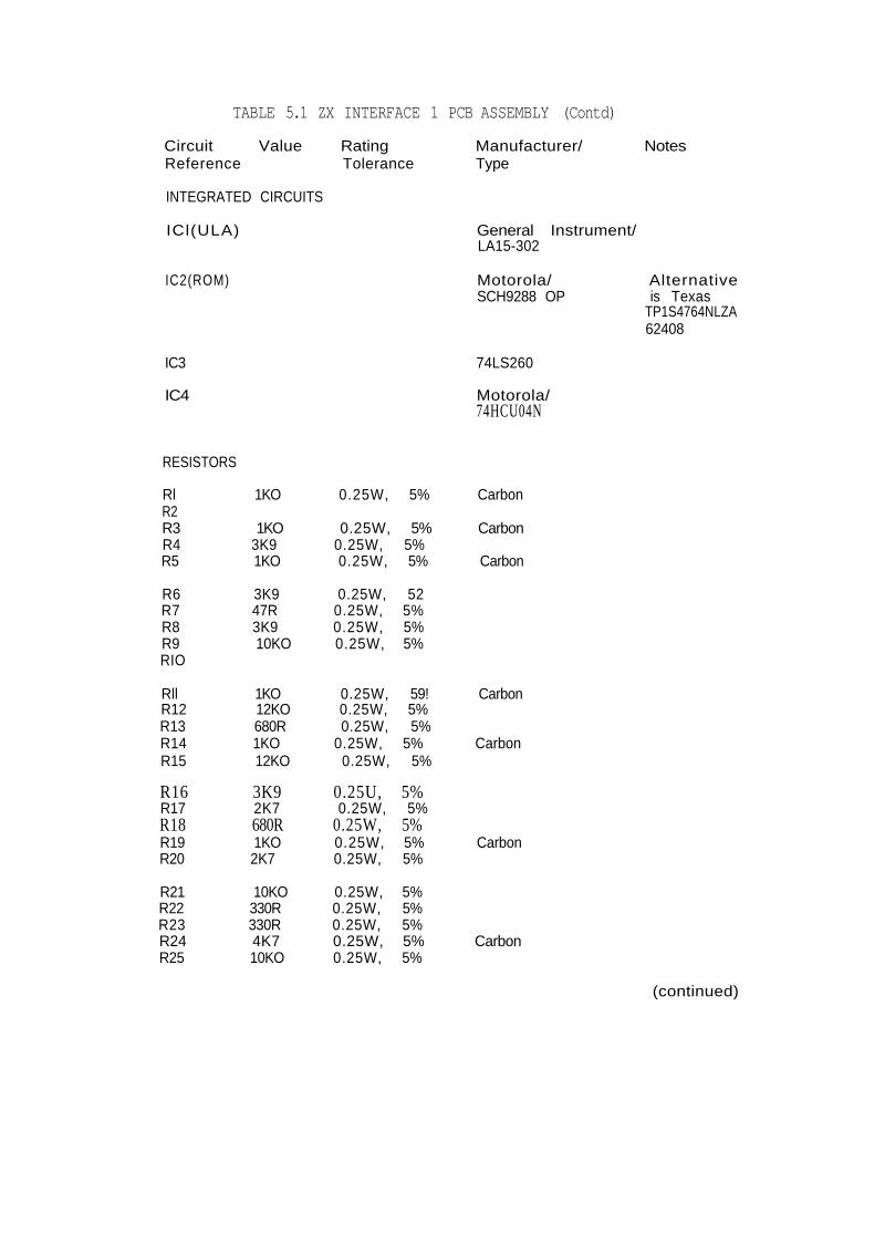
TABLE 5.1 ZX INTERFACE 1 PCB ASSEMBLY (Contd)
Circuit Value Rating Manufacturer/ NotesReference Tolerance Type
INTEGRATED CIRCUITS
ICl(ULA) General Instrument/LA15-302
IC2(ROM) Motorola/ AlternativeSCH9288 OP is Texas
TP1S4764NLZA62408
IC3 74LS260
IC4 Motorola/74HCU04N
RESISTORS
Rl 1KO 0.25W, 5% CarbonR2R3 1KO 0.25W, 5% CarbonR4 3K9 0.25W, 5%R5 1KO 0.25W, 5% Carbon
R6 3K9 0.25W, 52R7 47R 0.25W, 5%R8 3K9 0.25W, 5%R9 10KO 0.25W, 5%RIO
Rll 1KO 0.25W, 59! CarbonR12 12KO 0.25W, 5%R13 680R 0.25W, 5%R14 1KO 0.25W, 5% CarbonR15 12KO 0.25W, 5%
R16 3K9 0.25U, 5%R17 2K7 0.25W, 5%R18 680R 0.25W, 5%R19 1KO 0.25W, 5% CarbonR20 2K7 0.25W, 5%
R21 10KO 0.25W, 5%R22 330R 0.25W, 5%R23 330R 0.25W, 5%R24 4K7 0.25W, 5% CarbonR25 10KO 0.25W, 5%
(continued)
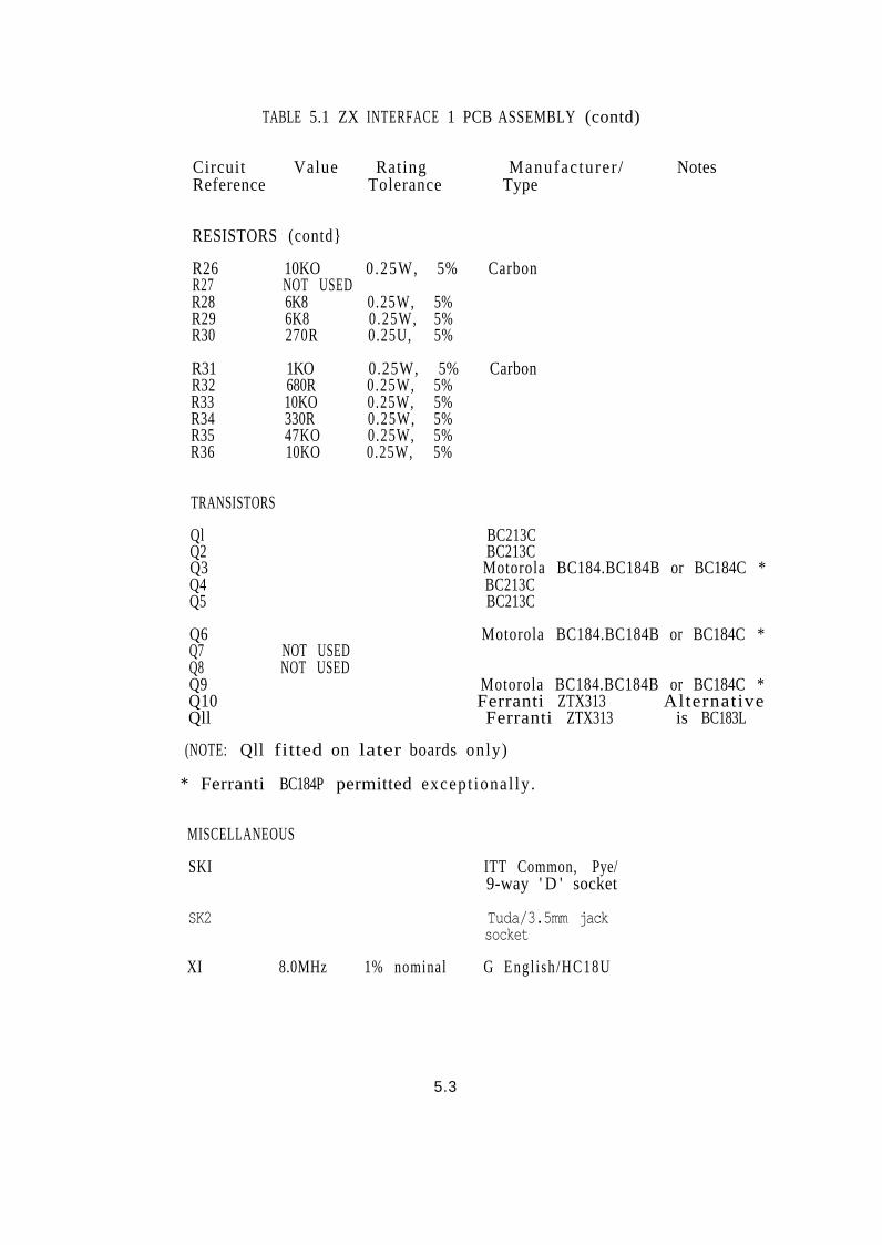
TABLE 5.1 ZX INTERFACE 1 PCB ASSEMBLY (contd)
Circuit Value Rating Manufac turer / NotesReference Tolerance Type
RESISTORS (contd}
R26 10KO 0 .25W, 5% CarbonR27 NOT USEDR28 6K8 0.25W, 5%R29 6K8 0 .25W, 5%R30 270R 0.25U, 5%
R31 1KO 0.25W, 5% CarbonR32 680R 0 .25W, 5%R33 10KO 0.25W, 5%R34 330R 0.25W, 5%R35 47KO 0.25W, 5%R36 10KO 0.25W, 5%
TRANSISTORS
Ql BC213CQ2 BC213CQ3 Motorola BC184.BC184B or BC184C *Q4 BC213CQ5 BC213C
Q6 Motorola BC184.BC184B or BC184C *Q7 NOT USEDQ8 NOT USEDQ9 Motorola BC184.BC184B or BC184C *Q10 Ferranti ZTX313 AlternativeQll Ferranti ZTX313 is BC183L
(NOTE: Qll fitted on later boards only)
* Ferranti BC184P permitted except ional ly .
MISCELLANEOUS
SKI ITT Common, Pye/9-way ' D ' socket
SK2 Tuda/3.5mm jacksocket
XI 8.0MHz 1% nominal G Eng l i sh /HC18U
5.3

TABLE 5.2 ZX INTERFACE 1 CASE ASSEMBLY
Item Description Manufacturer/Type
Cover - Kenure/512110Base - Kenure/512111Screw (2 off) C'sk, 4.2 mm x 5/8 in Ig PlastiteScrew (2 off) C'sk, 4.2 mm x 3/8 in Ig PlastiteScrew {5 off) C'sk, 4.2 mm x 1/2 in Ig PlastiteRibbon Cable Interface 1 to Microdrive VarelcoJack Cable 3.5 mm jack ends x 2 m Ig Able
TABLE 5.3 ZX MICRODRIVE HEAD BOARD ASSEMBLY
Circuit Value Rating Manufacturer/ NotesReference Tolerance Type
RESISTORS
R4 150 0.25W, 5% CarbonR5 180 0.25W, 5* CarbonR6 to R9 4K7 0.25W, 5% Carbon
CAPACITORS
Cl 220 pF 2.5% Ceramic Axia lC2 220 pF 2.5% Ceramic Axia lC3 0.47pF 50 V Electrolytic AxialC4 0.22uF 50V Electrolytic Axia lC6 330 pF 2.5% Ceramic Axial
C7 NOT USEDC8 330pF 2.5% Ceramic AxialC9 NOT USEDCIO 48nF +80%,-20%, 50V Tayo Axial
DIODES
Dl - - 1N4148 SignalD2 1N4148 Signal
INTEGRATED CIRCUITS
IC1 (ULA) Ferranti/ULA2G007
IC2 5V 78M05 Regulator

TABLE 5.4 ZX MICRODRIVE BASE BOARD ASSEMBLY
Circuit Value Rating Manufacturer/ NotesReference Tolerance Type
RESISTORS
Rl 33KO 0.25W, 5% CarbonR2 1KO 0.25W, 5% CarbonR3 820 Q.25W, 554 CarbonRIO - - - Link
CAPACITORS
C5 47nF +80%, -20%, 50V - AxialC7 22UF - Electrolytic Axial
DIODES
D3 - - IN4148 SignalD4 1N4148 Signal
TRANSISTORS
Ql * - - Motorola BC184,BC184B or BC184C
Q2 - - Ferranti ZTX551
* Ferranti BC184P permitted except ional ly .
TABLE 5.5 ZX MICRODRIVE HEAD CHASSIS ASSEMBLY
Item Description Manufacturer/Type
Head Assembly. This component must not be changed.
Motor 9V, 2400 rpm, Mabuchi EG-500AD-9Fclockwise rotation
Drive Rol ler Smooth wa l l RE componentsPlastic R o l l e r
Microswitch - Burgess
Screw (2 off) C ' s k , 4 mm.Pos idr ive M2.5
Screw (1 off) Pan hd, 2.28 mm x Plastite3/8 1g

TABLE 5.6 ZX MICRODRIVE CASE ASSEMBLY
Item Description Manufacturer/Type
Cover - Kenure S12090
Base - Kenure S12095
Cover Trim Spectrum Logo James Cook S12095
LED Red G Engl i s h / L N 2 8 P P ( T )
Inner Flex 5 way x 1 in flex cable Dean
Outer Flex 5 way x 1 1/2 in f l ex cable Dean
Connector 7 way daisy-chain Pye S12102
Screw (4 of f ) Pan hd,4 .2 mm x 1/4 in Ig Plasti te
Screw (1 off) Pan hd ,4 .2 mm x 1/2 in Ig Plastite
Screw (2 off) C ' s k . 4 . 2 mm x 3/8 in Ig Plastite
TABLE 5.7 ZX INTERFACE 2
Item Description Manufacturer/Type
IC1 ( U L A ) Integrated Circuit MCE HT62001
SKI 28-way edge connector Pye
SK2 15-way edge connector Pye
SK3.SK4 9-way ' D ' type connector ITT Cannon
Upper case - Can ton -Hi l l SRC126
Lower case - Canton-Hill SRC127
Case lid - Canton-Hi l l SRC128
Screw (4 off) C ' s k , 2 . 9 mm x 13 mm Ig Plastite

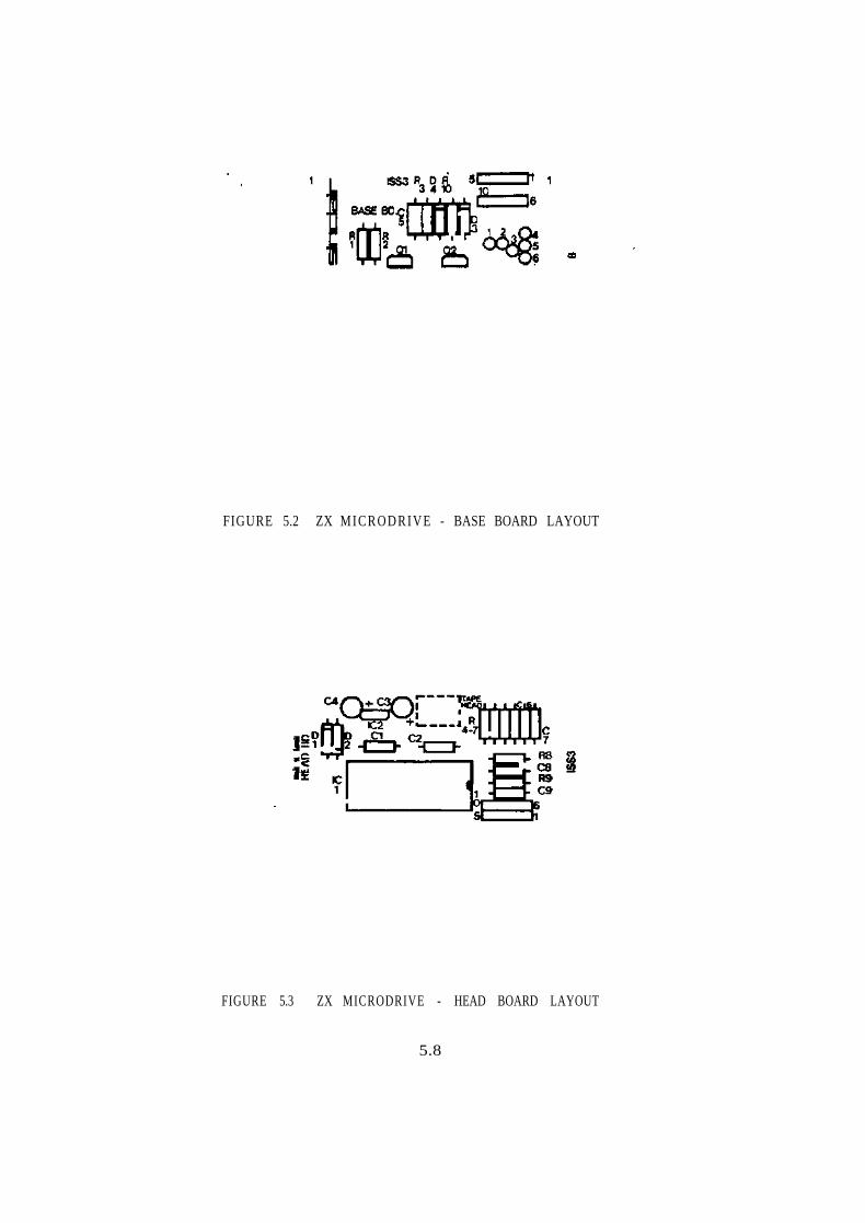
FIGURE 5.2 ZX M I C R O D R I V E - BASE BOARD LAYOUT
FIGURE 5.3 ZX MICRODRIVE - HEAD BOARD LAYOUT
5.8


![[ZX] Changement d'un joint de culasse sur une ZX 1xud9te.free.fr/Download/Tutorial/[ZX]Changement_joint... · 2008. 11. 30. · [ZX] Changement d'un joint de culasse sur une ZX 1.9D](https://img.dokumen.tips/doc/110x75/60d4a95281e5cb60cf64541b/zx-changement-dun-joint-de-culasse-sur-une-zx-zxchangementjoint-2008.jpg)