Embed Size (px)
Citation preview

XAPP1111 (v1.0 ) April 13, 2009 www.xilinx.com 1
© 2009 Xilinx, Inc. All rights reserved. XILINX, the Xilinx logo, and other designated brands included herein are trademarks of Xilinx, Inc. All other trademarks are the property of their respective owners.
Abstract This application note demonstrates how to run a simulation of an EDK system containing the PLBv46 Endpoint Bridge for PCI Express® core. The simulation consists of a PCIe® Downstream Port Model communicating over a PCIe bus to an EDK system containing the PLBv46 Endpoint Bridge for PCI Express. The Downstream Port Model is build using the Xilinx Core Generator tool. The PLBv46 Endpoint Bridge uses the Xilinx Block Plus Endpoint core for PCI Express in the Virtex®-5 FPGA. C code running on the PowerPC 440 drives the EDK system.
Xilinx provides a simulation environment based on a Downstream Port Model (DPM) which has a Test Program Interface (TPI) for test programs. Pre written programs and Verilog tasks are used to generate Transaction Layer Packets (TLPs). The setup of the simulation and steps used to run the system simulation are provided as part of this application note. Example stimuli for root complex to endpoint and endpoint to root complex transactions test the PLBv46 Endpoint Bridge in the EDK system. The results from the tests are analyzed in the waveform viewer.
Included System
The project for the system simulation is available at:
https://secure.xilinx.com/webreg/clickthrough.do?cid=119479
In xapp1111.zip, the project directory is ml507_ppc440_plbv46_pcie_sim, and the sub-directory simulation contains most of the files used in this application note.
Introduction The PLBv46 Endpoint Bridge is a PCIe endpoint instantiated in a Xilinx FPGA. An endpoint normally communicates with a root complex or switch. In this system simulation, the PLBv46 Endpoint Bridge in the EDK system is connected to a test environment based on a Downstream Port Model, which emulates the functionality of a root complex for test purposes. This application note shows how to run a system simulation of an EDK system which uses the PLBv46 Endpoint Bridge.The EDK system is based on a Base System Builder creation of a system using the Xilinx ML507 Embedded Development Platform.
After describing the system, the steps to setup and run a simulation are provided. The first step is to ensure that the EDK, ISE, and Smartmodel libraries are compiled and referenced by the EDK system properly. Within an EDK project, the structure and contents of the simulation directory is discussed. The commands used to generate the EDK simulation model and the Downstream Port Model model are discussed. The script used to run the simulation is discussed.
In the simulation, stimuli is generated from both the Downstream Port Model side and the PLBv46 side. The stimuli for the Downstream Port Model is provided in the rc2ep.v file. The C code stimuli is provided in the pcie_dma.c file. The Xilinx PCIe simulation environment uses a Downstream Port Model which connects to test programs using at Test Program Interface (TPI). Xilinx provides ten programs which use the TPI. The test programs use Verilog tasks to setup the simulation, configure and scan the Configuration Space Header, and generate memory and completion TLPs. The steps to use the Xilinx PCIe simulation environment and to write and use custom tests are provided.
Application Note: Embedded Processing
XAPP1111 (v1.0) April 13, 2009
Simulation of an EDK System Which Uses the PLBv46 Endpoint Bridge for PCI ExpressAuthor: Lester Sanders
R

Software Requirements
XAPP1111 (v1.0 ) April 13, 2009 www.xilinx.com 2
R
Software Requirements
The software requirements for simulating this system are:
• Xilinx Platform Studio 10.1.03
• Xilinx Integrated Software Environment (ISE®) 10.1.03
• ModelSim 6.3c (Both VHDL and Verilog are required)
System Specifics
The PCIe Downstream Port Model (DPM) and the EDK system are used in this simulation. The Downstream Port Model is a set of Verilog files written using Coregen when the Xilinx LogiCORE PCIe core is generated. Since these files are provided in the simulation/dsport directory, running Coregen is not necessary for this simulation. Since the EDK system is developed using EDK’s Base System Builder, the Processor IP cores are listed in the system.mhs file.
Figure 1 shows a functional diagram of the system simulated.
Figure 2 is the block diagram of the EDK system. The EDK system includes the PPC440MC DDR2 Controller, XPS BRAM, XPS INTC, Clock Generator, XPS UART Lite, XPS Central DMA, and PLBv46 Endpoint Bridge cores. An EDK simulation in which the PLBv46 is driven by Bus Functional Models instead of C code is given in XAPP1110. In both cases, the user is able to write and read registers and memory of the processor IP cores in the EDK system.
X-Ref Target - Figure 1
Figure 1: System Simulation
X-Ref Target - Figure 2
Figure 2: EDK System
X1111_01_111008
DownstreamPort
EDKSystem
rc2ep.v
TxP RxP
TxN RxN
RxN TxN
RxP TxP
DDR2
PowerPC 440
XPSINTC
PLBv46PCIe
XPSUART Lite
ClockGenerator
XPSBRAM
X1111_02_111008
PPC440MCDDR2
XPS CentralDMA
XPS GPIO
PLB_v46_1
PLB_v46_0

System Specifics
XAPP1111 (v1.0 ) April 13, 2009 www.xilinx.com 3
R
Table 1 provides the address map of the system.
In EDK, double click on the PCIe_Bridge in the System Assembly View to invoke the PLBv46 _PCIe generics editor. The generics are used to configure the PLBv46 Endpoint Bridge. The Xilinx Device ID = 0x0505 and Vendor ID = 0x10EE are displayed in many of the PCIe tests done in this application note.
Table 1: EDK System Address Map
Peripheral Instance Base Address High Address
XPS INTC xps_intc_0 0x81800000 0x8180FFFF
Clock Generator clock_generator_0 N/A N/A
XPS BRAM CNTLR xps_bram_if_cntlr_1 0xFFFF0000 0xFFFFFFFF
XPS Central DMA xps_central_dma_0 0x80200000 0x8020FFFF
PLBv46 Endpoint Bridge PCIe_Bridge 0x85C00000 0x85C0FFFF
XPS Uartlite RS232_Uart_1 0x84000000 0x8400FFFF
PPC440 Memory Controller DDR2_SDRAM 0x00000000 0x0FFFFFFF
XPS GPIO LEDs_8Bit 0x81400000 0x8140FFFF

Compiling Simulation Libraries
XAPP1111 (v1.0 ) April 13, 2009 www.xilinx.com 4
R
Compiling Simulation Libraries
This section illustrates how to compile EDK, ISE, and Smartmodel simulation libraries.
Figure 3 shows the first step in compiling simulation libraries. Invoke EDK, and enter File -> Open to open an EDK project. Select Simulation -> Compile Simulation Libraries.
X-Ref Target - Figure 3
Figure 3: Selecting Compiling Simulation Libraries
X1111_03_111008

Compiling Simulation Libraries
XAPP1111 (v1.0 ) April 13, 2009 www.xilinx.com 5
R
Figure 4 shows the use of the Simulation Library Compilation wizard in compiling simulation libraries. Click Next.
X-Ref Target - Figure 4
Figure 4: Using the EDK Simulation Library Compilation Wizard
X1111_04_111008

Compiling Simulation Libraries
XAPP1111 (v1.0 ) April 13, 2009 www.xilinx.com 6
R
Figure 5 shows the selection of ModelSim v6.3c in compiling simulation libraries. The wizard displays the version of the ModelSim simulator that was detected. If this is grayed out, then the simulator is not set up properly. Click Next.
X-Ref Target - Figure 5
Figure 5: Selecting the ModelSim Simulator
X1111_05_111008

Compiling Simulation Libraries
XAPP1111 (v1.0 ) April 13, 2009 www.xilinx.com 7
R
Figure 6 shows the selection of both the VHDL and Verilog. Click Next.
X-Ref Target - Figure 6
Figure 6: Selecting both Verilog and VHDL for Mixed Simulation
X1111_06_111008

Compiling Simulation Libraries
XAPP1111 (v1.0 ) April 13, 2009 www.xilinx.com 8
R
Figure 7 shows the specification of the directory for ISE library and Smartmodels. Click Next.
X-Ref Target - Figure 7
Figure 7: Defining the Install Directories of ISE_Lib, Smartmodels
X1111_07_111008

Compiling Simulation Libraries
XAPP1111 (v1.0 ) April 13, 2009 www.xilinx.com 9
R
Figure 8 shows the specification of the directory for the EDK libraries. Click Next.
Set Environment Variables shown below as appropriate for the simulation environment.
XILINX=/build/aqxfndry2/K.39.0/rtf; export XILINX
XILINX_EDK=/proj/abq_ip/edk_builds/EDK_K_SP3.6.1/rtf; export XILINX_EDK
MTI_LIBS=/scratch/simlib/EDK10.1.03_mti_se_linux; export MTI_LIBS
LMC_HOME=$MTI_LIBS/smartmodel; export LMC_HOME
LMC_CONFIG=$LMC_HOME/data/x86_linux.lib; export LMC_CONFIG
LMC_PATH=$LMC_HOME/foundry:$LMC_HOME/models; export LMC_PATH
LM_LIBRARY_PATH=$LMC_HOME/lib/linux.lib:LM_LIBRARY_PATH; export LM_LIBRARY_PATH
If the Windows operation system is used, include %LMC_HOME%\lib\pcnt.lib in the Path under System variables.
If the Linux operating system is used, set the following lines in the modelsim.ini file.
veriuser = $LMC_HOME/lib/linux.lib/swiftpli_mti.so
libsm = $MODEL_TECH/libsm.sl
X-Ref Target - Figure 8
Figure 8: Defining the Install Directory of EDK_Lib
X1111_08_111008
Simulation Directory Structure
XAPP1111 (v1.0 ) April 13, 2009 www.xilinx.com 10
R
libswift = $LMC_HOME/lib/linux.lib/libswift.so
If the Windows operating system is used, set the following lines in modelsim.ini.
veriuser = %LMC_HOME%/lib/pcnt.lib/swiftpli_mti.dll
libsm = %MODEL_TECH%/libsm.dll
libswift = %LMC_HOME%/lib/pcnt.lib/libswift.dll
Set the simulation resolution to ps. Use a semicolon to comment the line
PathSeparator = /
To verify that the SmartModels are set up correctly, enter the following in the ModelSim command window:
VSIM> vsim unisim.ppc405
If there are no errors when loading, the SmartModels are set up correctly.
Simulation Directory Structure
The xapp1111.zip project directory, ml507_ppc440_plbv46_pcie_sim, contains the simulation directory at the top level of the ml507_ppc440_plbv46_pcie_sim project. The simulation directory contains the scripts, ddr2 dsport, and testbench sub-directories. When simgen is run, the behavioral sub-directory is created under the simulation directory.
Figure 9 shows the directory structure of the simulation environment.
The behavioral directory contains the wrappers which use core models in EDK_Lib to provide a model of the EDK system.
The dsport directory contains the verilog files which model the Downstream Port. The files are
• board.v
• dsp_cfg.v - Downstream Port configuration file
• pcie_exp_1_lane_64b_dsport.v - Downstream Port Simulation Model
• pci_exp_usrapp_cfg.v
• pci_exp_usrapp_com.v - Downstream Port Configuration Interface Controller
• pci_exp_usrapp_rx.v - Endpoint to Downstream Port Model tasks
• pci_exp_usrapp_tx.v - Downstream Port Model to Endpoint tasks
X-Ref Target - Figure 9
Figure 9: Simulation Directory Structure
scripts testbenchdsport
simulation
X1111_09_121008
ddr2behavioral

Simulation Directory Structure
XAPP1111 (v1.0 ) April 13, 2009 www.xilinx.com 11
R
• xilinx_pci_exp_defines.v - Various parameter definitions
• xilinx_pci_exp_downstream_port.v - top level Downstream Port Model file
• xilinx_pci_exp_dsport.v - Instantiates Downstream Port
The testbench directory contains the testbench.v file. The testbench.v file instantiates the Downstream Port Model and the EDK system, which is the device under test (DUT). The testbench.v also defines the clocks and resets for both downstream and EDK systems. The tests.v file contains the names of the test program which drives the Downstream Port Model. It may contain rc2ep.v or a user-developed test program.
The project’s simulation/ddr2/256Mb_ddr2 directory contains the ddr2.v file for simulations which use the Linux operating system, and the ddr2.v_nt for systems which use the Windows operating system. To simulate using Windows, copy ddr2.v_nt to ddr2.v.
The scripts directory contains the files and commands used to compile the Downstream Port Model and testbench.
The run.do file compiles the pcie_x1.f file. The pcie_x1.f file is the list of files used in the Downstream Port Model. The run.do runs the simulation for the time specified in the last line of the run.do file.

Generating Simulation Models with Simgen
XAPP1111 (v1.0 ) April 13, 2009 www.xilinx.com 12
R
Generating Simulation Models with Simgen
Before running simgen, edit the simgen.opt -X argument to specify the location of the ISE Lib compiled in the section “Compiling Simulation Libraries”, and the -E argument to specify the location of the EDK_Lib.
Simgen can be run from EDK or a command prompt. Figure 10 shows how to run simgen from EDK. Select Simulation -> Generate Simulation HDL Files.
X-Ref Target - Figure 10
Figure 10: Running Generate Simulation HDL Files from EDK
X1111_10_111008

Running a Simulation
XAPP1111 (v1.0 ) April 13, 2009 www.xilinx.com 13
R
To run simgen from the command line, create simgen.opt as shown in Figure 11.
Run
simgen -f simgen.opt
If running simgen from the EDK GUI, modify library path values using
Edit -> Preferences -> Application Preferences -> Simulation Libraries Path
Running a Simulation
Do the following steps to run a simulation. From the project’s root directory
cd simulation/behavioral
Invoke ModelSim using the command
vsim &
X-Ref Target - Figure 11
Figure 11: simgen.opt
system.mhs -pxc5vlx50tff1136-2-langverilog-peppc_440_0pcie_dma/executable.elf-mixedyes-smti-X/scratch/simlib/EDK10.1.03_mti_se_linux/ISE_Lib-E/scratch/simlib/EDK10.1.03_mti_se_linux/EDK_Lib-mbeh
X1111_11_121008

Running a Simulation
XAPP1111 (v1.0 ) April 13, 2009 www.xilinx.com 14
R
In ModelSim, select View -> Workspace. As shown in Figure 12, verify that the EDK and ISE libraries are correct and available. If the correct libraries are not displayed, copy the /scratch/simlib/EDK10.1_03_mti_se_linux/EDK_Lib/modelsim.ini to the project’s simulation/behavioral directory and verify that the libraries are correct.
X-Ref Target - Figure 12
Figure 12: Verifying Libraries Using View -> Workspace
X1111_12_111008

Running a Simulation
XAPP1111 (v1.0 ) April 13, 2009 www.xilinx.com 15
R
Figure 13 shows the compilation of the EDK system. Run
do system.do
in the transcript window.
X-Ref Target - Figure 13
Figure 13: Compiling the EDK System
X1111_13_111008

Running a Simulation
XAPP1111 (v1.0 ) April 13, 2009 www.xilinx.com 16
R
Figure 14 shows the expected results from compiling the EDK system. The Processor IP wrappers in the behavioral directory and the system.v file are compiled.
In the ModelSim transcript window run
do ../scripts/run.do
If there is a compilation error, verify that the -L XilinxCoreLib_ver argument is included in the vsim command in run.do If the compilation error persists and the NT operating system is used, add the -novopt argument to the vsim command.
X-Ref Target - Figure 14
Figure 14: Compiled EDK System
X1111_14_111008

Running a Simulation
XAPP1111 (v1.0 ) April 13, 2009 www.xilinx.com 17
R
Figure 15 shows the transcript window which displays the PLL lock and link training of the PCIe cores in the Downstream Port Model and the PLBv46 Endpoint Bridge. The resets are done at 5 us. FE is an abbreviation for Far End, referring to the Downstream Port Model. Link training starts at 26 us and is complete at 80 us.
If the simulation transcript window does not indicate that the PCIe link is trained, and the Downstream Port Model does not generate active signals on TxP, TxN, verify that the Smartmodels are set up correctly. While the Endpoint for PCI Express core and the GTPs in the Virtex-5 FPGA use SecureIP models, the GT11 transceiver models in the Downstream Port use Smartmodels in ISE 10.1.03.
X-Ref Target - Figure 15
Figure 15: Simulation Startup
X1111_15_111008

Running a Simulation
XAPP1111 (v1.0 ) April 13, 2009 www.xilinx.com 18
R
Figure 16 shows that the memory controller calibrated at 71135 ns.
X-Ref Target - Figure 16
Figure 16: Memory Controller Calibration
X1111_16_111008

Running a Simulation
XAPP1111 (v1.0 ) April 13, 2009 www.xilinx.com 19
R
Figure 17 shows the simulation startup in the ModelSim waveform viewer. The trn_reset_n signal is inactive at 5 us.The PCIe_Bridge (DUT) generates Training Sequence (TS) packets at 23 us. The Downstream Port Model generates TS packets at 57 us. The trn_lnk_up_n is active at 80 us.
The waveform viewer contains dividers for the PCIe Bridge, BRAM, DDR2, and Central DMA signals. In the waveform figures in this application note, only a limited number of signals are displayed. Additional signals need to be viewed to understand most simulations. This requires running the simulation and to scrolling through signals for each active IP in the waveform viewer.
X-Ref Target - Figure 17
Figure 17: Waveform of Simulation Startup
X1111_17_111108

Stimuli from the PCIe side
XAPP1111 (v1.0 ) April 13, 2009 www.xilinx.com 20
R
Stimuli from the PCIe side
In this application note, Downstream Port Model to endpoint transactions are done using the testbench/rc2ep.v file.
The Xilinx simulation environment for PCI Express includes the Downstream Port Model tests listed in Table 2. These tests are provided in two files, sample_smoke_tests.v and pio_tests.v, in the simulation/testbench directory. These tests are listed for reference and are not discussed in this application note.
Xilinx provides 40 Verilog tasks for use in the test program which connects to the Downstream Port Model through the TPI. The Verilog source for many of the tasks is given in the simulation/dsport/pci_exp_usrapp_tx.v file. The tasks accept input and write to and read from the DPM PCIe core’s Local Link interface. Table B-4 in UG341 provides the inputs/arguments for the 40 pre-written Verilog tasks.
The rc2ep.v file calls the Type 0 Configuration Read and Configuration Write Verilog tasks and Memory Read and Memory Write tasks. The four Verilog tasks used in rc2ep.v are listed in Table 3.
Table 2: Downstream Port Model Tests
Test Name Description
sample_smoke_test0Issues a PCI Type 0 Configuration Read TLP, waits for Completion TLP, and compares the value with the Device/Vendor ID expected value.
sample_smoke_test1 Same as sample_smoke_test0 but uses parallel tests as defined in UG341
pio_writeReadBack Transmits a 1 DWORD Write TLP followed by a 1 DWORD Read TLP, waits for Completion TLP, and verifies results.
pio_testByteEnables_test0 Issues four sequential Write TLPs enabling a unique byte enable, and then a Read TLP to verify the results
pio_memTestDataBus Runs a walking 1s address test on BRAM
pio_memTestAddrBus runs a walking 1s address test on BRAM
pio_memTestDevice Runs an increment/decrement test on BRAM
pio_timeoutFailureExpected Sends a MWr32TLP followed by a MRd32 TLP to an invalid address and waits for a CplD TLP
pio_tlp_test0 Example which issues a sequence of Read and Write TLPs to the RX interface
Table 3: Commonly Used Verilog Tasks
Tasks Arguments
TSK_TX_TYPE0_CONFIGURATION_READ tag, address, first_dw_be
TSK_TX_TYPE0_CONFIGURATION_WRITE tag, address, data, first_dw_be

Stimuli from the PCIe side
XAPP1111 (v1.0 ) April 13, 2009 www.xilinx.com 21
R
PCIe to PLBv46 stimuli is provided in rc2ep.v. To provide an overview of rc2ep.v, most of rc2ep.v is shown in Figure 18. The rc2ep.v file begins with the TSK_SIMULATION_TIMEOUT and TSK_SYSTEM_INITIALIZATION tasks.
The rc2ep.v file then reads the Configuration Space Header (CSH) of the PLBv46 Endpoint Bridge using the TSK_TX_TYPE0_CONFIGURATION_READ task. In Figure 19, the Device ID/Vendor ID is read. In the actual rc2ep.v, the Command/Status, Class code/Revision ID and Header/Latency/Cache registers are also read. For reading and writing the Endpoint Configuration Space Header (CSH), the argument is the offset address of the register that is read or written.
This is followed by a configuration write of the Command/Status register, located at offset address x04, and then the Base Address Register 0 (BAR0), located at offset address x10 in the CSH. The TSK_TX_TYPE0_CONFIGURATION_WRITE task is used. The second argument provides the CSH offset, and the third argument provides the data written.
The PCI BAR0 is actually a 64 bit BAR, and is written by two configuration writes to CSH offsets x10 and x14. Offset x10 is the least significant word and offset x14 is the most significant word, so the PCIBAR0 starting address is 0x0000000060000000.
With BAR0 defined, memory writes are done to 0x60000000 using the TSK_TX_MEMORY_WRITE_32 task. To verify that the memory write is correct, this is followed by a memory read using the TSK_TX_MEMORY_READ_32 task.
Unlike TSK_TX_TYPE0_CONFIGURATION_WRITE, there is no data argument in the TSK_TX_TYPE_MEMORY_WRITE_32 task. The data written in the memory write task, TSK_TX_MEMORY_WRITE_32, is written into the DATA_STORE structure in rc2ep.v.
The TSK_TX_COMPLETION_DATA task sends a CplD TLP in response to a Memory Read TLP sent by the PLBv46 Endpoint Bridge in the EDK system.
TSK_TX_MEMORY_WRITE_32 tag, tc, length, address, last_dw_be, first_dw_be
TSK_TX_MEMORY_READ_32 tag, tc, length, address, last_dw_be, first_dw_be
Table 3: Commonly Used Verilog Tasks
Tasks Arguments

Stimuli from the PCIe side
XAPP1111 (v1.0 ) April 13, 2009 www.xilinx.com 22
R
The rc2ep.v file can be edited to perform a variety of tests. In the remainder of this section, single and burst PCIe to PLBv46 transactions are done. Besides standard configuration writes/reads and memory writes/reads, rc2ep.v can be edited to cause the Endpoint Bridge in the EDK system to transmit TLPs which cause interrupts to be generated. These are referred to as abnormal transactions in the Xilinx PLBv46 Endpoint Bridge documentation. Several examples are given in “Abnormal PCIe to PLBv46 Transactions”.
In most applications, the functionality of IP cores in the EDK system is controlled by either the PowerPC or MicroBlaze processor. As an alternative, rc2ep.v can control the functionality of IP cores in the EDK system over the PCIe link. An example is given in “Controlling EDK Functions from the PCIe Side”.
Note: The rc2ep.v and the testbench.v files provided in xapp1111.zip cannot do all of the tests provided in this application note. The files may or may not be edited for each specific test. This application note provides excerpts of the tasks which need to be run for each test.
Understanding transactions in the Downstream Port Model
The DPM is a simulation model which acts as a pseudo Root Complex interface to the PLBv46 Endpoint Bridge. The DPM is not a complete system. It does not have memory. The principal interfaces in the DPM are the transmit local link interface trn_td and receive local link interface trn_rd. This section provides training needed to understand PCIe transactions in the DPM. The
X-Ref Target - Figure 18
Figure 18: Display of the rc2ep.v file
TSK_SIMULATION_TIMEOUT(5050);
TSK_SYSTEM_INITIALIZATION;
$display(”[%t] : - Device/Vendor ID = 0x%08x”, $realtime, P_READ_DATA);TSK_TX_TYPE0_CONFIGURATION_READ(DEFAULT_TAG, 12’h000, 4’hf );
$display(”[%t] : - Command/Status Register = 0x%08x”, $realtime);TSK_TX_TYPE0_CONFIGURATION_WRITE(DEFAULT_TAG, 12’h004, 32’hFFFFFFFF, 4’Hf );
$display(”[%t] : - BAR = 0x%08x”, $realtime);TSK_TX_TYPE0_CONFIGURATION_WRITE(DEFAULT_TAG, 12’h10, 32’h60000000, 4’hf );TSK_TX_TYPE0_CONFIGURATION_WRITE(DEFAULT_TAG, 12’h14, 32’h00000000, 4’hf );
$display(”[%t] : RC to EP Single Tests”, $realtime);
DATA_STORE[0] = 8’h78;DATA_STORE[1] = 8’h56;DATA_STORE[2] = 8’h34;DATA_STORE[3] = 8’h12;
TSK_TX_MEMORY_WRITE_32(DEFAULT_TAG, DEFAULT_TC, 10’d1, ‘h60000000, 4’h0, 4’hF, 1’b0)
TSK_TX_MEMORY_READ_32(DEFAULT_TAG, DEFAULT_TC, 10’d1, ‘h60000000, 4’h0, 4’hF)
TSK_WAIT_FOR_READ_DATA;
#20000TSK_TX_COMPLETION_DATA(DEFAULT_TAG, DEFAULT_TC, 10’d1, 12’d4, 7’b0000000, 3’h0, 1’b0)
X1111_18_121008

Stimuli from the PCIe side
XAPP1111 (v1.0 ) April 13, 2009 www.xilinx.com 23
R
Xilinx Live e-Learning course Designing a LogiCore PCI Express System provides examples and a lab on using the PCIe local link interface.
Figure 19 shows a configuration read from the rc2ep.v file. The Xilinx Device ID/Vendor ID is provided at the local link trn_rd signal at 78480 ns. The following line in rc2ep.v is the stimuli for reading the PLBv46 Endpoint Bridge CSH.
TSK_TX_TYPE0_CONFIGURATION_READ(DEFAULT_TAG, 12’h000, 4’hF);
In the waveform, the trn_rd link contains the CplD TLP. The 4A defines the TLP as a CplD packet. The returned data, ee100505, indicates that the Device ID of the Endpoint is x0505, and the Vendor ID is x10EE. The next pages provide a description of how to read TLPs in the DPM.
X-Ref Target - Figure 19
Figure 19: Configuration Read from the Downstream Port Model
X1111_19_121008

Stimuli from the PCIe side
XAPP1111 (v1.0 ) April 13, 2009 www.xilinx.com 24
R
Figure 20 shows the transcript window indicating the time of the configuration transactions in the DPM. The TSK_PARSE_FRAME task in the dsport/pci_exp_usrapp_com.v displays in the transcript window the time a TLP is generated or received in the DPM.
After noting the TSK_PARSE_FRAME output in the transcript window, there are two ways of understanding the TLPs transmitted and received in the DPM. The tx.dat and rx.dat log files in the simulation/behavioral directory provide information on DPM transactions. The second method, illustrated briefly in Figure 19, is to analyze the trn_td and trn_rd signals in the ModelSim waveform viewer. The next figures show excerpts from the log files and show how to identify common TLP transactions transmitted and received by the DPM.
X-Ref Target - Figure 20
Figure 20: Transcript of Configuration Reads
X1111_20_121008

Stimuli from the PCIe side
XAPP1111 (v1.0 ) April 13, 2009 www.xilinx.com 25
R
The Downstream Port Model uses a Local Link interface. Table 4 provides format information for reading data on the trn_rd and trn_td local link interfaces. The last column in this table provides the type of transaction transmitted or received by the Downstream Port Model. As an example, the trn_rd signals in Figure 19 have a value of 0x4A000001 when trn_rsof_n becomes active. From Table 4, the 4A indicates that a Completion with Data (CPLD) TLP is received.
Table 5 lists the Format field. This shows the 32 and 64 bit TLPs in the previous table for MRd and MWr TLPs.
Table 4: Downstream Port Model Local Link Commands
Type Format (1:0) Type(4:0) Description trn_td[63:56], trn_rd[63:56]
MRd0001
0 0000 Memory Read Request 00
MWr1011
0 0000 Memory Write Request 40
CfgRd0 00 0 0100 Type 0 Configuration Read 04
CfgWr0 01 0 0100 Type 0 Configuration Write 44
Cpl 00 0 1010 Completion without Data 0A
CplD 10 0 1010 Completion with Data 4A
Table 5: Format Field
FMT[10] TLP Format
00 3 DW Header, No Data
01 4 DW Header, No Data
10 3 DW Header, With Data
11 4 DW Header, With Data

Stimuli from the PCIe side
XAPP1111 (v1.0 ) April 13, 2009 www.xilinx.com 26
R
Figure 21 shows an excerpt from the DPM transmit log file, tx.dat, after running a simulation with rc2ep.v. The transmit TLPs are the write tasks defined in testbench/rc2ep.v. The tx.dat file shows a configuration read of the Device/Vendor ID and the Command/Status registers in the Configuration Space Header, at 77402 and 83898 ns. To get the result of the two reads, open rx.dat and look for CplD TLPs sometime following the Memory Read request times in tx.dat.
X-Ref Target - Figure 21
Figure 21: Downstream Port Model tx.dat file
X1111_21_121008

Stimuli from the PCIe side
XAPP1111 (v1.0 ) April 13, 2009 www.xilinx.com 27
R
Figure 22 shows excerpts of the rx.dat file for the DPM. The rx.dat log file is the result of DPM read tasks in rc2ep.v and/or read or write commands across the PCIe link from PLBv46 Endpoint Bridge in the EDK system, which is driven by the ep2rc.bfl. file. The TLPs in the figure are the result of memory write and memory read commands in ep2rc.bfl.
X-Ref Target - Figure 22
Figure 22: Downstream Port Model rx.dat File
X1111_22_121008

Stimuli from the PCIe side
XAPP1111 (v1.0 ) April 13, 2009 www.xilinx.com 28
R
Figure 23 shows the Configuration Write TLP on the DPM trn_td local link. The task in rc2ep.v is:
TSK_TX_TYPE0_CONFIGURATION_WRITE(DEFAULT_TAG, 12’h04, 32’hFFFFFFFF, 4’hF)
In this task, the 12’h04 offset is the Command Status Register in the Configuration Space Header. The third argument is the data written. All Fs are written to the Command/Status register to avoid looking up each bit.
The trn_td signal shows 44 as the type Configuration Write as defined in Table 4, followed by the 0xFFFFFFFF payload.
X-Ref Target - Figure 23
Figure 23: Downstream Port Model Configuration Write TLP
X1111_23_121008

Stimuli from the PCIe side
XAPP1111 (v1.0 ) April 13, 2009 www.xilinx.com 29
R
Figure 24 shows DPM memory write TLP on trn_td. The task in rc2ep.v is:
TSK_TX_MEMORY_WRITE_32(DEFAULT_TAG, DEFAULT_TC, 10’d1, 32’h60000000, 4’h0, 4’hF, 1’b0)
Setting the third argument, the length field, to 10’d1, causes a single DWORD write to be generated. A burst transaction is generated when the length field is > 1. The forth argument, the address, is 32’h60000000. Since the 32‘h60000000 address is the same address written in the configuration write statements in rc2ep.v to define BAR0 (offset x10, x14), this TLP will be recognized by the PLBv46 Endpoint Bridge.
X-Ref Target - Figure 24
Figure 24: Memory Write TLP
X1111_24_121008

Stimuli from the PCIe side
XAPP1111 (v1.0 ) April 13, 2009 www.xilinx.com 30
R
Figure 25 shows the Downstream Port Model Memory Read TLP on trn_td. The task in rc2ep.v which generates the read is:
TSK_TX_MEMORY_READ_32(DEFAULT_TAG, DEFAULT_TC, 10’d1, 32’h60000000, 4’h0, 4’hF)
Setting the third argument, the length field, to 10’d1, causes a single DWORD read to be generated. A burst transaction is generated when the length field is > 1. The address is 32’h60000000, the address written in the configuration read statements in rc2ep.v.
The memory read operation begins with a transmission of a type 00 Memory Read TLP on trn_td. After a relatively long cycle, a (type 4A) CplD TLP is received on trn_rd.
Abnormal PCIe to PLBv46 Transactions
The next figures show how to generate abnormal conditions. Abnormal conditions are not desirable. The motivation for learning about abnormal conditions is to facilitate quick debug of incorrect behavior.
The Master Completion Abort (MCA) is asserted when the master side of the Endpoint Bridge receives an Abort from the PLB. To cause a MCA interrupt, change the C_PCIBAR2IPIFBAR_0 generic in system.mhs from 0x90000000, the address of DDR2, to 0x60000000, an address without a target. Re-run the simgen command.
The Global Interrupt Enable and Bridge Interrupt Enable registers are written in ep2rc.bfl. The rc2ep.v write command does not change:
X-Ref Target - Figure 25
Figure 25: Downstream Port Model Memory Read TLP
X1111_25_121008

Stimuli from the PCIe side
XAPP1111 (v1.0 ) April 13, 2009 www.xilinx.com 31
R
TSK_TX_MEMORY_WRITE_32(DEFAULT_TAG, DEFAULT_TC, 10’d1, 32’h60000000, 4’h0, 4’hF, 1’b0)
Figure 26 shows the Master Completer Abort interrupt.
X-Ref Target - Figure 26
Figure 26: Master Completer Abort Interrupt
X1111_26_121008

Stimuli from the PCIe side
XAPP1111 (v1.0 ) April 13, 2009 www.xilinx.com 32
R
To generate a Non-Contiguous Byte Enable interrupt, the original system.mhs is used. The sixth argument in the memory write task in the rc2ep.v file, First Byte Enable, is changed from 0xF to 0xA.
TSK_TX_MEMORY_WRITE_32(DEFAULT_TAG, DEFAULT_TC, 10’d1, 32’h60000000, 4’h0, 4’hA, 1’b0)
Figure 27 shows the interrupt due to non-contiguous byte enables.
X-Ref Target - Figure 27
Figure 27: Interrupt Due to Non-contiguous Byte Enable(s)
X1111_27_121008

Stimuli from the PCIe side
XAPP1111 (v1.0 ) April 13, 2009 www.xilinx.com 33
R
The interrupt due to a poisoned payload is generated by changing the last field in the memory write task in the rc2ep.v file from 0 to 1.
TSK_TX_MEMORY_WRITE_32(DEFAULT_TAG, DEFAULT_TC, 10’d1, 32’h60000000, 4’h0, 4’hF, 1’b1)
Figure 28 shows the interrupt due to a Poison bit.
Controlling EDK Functions from the PCIe Side
The rc2ep.v file can be edited so the DPM controls operations within the EDK system from the PCIe side. Typical applications include controlling the SPI or IIC cores in the EDK system.
Another application is to control the DMA Controller in the EDK system from the PCIe side. This may address the performance issue of PCIe to PLBv46 read operations. Write transactions are faster than read transactions. To transfer data from the EDK system memory to the DPM, a DMA operation controlled by the DPM may increase throughput.
X-Ref Target - Figure 28
Figure 28: Poison Bit Interrupt
X1111_28_121008

Stimuli from the PCIe side
XAPP1111 (v1.0 ) April 13, 2009 www.xilinx.com 34
R
To initiate a DMA operation, the rc2ep.v file controls the XPS Central DMA Controller in the EDK System. The use of the DMA Controller is defined in the section “Stimuli from the PLBv46 side”. To control the DMA controller with the DPM, set C_PCIBAR2IPIFBAR = x80200000, the base address of the XPS DMA Controller in the system.mhs file, and re-run simgen.
The rc2ep.v code below shows the control of the DMA controller from PCIe side. Four memory write tasks write to the control, source address, destination address, and length registers in the DMA controller. The data written to these registers is stored in the DATA_STORE array. The data is set for each write task.
-- Write DMA Controller Control Register
DATA_STORE[0] = 8’hC0;DATA_STORE[1] = 8’h00;DATA_STORE[2] = 8’h00;DATA_STORE[3] = 8’h04;
TSK_TX_MEMORY_WRITE_32(DEFAULT_TAG, DEFAULT_TC, 10’d1, 32’h80200004, 4’h0, 4’hF, 1’b1)
-- Write DMA Controller Source Address
DATA_STORE[0] = 8’h90;DATA_STORE[1] = 8’h00;DATA_STORE[2] = 8’h00;DATA_STORE[3] = 8’h00;
TSK_TX_MEMORY_WRITE_32(DEFAULT_TAG, DEFAULT_TC, 10’d1, 32’h80200008, 4’h0, 4’hF, 1’b1)
-- Write DMA Controller Destination Address
DATA_STORE[0] = 8’hA0;DATA_STORE[1] = 8’h00;DATA_STORE[2] = 8’h00;DATA_STORE[3] = 8’h00;
TSK_TX_MEMORY_WRITE_32(DEFAULT_TAG, DEFAULT_TC, 10’d1, 32’h8020000C, 4’h0, 4’hF, 1’b1)
-- Write DMA Controller Length
DATA_STORE[0] = 8’h00;DATA_STORE[1] = 8’h00;DATA_STORE[2] = 8’h10;DATA_STORE[3] = 8’h00;
TSK_TX_MEMORY_WRITE_32(DEFAULT_TAG, DEFAULT_TC, 10’d1, 32’h80200010, 4’h0, 4’hF, 1’b1)

Stimuli from the PLBv46 side
XAPP1111 (v1.0 ) April 13, 2009 www.xilinx.com 35
R
The tasks in the rc2ep.v file cause the DMA Controller in the EDK system to transfer data from XPS BRAM across the PCIe link. This transaction involves operations from the DPM, BRAM, PLBv46 Endpoint Bridge, and XPS Central DMA Controller, so analysis requires running a simulation and scrolling through the waveform viewer signals.
Figure 29 shows the XPS Central DMA in the EDK system reading BRAM at address 0x8AE10000 and writing the data to the C_IPIFBAR0 address 0xA0000000. This address is translated across the PCIe link to the DPM.
Stimuli from the PLBv46 side
In this simulation, C code is used to write and read EDK peripherals, both registers and memory. The software project for the simulation, pcie_dma, contains the pcie_dma.c file.
To generate transactions, pcie_dma.c writes either directly to the PLBv46 Endpoint Bridge C_IPIFBAR0 address or to the XPS Central DMA Controller source/destination address which is a C_IPIFBAR0 address.
Table 6 shows the locations of the registers in the XPS Central DMA used for DMA operations. A DMA operation is initiated by writing to these four registers.
X-Ref Target - Figure 29
Figure 29: DMA Controller Controlled from PCIe Side
X1111_29_121008

Stimuli from the PLBv46 side
XAPP1111 (v1.0 ) April 13, 2009 www.xilinx.com 36
R
Figure 30 shows the flow chart for pcie_dma.c. The source region data is written with barberpole data. The destination memory is written as zeroes. The DMA operation is done by writing to the four XPS Central DMA registers listed in Table 6. In the supplied version of pcie_dma.c, verification is not done.
Table 6: XPS Central DMA Registers
DMA Register Address
Control Register C_BASEADDR + 0x04
Source Address Register C_BASEADDR + 0x08
Destination Address Register C_BASEADDR + 0x0C
Length Register C_BASEADDR + 0x10
X-Ref Target - Figure 30
Figure 30: Flow Chart for pcie_dma.c
X1111_30_121008
ZeroRegion
DMARegion
BarberpoleRegion
Verify

Stimuli from the PLBv46 side
XAPP1111 (v1.0 ) April 13, 2009 www.xilinx.com 37
R
Figure 31 shows the parameters in pcie_dme.c which are the source address and destination address for the DMA operations.As shown in Table 6, these addresses are located at XPS Central DMA C_BASEADDR offsets of 0x8 and 0xC.
X-Ref Target - Figure 31
Figure 31: DMA Controller Source and Destination Address in pcie_dma.c
#define MEM_0_BASEADDR 0xFFFF0000#define MEM_1_BASEADDR 0xC0000000
DMALength = 1024
X1111_31_121008
Stimuli from the PLBv46 side
XAPP1111 (v1.0 ) April 13, 2009 www.xilinx.com 38
R
Figure 32 shows the waveform of the write and read of the Bridge Control Register of the PLBv46 Endpoint Bridge. This shows a value of 0x85C001e0 on PLB_ABus when PLB_PAvalid is high and a value of 0x003F0107 on PLB_Wrdbus when sl_wrcomp is active.
X-Ref Target - Figure 32
Figure 32: Writing the Bridge Control Register
X1111_32_121008

Stimuli from the PLBv46 side
XAPP1111 (v1.0 ) April 13, 2009 www.xilinx.com 39
R
Figure 33 shows a waveform in which the XPS Central DMA Controller Control register located at 0x80200004 is written with 0xC000004.
X-Ref Target - Figure 33
Figure 33: Writing the XPS Central DMA Controller Control Register
X1111_33_121008

Stimuli from the PLBv46 side
XAPP1111 (v1.0 ) April 13, 2009 www.xilinx.com 40
R
Figure 34 shows a waveform in which the XPS Central DMA Controller’s Source Address register is written with the base address of XPS BRAM.
X-Ref Target - Figure 34
Figure 34: Writing DMAC Controller Source Address
X1111_34_121008
Stimuli from the PLBv46 side
XAPP1111 (v1.0 ) April 13, 2009 www.xilinx.com 41
R
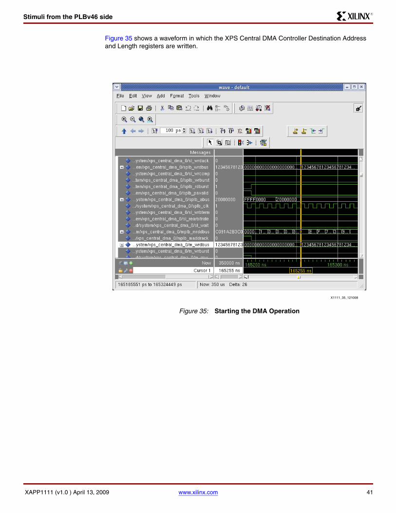
Figure 35 shows a waveform in which the XPS Central DMA Controller Destination Address and Length registers are written.
X-Ref Target - Figure 35
Figure 35: Starting the DMA Operation
X1111_35_121008

Stimuli from the PLBv46 side
XAPP1111 (v1.0 ) April 13, 2009 www.xilinx.com 42
R
Figure 36 shows DMA Controller operation at the DPM. Burst data is received on trn_rd.
X-Ref Target - Figure 36
Figure 36: DMA Operations
X1111_36_121008

References
XAPP1111 (v1.0 ) April 13, 2009 www.xilinx.com 43
R
References 1. UG197 Virtex-5 Integrated Endpoint Block for PCI Express Designs User Guide
2. UG341 LogiCORE Endpoint Block Plus v1.7 for PCI Express User Guide - April 25, 2008
3. XAPP1030 Reference System: PLBv46 PCIe in the ML505 Embedded Development Platform
4. XAPP1110 BFL Simulation of an EDK System which Uses the PLBv46 Endpoint Bridge for PCI Express
5. XAPP1000 Reference System: PLBv46 PCIe in the ML555 PCI/PCIE
Revision History
The following table shows the revision history for this document.
Notice of Disclaimer
Xilinx is disclosing this Application Note to you “AS-IS” with no warranty of any kind. This Application Note is one possible implementation of this feature, application, or standard, and is subject to change without further notice from Xilinx. You are responsible for obtaining any rights you may require in connection with your use or implementation of this Application Note. XILINX MAKES NO REPRESENTATIONS OR WARRANTIES, WHETHER EXPRESS OR IMPLIED, STATUTORY OR OTHERWISE, INCLUDING, WITHOUT LIMITATION, IMPLIED WARRANTIES OF MERCHANTABILITY, NONINFRINGEMENT, OR FITNESS FOR A PARTICULAR PURPOSE. IN NO EVENT WILL XILINX BE LIABLE FOR ANY LOSS OF DATA, LOST PROFITS, OR FOR ANY SPECIAL, INCIDENTAL, CONSEQUENTIAL, OR INDIRECT DAMAGES ARISING FROM YOUR USE OF THIS APPLICATION NOTE.
Date Version Revision
4/13/09 1.0 Initial release.