Embed Size (px)
Citation preview

Xilinx Solution Guide Spring 2013
1
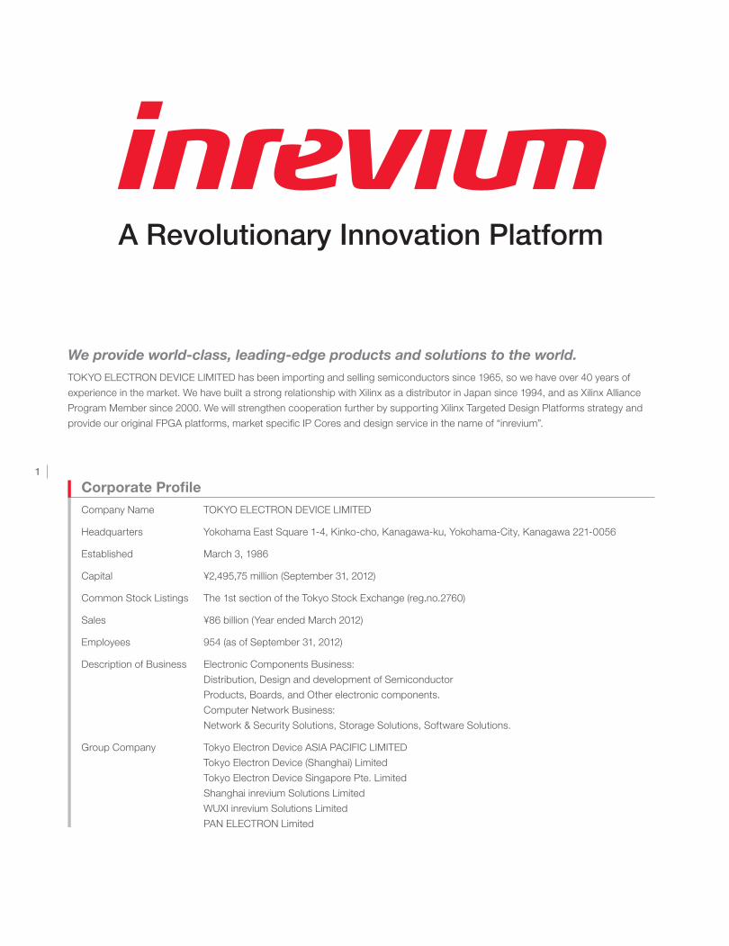
Corporate ProfileCompany Name TOKYO ELECTRON DEVICE LIMITED
Headquarters Yokohama East Square 1-4, Kinko-cho, Kanagawa-ku, Yokohama-City, Kanagawa 221-0056
Established March 3, 1986
Capital ¥2,495,75 million (September 31, 2012)
Common Stock Listings The 1st section of the Tokyo Stock Exchange (reg.no.2760)
Sales ¥86 billion (Year ended March 2012)
Employees 954 (as of September 31, 2012)
Description of Business Electronic Components Business:
Distribution, Design and development of Semiconductor
Products, Boards, and Other electronic components.
Computer Network Business:
Network & Security Solutions, Storage Solutions, Software Solutions.
Group Company Tokyo Electron Device ASIA PACIFIC LIMITED
Tokyo Electron Device (Shanghai) Limited
Tokyo Electron Device Singapore Pte. Limited
Shanghai inrevium Solutions Limited
WUXI inrevium Solutions Limited
PAN ELECTRON Limited
We provide world-class, leading-edge products and solutions to the world.TOKYO ELECTRON DEVICE LIMITED has been importing and selling semiconductors since 1965, so we have over 40 years of
experience in the market. We have built a strong relationship with Xilinx as a distributor in Japan since 1994, and as Xilinx Alliance
Program Member since 2000. We will strengthen cooperation further by supporting Xilinx Targeted Design Platforms strategy and
provide our original FPGA platforms, market specific IP Cores and design service in the name of “inrevium”.
A Revolutionary Innovation Platform

2
inrevium Solution Sales Offices & Design Centers
TOKYOELECTRONDEVICEWorld Headquarters– Sales Of�ce– Design Center
TOKYOELECTRONDEVICEShanghai– Sales Of�ce– Design Center
TOKYOELECTRONDEVICESINGAPORE PTE. LTD.– Sales Of�ce
TOKYOELECTRONDEVICEKOREA OFFICE– Sales Of�ce
TOKYOELECTRONDEVICEUS Of�ce (CA)– Sales Of�ce
Focus your time and domain expertise on Differentiation
Communication – Video – AVBMarket speci�c IP, custom tools, custom boards
Embedded – DSP – ConnectivityDomain IP, Domain tools, FMC daughter cards
Virtex – SpartanBase IP, ISE program, base boards
Application
Market-Speci�c
Domain-Speci�c
Base Platform
ALLIANCE PROGRAMPREMIER MEMBER
Premier Certified Member
Lead member for Targeted Design Platforms 3
IP optimization for Xilinx (Required) 3
Early Xilinx technology adopter 3
Enhanced factory support 3
Extensive on-site audit 3
Company certification 3 3
Certified engineers 3 3
Early access to technology roadmap 3 3 3
Qualified via application process 3 3 3
Member Levels
Xilinx Targeted Design Platform
Xilinx Alliance Program Premier MemberTokyo Electron Device is a Premier Member of the Xilinx Alliance Program and delivers the
highest level of market- and domain-specific expertise and pre-qualified solutions through
Xilinx Targeted Design Platforms. As a Premier Member, TED has gone through a stringent
certification process to ensure that its products and services are optimized to streamline
customer product development cycles while minimizing risk.
TED supports the Xilinx Targeted Design Platforms strategy and provides original base
boards, FMC daughter cards, market-specific, IPs and kits.

3
Design ServiceOpened in 1985, the Design & Development Center uses
its wealth of customer project experience and the latest
equipment to provide specialized customer design services.
The Development Center also creates market specific multi-
million gate LSI devices, FPGA evaluation boards, ASIC
prototyping boards, drivers, firmware and IP to support
a wide range of leading edge applications in the audio,
consumer video, broadcast video connectivity, high-speed
communication, computer peripheral, medical and industrial
automation markets.
Original IP CoreTED develops IP cores for Xilinx FPGAs compliant with
new-generation interfaces based on customer needs.
inrevium Solution
Design Service
inrevium PlatformLeading Edge Xilinx
Customer Needs
IP Core

Original Design Manufacturer (ODM)From the initial stages of determining specifications
through to actual manufacture of mass-produced
products and implementation of quality control measures,
TED provides its customers with a one-stop source
to meet their needs. TED aids in the selection, design
and development of components scheduled for mass
production and strives to optimize costs.
TED is also able to work in collaboration with partner
manufacturers in the leading areas of specific fields in
order to flexibly respond to customers’ ever-diversifying
range of requirements.
PartnershipTED works closely with a number of high-level partners to
provide the best FPGA platforms in the market.
inrevium PlatformLeading Edge Xilinx
Customer Needs
ODM Board
Partnership
4

5
Virtex®-7 FPGA ASIC Development Test PlatformPart Number : TB-7V-2000T-LSI
Reference Design (Verilog HDL)EHigh-speed DDR3 SDRAM Interface Design
– Memory controller : 1066Mbps, 32bit data width, Generated by Memory Interface Generator (MIG)
EUSB 2.0/3.0 Interfaces Design
FeaturesEFPGA
– XC7V2000T-2FLG1925 device– XC7K325T-2FFG900 device
EMemory – DDR3 SDRAM (1600Mbps) 2Gbit x 8
EConfiguration – Supports configuration using MicroSD card or NAND
flash memory (Virtex-7 FPGA only) – QSPI (Kintex-7 FPGA only)
EConnectors for optional cards – High-speed I/O connector (120-pin) x 5 – FMC HPC (TB-FMCH-VBY1 only) – RS-232C (D-sub 9-pin)
EInterfaces– DVI (Tx, Rx), UXGA supported – USB 2.0/3.0 (device) Type-B – PCI Express Gen 2, 8-lane – MMCX clock input/output – GPIO pin header
EDIP switch, Push switch, LED EDocumentation
– Hardware User’s Manual – Reference Design – Schematics
EPower Supply* 1) Not all VITA57.1 signals are populated.
Virtex-7 FPGA
6
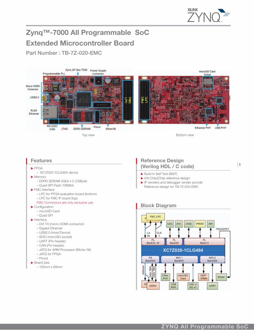
Zynq™-7000 All Programmable SoC
Extended Microcontroller BoardPart Number : TB-7Z-020-EMC
Reference Design (Verilog HDL / C code)EBuild In Self Test (BIST)EAXI Chip2Chip reference design E IP venders and debugger vender provide
Reference design for TB-7Z-020-EMC
Block Diagram
FeaturesEFPGA
– XC7Z020-1CLG484 device EMemory
– DDR3 SDRAM 4Gbit x 2 (1GByte)– Quad SPI Flash 128Mbit
EFMC Interface– LPC for FPGA evaluation board (bottom)– LPC for FMC IF board (top)FMC Connectors are only exclusive use
EConfiguration– microSD Card– Quad SPI
EInterface– DVI TX (micro-HDMI connector)– Gigabit Ethernet– USB2.0 (Host/Device)– SDIO (microSD socket)– UART (Pin-header)– CAN (Pin-header)– JATG for ARM Processor (Mictor 38)– JATG for FPGA– Pmod
EBoard size– 130mm x 69mm
ZYNQ All Programmable SoC
Top view Bottom view

7
KintexTM-7 FPGA ACDC (Acquisition, Contribution, Distribution and Consumption) 1.0 Base BoardPart Number : TB-7K-325T-IMG
Reference Design (Verilog HDL)EHDMI Frame Buffer Design
– HDMI interface design with TB-FMCH-HDMI2 (sold separately) Memory controller : Generated by Memory Interface Generator (MIG)
EEDK Base System Builder Design– XDB file for EDK base system builder– MicroBlazeTM softcore CPU and peripherals
FeaturesEFPGA
– XC7K325T-FFG900 device EMemory
– DDR3 SDRAM (2Gbit) x 4 EFMC Interface*
– HPC (High Pin Count) x 2– LPC (Low Pin Count) x 2
EConfiguration– Via QUAD SPI Flash (128Mbit)
EInterfaces– MMCX for External Clock – JTAG– UART (RS-232C D-sub9pin) – XADC Pin header – DIP Switch, Push button and LED
EBoard size– 240mm x 175mm
* Not all VITA57.1 signals are populated.
Kintex-7 FPGA
8
Kintex-7 FPGA Display KitPart Number : TB-7K-ACDC-FND / TB-7K-ACDC-PRO-TV
Reference Design (Verilog HDL)EBasic Reference design for PRO and FND KIT
• HDMI Frame Buffer :– HDMI Interface (TB-FMCH-HDMI2)– Memory controller :
Memory Interface Generator (MIG) generator
EReference design for PRO KIT only • LVDS reference design • V-by-One® HS reference design with time limitation • EDK :
– EDK Base system builder XDB file – MicroBlaze soft core CPU
FeaturesETB-7K-325T-IMG Base BoardEFMC Interface
– HPC (High Pin Count) x 2– LPC (Low Pin Count) x 2
EISE Design Suite– PRO : Embedded Edition– FND : Logic Edition(Device-locked for the Kintex-7 325T FPGA)
EDocumentation– Hardware Users Manual– Reference Design– Schematics
ECables– Power Supply– Digilent Programming Cable
EPush SW, DIP SW and LED
ETB-7K-ACDC-PRO includes HDMI 2, V-by-One® HS , LVDS FMC Option Cards
ETB-7K-ACDC-FND includes HDMI 2 FMC Option Card
Kintex-7 FPGA
9
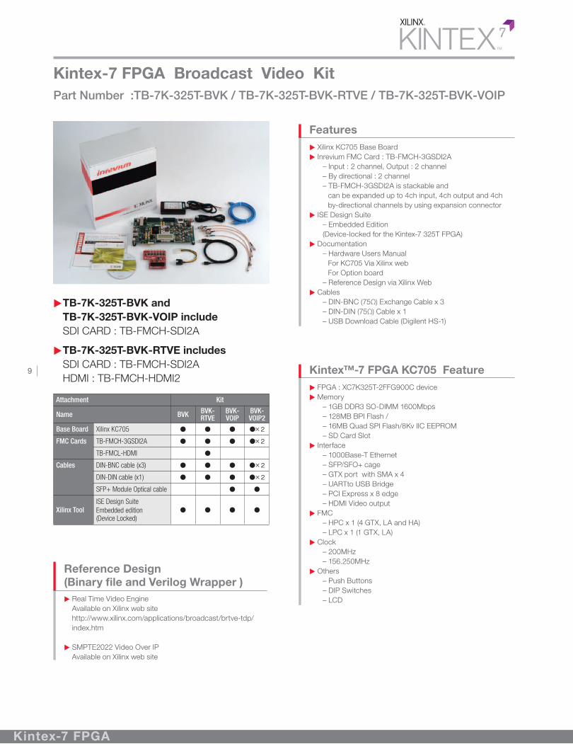
Kintex-7 FPGA Broadcast Video KitPart Number :TB-7K-325T-BVK / TB-7K-325T-BVK-RTVE / TB-7K-325T-BVK-VOIP
Reference Design (Binary file and Verilog Wrapper )E Real Time Video Engine
Available on Xilinx web site http://www.xilinx.com/applications/broadcast/brtve-tdp/index.htm
ESMPTE2022 Video Over IP Available on Xilinx web site
FeaturesEXilinx KC705 Base BoardEInrevium FMC Card : TB-FMCH-3GSDI2A
– Input : 2 channel, Output : 2 channel– By directional : 2 channel– TB-FMCH-3GSDI2A is stackable and
can be expanded up to 4ch input, 4ch output and 4ch by-directional channels by using expansion connector
EISE Design Suite– Embedded Edition(Device-locked for the Kintex-7 325T FPGA)
EDocumentation– Hardware Users Manual
For KC705 Via Xilinx web For Option board
– Reference Design via Xilinx Web ECables
– DIN-BNC (75Ω) Exchange Cable x 3– DIN-DIN (75Ω) Cable x 1– USB Download Cable (Digilent HS-1)
Kintex™-7 FPGA KC705 FeatureEFPGA : XC7K325T-2FFG900C deviceEMemory
– 1GB DDR3 SO-DIMM 1600Mbps– 128MB BPI Flash / – 16MB Quad SPI Flash/8Kv IIC EEPROM– SD Card Slot
EInterface– 1000Base-T Ethernet– SFP/SFO+ cage– GTX port with SMA x 4– UARTto USB Bridge– PCI Express x 8 edge– HDMI Video output
EFMC– HPC x 1 (4 GTX, LA and HA)– LPC x 1 (1 GTX, LA)
EClock– 200MHz– 156.250MHz
EOthers– Push Buttons– DIP Switches– LCD
E TB-7K-325T-BVK and TB-7K-325T-BVK-VOIP include
SDI CARD : TB-FMCH-SDI2A
ETB-7K-325T-BVK-RTVE includes SDI CARD : TB-FMCH-SDI2A HDMI : TB-FMCH-HDMI2
Kintex-7 FPGA
Attachment Kit
Name BVK BVK- RTVE
BVK- VOIP
BVK- VOIP2
Base Board Xilinx KC705 ● ● ● ●×2
FMC Cards TB-FMCH-3GSDI2A ● ● ● ●×2
TB-FMCL-HDMI ●
Cables DIN-BNC cable (x3) ● ● ● ●×2
DIN-DIN cable (x1) ● ● ● ●×2
SFP+ Module Optical cable ● ●
Xilinx ToolISE Design Suite Embedded edition(Device Locked)
● ● ● ●

10
Virtex-7 FPGA
Virtex-7 FPGA PCI Express Gen3 Evaluation PlatformAvailable : Q2 2013
Part Number : TB-7VX690T-PCIEXP / TB-7VX980T-PCIEXP / TB-7VX1140T-PCIEXP
Board specificationEFPGA
– XC7VX690T / XC7VX980T-FFG1926 / XC7VX1140T-FLG1926
FLG1926 and FFG1926 are Pin compatible package
EMemory– DDR3 SDRAM SO-DIMM(8 Gbyte) x 2– QSPI (128M bit)
ESerdes IF through connector – PCI Express (GTH 8 lane)– FMC HPC x 4 (GTH 10 lane)– SMA (GTH 1 lane)
EInterface – FMC HPC x 4– MMCX clock input – External PLL– RS232 (Pin Header)– JTAG – USB3.0
FeaturesESupporting PCI Express Gen3 x 8 EAvailable 2* DDR3 SDRAM SO-DIMM E40ch Rocket IO thorough FMC connector enable total
400Gbps data transfer
Reference Design (Verilog HDL)ESPCI Express DMA Design with Time limitation EMemory controller : 1866Mbps (MIG)EOptical IF loopback design EWindows7 64bit Driver (Binary)EApplication software (Binary)

11
Spartan-6 FPGA
DDR3 and 8ch GTP Spartan®-6 FPGA Evaluation PlatformPart Number : TB-6S-LX150T-IMG2
FeaturesEFPGA
– Xilinx FPGA: XC6SLX150T-3FFG900 device EMemory
– DDR3 SDRAM 1Gbit x 3 EFMC Interface*
– HPC (high pin count) connector x 1– LPC (low pin count) connector x 2
EConfiguration– SPI Flash 128 Mbit
EInterfaces– MMCX clock input– USB to PC (via USB-UART conversion device)– JTAG– DIP Switch, Push button and LED
EBoard size– 240mm x 175mm
* Not all VITA57.1 signals are populated.
Reference Design (Verilog HDL)EHDMI Frame Buffer Design
– HDMI interface design with TB-FMCL-HDMI2 (sold separately)
– Memory controller : 800Mbps, 32bit data width, Generated by Memory Interface Generator (MIG).
EEDK Base System Builder Design– XDB file for EDK base system builder– MicroBlazeTM softcore CPU and peripherals

12
Spartan-6 FPGA Consumer Video Kit 2.0Part Number : TB-6S-CVK2-PRO / TB-6S-CVK2-FND
FeaturesETB-6S-LX150T-IMG2 base board EFMC Option Cards (LVDS, V-by-One® HS, DisplayPort
HDMI1.4a )EISE® Design Suite: Device-locked for the Spartan-6
LX150T FPGAEDocumentation
– Getting Start-up Guide– Hardware Users Manual– Reference Design– Schematics
ECables– Power Supply– Xilinx Platform Cable USB-II– LVDS Cable– MMCX to MMCX/SMA Connectors– V-by-One HS Cable
ETB-6S-CVK2-PRO includes LVDS, V-by-One® HS, DisplayPort®, and
HDMI1.4a FMC Option Cards
ETB-6S-CVK2-FND includes LVDS FMC Option Card
Reference Design (Verilog HDL)ELVDS Design
– 7:1 LVDS loop-back test design with TB-FMCL-LVDSEHDMI1.4 Design
– Frame split and 2ch output Design, 3D Format data (Side-by-Side)
EV-by-One® HS Design– HDMI input to V-by-One HS output Design– V-by-One HS loop-back design
EDisplayPort Reference Design– DisplayPort interface design
(A bitstream data is provided from Xilinx web site for CVK2-PRO)
Spartan-6 FPGA

13
Virtex-6 FPGA
Large Capacity Extendable PCI Express Gen 2 PlatformPart Number : TB-6V-LX550T, and SX475T-PCIEXP
FeaturesEFPGA
– Xilinx FPGA: XC6VL550T/ SX475T-2FFG1759 device EMemory
– DDR3 SDRAM SO-DIMM connector x 2 (1Gbyte SO-DIMM modules supplied)
– SPI Flash 128MbitEPCI Express®
– Gen 2 x 8 (SX475T supported)– Gen 2 x 4 (LX550T supported)
EFMC Interface*– HPC (high pin count) connector x 2– LPC (low pin count) connector x 1
EConfiguration– Configuration from micro-SD card– High-speed configuration from on-board NAND Flash
EInterfaces– MMCX clock input– External PLL– RS-232 (UART)– JTAG– Pin header– DIP Switch, Push button and LED
EBoard size– 300mm x 130mm
Reference Design (Verilog HDL)EHDMI Capturing and PCI express DMA Design
– HDMI interface design for TB-FMCL-HDMI (sold separately)
– Memory controller : 800Mbps, 64bit data width, Generated by Memory Interface Generator (MIG).
– DMA design for PCI Express Gen 2 x 8 (except LX550T version)
– Driver software for Windows 7 / XP, 32bit. (.exe file only)– Application software (.exe file only)
Backside
* Not all VITA57.1 signals are populated.
Application Software GUI

14
FMC Cards
Platform Part Number
FMC Card Part Number
Virtex-7 FPGA Kintex-7 FPGA Virtex-6 FPGA Spartan-6 FPGA
TB-7V-2000T-LSI TB-7K-325T-IMG TB-6V-LX760-LSI TB-6V-xxxxT-PCIEXP
TB-6S-LX150T-IMG2
FMC
(TB-FMCL-xx)
LVDS ●※1 ◎ ● ● ◎
INET ●※1 ● ● ● ◎
L-PH ●※1 ● ● ● ●
USB30 ●※1 ◎ ● ● ◎
GLAN-B ●※1 ● ● ● ◎
AUDIO ●※1 ● ● ● ●
ADDA24 ●※1 ● ● ● ◎
TB-72-020-EMC ◎※1 ◎ ● ● ●
(TB-FMCH-xx)
DP ●
VBY1 ●※2 ◎ ◎
HDMI2 ●※1 ◎ ● ● ◎
3GSDI2A ● ● ●
H-PH ● ● ● ●
※ 1 Please use the included conversion board.
※ 2 Direct connection to onboard FMC
◎ : Reference design is available.
FMC Option Cards table
15
FMC Cards
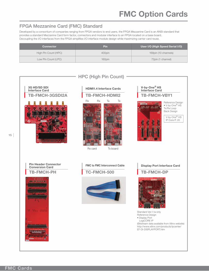
Rx
Rx card Tx board
Rx Tx TxReference Design• V-by-One® HSTx/Rx Loop Back Design
V-by-One® HSIP Core P. 20
FMC Option Cards
TC-FMCH-500
Pin Header Connector Conversion Card
TB-FMCH-PH
HPC (High Pin Count)
3G HD/SD SDI Interface Card
TB-FMCH-3GSDI2A
TB-FMCH-HDMI2
V-by-One® HS Interface Card
TB-FMCH-VBY1
HDMI1.4 Interface Cards
FMC to FMC Interconnect Cable
FPGA Mezzanine Card (FMC) StandardDeveloped by a consortium of companies ranging from FPGA vendors to end users, the FPGA Mezzanine Card is an ANSI standard that provides a standard Mezzanine Card form factor, connectors and modular interface to an FPGA located on a base board. Decoupling the I/O interfaces from the FPGA simplifies I/O interface module design while maximizing carrier card reuse.
Connector Pin User I/O (High Speed Serial I/O)
High Pin Count (HPC) 400pin 168pin (10 channels)
Low Pin Count (LPC) 160pin 72pin (1 channel)
Standard Ver.1.1a onlyReference Design• Display Port LogiCORE IP(Bitstream data available from Xilinx website)http://www.xilinx.com/products/ipcenter/EF-DI-DISPLAYPORT.htm
TB-FMCH-DP
Display Port Interface Card

16
FMC Cards
Reference Design• LVDS Tx/Rx Loop Back Design (VerilogHDL)
Gigabit Ethernet x2 port (PoE)1000 Base-TPHY Chip (Marvell)88E1111-B2-BAB1C000
Input: 2chOutput: 2ch
CYPRESS: CYUSB3014
FMC Option Cards
Zynq-7000 All Programmable Soc Extension Microcontroller Card
TB-7Z-020-EMC
Pin Header Connector Conversion Cards
TB-FMCL-PH
24bit/192KHz AD/DA Audio Interface Card
TB-FMCL-ADDA24
LPC (Low Pin Count)
USB3.0 Device Interface Card
TB-FMCL-USB30
TB-FMCL-LVDS
1000 Base-T Ethernet Interface Card
TB-FMCL-GLAN-B
100 Base Ethernet Interface Card
TB-FMCL-INET
TB-FMCL-AUDIO
LVDS Interface Card
AES3 Audio Interface Card

17
Application Specific Solution
Application Specific Solution
TED provides audio application platform with 3rd party’s network IP for network audio.This solution provides real time audio transfer via 100 base Ethernet and reduce cables.
Spartan-6 FPGA Network Audio platform
Audio PlatformELow Cost Platform
– TB-6S-LX25-NAP EHigh Performance Platform
– TB-6S-LX150T-IMG2 (Spartan-6 FPGA)– TB-FMCL-GLAN-B (10/100/1000Base Ethernet)– TB-FMCL-ADDA24 (Analog Audio IF)
TB-6S-LX25-NAP FeatureE24bit / 192KHz high quality AD/DA converterE4ch line input/4ch line output (+4dBu/-10dBV)ESPDIF digital audio interface In/outE100 base Ethernet x 2chESpartan-6 FPGA LX25 DeviceEOn board VCXO
TB-FMCL-ADDA24 FeatureE24bit / 192KHz high quality AD/DA converterE4ch line input/4ch line output (+4dBu/-10dBV)EOn board VCXO
TB-6S-LX25-NAP
Low Cost Boards
High PerformanceBoards
TB-FMCL-GLAN-B
TB-FMCL-ADDA24
TB-6S-LX150T-IMG2
18
Application Specific Solution
Application Specific Solution
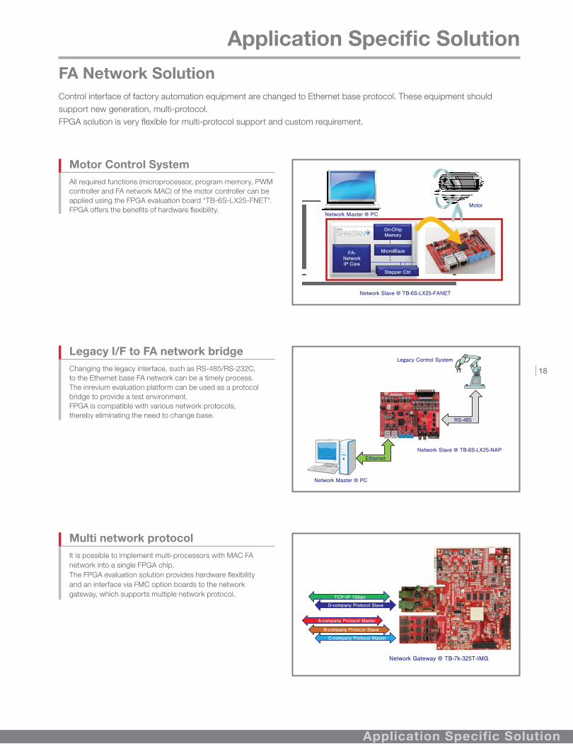
Control interface of factory automation equipment are changed to Ethernet base protocol. These equipment should support new generation, multi-protocol.FPGA solution is very flexible for multi-protocol support and custom requirement.
FA Network Solution
Motor Control SystemAll required functions (microprocessor, program memory, PWM controller and FA network MAC) of the motor controller can be applied using the FPGA evaluation board “TB-6S-LX25-FNET”.FPGA offers the benefits of hardware flexibility.
Legacy I/F to FA network bridgeChanging the legacy interface, such as RS-485/RS-232C, to the Ethernet base FA network can be a timely process. The inrevium evaluation platform can be used as a protocol bridge to provide a test environment.FPGA is compatible with various network protocols, thereby eliminating the need to change base.
Multi network protocolIt is possible to implement multi-processors with MAC FA network into a single FPGA chip.The FPGA evaluation solution provides hardware flexibility and an interface via FMC option boards to the network gateway, which supports multiple network protocol.
Ctrl
Network Master @ PC
Network Slave @ TB-6S-LX25-FANET
Motor
FA-NetworkIP Core
MicroBlaze
Stepper Ctrl
On-ChipMemory
Network Master @ PC
Network Slave @ TB-6S-LX25-NAPEthernet
RS-485
Legacy Control System
A-company Protocol Master
B-company Protocol Slave
C-company Protocol Master
TCP/IP 1Gbps
D-company Protocol Slave
Network Gateway @ TB-7k-325T-IMG

19
Original IP Core
MECHATROLINK-III Master/Slave IP Core MECHATROLINK-III is highly suited to networks that emphasize precise, synchronous control and high speeds. MECHATROLINK-III was developed by the MECHATROLINK Members Association as a standard to satisfy the demands of the motion field network market. It boasts higher transmission speeds, faster transmission cycle times and greater transmission distances than ever before, as well as a higher number of maximum slaves.
Features
EMaster / Slave Function
EDelivers single chip intelligent function control using FPGA soft-processor with RTOS
EMAX 66MHz Clock, High-speed, Synchronous host interface
EFlexible system configuration by FPGA Logic fabric– 16bit/8bit CPU buss, asynchronous buss – Zynq AP SoC or Microblaze base SoC
Core Specifications
ENetwork: MECHATROLINK-III Network ×2 (Port For MII
interface 100Mbps Full Duplex mode)
EHost interface: 32bit Joint memory interface / 32bit
register interface
E Interrupt: 2 interrupt output
EBit ordering: little endian
EDeliverable style: Netlist
System Configuration Diagram
Target Device
ESpartan-6 FPGA Family
Function specifications MECHATROLINK-III
Physical layer Ethernet
Transmission cycle time 31.25 µs to 64 ms*
String size 8/16/32/48/64 bytes (Different string sizes can be used at the same time)
Number of slaves 62 max
Maximum transmission distance 100 m between stations 0.5m
Minimum distance between stations 0.2 m
Message communications Available
Original IP Core

20
V-by-One HS IP CoreFor Kintex-7 FPGA Project License For Artix-7 FPGA Project License TX IP : TIP-VBY1HS-K7TX-PROJ TX IP : TIP-VBY1HS-A7TX-PROJ RX IP : TIP-VBY1HS-K7RX-PROJ RX IP : TIP-VBY1HS-A7RX-PROJ TX-RX IP : TIP-VBY1HS-K7-PROJ TX-RX IP : TIP-VBY1HS-A7-PROJPlease contact us for Part number of Spartan-6 & Vitrex-6 & Virtex-7 FPGA
The V-by-One®HS standard has been developed by THine Electronics Inc. to offer capabilities for FPD markets that require ever-higher frame rates and resolutions. Tokyo Electron Device (TED) offers V-by-One®HS IP Core for Xilinx FPGA, reducing costs, time to market and number of cable pairs required.
Features
ETargets high-speed video signal transmission based on internal connection of equipment.
EUp to 3.75Gbps data rate (effective data rate 3Gbps) per lane.
EData scrambling and Clock Data Recovery (CDR) to reduce EMI.
ECDR solves the skew problem between clock and data in conventional transfer systems.
Core Specifications
EUp to 3.75Gbps data rate per lane on Virtex®-6
(Up to 3.125Gbps on Spartan®-6)
E1-, 2-, 4- and 8-lane operation
(Design service for 16 and 32 lanes is available.)
EVariable settings of driver swing, pre-emphasis and
equalizer.
EFlexible implementation and package compatibility.
Link System Diagram
Resolution Refresh rate (Pixel Clock) Color depth1) No. of Data Lane
HD
60Hz (74.25MHz)
18/24/30/36 bit
1
120Hz (148.5MHz) 2
240Hz (297MHz) 4
Full-HD
60Hz (148.5MHz)
18/24/30/36 bit
2
120Hz (297MHz) 4
240Hz (594MHz) 8
4Kx2K
60Hz (594MHz)
18/24/30/36 bit
8
120Hz (1188MHz) 162)
240Hz (2376MHz) 322)
1) IP Core support of color depth & data lanes depends on the target FPGA service.2) Design service for 16 or 32 lanes is available.
Target DevicesCore resources of the reference design that has 4-data lanes is shown in the following table. So the smallest devices are available to implement the design including the core.
Spartan®-6 FPGA Family : XC6SLX25T (Slices: 30%)
Virtex®-6 FPGA Family : XC6VLX75T (Slices: 10%)
Original IP Core
Original IP Core

21
Design Service
High-Speed serial IO• PCI Express GEN1/GEN2 ×4 to ×16 Lane• PCI Express GEN3 ×8• Serial Rapid IO • 1G/10G EthernetMemory controller• DDR2 SDRAM • DDR3 SDRAMImage processing• CameraLink(Full/Base) • V-by-One HS • HDMI • DVIIO• CameraLink(Full/Base) • V-by-One HS • HDMI • DVI
Design ServiceTED’s Design Center boasts a record of over 200 significant development innovations a year. We leverage the design knowledge acquired here to provide our customers with optimized design and development services covering every area from hardware design to the latest technical information from our suppliers, enabling us to engage in even the most complex leading-edge development projects.
Development
Customize
OEM
Design Service
Figures of development for 2012 Key Technology
Sensing part
Data correcting Data processing (PC/server)
Camera Sensor
Grabber boardFPGA: Image processingDDR3: SDRAM
Optical moduleSFP/SFP+
Interface boardFPGA Data transferDDR3 SDRAM
Mother boardProcessorI.MAX
Metal/Optical �ber IOPC
High-Speed Serial I/F IOImage processing I/F
CameraLink, DVI, V-by-One, HDMI Serial Rapid IO
Coordinated to meet customer requests
PCI Express, 1G/10G Ethernet USB2.0/3.0, SATA
Customer requests (Design order)
Development
Technical review Preproduction
Part selection Part procurement
Production model
EV-by-One HS® IP lane expansion from 8ch to 32ch (8ch x 4) EAdding image data import design by DDR3 memory controller ECombine two existing boards and create brand new board with
two FPGA
IP Customize Example
V‐by‐One HSIP
V‐by‐One HSIP
8
8
8
8
8
DDR3 SDRAM
DDR3 MemoryController
8 lanes 32 lanes&
Addmemory controller
DesignService
Board Customize
DesignService
Board Customize Example

22
World HeadquartersPLD Solution Dept. Yokohama, JapanTEL: +81-45-443-4034E-mail: [email protected] http://www.inrevium.jp/eng
North America3100 W. Warren Avenue, Fremont, CA 94538TEL: +1-510-624-3457E-mail: [email protected]
KOREATOKYO ELECTRON DEVICE KOREA OFFICERoom No.427, 4/F., Haesung Building 942, Daechi-dong, Gangnam-gu, Seoul, 135-845, KoreaTEL: +82-2-6004-1331
ShanghaiNo. 402, 4F, Building 2, Lujiazui Software Park No. 100, Lane 91, E Shan Rd, Pudong District, Shanghai, China 200127TEL: +86-21-6132-9626 E-mail: [email protected] http://www.teldevice.cn
TAIWANTOKYO ELECTRON DEVICE TAIWAN OFFICE No.7, Dusing Rd., Hsinchu Science Park, Hsinchu City 30078, Taiwan, R.O.C.TEL: +886-3-666-2266 Fax: +886-3-666-2277
SINGAPORETOKYO ELECTRON DEVICE SINGAPORE PTE. LTD. 175A Bencoolen Street #05-01/02 Burlington Square Singapore 189650TEL: +65-6542-1776http://www.teldevice.co.jp/eng/company/singapore.html
UKTokyo Electron Europe Ltd.Pioneer, Crawley Business Quarter Fleming Way, Crawley West Sussex, RH10 9QL, UKTEL: +44-1293-655807
Contact
Tokyo Electron Device markets proprietary information, technology and services under our original ‘inrevium’ brand name. The name was created by combining the first letters of the words ‘intellectual’ and ‘revolutionary’, with the suffix ‘-ium’ (‘element’) added. It signifies our ongoing mission to help solve customer problems and aid their business activities through our groundbreaking proprietary information, technology and services.
Tokyo Electron Device’s electronic component business has been certified for ISO14001 by Japan Audit and Certification Organization for Environment and Quality (JACO).
Names of companies, products and services in this pamphlet are trademarks or registered trademarks of their respective owners.
Local
Contact