Embed Size (px)
Citation preview

Cool Solutions for Wireless Connectivity
XEMICS SA • e-mail: [email protected] • web: www.xemics.com
Data Sheet XE1202
XE1202
433MHz / 868MHz / 915MHz
Low-power, integrated UHF transceiver GENERAL DESCRIPTION The XE1202 is a single chip transceiver operating in the 433, 868 and 915MHz license free ISM (Industry Scientific and Medical) frequency bands. Its highly integrated architecture allows for minimum external components while maintaining design flexibility. All major RF communication parameters are programmable and most of them can be dynamically set. The XE1202 offers the unique advantage of narrow-band and wide-band communication, this without the need to modify the number or parameters of the external components. The XE1202 is optimized for low power consumption while offering high RF output power and channelized operation suited for both the European (ETSI-300-220) and the North American (FCC part 15) regulatory standards APPLICATIONS • Narrow-band and wide-band security systems
• Voice and data over an RF link
• Process and building control
• Access control
• Home automation
• Home appliances interconnection
KEY PRODUCT FEATURES • Programmable RF output power: up to +15dBm • High reception sensitivity: down to –116dBm • Low power consumption: RX=14mA; TX = 48mA
@15 dBm output power • Supply voltage down to 2.4V • Wide band operation: 400kHz channels for data
rates of up to 76.8kbps, NRZ coding • Narrow band operation: down to 25kHz channels
for data rates of 4.8kbps, NRZ coding • On-chip frequency synthesizer with steps of 500Hz • Continuous phase 2-level FSK modulation • Incoming data pattern recognition • Built-in Bit-Synchronizer for incoming data and
clock synchronization and recovery • RSSI (Received Signal Strength Indicator) and FEI
(Frequency Error Indicator)
ORDERING INFORMATION Part number Temperature range Package XE1202I027 -40°C to +85° LQFP44
PA VCO PFDmodulator
/n Synthesizer
Oscillator /nClock Out
POR
I Ref
ControlLogic
PatternRecognition
RSSI FEIPhaseShifter
LOBuff.
LNA
AMP
AMP
BPF
BPF
AMP
AMP Limiter
Limiter
FSKDemod.
BitSync.
QAmpIAmp
I
Q
DCLK
DATAOUT
PATTERN
MODE 0
MODE 1
MODE 2
SI
SO
SCK
EN
DATAIN
RFA
VDD
VDD
A
VDD
D
VDD
F
VDD
P
IAM
P
QAM
P
RFB
RFOUT
TKA
TKB
LFB
XTA
XTB
CLK
OU
T
VSSD
VSSF
VSSP
VSSP
VSSF
VSSA VS
S
VSSA
TVC
O
TSU
PP
SCAN
Prog.divider
2 D0306-105
Data Sheet XE1202
TABLE OF CONTENTS
General Description.................................................................................................................................................. 1 Applications .............................................................................................................................................................. 1 Key product features ................................................................................................................................................ 1 Ordering information................................................................................................................................................. 1 1 Functional Block Diagram .............................................................................................................................. 3 2 Pin description ................................................................................................................................................ 4 3 Electrical Characteristics ............................................................................................................................... 5 3.1 Absolute Maximum Operating Ranges.......................................................................................................... 5 3.2 Specifications................................................................................................................................................. 5 3.2.1 Operating Range .......................................................................................................................................... 5 3.2.2 Electrical Specifications ................................................................................................................................ 5 4 Description....................................................................................................................................................... 7 4.1 Detailed description ....................................................................................................................................... 8 4.1.1 Receiver........................................................................................................................................................ 8 4.1.2 High sensitivity vs. high linearity: A-mode, B-mode...................................................................................... 9 4.1.3 RSSI.............................................................................................................................................................. 9 4.1.4 Frequency Error Indicator - FEI .................................................................................................................. 10 4.1.5 Transmitter.................................................................................................................................................. 12 4.1.6 Pattern recognition...................................................................................................................................... 13 4.1.7 Frequency synthesizer................................................................................................................................ 13 5 Interface definition, Principles of operation............................................................................................... 14 5.1 Serial Control Interface................................................................................................................................ 14 5.2 Configuration and Status registers .............................................................................................................. 15 5.2.1 RTParam configuration register.................................................................................................................. 15 5.2.2 FSParam configuration register .................................................................................................................. 17 5.2.3 DataOut register ......................................................................................................................................... 18 5.2.4 ADParam configuration register ................................................................................................................. 18 5.2.5 Pattern register ........................................................................................................................................... 19 5.3 Operating Modes ......................................................................................................................................... 20 5.4 Transmitted Data Interface .......................................................................................................................... 22 5.5 Received Data Interface .............................................................................................................................. 22 5.6 Pattern Recognition Interface ...................................................................................................................... 22 5.7 Clock Output Interface................................................................................................................................. 23 5.8 Default settings at power-up........................................................................................................................ 23 6 Application Information................................................................................................................................ 24 6.1 Matching network of the receiver................................................................................................................. 24 6.2 Matching network of the transmitter ............................................................................................................ 24 6.3 VCO tank ..................................................................................................................................................... 25 6.4 Loop filter of the frequency synthesizer....................................................................................................... 25 6.5 Reference crystal for the frequency synthesizer ......................................................................................... 26 7 Packaging information.................................................................................................................................. 27

3 D0306-105
Data Sheet XE1202
The XE1202 single-chip solution is an integrated circuit intended for use as a low cost FSK transceiver to establish a frequency-agile, half-duplex, bi-directional RF link, with non-return to zero data coding. The device is available in an LQFP44 package and is designed to provide a fully functional multi-channel FSK transceiver. It is intended for applications in the 433- and 868MHz European band and the North American 902-928MHz ISM band. The single chip transceiver operates down to 2.4 V and provides low power consumption solutions for battery-operated and power sensitive applications. Thanks to the low external components count, the XE1202 is ideal for small size, low-cost UHF links. Its reference board design has no tunable components, which facilitates high volume cost sensitive production. The XE1202 can easily be interfaced to a controller such as the XEMICS’ XE8000 Series of ultra low-power microcontrollers. The XE1202 serial control registers are programmed by the MCU and the MCU manages the communication protocol.
1 Functional Block Diagram
PA VCO PFDmodulator
/n Synthesizer
Oscillator /nClock Out
POR
I Ref
ControlLogic
PatternRecognition
RSSI FEIPhaseShifter
LOBuff.
LNA
AMP
AMP
BPF
BPF
AMP
AMP Limiter
Limiter
FSKDemod.
BitSync.
QAmpIAmp
I
Q
DCLK
DATAOUT
PATTERN
MODE 0
MODE 1
MODE 2
SI
SO
SCK
EN
DATAIN
RFA
VDD
VDD
A
VDD
D
VDD
F
VDD
P
IAM
P
QAM
P
RFB
RFOUT
TKA
TKB
LFB
XTA
XTB
CLK
OU
T
VSSD
VSSF
VSSP
VSSP
VSSF
VSSA VS
S
VSSA
TVC
O
TSU
PP
SCAN
Prog.divider
4 D0306-105
Data Sheet XE1202
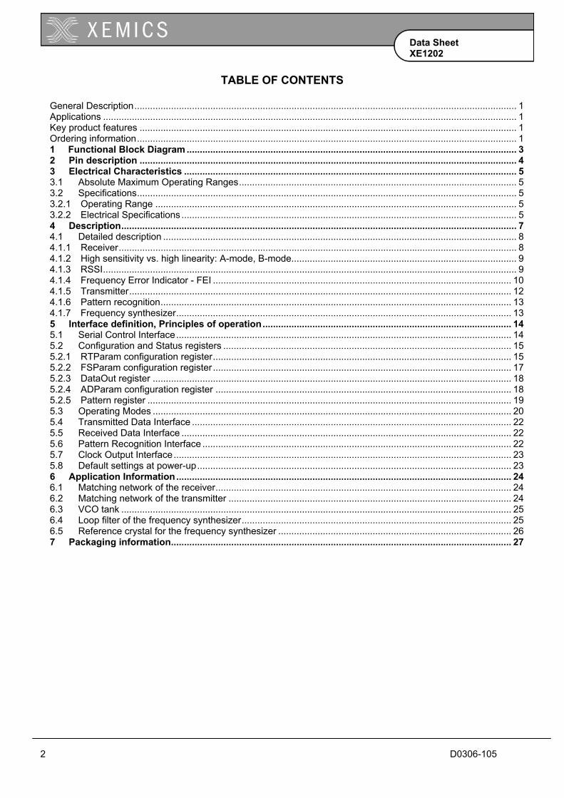
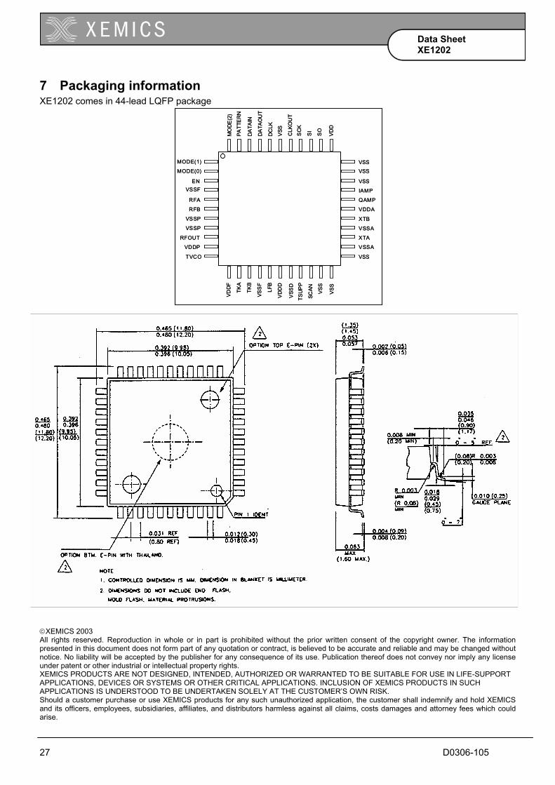
2 Pin description PIN NAME DESCRIPTION 1 MODE(1) In Transmit/Receive/Stand-by/Sleep Mode Select 2 MODE(0) In Transmit/Receive/Stand-by/Sleep Mode Select 3 EN In Chip Enable 4 VSSF HF Analog Ground 5 RFA In RF Input 6 RFB In RF Input 7 VSSP In Power Amplifier Ground 8 VSSP In Power Amplifier Ground 9 RFOUT Out RF Output 10 VDDP Power Amplifier Supply Voltage 11 TVCO In Test Input (connected to VSS in normal operation) 12 VDD HF Analog Supply Voltage 13 TKA I/O VCO Tank 14 TKB I/O VCO Tank 15 VSSF HF Analog Ground 16 LFB I/O PLL Loop Filter 17 VDDD HF Digital Supply Voltage 18 VSSD HF Digital Ground 19 TSUPP Test Circuit Supply Voltage (connected to VSS in normal operation) 20 SCAN In Scan Test Input (connected to VSS in normal operation) 21 OPT (connected to VSS in normal operation) 22 TMOD[0] (connected to VSS in normal operation) 23 TMOD[1] (connected to VSS in normal operation) 24 VSSA LF Analog Ground 25 XTA I/O Ref Xtal / Input of external clock 26 VSSA LF Analog Ground 27 XTB I/O Reference Xtal 28 VDDA LF Analog Supply Voltage 29 QAMP Out Output of Q low-pass filter 30 IAMP Out Output of I low-pass filter 31 TMOD[2] (connected to VSS in normal operation) 32 TMOD[3] (connected to VSS in normal operation) 33 TIBIAS (connected to VSS in normal operation) 34 VDD LF Digital Supply Voltage 35 SO Out Configuration Register Serial Output 36 SI In Configuration Register Serial Input 37 SCK In Configuration Register Serial Clock 38 CLKOUT Out Output clock at reference frequency divided by 4, 8, 16 or 32 39 VSS LF Digital Ground 40 DCLK Out Recovered Received Data Clock 41 DATAOUT Out Received Data 42 DATAIN In Transmit Data 43 PATTERN Out Output of the pattern recognition block 44 MODE(2) In Transmit/Receive/Stand-by/Sleep Mode Select
5 D0306-105
Data Sheet XE1202
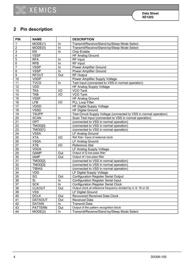
3 Electrical Characteristics
3.1 Absolute Maximum Operating Ranges Stresses above those values listed below may cause permanent device failure. Exposure to absolute maximum ratings for extended periods may affect device reliability.
Symbol Description Min. Max. Unit VDDmr Supply voltage -0.5 3.9 V Tmr Storage temperature -55 125 °C
The device is ESD sensitive and should be handled with precaution.
3.2 Specifications 3.2.1 Operating Range
Symbol Description Min. Max. Unit VDDop Supply voltage 2.4 (*) 3.6 V TRop Temperature -40 85 °C CLop Load capacitance on digital ports - 25 pF
(*) For narrow-band configurations (base-band filter bandwidths of 10, 20 and 40 kHz), the minimum operating supply voltage is 2.4 V. For 200kHz base-band filter bandwidth setting the minimum operating supply voltage is 2.7V.
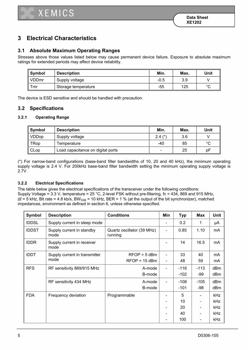
3.2.2 Electrical Specifications The table below gives the electrical specifications of the transceiver under the following conditions: Supply Voltage = 3.3 V, temperature = 25 °C, 2-level FSK without pre-filtering, fc = 434, 869 and 915 MHz, ∆f = 5 kHz, Bit rate = 4.8 kb/s, BWSSB = 10 kHz, BER = 1 % (at the output of the bit synchronizer), matched impedances, environment as defined in section 6, unless otherwise specified.
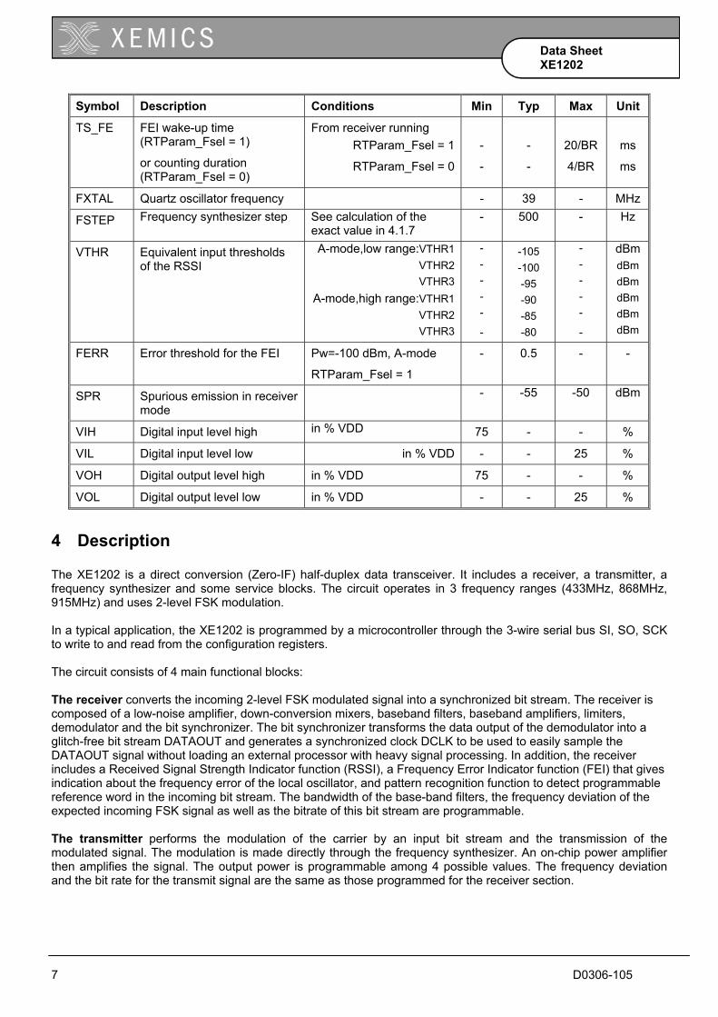
Symbol Description Conditions Min Typ Max Unit
IDDSL Supply current in sleep mode - 0.2 1 µA
IDDST Supply current in standby mode
Quartz oscillator (39 MHz) running
- 0.85 1.10 mA
IDDR Supply current in receiver mode
- 14 16.5 mA
IDDT Supply current in transmitter mode
RFOP = 5 dBm RFOP = 15 dBm
- -
33 48
40 59
mA mA
RF sensitivity 869/915 MHz A-mode B-mode
- -116 -102
-113 -99
dBm dBm
RFS
RF sensitivity 434 MHz A-mode B-mode
- -108 -101
-105 -98
dBm dBm
FDA Frequency deviation Programmable
- - - - -
5 10 20 40
100
- - - - -
kHz kHz kHz kHz kHz

6 D0306-105
Data Sheet XE1202
Symbol Description Conditions Min Typ Max Unit
CCR Co-channel rejection -13 -10 - dBc
IIP3 Input intercept point (from LNA input to base-band filter output)
funw = fLO + 50 kHz and fLO + 95 kHz A-mode B-mode
-43 -28
-40 -25
-
dBm dBm
ML Receiver input level - - -5 dBm
BW Base band filter bandwidth Programmable - - - -
10 20 40
200
- - - -
kHz kHz kHz kHz
Adjacent channel rejection 869 / 915 MHz
funw = fLO + 65 kHz Pw=-107 dBm, A-mode
45 48 - dBc ACR
Adjacent channel rejection 434 MHz
funw = fLO + 65 kHz Pw=-102 dBm, A-mode
42 45 - dBc
BR Bit rate Programmable
- - - - -
4.8 9.6
19.2 38.4 76.8
- - - - -
kb/s kb/s kb/s kb/s kb/s
RFOP RF output power Programmable RFOP10 RFOP1
RFOP20 RFOP2
-3 +2 +7 +12
0
+5 +10 +15
- - - -
dBm dBm dBm dBm
FR Synthesizer frequency range Programmable Each range with its own external components
433 868 902
- - -
435 870 928
MHz MHz MHz
TS_BBR Receiver BB processing wake-up time (first step)
From quartz oscillator running
- 200 250 µs
TS_TR Transmitter wake-up time From frequency synthesizer running
- 100 150 µs
TS_FS Frequency synthesizer wake-up time
From quartz oscillator running
- 200 250 µs
TS_BB2 Receiver RF Front-End wake-up time
From frequency synthesizer running RTParam_WBB=0
- 500 600 µs
TS_FSW Frequency synthesizer switching time
Between 2 channels at 1 MHz from each other
100 150 µs
If RSSI is switched on during mode 010 0.5 ms before switching to mode 100 (see figure 8)
- - 1.0 ms TS_RS RSSI wake-up time (from whole receiver running in mode 100)
If RSSI is switched on during mode 100
- - 1.5 ms
TS_OS Quartz oscillator wake-up time
- 1 2 ms
7 D0306-105
Data Sheet XE1202
Symbol Description Conditions Min Typ Max Unit
TS_FE FEI wake-up time (RTParam_Fsel = 1)
or counting duration (RTParam_Fsel = 0)
From receiver running RTParam_Fsel = 1
RTParam_Fsel = 0
-
-
-
-
20/BR
4/BR
ms
ms
FXTAL Quartz oscillator frequency - 39 - MHz
FSTEP Frequency synthesizer step See calculation of the exact value in 4.1.7
- 500 - Hz
VTHR Equivalent input thresholds of the RSSI
A-mode,low range:VTHR1 VTHR2 VTHR3
A-mode,high range:VTHR1 VTHR2 VTHR3
- - - - -
-
-105 -100 -95 -90 -85 -80
- - - - -
-
dBm dBm dBm dBm dBm dBm
FERR Error threshold for the FEI Pw=-100 dBm, A-mode
RTParam_Fsel = 1
- 0.5 - -
SPR Spurious emission in receiver mode
- -55 -50 dBm
VIH Digital input level high in % VDD 75 - - %
VIL Digital input level low in % VDD - - 25 %
VOH Digital output level high in % VDD 75 - - %
VOL Digital output level low in % VDD - - 25 %
4 Description The XE1202 is a direct conversion (Zero-IF) half-duplex data transceiver. It includes a receiver, a transmitter, a frequency synthesizer and some service blocks. The circuit operates in 3 frequency ranges (433MHz, 868MHz, 915MHz) and uses 2-level FSK modulation. In a typical application, the XE1202 is programmed by a microcontroller through the 3-wire serial bus SI, SO, SCK to write to and read from the configuration registers. The circuit consists of 4 main functional blocks: The receiver converts the incoming 2-level FSK modulated signal into a synchronized bit stream. The receiver is composed of a low-noise amplifier, down-conversion mixers, baseband filters, baseband amplifiers, limiters, demodulator and the bit synchronizer. The bit synchronizer transforms the data output of the demodulator into a glitch-free bit stream DATAOUT and generates a synchronized clock DCLK to be used to easily sample the DATAOUT signal without loading an external processor with heavy signal processing. In addition, the receiver includes a Received Signal Strength Indicator function (RSSI), a Frequency Error Indicator function (FEI) that gives indication about the frequency error of the local oscillator, and pattern recognition function to detect programmable reference word in the incoming bit stream. The bandwidth of the base-band filters, the frequency deviation of the expected incoming FSK signal as well as the bitrate of this bit stream are programmable. The transmitter performs the modulation of the carrier by an input bit stream and the transmission of the modulated signal. The modulation is made directly through the frequency synthesizer. An on-chip power amplifier then amplifies the signal. The output power is programmable among 4 possible values. The frequency deviation and the bit rate for the transmit signal are the same as those programmed for the receiver section.

8 D0306-105
Data Sheet XE1202
The frequency synthesizer generates the local oscillator (LO) signal for the receiver section as well as the FSK modulated signal for the transmitter section. The core of the synthesizer is implemented with a PLL structure. The frequency is programmable with a step of 500 Hz in 3 frequency bands, 433-, 868-, and 915-MHz. This section includes a crystal oscillator whose signal is the reference for the PLL. This reference frequency is divided by 4, 8, 16, or 32 and is made available at the CLKOUT pin to serve as a clock signal for an external processor. The control block generates the control signals according to the setting in its set of configuration registers. The service block performs all the necessary functions for the circuit to work properly, including the internal voltage and current sources.
4.1 Detailed description
4.1.1 Receiver The outputs of the receiver are the two signals DATAOUT and DCLK. When the bit “RTParam_Bits” is “1” (see the Configuration register section below), the bit synchronizer is turned on, and the two output signals are respectively the output NRZ bit stream and the sampling clock. The function of the bit synchronizer is to remove the glitches from the bit stream DATAOUT and to provide the output clock DCLK. The value of DATAOUT is valid at the rising edge of DCLK. For proper behavior of the bit synchronizer, three conditions must be satisfied:
- the received data must start with a preamble of 24 bits for synchronization; this preamble must be a sequence of “0” and “1” sent alternatively,
- after that, the incoming bit stream must have at least one transition from “0” to “1” or from “1” to “0” every 8 bits,
- the accuracy of the bit rate must be better than ± 5 % (assuming the reference Xtal oscillator is exactly 39 MHz)
When “RTParam_Bits” is “0”, the bit synchronizer is turned off, and the signal DATAOUT is the output of the demodulator. In this case DCLK is not used and its value is set to “low”. The condition on the modulation index for proper behavior of the demodulator is:
,22 ≥= ∆⋅BRfβ
where ∆f is the frequency deviation and BR the bit rate. The table below gives the sensitivity for different bit rates, frequency deviations and filter bandwidths.
Sensitivity for BER = 1 % [dBm]
Bit rate [kb/s]
∆f [kHz]
BW [kHz]
mode A mode B 5 10 -116 -102 4.8
20 40 -117 -104 10 20 -115 -101 9.6 20 40 -115.5 -102.5 20 40 -112.5 -99.5 19.2 40 200 -109 -97.5 40 200 -107 -95 38.4 100 200 -109 -97.5
76.8 100 200 -106.5 -95 Table 1 Sensitivity for BER=1 % for different parameter values
9 D0306-105
Data Sheet XE1202
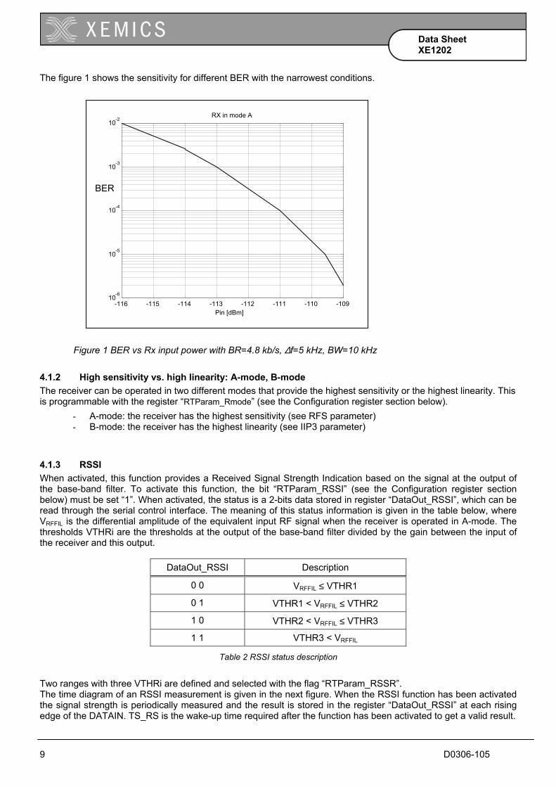
The figure 1 shows the sensitivity for different BER with the narrowest conditions.
Figure 1 BER vs Rx input power with BR=4.8 kb/s, ∆f=5 kHz, BW=10 kHz
4.1.2 High sensitivity vs. high linearity: A-mode, B-mode The receiver can be operated in two different modes that provide the highest sensitivity or the highest linearity. This is programmable with the register “RTParam_Rmode” (see the Configuration register section below).
- A-mode: the receiver has the highest sensitivity (see RFS parameter) - B-mode: the receiver has the highest linearity (see IIP3 parameter)
4.1.3 RSSI When activated, this function provides a Received Signal Strength Indication based on the signal at the output of the base-band filter. To activate this function, the bit “RTParam_RSSI” (see the Configuration register section below) must be set “1”. When activated, the status is a 2-bits data stored in register “DataOut_RSSI”, which can be read through the serial control interface. The meaning of this status information is given in the table below, where VRFFIL is the differential amplitude of the equivalent input RF signal when the receiver is operated in A-mode. The thresholds VTHRi are the thresholds at the output of the base-band filter divided by the gain between the input of the receiver and this output.
DataOut_RSSI Description
0 0 VRFFIL ≤ VTHR1
0 1 VTHR1 < VRFFIL ≤ VTHR2
1 0 VTHR2 < VRFFIL ≤ VTHR3
1 1 VTHR3 < VRFFIL
Table 2 RSSI status description
Two ranges with three VTHRi are defined and selected with the flag “RTParam_RSSR”. The time diagram of an RSSI measurement is given in the next figure. When the RSSI function has been activated the signal strength is periodically measured and the result is stored in the register “DataOut_RSSI” at each rising edge of the DATAIN. TS_RS is the wake-up time required after the function has been activated to get a valid result.
-116 -115 -114 -113 -112 -111 -110 -109 10 -6
10 -5
10 -4
10 -3
10 -2 RX in mode A
Pin [dBm]
BER

10 D0306-105
Data Sheet XE1202
Figure 2 RSSI measurement timing diagram
For applications where the time needed to get the first right result from the RSSI has to be as low as possible, this time can be minimized by waking up the RSSI during mode 010 instead of 100 (see the definition of TS_RS in page 6).
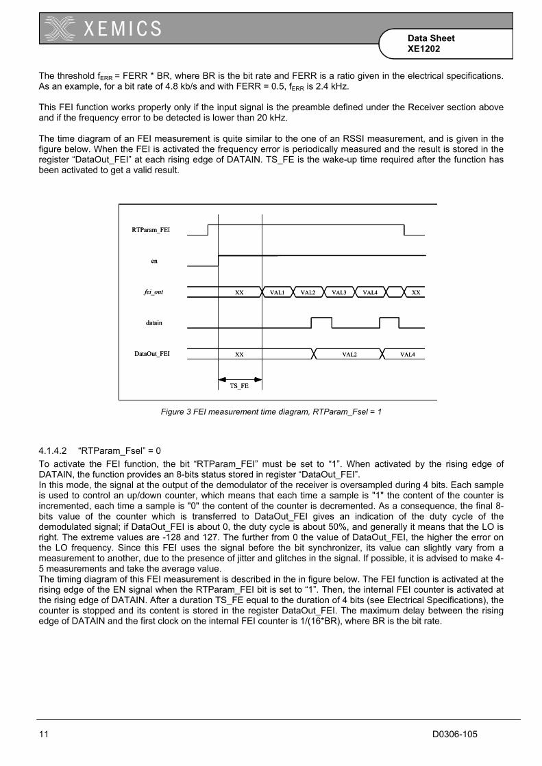
4.1.4 Frequency Error Indicator - FEI When activated, this function provides information about the frequency error of the local oscillator compared with the input carrier frequency. The condition on the modulation index for proper behavior of the FEI function is:
,22 ≥= ∆⋅BRfβ
where ∆f is the frequency deviation and BR is the bit rate. There are 2 modes of operation for this function selected by the bit “RTParam_Fsel” (see the Configuration register section below). IMPORTANT NOTE To guarantee proper behavior of the FEI, the sum of frequency offset and the signal bandwidth (ssb) should be lower than the baseband filter bandwidth (single sided). That is
foffset + SignalBW < Baseband_filterBW
where foffset is the difference between the carrier frequency and the LO frequency, SignalBW is the signal bandwidth (single sided) equal to the sum of the bitrate divided by 2 and the frequency deviation (Bitrate/2 + Frequency Deviation), and Baseband_filterBW is the channel filter bandwidth defined by the RTParam_BW parameter (see the Configuration Registers section below). 4.1.4.1 “RTParam_Fsel” = 1 To activate the FEI function, the bit “RTParam_FEI” must be set to “1”. When activated, the function provides a 2-bits status stored in register “DataOut_FEI”. The meaning of this output is given in the following table, where fLO is the internal local oscillator frequency, and fRF is the carrier frequency of the received signal.
DataOut_FEI Meaning
0 0 fLO-fRF ≤ fERR
0 1 -
1 0 (fLO-fRF) > fERR
1 1 (fLO-fRF) < -fERR
Table 3 FEI status description
XX VAL1 VAL2 VAL3 VAL4 XX
XX VAL2 VAL4
RTParam_RSSI
rssi_out
datain
DataOut_RSSI
TS_RS
en
XX VAL1 VAL2 VAL3 VAL4 XX
XX VAL2 VAL4
RTParam_RSSI
rssi_out
datain
DataOut_RSSI
TS_RS
en
11 D0306-105
Data Sheet XE1202
The threshold fERR = FERR * BR, where BR is the bit rate and FERR is a ratio given in the electrical specifications. As an example, for a bit rate of 4.8 kb/s and with FERR = 0.5, fERR is 2.4 kHz. This FEI function works properly only if the input signal is the preamble defined under the Receiver section above and if the frequency error to be detected is lower than 20 kHz. The time diagram of an FEI measurement is quite similar to the one of an RSSI measurement, and is given in the figure below. When the FEI is activated the frequency error is periodically measured and the result is stored in the register “DataOut_FEI” at each rising edge of DATAIN. TS_FE is the wake-up time required after the function has been activated to get a valid result.
Figure 3 FEI measurement time diagram, RTParam_Fsel = 1
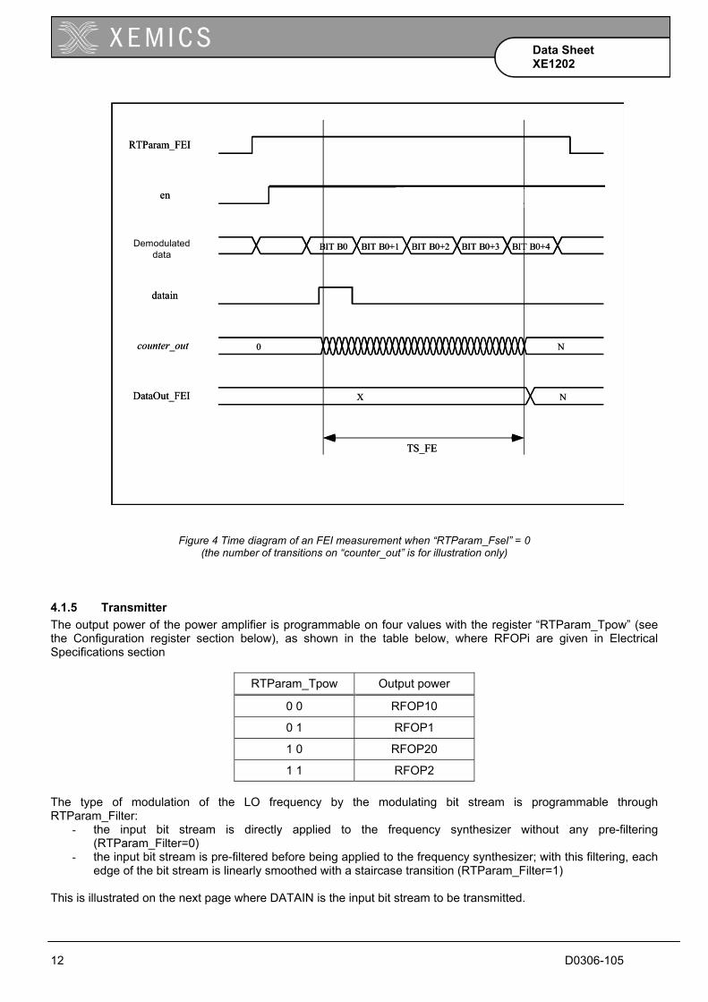
4.1.4.2 “RTParam_Fsel” = 0 To activate the FEI function, the bit “RTParam_FEI” must be set to “1”. When activated by the rising edge of DATAIN, the function provides an 8-bits status stored in register “DataOut_FEI”. In this mode, the signal at the output of the demodulator of the receiver is oversampled during 4 bits. Each sample is used to control an up/down counter, which means that each time a sample is "1" the content of the counter is incremented, each time a sample is "0" the content of the counter is decremented. As a consequence, the final 8-bits value of the counter which is transferred to DataOut_FEI gives an indication of the duty cycle of the demodulated signal; if DataOut_FEI is about 0, the duty cycle is about 50%, and generally it means that the LO is right. The extreme values are -128 and 127. The further from 0 the value of DataOut_FEI, the higher the error on the LO frequency. Since this FEI uses the signal before the bit synchronizer, its value can slightly vary from a measurement to another, due to the presence of jitter and glitches in the signal. If possible, it is advised to make 4-5 measurements and take the average value. The timing diagram of this FEI measurement is described in the in figure below. The FEI function is activated at the rising edge of the EN signal when the RTParam_FEI bit is set to “1”. Then, the internal FEI counter is activated at the rising edge of DATAIN. After a duration TS_FE equal to the duration of 4 bits (see Electrical Specifications), the counter is stopped and its content is stored in the register DataOut_FEI. The maximum delay between the rising edge of DATAIN and the first clock on the internal FEI counter is 1/(16*BR), where BR is the bit rate.
XX VAL1 VAL2 VAL3 VAL4 XX
XX VAL2 VAL4
RTParam_FEI
fei_out
datain
DataOut_FEI
TS_FE
en
XX VAL1 VAL2 VAL3 VAL4 XX
XX VAL2 VAL4
RTParam_FEI
fei_out
datain
DataOut_FEI
TS_FE
en
12 D0306-105
Data Sheet XE1202
Figure 4 Time diagram of an FEI measurement when “RTParam_Fsel” = 0 (the number of transitions on “counter_out” is for illustration only)
4.1.5 Transmitter The output power of the power amplifier is programmable on four values with the register “RTParam_Tpow” (see the Configuration register section below), as shown in the table below, where RFOPi are given in Electrical Specifications section
RTParam_Tpow Output power
0 0 RFOP10
0 1 RFOP1
1 0 RFOP20
1 1 RFOP2 The type of modulation of the LO frequency by the modulating bit stream is programmable through RTParam_Filter:
- the input bit stream is directly applied to the frequency synthesizer without any pre-filtering (RTParam_Filter=0)
- the input bit stream is pre-filtered before being applied to the frequency synthesizer; with this filtering, each edge of the bit stream is linearly smoothed with a staircase transition (RTParam_Filter=1)
This is illustrated on the next page where DATAIN is the input bit stream to be transmitted.
BIT B0 BIT B0+1
X
RTParam_FEI
ffdemod_out
datain
DataOut_FEI
TS_FE
en
BIT B0+2 BIT B0+3 BIT B0+4
0 N
N
counter_out
Demodulateddata
BIT B0 BIT B0+1
X
RTParam_FEI
ffdemod_out
datain
DataOut_FEI
TS_FE
en
BIT B0+2 BIT B0+3 BIT B0+4
0 N
N
counter_out
Demodulateddata

13 D0306-105
Data Sheet XE1202
IN freq_synth
datain
staircase filtering
no filtering
IN freq_synth
trise
tbit
Figure 5 Modulation without and with pre-filtering
The characteristic of the smoothing filter is the ratio trise/tbit. The value of this ratio is programmable with the register “RTParam_Stair”, as shown in the following table.
FSParam_Stair trise/tbit
0 10 %
1 20 %
4.1.6 Pattern recognition XE1202 includes a pattern recognition function. When “ADParam_Pattern” (see the Configuration register section below) is set to “1” this feature is turned on, provided the bit synchronizer is turned on too (the pattern recognition feature doesn’t work if the bit synchronizer is turned off). In this case, the incoming NRZ bit stream is compared with a pattern stored in the “Pattern” register. The length of this pattern can be 8, 16, 24, or 32 bits, as defined by “ADParam_Psize”. When comparing the streams 0, 1, 2, or 3 errors, as defined by “ADParam_Psize” can be allowed to detect a match. The PATTERN output is driven by the output of this comparator. It is “high” when a match is detected, otherwise “low”. When the feature is disabled, the PATTERN output is set to “low”
4.1.7 Frequency synthesizer The exact frequency step of the frequency synthesizer can be obtained from the following equation: FSTEP = FXTAL / 77’824. As an example, if FXTAL is exactly 39 MHz, FSTEP = 501.13 Hz.
14 D0306-105
Data Sheet XE1202
When “RTParam_Clkout” is set high, a frequency divider by 4, 8, 16, or 32, depending on “ADParam_Clkfreq” (see the Configuration register section below), is embedded in XE1202 and provides the CLKOUT clock signal for an MCU or an external circuitry. The input frequency is the 39.0 MHz reference frequency, so the possible clocks available on CLKOUT are 1.22, 2.44, 4.87, or 9.75 MHz. When the XE1202 is in Sleep Mode (MODE[2:0] = 000), this clock is stopped.
5 Interface definition, Principles of operation
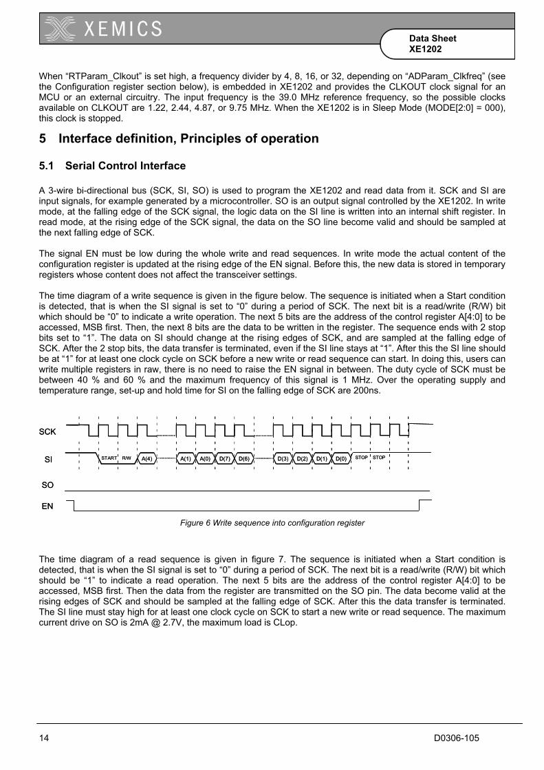
5.1 Serial Control Interface A 3-wire bi-directional bus (SCK, SI, SO) is used to program the XE1202 and read data from it. SCK and SI are input signals, for example generated by a microcontroller. SO is an output signal controlled by the XE1202. In write mode, at the falling edge of the SCK signal, the logic data on the SI line is written into an internal shift register. In read mode, at the rising edge of the SCK signal, the data on the SO line become valid and should be sampled at the next falling edge of SCK. The signal EN must be low during the whole write and read sequences. In write mode the actual content of the configuration register is updated at the rising edge of the EN signal. Before this, the new data is stored in temporary registers whose content does not affect the transceiver settings. The time diagram of a write sequence is given in the figure below. The sequence is initiated when a Start condition is detected, that is when the SI signal is set to “0” during a period of SCK. The next bit is a read/write (R/W) bit which should be “0” to indicate a write operation. The next 5 bits are the address of the control register A[4:0] to be accessed, MSB first. Then, the next 8 bits are the data to be written in the register. The sequence ends with 2 stop bits set to “1”. The data on SI should change at the rising edges of SCK, and are sampled at the falling edge of SCK. After the 2 stop bits, the data transfer is terminated, even if the SI line stays at “1”. After this the SI line should be at “1” for at least one clock cycle on SCK before a new write or read sequence can start. In doing this, users can write multiple registers in raw, there is no need to raise the EN signal in between. The duty cycle of SCK must be between 40 % and 60 % and the maximum frequency of this signal is 1 MHz. Over the operating supply and temperature range, set-up and hold time for SI on the falling edge of SCK are 200ns.
START R/W A(4) A(1) A(0) D(7) D(6) D(3) D(2) D(1) D(0)SI
SCK
SO
STOP STOP
EN
START R/W A(4) A(1) A(0) D(7) D(6) D(3) D(2) D(1) D(0)SI
SCK
SO
STOP STOP
EN Figure 6 Write sequence into configuration register
The time diagram of a read sequence is given in figure 7. The sequence is initiated when a Start condition is detected, that is when the SI signal is set to “0” during a period of SCK. The next bit is a read/write (R/W) bit which should be “1” to indicate a read operation. The next 5 bits are the address of the control register A[4:0] to be accessed, MSB first. Then the data from the register are transmitted on the SO pin. The data become valid at the rising edges of SCK and should be sampled at the falling edge of SCK. After this the data transfer is terminated. The SI line must stay high for at least one clock cycle on SCK to start a new write or read sequence. The maximum current drive on SO is 2mA @ 2.7V, the maximum load is CLop.

15 D0306-105
Data Sheet XE1202
START R/W A(4) A(0)SI
SCK
SO D(7) D(6) D(5) D(4) D(3) D(2) D(1) D(0)
EN
START R/W A(4) A(0)SI
SCK
SO D(7) D(6) D(5) D(4) D(3) D(2) D(1) D(0)
EN Figure 7 Read sequence into configuration register
When the serial interface is not used for read or write operations, both SCK and SI should be set to “1”. Except in read mode, SO is set to “0”.
5.2 Configuration and Status registers XE1202 has a series of configuration registers programmable through the serial control interface described above. Their name, size, address and description are listed in the table below. The size of these registers is 1, 2, 3, or 4 bytes. Their byte address is 5 bit address, A[4:0]. In addition, there is one register, DataOut, from which users can read various transceiver status information.
Name Size Byte Address Description
RTParam 2 x 8 bit 00000 00001
Receiver and transmitter parameters registers
FSParam 3 x 8 bit 00010 00011 00100
Frequency parameters
DataOut 1 x 8 bit 00101 Transceiver data register
ADParam 2 x 8 bit 00110 00 111
Additional parameters
Pattern 4 x 8 bit 01000 01001 01010 01011
Reference pattern for the “pattern recognition” function
In addition, 16 bytes at addresses A[4:0] = 10000 to 11111 are reserved for test purpose
Name Size Byte Address Description
Test 16 x 8 bit 10000 to 11111 Test registers (reserved) All the bits that are referred as “reserved” in this section should be set to “0”.
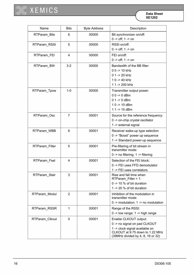
5.2.1 RTParam configuration register
Name Bits Byte Address Description
RTParam_Rmode 7 00000 Receiver modes: 0 -> A-mode (high sensitivity) 1 -> B-mode (high linearity)
16 D0306-105
Data Sheet XE1202
Name Bits Byte Address Description
RTParam_Bits 6 00000 Bit synchronizer on/off: 0 -> off; 1 -> on
RTParam_RSSI 5 00000 RSSI on/off: 0 -> off; 1 -> on
RTParam_FEI 4 00000 FEI on/off: 0 -> off; 1 -> on
RTParam_BW 3-2 00000 Bandwidth of the BB filter: 0 0 -> 10 kHz 0 1 -> 20 kHz 1 0 -> 40 kHz 1 1 -> 200 kHz
RTParam_Tpow 1-0 00000 Transmitter output power: 0 0 -> 0 dBm 0 1 -> 5 dBm 1 0 -> 10 dBm 1 1 -> 15 dBm
RTParam_Osc 7 00001 Source for the reference frequency: 0 -> on-chip crystal oscillator 1 -> external signal
RTParam_WBB 6 00001 Receiver wake-up type selection 0 -> “Boost” power up sequence 1 -> Standard power-up sequence
RTParam_Filter 5 00001 Pre-filtering of bit stream in transmitter mode: 0 -> no filtering; 1 -> filtering
RTParam_Fsel 4 00001 Selection of the FEI block: 0 -> FEI uses FFD demodulator 1 -> FEI uses correlators
RTParam_Stair 3 00001 Rise and fall time when RTParam_Filter = 1: 0 -> 10 % of bit duration 1 -> 20 % of bit duration
RTParam_Modul 2 00001 Inhibition of the modulation in transmitter mode: 0 -> modulation; 1 -> no modulation
RTParam_RSSR 1 00001 Range of the RSSI: 0 -> low range; 1 -> high range
RTParam_Clkout 0 00001 Enable CLKOUT output: 0 -> no signal on pad CLKOUT 1 -> clock signal available on CLKOUT at 9.75 down to 1.22 MHz (39MHz divided by 4, 8, 16 or 32)
17 D0306-105
Data Sheet XE1202
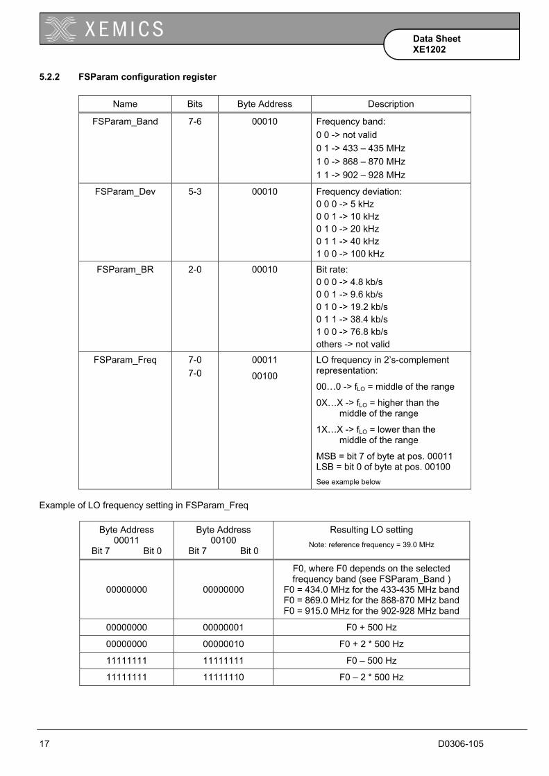
5.2.2 FSParam configuration register
Name Bits Byte Address Description
FSParam_Band 7-6 00010 Frequency band: 0 0 -> not valid 0 1 -> 433 – 435 MHz 1 0 -> 868 – 870 MHz 1 1 -> 902 – 928 MHz
FSParam_Dev 5-3 00010 Frequency deviation: 0 0 0 -> 5 kHz 0 0 1 -> 10 kHz 0 1 0 -> 20 kHz 0 1 1 -> 40 kHz 1 0 0 -> 100 kHz
FSParam_BR 2-0 00010 Bit rate: 0 0 0 -> 4.8 kb/s 0 0 1 -> 9.6 kb/s 0 1 0 -> 19.2 kb/s 0 1 1 -> 38.4 kb/s 1 0 0 -> 76.8 kb/s others -> not valid
FSParam_Freq 7-0 7-0
00011
00100
LO frequency in 2’s-complement representation:
00…0 -> fLO = middle of the range
0X…X -> fLO = higher than the middle of the range
1X…X -> fLO = lower than the middle of the range
MSB = bit 7 of byte at pos. 00011 LSB = bit 0 of byte at pos. 00100 See example below
Example of LO frequency setting in FSParam_Freq
Byte Address 00011
Bit 7 Bit 0
Byte Address 00100
Bit 7 Bit 0
Resulting LO setting Note: reference frequency = 39.0 MHz
00000000
00000000
F0, where F0 depends on the selected frequency band (see FSParam_Band )
F0 = 434.0 MHz for the 433-435 MHz band F0 = 869.0 MHz for the 868-870 MHz band F0 = 915.0 MHz for the 902-928 MHz band
00000000 00000001 F0 + 500 Hz
00000000 00000010 F0 + 2 * 500 Hz
11111111 11111111 F0 – 500 Hz
11111111 11111110 F0 – 2 * 500 Hz

18 D0306-105
Data Sheet XE1202
5.2.3 DataOut register
Name Bits Byte Address Description
DataOut_RSSI 7-6 00101 RSSI output: 0 0 -> lowest level 0 1 -> 2nd level 1 0 -> 3rd level 1 1 -> highest level
DataOut_FEI When
RTParam_Fsel = 0
7-0 00101 FEI output: Output of the up/down counter in 2’s-complement representation MSB = bit 7
DataOut_FEI When
RTParam_Fsel = 1
5-4 00101 FEI output: 0 0 -> frequency OK 1 0 -> frequency too low 1 1 -> frequency too high
5.2.4 ADParam configuration register
Name Bits Byte Address Description
ADParam_Pattern 7 00110 Pattern recognition on/off: 0 -> off 1 -> on
ADParam_Psize 6-5 00110 Size of the reference for pattern recognition: 0 0 -> 8 bits 0 1 -> 16 bits 1 0 -> 24 bits 1 1 -> 32 bits
ADParam_Ptol 4-3 00110 Number of tolerated errors for the pattern recognition: 0 0 -> 0 error 0 1 -> 1 error 1 0 -> 2 errors 1 1 -> 3 errors
ADParam_Clkfreq 2-1 00110 Frequency on CLKOUT: 0 0 -> 1.22 MHz (div. ratio: 32) 0 1 -> 2.44 MHz (div. ratio: 16) 1 0 -> 4.87 MHz (div. ratio: 8) 1 1 -> 9.75 MHz (div. ratio: 4)
ADParam_IQA 0 00110 IQ amplifiers on/off: 0 -> off 1 -> on
ADParam_Res1 7 00111 Reserved. Should be set to “0”
ADParam_Invert 6 00111 Inversion of the output data of the receiver: 0 -> non-inverted data 1 -> inverted data
19 D0306-105
Data Sheet XE1202
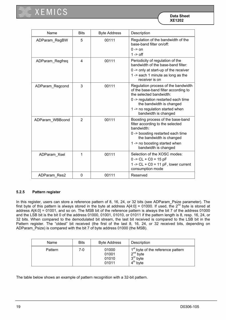
Name Bits Byte Address Description
ADParam_RegBW 5 00111 Regulation of the bandwidth of the base-band filter on/off: 0 -> on 1 -> off
ADParam_Regfreq 4 00111 Periodicity of regulation of the bandwidth of the base-band filter: 0 -> only at start-up of the receiver 1 -> each 1 minute as long as the receiver is on
ADParam_Regcond 3 00111 Regulation process of the bandwidth of the base-band filter according to the selected bandwidth: 0 -> regulation restarted each time the bandwidth is changed 1 -> no regulation started when bandwidth is changed
ADParam_WBBcond 2 00111 Boosting process of the base-band filter according to the selected bandwidth: 0 -> boosting restarted each time the bandwidth is changed 1 -> no boosting started when bandwidth is changed
ADParam_Xsel 1 00111 Selection of the XOSC modes: 0 -> CL + C0 = 15 pF 1 -> CL + C0 = 11 pF, lower current consumption mode
ADParam_Res2 0 00111 Reserved
5.2.5 Pattern register In this register, users can store a reference pattern of 8, 16, 24, or 32 bits (see ADParam_Psize parameter). The first byte of this pattern is always stored in the byte at address A[4:0] = 01000. If used, the 2nd byte is stored at address A[4:0] = 01001, and so on. The MSB bit of the reference pattern is always the bit 7 of the address 01000 and the LSB bit is the bit 0 of the address 01000, 01001, 01010, or 01011 if the pattern length is 8, resp. 16, 24, or 32 bits. When compared to the demodulated bit stream, the last bit received is compared to the LSB bit in the Pattern register. The “oldest” bit received (the first of the last 8, 16, 24, or 32 received bits, depending on ADParam_Psize) is compared with the bit 7 of byte address 01000 (the MSB).
Name Bits Byte Address Description
Pattern 7-0 01000 01001 01010 01011
1st byte of the reference pattern 2nd byte 3rd byte 4th byte
The table below shows an example of pattern recognition with a 32-bit pattern.
20 D0306-105
Data Sheet XE1202
Byte Address 01000
Bit 7 Bit 0
Byte Address 01001
Bit 7 Bit 0
Byte Address 01010
Bit 7 Bit 0
Byte Address 01011
Bit 7 Bit 0
10010011 10101010 10010011 10101010
101 10010011 10101010 10010011 10101010
previous bits from
demodulator
last bit received
The table below shows an example of pattern recognition with an 8-bit pattern.
Byte Address 01000
Bit 7 Bit 0
Byte Address 01001
Bit 7 Bit 0
Byte Address 01010
Bit 7 Bit 0
Byte Address 01011
Bit 7 Bit 0
10010011 xxxxxxxx xxxxxxxx xxxxxxxx
101 10010011
previous bits from
demodulator
last bit received
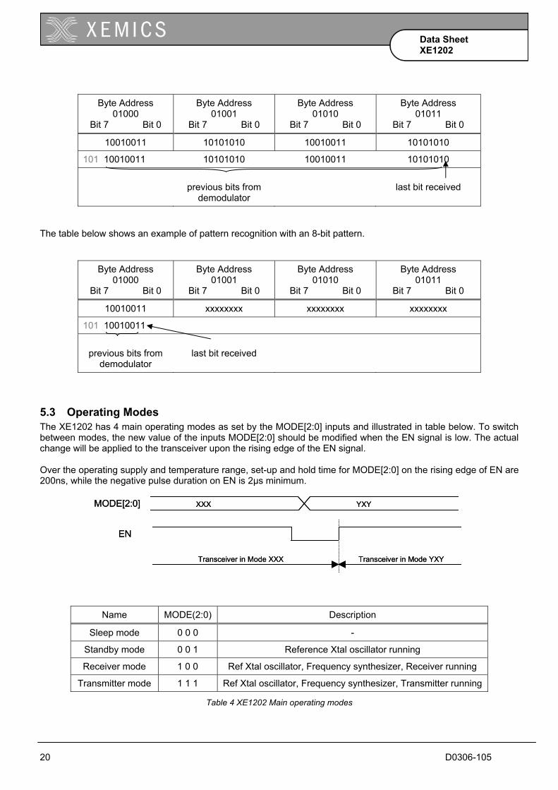
5.3 Operating Modes The XE1202 has 4 main operating modes as set by the MODE[2:0] inputs and illustrated in table below. To switch between modes, the new value of the inputs MODE[2:0] should be modified when the EN signal is low. The actual change will be applied to the transceiver upon the rising edge of the EN signal. Over the operating supply and temperature range, set-up and hold time for MODE[2:0] on the rising edge of EN are 200ns, while the negative pulse duration on EN is 2µs minimum.
Name MODE(2:0) Description
Sleep mode 0 0 0 -
Standby mode 0 0 1 Reference Xtal oscillator running
Receiver mode 1 0 0 Ref Xtal oscillator, Frequency synthesizer, Receiver running
Transmitter mode 1 1 1 Ref Xtal oscillator, Frequency synthesizer, Transmitter running
Table 4 XE1202 Main operating modes
XXXMODE[2:0]
EN
YXY
Transceiver in Mode XXX Transceiver in Mode YXY
XXXMODE[2:0]
EN
YXY
Transceiver in Mode XXX Transceiver in Mode YXY
21 D0306-105
Data Sheet XE1202
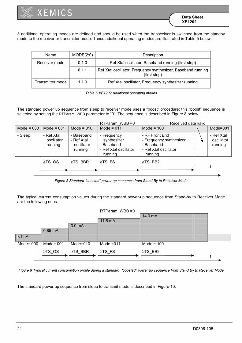
3 additional operating modes are defined and should be used when the transceiver is switched from the standby mode to the receiver or transmitter mode. These additional operating modes are illustrated in Table 5 below.
Name MODE(2:0) Description
0 1 0 Ref Xtal oscillator, Baseband running (first step) Receiver mode
0 1 1 Ref Xtal oscillator, Frequency synthesizer, Baseband running (first step)
Transmitter mode 1 1 0 Ref Xtal oscillator, Frequency synthesizer running
Table 5 XE1202 Additional operating modes
The standard power up sequence from sleep to receiver mode uses a “boost” procedure; this “boost” sequence is selected by setting the RTParam_WBB parameter to “0”. The sequence is described in Figure 8 below. RTParam_WBB =0 Received data valid Mode = 000 Mode = 001 Mode = 010 Mode = 011 Mode = 100 Mode=001
- Sleep - Ref Xtal oscillator running
- Baseband - Ref Xtal
oscillator running
- Frequency synthesizer
- Baseband - Ref Xtal oscillator
running
- RF Front End - Frequency synthesizer - Baseband - Ref Xtal oscillator
running
- Ref Xtal oscillator running
≥TS_OS ≥TS_BBR ≥TS_FS ≥TS_BB2
t
Figure 8 Standard “boosted” power up sequence from Stand By to Receiver Mode
The typical current consumption values during the standard power-up sequence from Stand-by to Receiver Mode are the following ones. RTParam_WBB =0 14.0 mA 11.5 mA 3.0 mA 0.85 mA <1 uA
Mode= 000 Mode= 001 Mode=010 Mode =011 Mode = 100
≥TS_OS ≥TS_BBR ≥TS_FS ≥TS_BB2
t
Figure 9 Typical current consumption profile during a standard “boosted” power up sequence from Stand By to Receiver Mode
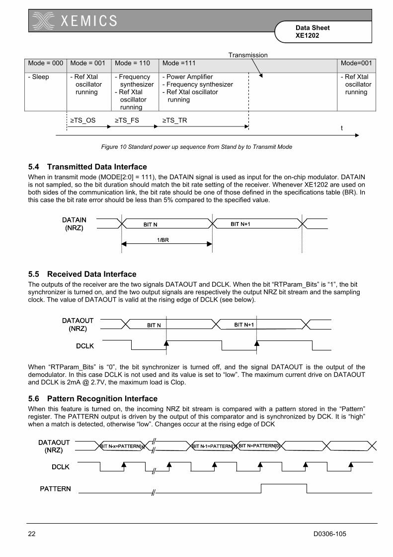
The standard power up sequence from sleep to transmit mode is described in Figure 10.
22 D0306-105
Data Sheet XE1202
Transmission Mode = 000 Mode = 001 Mode = 110 Mode =111 Mode=001
- Sleep - Ref Xtal oscillator running
- Frequency synthesizer
- Ref Xtal oscillator running
- Power Amplifier - Frequency synthesizer - Ref Xtal oscillator
running
- Ref Xtal oscillator running
≥TS_OS ≥TS_FS ≥TS_TR t
Figure 10 Standard power up sequence from Stand by to Transmit Mode
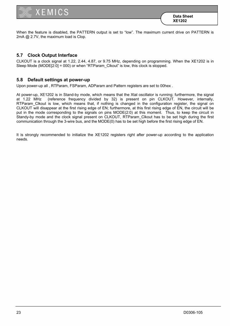
5.4 Transmitted Data Interface When in transmit mode (MODE[2:0] = 111), the DATAIN signal is used as input for the on-chip modulator. DATAIN is not sampled, so the bit duration should match the bit rate setting of the receiver. Whenever XE1202 are used on both sides of the communication link, the bit rate should be one of those defined in the specifications table (BR). In this case the bit rate error should be less than 5% compared to the specified value.
5.5 Received Data Interface The outputs of the receiver are the two signals DATAOUT and DCLK. When the bit “RTParam_Bits” is “1”, the bit synchronizer is turned on, and the two output signals are respectively the output NRZ bit stream and the sampling clock. The value of DATAOUT is valid at the rising edge of DCLK (see below).
When “RTParam_Bits” is “0”, the bit synchronizer is turned off, and the signal DATAOUT is the output of the demodulator. In this case DCLK is not used and its value is set to “low”. The maximum current drive on DATAOUT and DCLK is 2mA @ 2.7V, the maximum load is Clop.
5.6 Pattern Recognition Interface When this feature is turned on, the incoming NRZ bit stream is compared with a pattern stored in the “Pattern” register. The PATTERN output is driven by the output of this comparator and is synchronized by DCK. It is “high” when a match is detected, otherwise “low”. Changes occur at the rising edge of DCK
DATAIN(NRZ) BIT N BIT N+1
1/BR
DATAIN(NRZ) BIT N BIT N+1
1/BR
DATAOUT(NRZ)
DCLK
BIT N BIT N+1DATAOUT
(NRZ)
DCLK
BIT N BIT N+1
DATAOUT(NRZ)
DCLK
BIT N=PATTERN[0]
PATTERN
BIT N-1=PATTERN[1]BIT N-x=PATTERN[x]DATAOUT(NRZ)
DCLK
BIT N=PATTERN[0]
PATTERN
BIT N-1=PATTERN[1]BIT N-x=PATTERN[x]
23 D0306-105
Data Sheet XE1202
When the feature is disabled, the PATTERN output is set to “low”. The maximum current drive on PATTERN is 2mA @ 2.7V, the maximum load is Clop.
5.7 Clock Output Interface CLKOUT is a clock signal at 1.22, 2.44, 4.87, or 9.75 MHz, depending on programming. When the XE1202 is in Sleep Mode (MODE[2:0] = 000) or when “RTParam_Clkout” is low, this clock is stopped.
5.8 Default settings at power-up Upon power-up all , RTParam, FSParam, ADParam and Pattern registers are set to 00hex . At power-up, XE1202 is in Stand-by mode, which means that the Xtal oscillator is running; furthermore, the signal at 1.22 MHz (reference frequency divided by 32) is present on pin CLKOUT. However, internally, RTParam_Clkout is low, which means that, if nothing is changed in the configuration register, the signal on CLKOUT will disappear at the first rising edge of EN; furthermore, at this first rising edge of EN, the circuit will be put in the mode corresponding to the signals on pins MODE(2:0) at this moment. Thus, to keep the circuit in Standy-by mode and the clock signal present on CLKOUT, RTParam_Clkout has to be set high during the first communication through the 3-wire bus, and the MODE(0) has to be set high before the first rising edge of EN. It is strongly recommended to initialize the XE1202 registers right after power-up according to the application needs.
24 D0306-105
Data Sheet XE1202
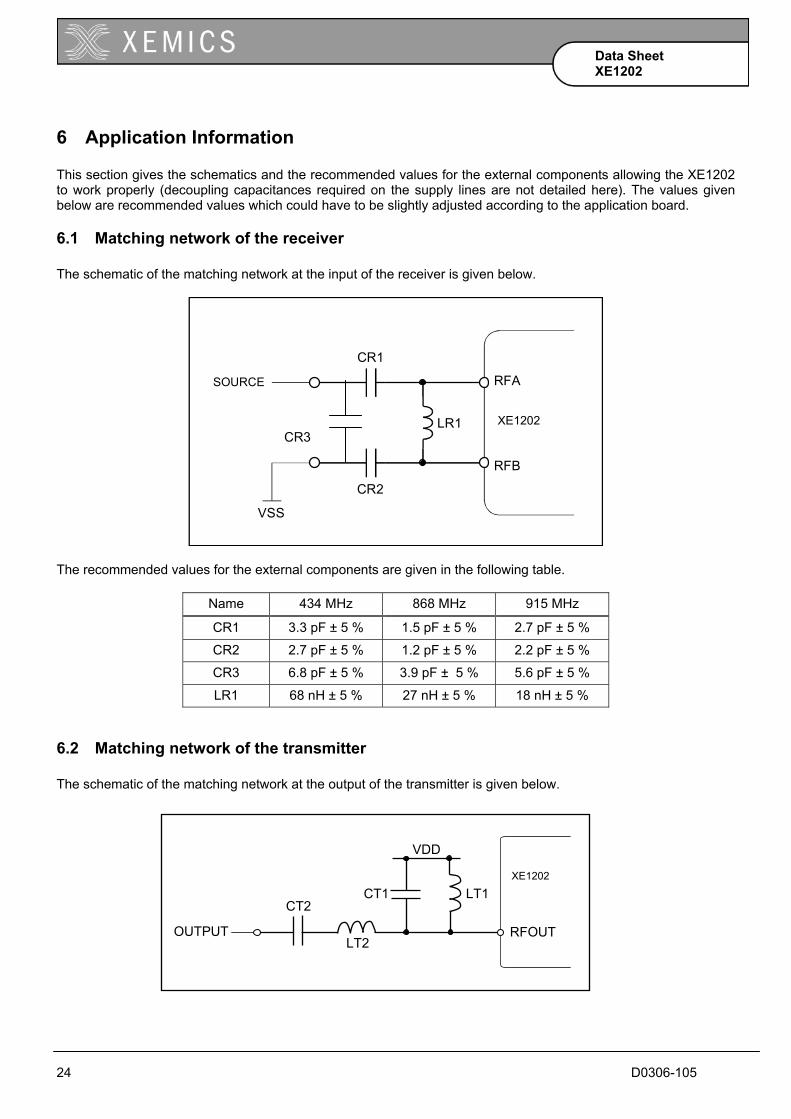
6 Application Information This section gives the schematics and the recommended values for the external components allowing the XE1202 to work properly (decoupling capacitances required on the supply lines are not detailed here). The values given below are recommended values which could have to be slightly adjusted according to the application board.
6.1 Matching network of the receiver The schematic of the matching network at the input of the receiver is given below.
CR1
CR2
LR1
RFA
RFB
SOURCE
EAGLE ASIC
VSS
The recommended values for the external components are given in the following table.
Name 434 MHz 868 MHz 915 MHz
CR1 3.3 pF ± 5 % 1.5 pF ± 5 % 2.7 pF ± 5 % CR2 2.7 pF ± 5 % 1.2 pF ± 5 % 2.2 pF ± 5 % CR3 6.8 pF ± 5 % 3.9 pF ± 5 % 5.6 pF ± 5 % LR1 68 nH ± 5 % 27 nH ± 5 % 18 nH ± 5 %
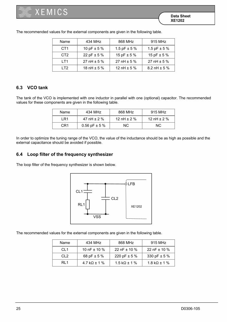
6.2 Matching network of the transmitter The schematic of the matching network at the output of the transmitter is given below.
OUTPUT RFOUT
CT1 CT2
LT2
LT1 XE1202
VDD
CR3
XE1202
25 D0306-105
Data Sheet XE1202
The recommended values for the external components are given in the following table.
Name 434 MHz 868 MHz 915 MHz
CT1 10 pF ± 5 % 1.5 pF ± 5 % 1.5 pF ± 5 % CT2 22 pF ± 5 % 15 pF ± 5 % 15 pF ± 5 % LT1 27 nH ± 5 % 27 nH ± 5 % 27 nH ± 5 % LT2 18 nH ± 5 % 12 nH ± 5 % 8.2 nH ± 5 %
6.3 VCO tank The tank of the VCO is implemented with one inductor in parallel with one (optional) capacitor. The recommended values for these components are given in the following table.
Name 434 MHz 868 MHz 915 MHz
LR1 47 nH ± 2 % 12 nH ± 2 % 12 nH ± 2 % CR1 0.56 pF ± 5 % NC NC
In order to optimize the tuning range of the VCO, the value of the inductance should be as high as possible and the external capacitance should be avoided if possible.
6.4 Loop filter of the frequency synthesizer The loop filter of the frequency synthesizer is shown below.
The recommended values for the external components are given in the following table.
Name 434 MHz 868 MHz 915 MHz
CL1 10 nF ± 10 % 22 nF ± 10 % 22 nF ± 10 % CL2 68 pF ± 5 % 220 pF ± 5 % 330 pF ± 5 % RL1 4.7 kΩ ± 1 % 1.5 kΩ ± 1 % 1.8 kΩ ± 1 %
LFB
CL2 RL1 XE1202
VSS
CL1
26 D0306-105
Data Sheet XE1202
6.5 Reference crystal for the frequency synthesizer For narrow band applications, where users select the lowest frequency deviation and the narrowest baseband filter, the crystal for reference oscillator of the frequency synthesizer must have the following characteristics:
Name Description Min. value Typ. value Max. value Fs Nominal frequency - 39.0 MHz
(fundamental) -
CL Load capacitance for fs (on-chip) - 8 pF (*) - Rm Motional resistance - - 40 Ω Cm Motional capacitance - - 30 fF C0 Shunt capacitance - - 7 pF (*) ∆fs(0) Calibration tolerance at 25 °C - - 10 ppm ∆fs(∆T) Stability over temperature range
(-40 °C to 85 °C) - - 10 ppm
∆fs(∆t) Aging tolerance in first 5 years - - 5 ppm Table 6 Crystal characteristics
(*) The on-chip oscillator is implemented in two selectable versions: the first for CL = 8 pF and C0 = 7 pF, and the second for CL = 8 pF and C0 = 3 pF; the latter will allow a higher amplitude for the internal signal with a slightly lower consumption. The electrical specifications given in section 3.2.2 are valid provided the crystal satisfies the specifications given in table 5. For less demanding applications in term of signal bandwidth and/or temperature range, it is possible to use crystal with larger values for ∆fs(0), ∆fs(∆T), and/or ∆fs(∆t). In this case foffset + BWssb should be lower than BWfilter, where foffset is the offset (error) on the carrier frequency (the sum of ∆fs(0), ∆fs(∆T), and/or ∆fs(∆t)), BWssb is the single side-band bandwidth of the signal, and BWfilter is the single side-band bandwidth of the base-band filter. XE1202 can be used with reference crystal operating on its 3rd harmonic at 39.00 MHz. This has 2 consequences: a) the oscillator start-up time is higher than in fundamental mode; and b) an extra 1.5k to 16k ohm external resistor has to be placed in parallel to the crystal. In this case, the crystal should have Cload = 8 to 10pF, Rm < 60 ohm, C0 < 7pF.
27 D0306-105
Data Sheet XE1202
7 Packaging information XE1202 comes in 44-lead LQFP package
XEMICS 2003 All rights reserved. Reproduction in whole or in part is prohibited without the prior written consent of the copyright owner. The information presented in this document does not form part of any quotation or contract, is believed to be accurate and reliable and may be changed without notice. No liability will be accepted by the publisher for any consequence of its use. Publication thereof does not convey nor imply any license under patent or other industrial or intellectual property rights. XEMICS PRODUCTS ARE NOT DESIGNED, INTENDED, AUTHORIZED OR WARRANTED TO BE SUITABLE FOR USE IN LIFE-SUPPORT APPLICATIONS, DEVICES OR SYSTEMS OR OTHER CRITICAL APPLICATIONS. INCLUSION OF XEMICS PRODUCTS IN SUCH APPLICATIONS IS UNDERSTOOD TO BE UNDERTAKEN SOLELY AT THE CUSTOMER’S OWN RISK. Should a customer purchase or use XEMICS products for any such unauthorized application, the customer shall indemnify and hold XEMICS and its officers, employees, subsidiaries, affiliates, and distributors harmless against all claims, costs damages and attorney fees which could arise.
IAMP
QAMP
VDDA
XTB
VSSA
XTA
VSS
VSSA
MODE(1)
MODE(0)
ENVSSF
RFA
RFB
VSSP
RFOUT
VDDP
TVCO
MO
DE(
2)
DA
TAIN
DA
TAO
UT
DC
LK
VD
D
SCK
SO
SI
VDD
F
TKA
TKB
VSS
F
LFB
VD
DD
TSU
PP
VSS
VSS
D
VSSP
VSS
VSS
VSS CLK
OU
T
VSS
SCAN VS
S
PATT
ERN
IAMP
QAMP
VDDA
XTB
VSSA
XTA
VSS
VSSA
MODE(1)
MODE(0)
ENVSSF
RFA
RFB
VSSP
RFOUT
VDDP
TVCO
MO
DE(
2)
DA
TAIN
DA
TAO
UT
DC
LK
VD
D
SCK
SO
SI
VDD
F
TKA
TKB
VSS
F
LFB
VD
DD
TSU
PP
VSS
VSS
D
VSSP
VSS
VSS
VSS CLK
OU
T
VSS
SCAN VS
S
PATT
ERN