Embed Size (px)
Citation preview

Order this document by MC1495/DI
MOTOROLA
Wideband LinearFour=Quadrant Multiplier
The MC1 495 is designed for use where the output is a linear product oftwo input voltages. Maximum versatility is assured by allowing the user toselect the level shift method. Typical applications include: multiply, divide*,square root*, mean square*, phase detector, frequency doubler, balancedmodulator/demodulator, and electronic gain control.
●
●
●
●
●
●
MCI 495
I I
Excellent Linearity:
27. max Error on X Input, 47. max Error on Y Input Over Temperature@”1YOmax Error on X Input, 2Y. max Error on Y Input at + 25°C ‘
.J*::,!:,\’t~+$,
Adjustable Scale Factor, K.’, +:*}
,>.:\:*.‘ ‘‘i’$i},
Excellent Temperature Stability ,is(i:+>,. ,‘.*.,..;$ .,:,.
Wide Input Voltage Range: t 10 V;,..+\ *~;\m,,3r&\.+.:~.f>.,s,,,.$;,.
+15 V Operation..,}+:,:,,!<,.,,.+,.,
~:\.,:,\
INGS (TA = + 25°C, unless othewise noted.)
Symbol Value Unit
AV 30 Vdc1, V1-vg, V1-V,2, V,-V4,
~“’~l-va,V12-V7, vg-v7, V8-V7, V4-V7)
Differential Input Signal v12–vg f (6+113 Rx) Vdcv4–v8 * (6+13 Ry)
I D SUFFIXPLASTIC PACKAGE
CASE 751A(s0-14)
1
1
P SUFFIXPLASTIC PACKAGE
CASE 646
ORDERING INFORMATIONMaximum Bias Current 13 10 mA
113 10Tested Opereting
Device Temperature Range PackageOperating Temperature Range TA ‘c
MC1 495 0 to +70MC1495D so-1 4
TA = 0° to + 70°CMC1495B – 40 tO +125 MC1495P Plastic DIP
Storage Temperature Range Tstg –65to +150 Oc MC1495BP TA = – 40° to +125°C Plastic DIP
0 Motorola, inc. 1995

MC1495
ELECTRICAL CHARACTERISTICS (+V = + 32 V, -V = -15 V, TA = + 25°C, 13= 113= 1.0 mA, RX = Ry = 15 kQ, RL = 11 kQ, unlessothe~ise noted.)
.
Characteristics Figure Symbol Min Typ Max Unit
-ineaflty (Output Error in percent of full scale) 5 0/0
TA = + 25°C-lo<vx<+lo (vy=*lov) ERX - tl .0 *1.0-lo<vy<+lo (vx=*lov) ,. ERy - * 2.0 * 2.0
TA = TLOWtO THigh-locvx<+lo (vy=flov) ERX - *1.5 t 2.0-Io<vy< +lo(vx=tlov) ERy -
,+!$* 3.0 f 4.0 ..:<!+
:s:~+:>:.,.,
SquareMode Error (Accuracy in percent of full scale after 5 ESQ ,y’;;&>a:
Offset and scale Factor adjustment).:., js
TA = + 25°C‘~::j~#,,,~.>,~,,.~~:~$
* 0.75S>,‘~’— —,,??.:\.‘~:f;,,,
TA = TLOWtOTHigh *1,0 ;?;..,:i$$“+$— ,~r ~:.-~..,:!
Scale Factor (Adjustable)
(
2RL
)
— K 0.1,:~~,,.:* ‘ .—
K=..*,*,‘~$~.>$:s’
13 RxRy.,...’,.>*+>\,,*
,:’.:..,, S$..,~:.k,~}~, \,~
Input Resistance (f= 20 Hz) 7‘.,., .
RinX - 3@*k\;~., – MfiRiny – ~’*&$ ““ -
DifferentialOutput Resistance (f= 20 Hz) 8 RO – ,;;>$~p - kQ
Input Bias Current *’rj*i,i,.,<.,,6\%.,:s+,!, ‘~‘\ . PA
,bx =(lg + 112) (14+ 18) TA = + 25°C Ibx, Iby,~
~, ~~ 2.0 8.0..3:...— l~y=y
2’TA = TLOWtOTHigh .*$,.gcvq,.
.,,. 2.0 12{.,!~,)),,,.~j.. ‘::J$,~ .,,.
Input Offset Current
,,.,,?>
6.,,:”,,*, ....
~..,,,~,:.,+:~;$$.”llg-1121
pATA = + 25°C Il\Qxll?$;l -
114-1810.4 1.0
TA = TLOWtOTHigh ,13:;!,, —,.,., 0.4 2.0
Average Temperature Coefficient of Input Offset Current 6 ~f*:‘+$%I?*[iOlTA = TLOWto THigh
nNOC?: —.~.~‘*y<,,\:j.. 2.5 —
Output Offset Current TA = + 25°C e~’~~ ‘“’ 11001 10 501114-121
PATA = TLOWto THigh > “?* — 20 100
Average Temperature Coefficient of Output Offset Current ~i/.:,..,
6 lTCIOOlTA = TLOWtOTHigh
.).‘\\&*,\nN”C
,, 20,.,:,~!.+ .?,.Frequency Response \N~>~\+l,,;‘*/.,!..,.},$3........*.::1~ 9,10
3.0 dB Bandwidth, RL = 11 kQ,,}..”t., ,.< “..,.~ BW(3dB) - 3.0 MHz.s:>,,...,
3.0 dB Bandwidth, RL = 50 Q (Transconductan@,@~@ dth)—
TBW(3dB) - 803° Relative Phase Shift Between VX and VyWJ:Y@,.+
—.,.,\ “~:.+?;\J.,,‘‘~
MHzfq – 750 kHz
1YeAbsolute Error Due to Input-Output Ph~~i~~~—
fe — 30 — kHz
Common Mode Input Swingsty~ ,?
.s$,.’* *~\*. 11.~:~ ,,$ CMV(Either Input)
Vdct:,~,
.,,. ~t), ;? *1 0.5 *12 —
Common Mode Gain ~~:’ ~’:+~..+. TA = + 25°C 11
(Either Input) ~a,~~$$~~ TA = TLOWto THighACM – 50 -60 — dB
– 40 -50 —
Common Mode Quiescent i’r$~$f$ 12.(.\” Vol - 21Output Voltage
— Vdc~,;;.Y;si~$ ~ V02 - 21 —
Differential Output,~o$~&~wing Capability 9 Vo –, ,., +14 — vpk
power SUPPIY*~%ti& 12 s+ _ 5.0.Jj:>ji. .::,
— mVN,,,,, .<>,\ s- - 10 —
Power S*pl~&urrent 12 17 6.0 7.0 mA,,‘b,.,.t..DC@m;Dssipation 12 pD - 135 170 mW,J>.k,,,,\ .....
~wt. THigh= +70°CfOr MC1495 TLOW= O°Cfor MC1495‘$; =+1 25°C for MCI 495B =- 40°C for MC1495B
2 MOTOROLA ANALOG IC DEVICE DATA

●
MC1495
Figure 1. Multiplier Transfer Characteristic Figure 2. Transconductance Bandwidth
-8.0–in
Y Input
214
9
12
1110
Output (KXY)
X Input
. .. >-.. .- <
‘#l* 10k
~
Onset
I i4—
5.0 k AdjustScale — v.Factor A 1Adjust
y__ $0.tpF -
●
-15 v—
NOTE: Adjust “Scale Factor AdjuaV for a null in VE.ThiS schematic forillustrative purposes only, not specified for test condtions.
MOTOROLA ANALOG [C DEVICE DATA 3

MC1 495
Figure 5. Linearity (Using X-Y Plotter Technique)
Ry=15k Rx=15k t32v
** Tm
Figure 9. Bandwidth (RL = 11 kQ)
Ry=15k Rx=15k t32v●
4ein= 1.0V~S 1 9.1k
q“ 2 llk
—=
ScaleFactor
4 MOTOROLA ANALOG IC DEVICE DATA

MCI 495
Figure 10. Bandwidth (RL = 50 Q)
o Ry=510 Rx=510 t15v
4q“ = 1.0 Vms l.Ok
)
, 2 50)
MC1495 ;50
— 13
— — 3( 7R13
I
— 0,1 pF
K=40 12k13,7k
1 T=eO
ScaleFactor
5,0 k a~o”’~F * CL< 3.0 pFI
6.2 V
Figure 12. Power Supply Sensitivity
+32V +32 V (V+)-—● 15k 15k e
49.1 k
I—9
4e 2 11 k
2.0 k
(i
Figure 11. Common Mode Gain andCommon Mode Input Swing
‘%~ 0.1 pF m
Figure 14. Offset Adjust Circuit (Alternate)
!Vt
R5.1 v
aTo Rn 8 Pot #1 Pot#2 To Pin 12Y Offset 10k 10k
Adjust~ x offset
A~ust
IT
I I
&-15V
2,0 kv’”
Pot #2 To Pin 12~ X Offset
A~ust
( ) AA.tt
2.0 k—
10 k
1-15 v
MOTOROLA ANALOG IC DEVICE DATA 5

MC1 495
Figure 15. Linearity versus Temperature2.0
~- 1.6z \ \~ 1.4ay 1,2
WC 0.8 \ E% 0.6
w0.4
0.2
0-55 -25 0 25 50 75 100 125
TA, AMBIENT TEMPERATURE PC)
Figure 17. Error Contributed by InputDifferential Amplifier
o
Figure 16. Scale Factor versus Temperature
0.110
~ 0.10505~ K Adjusted to 0.10 Oat 25°C
+ 0,100~
x-
0.095
-55 -25 0
-4.0 6.0 8.0 10 12 14
Rx or Ry (k Q)
IVII or IV71 (V)
6 MOTOROLA ANALOG IC DEVICE DATA

MC1495
OPERATION AND APPLICATIONS INFORMATION
Theory of Operation
o
The MCI 495 is a monolithic, four-quadrant multiplierwhich operates on the principle of variabletransconductance. A detailed theory of operation is coveredin Application Note AN489, Analysis and Basic Operation ofthe MC1595, The result of this analysis is that the differentialoutput current of the multiplier is given by:
1~-lB=Al=R3
where, 1A and IB are the currents into Pins 14 and 2,respectively, and VX and Vy are the X and Y input voltages atthe multiplier input terminals.
DESIGN CONSIDERATIONS
GeneralThe MC1 495 permits the designer to tailor the multiplier to
a specific application by proper selection of externalcomponents. External components may be selected tooptimize a given parameter (e.g. bandwidth) which may inturn restrict another parameter (e.g. maximum output voltageswing). Each impoflant parameter is discussed in detail in thefollowing paragraphs.
Linearity, Output Error, ERX or ERY
3 dB Bandwidth and Phase ShiftBandwidth is primarily determined by the load resistors
and the stray multiplier output capacitance and/or theoperational amplifier used to level shift the output. Ifwideband operation is desired, low value load resistorsand/or a wideband operational amplifier should be used.Stray output capacitance will depend to a large extent oncircuit layout.
,*!.‘*{,1,>.,:;,,<*,>,.\~q.\\Phase shift in the multiplier circuit result~~f,m” Iwo
sources: phase shift common to both X and Y:~am~@ls (dueto the load resistor-output capacitance,:$~~Wentionedabove) and relative phase shift betweep ?M:&’MY channels(due to differences in transadmitta~~$? i~!he X and Ychannels). If the input to output p~~w~ is only 0.6°, theoutput product of two sine wavqs %,,$hibit a vector error of1YO.A 3° relative phase shift ~~eefi~x and Vy results in avector error of 50/.. ,,.a<~$j;~ix
.’~.v:),jMaximum Input vO[t~#~~~.,+V
VX(max), vY(m#~&~@,df voltages must be such that:‘ ‘~.t..,
N],v ~~(max) c113 RY
‘~~~-’’’”” Vy(max) <13 Ry..w~$$,,::,>
ExceedJ8~~i$jaiue will drive one side of the input amplifierto “cuti&’hnd cause nonlinear operation.
,,$&urre* 13 and II 3 are chosen at a convenient value,@~~b~~ing power dissipation limitation) between 0.5 mA and
tinearity error is defined as the maximum deviation of $+,2.% mA, approximately 10 mA. Then RX and RY can beoutput voltage from a straight line transfer function. It i~ .~J{’:*terMined bY considering the inPut si9nal handling..~$:.:4.<<$$Wexpressed as error in percent of full scale (see figure below). ‘-?h requirements.
Iil: ‘:.”$.
For example, if the m@wdeviation, VE(max), is+100 mV and the full ..s?~~<$%utput is 10 V, then thepercentage error is: $J~s~ -
~nearit~~~f maybe measured by either of the followingmethq.~$$~<,‘“~,~.... , ‘{’3
,,Y~,:~i@ an X-Y plotter with the circuit shown in Figure 5,
~~~f.~~@tainplots for X and Y similar to the one shown above.,,,~,.>\\, ,>.*>,~i$?%j2.Use the circuit of Figure 4. This method nulls the level,!,i~,,:,’ shifted output of the multiplier with the original input. The
peak output of the null operational amplifier will be equalto the error voltage, VE (Max).
One source of linearity error can arise from large signalnonlinearity in the X and Y input differential amplifiers. Toavoid introducing error from this source, the emitterdegeneration resistors RX and Ry must be chosen large
●enough so that nonlinear base-emitter voltage variation canbe ignored. Figures 17 and 18 show the error expected fromthis source as a function of the values of RX and Ry with anoperating current of 1,0 mA in each side of the differentialamplifiers fi.e., 13= 113= 1.0 mA).
For VX(max) = Vy(max) = 10 ~
RX= Ry>l;;;A -—-l OkQ.
2VX VyThe equation 1A– IB = —
Rx Ry 13
2VX Vyis derived from 1A– IB =
(Rx +%3 ) (Ry +~) IS
2kT2kT and Ry >> —with the assumption RX >> —ql13 q13 “
At TA=+25°C and 113= 13= 1.0 mA,
3T=*T=52Q.ql13 q13
Therefore, with RX= Ry = 10 kQ the above assumption isvalid. Reference to Figure 19 will indicate limitations of
VX(max) or VY(max) due to VI and V7. Exceeding these limitswill cause saturation or “cutoti of the input transistors. SeeStep 4 of General Design Procedure for further details.
Maximum Output Voltage SwingThe maximum output voltage swing is dependent upon the
factors mentioned below and upon the particular circuit beingconsidered.
For Figure 20 the maximum output swing is dependentupon V+ for positive swing and upon the voltage at Pin 1 fornegative swing. The potential at Pin 1 determines thequiescent level for transistors Q5, Q6, Q7 and Q8. Thispotential should be related so that negative swing at Pins 2 or14 does not saturate those transistors. See General DesignProcedure for further information regarding selection ofthese potentials,
MoToRoti ANALOG ICDEVICE DATA 7
MC1495
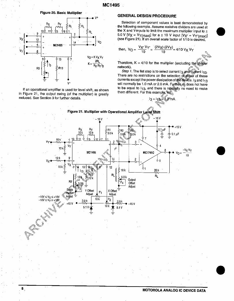
Figure 20. Basic Multiplier
~ v+Rx Ry
‘RL
9
{: :“
RL2
“xt tQ
1214
. ‘,, ,
=:1Vo
l:i -
‘4, .- MC1495 -t
“y
3 13 7VO=KVx Vy
t
‘~
2RL13 K=—
Rx Ry 13R3 R13
“-
If an operational amplifier is used for level shift, as shownin Figure 21, the output swing (of the multiplier) is greatlyreduced. See Section 3 for further details.
GENERAL DESIGN PROCEDURE
Selection of component values is best demonstrated bythe following example. Assume resistive dividers are used atthe X and Y-inputs to limit the maximum multiplier input to ~5.0 V [VX = VY(ma~)] for a * 10 V input [V~”= V~(max)] ●(see Figure 21). If an overall scale factor of 1/1O is desired,
Vy Vy (2VX) (2VY)= 4/1o Vx VYthen, VO= ~= ,0
,:!$,sg:.;y.;:<ti,
,(,. ~,. ~ ,:,.. ~
Therefore, K = 4/10 for the multiplier (excluding t~~$~J&~rnetwork). .,. “.*...~.<:x{L~....1.:..$?
Step 7. The fist step is to select current 13,@&~~:@ent 113.There are no restrictions on the selectionA~:,@fiher of thesecurrents except the power dissipation of,~e~~~e. 13and113will normally be 1.0 mA or 2.0 mA. Furth’&{x~$ does not haveto be equal to 113, and there is &&ily no need to makethem different. For this exampl$’h$t~
.,
‘“v+T-’5V—=
,.
-“x “y10
8., MOTOROLA ANALOG IC DEVICE DATA

MC1495
To set currents 13 and 113 to the desired value, it is onlynecessa~ to connect a resistor between Pin 13 and ground,and between Pin 3 and ground. From the schematic shown inFigure 3, it can be seen that the resistor values necessary aregiven by:
R13+500Q=’V-’;7V
R3 +500 Q =’v-’ ~7 v13
14.3V or R13= 13.8 kQLet V–=–15V, then R13+500=—1.0 mA
Let R13 = 12 kQ. Similarly, R3 = 13.8 W, let R3 = 15 kQ
However, for applications which require an accurate scalefactor, the adjustment of R3 and consequently, 13, offers aconvenient method of making a final trim of the scale factor.For this reason, as shown in Figure 21, resistor R3 is shownas a fixed resistor in series with a potentiometer.
For applications not requiring an exact scale factor(balanced modulator, frequency doubler, AGC amplifier, etc.)Pins 3 and 13 can be connected together and a singleresistor from Pin 3 to ground can be used. In this case, thesingle resistor would have a value of 1/2 the above calculatedvalue for R13.
Step 2. The next step is to select RX and Ry. To insure thatthe input transistors will always be active, the followingconditions should be met:
M<113, !Y <13Rx Ry
voltage. It should also be noticed that the collector voltage oftransistors Q3 and Q4 is at a potential which is twodiode-drops below the voltage at Pin 1. Thus, the voltage atPin 1 should be about 2.0 V higher than the maximum inputvoltage. Therefore, to handle +5.0 V at the inputs, the voltageat Pin 1 must be at least +7.0 V. Let V1 = 9.0 Vdc.
Since the current flowing into Pin 1 is always equal to 213,the voltage at Pin 1 can be set by placing a resistor (RI) fromPin 1 to the positive supply: *,\
*’X,l,$J,$<,.,,.,’~,’$:.‘!,.~1+ts.,
RI = 3.o ~. “$$,$~>$*\ .
,.:~~,\\,~\Note that the voltage at th@Y@~>of transistors Q5, Q6, Q7and Q8 is one diode-dro,@~$@d*the voltage at Pin 1. Thus, inorder that these transi~~~l$~y active, the voltage at Pins 2and 14 should be apWMately halfway between the voltageat Pin 1 and the@#]tlv&supply voltage. For this example, thevoltage at Pin#i:@ 14 should be approximately 11 V.
Step 5. {~o~ti~’applications, such as the multiply, divideand sq~dr~~tit functions, it is usually desirable to conveflthe ..di#~ntial output to a single-ended output voltagere@;~nced to ground. The circuit shown in Figure 22
,:*OFMS this function. It can be shown that the output voltage,:+,,~t~f~Kiscircuit is given by:..... t<<..
A good rule of thumb is to make 13Ry 21.5 Vy(&a$t,~nd113Rx> 1.5VX(max).The largerthe 13Ryand 11~%~~juct inrelation to Vy and VX respectively, the mord%o~’~rate the*:$*,.;:..,~,multiplier will be (see Figures 17 and 18). :~$j.~:,,.$y
Sf~.k## ?O determine what power supply voltage is
n~~~,g~~ fOr this application, attention must be given to the~,g{;~$r’’schematic shown in Figure 3. From the circuit?Wrnatic it can be seen that in order to maintain transistors
~1, Q2, Q3 and Q4 in an active region when the maximuminput voltages are applied (VX = VY = 10 V or VX = 5.0 V,Vy = 5.0 V), their respective collector voltage should be atleast a few tenths of a volt higher than the maximum input
VO = (I2 –114) RL
21X Iy 2vxvyAnd since IA–16 = 12–114 = — —
13 = 13RxRy
then VO =2RL Vx’ Vy’
4Rx Rx 13where, VX’ Vy’ is the voltage at
the input to the voltage dividers.
Figure 22. Level Shift Circuit
Vt
T
RO RO
12<V2
t+
V14 Vo
1144 * –+
RL RL*A,“”
The choice of an operational amplifier for this applicationshould have low bias currents, low offset current, and a highcommon mode input voltage range as well as a high commonmode rejection ratio. The MC1 456, and MC1 741 Coperational amplifiers meet these requirements.
MOTOROLA ANALOG IC DEVICE DATA 9

MCI 495
Referring to Figure 21, the level shift components will bedetermined. When VX = Vy = O,the currents 12and 114will beequal to 113, In Step 3, RL was found to be 20 kQ and in Step4, V2 and V14 were found to be approximately 11 V. From thisinformation RO can be found easily from the followingequation (neglecting the operational amplifiers bias current):
v+_v2 ,,, :.
~.+lq3=—RL RO
And for this example, fiQ+ 1.0 mA=15 V-11 v
RO
Solving for Ro: RO = 2.6 kQ, thus, select RO = 3.0 kQ
For RO = 3.0 kQ, the voltage at Pins 2 and 14 is calculatedto be:
V2=V14=I0.4V,
The linearity of this circuit (Figure 21) is likely to be asgood or better than the circuit of Figure 5. Furtherimprovements are possible as shown in Figure 23 where Ryhas been increased substantially to improve the Y linearity,and RX decreased somewhat so as not to materially affectthe X linearity, This avoids increasing RL significantly in orderto maintain a K of 0.1.
The versatility of the MCI 495 allows the user to tooptimize its petiormance for various input and output signallevels.
OFFSET AND SCALE FACTOR ADJUSTMENT ●Offset Voltages
Within the monolithic multiplier (Hgure 3) transistor base-emitter junctions are typically matched within 1.0 mV andresistors are typically matched within 2Y0. Even with. t%,careful matching, an output error can occur. This out~~~~%};$’is comprised of X-input offset voltage, Y-input offse~~o$~gb,and output offset voltage. These errors can b@sa~%&d tozero with the techniques shown in Figure ~J$t*& termscan be shown analytically by the transfer f,~dqh?’”
VO = K[VX t ~ox A Vx(off)] [Vy + ~o~{~@~j * VOO (1)
Where: K = scale factor,, ~;,. “~w”Vx = “x” input,~~&:Vy = “y” inptif~o*e
~ox = “x” i~~~et voltage~oy = ‘(y’~w offset voltage
VX(OH) .,p$y” ‘iihut offset adjust voltage
‘t(~~$$~:~utput offset voltage.‘$w:$$y*input offset adjust voltage
,. ‘}.>~$., ,~,,i...’,*’ >i,,i,,.,w,,,+~,,,
Figure 23. Multiplier with lmpro~pd ~~earity
-15V●
~2”0k~20k— —
-VxVy10
10 MOTOROLA ANALOG IC DEVICE DATA

MC1 495
X, Y and Output Offset Voltages
Xoxffyox:yFor most dc applications, all three offset adjust
potentiometers (PI, P2, P4) will be necessary. One or moreoffset adjust potentiometers can be eliminated for acapplications (see Figures 28,29, 30, 31).
If well regulated supply voltages are available, the offsetadjust circuit of Figure 13 is recommended. Otherwise, thecircuit of Figure 14 will greatly reduce the sensitivity to powersupply changes.
Scale Factor
The scale factor K is set by P3 (Figure 21). P3 varies 13which inversely controls the scale factor K. It should be notedthat current 13is one-half the current through RI. R1 sets thebias level for Q5, Q6, Q7, and Q8 (see Figure 3). Therefore, tobe sure that these devices remain active under all conditionsof input and output swing, care should be exercised inadjusting P3 over wide voltage ranges (see General DesignProcedure).
Adjustment Procedures
DC APPLICATIONS
Multiply
The circuit shown in Figure 21 may be used to multiplysignals from dc to 100 kHz. Input levels to the actualmultiplier are 5.0 V (max). Wth resistive voltage dividers themaximum could be very large however, for this applicationtwo-to-one dividers have been used so that the ma~{rnuminput level is 10 V. The maximum output level has ak’~en-,/,,$::,+:!?\*designed for 10 V (max). ..,:>:. ,$$:,,.\>$*. ,.,’’’t’t,$.:.,,Squaring Circuit
, >.,*. ...,<,.‘.*~~>,,:<x~~:’.~
.,,. “+$?.If the two inputs are tied together, the rp~&@~function is
squaring; that is VO = KV2 where K is @~JscM# factor. Notethat all error terms can be eli~-~~$>~ith only threeadjustment potentiometers, thus, ell~{n,~ng one of the inputoffset adjustments. Procedurq~~~{ nti%ing with adjustmentsare given as follows: ~~,...:5,,,,+,~:-+,‘<i~,.’.,;~,.:>,,... ..1..,.A. AC Procedure: t$t,.,$~s)’
+.$k:,,,.;>’$1. Connect os@,@,*?~WOkHz, 15 Vpp) to input.2. Monitor g~tpu$qt ~.O kHz with tuned voltmeter
and ad~~$~~ for desired gain. (Be sure to peakresw.~f the voltmeter.)
3. ~#~}v,@meter to 1.0 kHz and adjust P1 for a
*ititim output voltage..,,?~ ~und input and adjust P4 (output offset) for
“’, OVdc output.,,*.,.,,$’ “’t$. ReDeat steps 1 through 4 as necessay.
The following adjustment procedure should be used to null “. w~ ‘.,{~,+
+t.~!i@. DC Procedure:the offsets and set the scale factor for the multiply mode of k; Aoperation, (see Figure 21).
+.,., 1. Set Vx = Vy = O V and adjust P4 (output offset\xt+*}
..,,> \ ~otentiometer) such that Vo = OVdc1. X-Input Offset
.%\::i\.$. 2. Set VX = Vy = 1.0 V and adjust P1 (Y-input offset(a) Connect oscillator (1.0 kHz, 5.0 Vpp sin~{$~~’ potentiometer) such that the output voltage is
to the Y-input (Pin 4). ‘ ~~,+~.j,,4. .,,,, +0.loov.(b) Connect X-input (Pin 9) to ground. t&NJ~@t 3. Set VX = Vy = 10 Vdc and adjust P3 such that(c) Adjust X offset potentiometer (P@}$~~~~bc the output voltage is+ 10 V.
null at the output. .,,.’N’.?,:’~.,:~ .,,“::,+by “ 4. Set Vx = Vy = –1 O Vdc. Repeat steps 1 through
2. Y-Input Offset ,,.., ].s 3 as necessary.(a) Connect oscillator (1.0 kHr$’Wpp sinewave)
to the X-input (Pin 9):<:,,*~,$~!.w;(b) Connect Y-input (Pin~J t$ground.(c) Adjust Y offset ~~~%~~fi’eter (PI ) for an ac null Figure 24. Basic Divide Circuit
at the outputi.. ‘3il\f#
3. Output Offset ~~.g~,l$ “(a) ConneCj @t~~and Y-inputs to ground.(b) Adjup8~M$t offset potentiometer (P4) until
th~ ~&@& voltage (VO) is O Vdc.4. Scqp::%;{ti
(a)$,A ,ly +1 OVdc to both the X and Y-inputs.
t~~~%~~?ust P3 to achieve + 10 V at the output.~$:m;$$peat steps 1 through 4 as necessa~.
,.4,,“~The ability to accurately adjust the MC1495 depends uponthe characteristics of potentiometers P1 through P4.Multi-turn, infinite resolution potentiometers with lowtemperature coefficients are recommended.
Vy
MOTOROLA ANALOG IC DEVICE DATA 11

MCI 495
Divide CircuitConsider the circuit shown in Figure 24 in which the
multiplier is placed in the feedback path of an operationalamplifier. For this configuration, the operational amplifier willmaintain a “virtual ground at the inverting (–) input.Assuming that the bias current of the operational amplifier isnegligible, then II = 12and,
.,
KVXVy -Vz
RI = R2(1)
Solving for Vy,–R1 VZ
vy=— —R2 K VX
-VzIf RI=R2, Vy = —
KVX
–VzIf Rl= KR2, Vy=—
v~
(2)
(3)
(4)
Hence, the output voltage is the ratio of VZ to VX andprovides a divide function. This analysis is, of course, theidealcondition, If the multiplier error is taken into account, theoutput voltage is found to be:
(5)
where AE is the error voltage at the output of the multiplier.Frornthis equation, it is seen that divide accuracy is stronglydependent upon the accuracy at which the multiplier can beset,: particularly at small values of Vy. For example, assumethat RI = R2, and K = 1/1O. For these conditions the outpq~,bf
In terms of percentage error,
percentage error = *I x 100%
or from Equation (5),
AE
‘KVx [1R2 AEPED =
[1R1 VZ ‘. RI.I VZ (7)
.R2 K. VX*,\*’X,l,$J,$<,.,,.,’~,’$:.‘!(:”:1+ts.,
From Equation 7, the percentage error is inversel~~~~~~to voltage VZ (i.e., for increasing values of VZ, the WJ~@’geerror decreases).
,,~+,,,? .~,s(,*‘“ ~!.,1,~.,~‘
A circuit that performs the divide func{~~r~.,~hown inFigure 25. ~!,.>:y’,J.~
~.’yttti,,’,,,<,:N.Nt*J*,
Two things should be emphasized con’~n~@gFigure 25.1. The input voltage (VXI) musk~tgrd~ter than zero and
must be positive. This in@$~kat the current out ofPin 2 of the multipliq$~$dl “&ways be in a directioncompatible with the ~.~$~bf VZ.
2. Pin 2 and 14 of the%f~lier have been interchanged inrespect to th~&&&rat~dnal amplifiers input terminals. Inthis insta,~~:fi~ure 25 differs from the circuitconnectl~Js~Wn in Figure 21; necessitated to insurenega&&f&*ack around the loop.
*..7:,,
A suadted atiiustment procedure for the divide circuit.l,~~e~.~z = OV and adjust the output offset potentiometer
$ (~4) until the output voltage (Vo) remains at some (not,,8,&~~~:decessarily zero) constant value as V~ is varied“:~~~ between +1.0 V and +1 OV.. 2. Keep VZ at OV, set VX’ at +1 OV and adjust the Y input$t”
the divide circuit is given by:offset potentiometer (Pl ) until VO = O V.,\(.*~>:~.,,
~~->..:.,>‘{Yb, 3. Let V~ = VZ and adjust the X-input offset potentiometer●
(P2) until the output voltage remains at some (notnecessarily – 10 V) constant value as VZ = VX’ is variedbetween +1.0 and +1 OV.Keep V~ = VZ and adjust the scale factor potentiometer(P3) until the average value of VO is-10 V as VZ = Vx~ isvaried between +1.0 V and +1 OV.
error woltage of the divide circuit,~~.Q# expected to be a 5. Repeat steps 1 through 4 as necessay to achieve
hundred times the error of theb$i,c;~ultiplier circuit. optimum petiormance.<$!~‘).Y<>$I, ‘~.’,.!.~~\!:;,>,,$s:,’j.,.
●t15vRx Ry , 0.1WF10k 10k
~ ~ ‘“ ~F(~?
t 3 +
6MC1495 MC1741C ● VO
+ ?2
-lo Vzt
vo=~
12 MOTOROLA ANALOG IC DEVICE DATA

MC1495
Hgure 26. Basic Square Root Circuit AC APPLICATIONS
‘Z%zvoL— or _
{
Ivzl“0= y
Square RootA special case of the divide circuit in which the two inputs
to the multiplier are connected together is the square rootfunction as indicated in Figure 26. This circuit may suffer fromlatch-up problems similar to those of the divide circuit. Notethat only one polarity of input is allowed and diode clamping(see Figure 27) protects against accidental latch-up,
This circuit also may be adjusted in the closed-loop modeas follows:
1.
2.
3.
● 4.
The applications that follow demonstrate the versatility ofthe monolithic multiplier. If a potted multiplier is used for thesecases, the results generally would not be as good becausethe potted units have circuits that, although they optimize dcmultiplication operation, can hinder ac applications.
Frequency doubling ofien is done with a diode wherethe fundamental plus a series of harmonic~,,,aregenerated. However, extensive filtering is required t~xinthe desired harmonic, and the second harmo~~,~$tinedunder this technique usually is small in ~~~$L@e andrequires amplification. ?$7...~,};.,,~”.,m.~~,
When a multiplier is used to double f~~qtiti the secondharmonic is obtained directly, exceptq~~~~~pqerm, which canbe removed with ac coupling. :?$;),~~. “
e. = KE2 COS2Q~‘$~ ‘$’~?:t,i:.J~.
,+.f>$v~ji,~“
A potted multiplie~,$afi be used to obtain the doublefrequency tom@’~@nt, but frequency would be limited by itsinternal Iev@*arnplififer. In the monolithic units, theamplifier k $mi&d.
Set VZ to +.01 V and adjust P4 (output offset) for In a @#%~~oubler circuit, conventional + 15 V suppliesVO = +0.316 V, being careful to approach the output aret,:~sed$$n input dynamic range of 5.0 V peak-to-peak isfrom the positive side to preclude the effect of the output alt~~d. The circuit generates wave-forms that are doublediode clamping. fJ$r&$uency; less than 17. distortion is encountered withoutSet VZ to 4.9 V and adjust P2 (X adjust) for ~t~%!$~fing. The configurationhas been successfully used inVo = +3.0 v. .’~.:t,.>~t!..,~:.{
“$;,~;excess of 200 kHz; reducing the scale factor by decreasingSet VZ to -10 V and adjust P3 (scale factor adjust} ‘“ the load resistors can further expand the bandwidth.for VO = +10 V.
~..Figure 29 represents an application for the monolithic
Steps 1 through 3 may be repeated as ne~$s~ to multiplier as a balanced modulator. Here, the audio inputachieve desired accuracy.
,.,\\.~.$f;f~,t$.~.~k.$ signal is 1.6 kHz and the carrier is 40 kHz.
MC1495 I I I I MC1741CL
T● VO
tt-
..t:.i’s,
i
‘“ist~:?;10 k 3
LI ~ ~’
13 8
~
12 - Al &,,,..,,J,AA.
~ 13k —13k
● “z12 k 20 k
)kRL
P. To Offset 5.0 k outputP4 ofls~t
Factor ~-lo<vz<tov
,J!..-,— (See H~ure13) Adjust
MOTOROLA ANALOG !C DEVICE DATA 13

MC1495
Figure 28. Frequency Doubler
Ry RX Vcc +15 v8.2 k 8.2 k
4
E COS mt
(< 5.0 Vpp) 2 3.3 k
Offset Y ~MC1495
R1Adjust .
12 14 3.3 k
~ 3 13 7 *cl’
‘m
‘SelectE2
6,8 k 1,0 pFe.= To cos 2 wt
J
u-15V
When two equal cosine waves are applied 10X and Y, the resultis a wave shape of twice the input frequency, For ttis examplethe input was a 10 kHz signal, output wes 20 kHz,
Figure 29’. Balanced Modulator
(A)
ey =
ex =
ECOS Omt
ECOS Ott
The defining equation for balanced modulation is
K(EmCOS Wmt) (EC COS @et)=
* [ COS (Oc+Qm)t+ COS (Oc- Om) t ]
where mc is the carrier frequency, ~m is the modulatorfrequency and K is the multiplier gain constant.
AC coupling at the output eliminates the need for le~~atranslation or an operational amplifier; a higher op$~a~~frequency results. ,,\. .:$+... -t~}?
A problem common to communications is to. &R/&t~~heintelligence from single-sideband received si~,$b~ne ssbsignal is of the form: .,*>s. .1:$,. *.<*.
essb = A cos (Oc + m~~$~r?”
and if multiplied by the appropriate c~,rfi&@~#veform, cos met,.,<
essbecarfier = + [Cos (2~’*k)t + Cos (WC}t ].~ :. ;p.,:+\T\,+\\*!t,.$$::>~1.If the frequency of the ~l~;l~~ited carrier signal (wc) is
ascetiained in advance,’<~~~:@signer can insert a low passfilter and obtain the ,~W2)’’&oswct) term with ease. He/shealso can use an o~”&@”*al amplifier for a combination levelshift-active filte~$~~~% external component. But in pottedmultipliers, ~de~.ij$~he frequency range can be covered, theoperational’<~plifier is inside and not accessible, so the usermust ~~ept t~e level shiting provided, and still add a lowpas~%{~e~s
.,
,..x~~de Modulation““l~~~he multiplier performs amplitude modulation, similar to,$,~~lanced modulation, when a dc term is added to the
* modulating signal with the Y-offset adjust potentiometer (seeFigure 30). ●
Here, the identity is:
Em(l + m cos ~mt) Ec cos ~ct = KEmEccos ~ct +
KEmEcm
2[ COS(Wc + Wm)t + COS (WC - Wm) t]
where m indicates the degrees of modulation. Since m isadjustable, via potentiometer P1, 1007. modulation ispossible. Wthout extensive tweaking, 960/0 modulation maybe obtained where @c and ~m are the same as in thebalanced modulator example.
Offset YAdjust x
Linear Gain ControlTo obtain linear gain control, the designer can feed to one
of the two MC1495 inputs a signal that will vary the unit’sgain. The following example demonstrates the feasibility ofthis application. Suppose a 200 kHz sinewave, 1,0 Vpeak-to-peak, is the signal to which a gain control will beadded. The dynamic range of the control voltage VC is OV to+1.0 V. These must be ascertained and the proper values ofR.x and Ry can be selected for optimum performance. For the200 kHz operating frequency, load resistors of 100 Q werechosen to broaden’the operating bandwidth of the multiplier,but gain was sacrificed, It maybe made up with an amplifieroperating at the appropriate frequency (see Figure 31).
14 MOTOROLA ANALOG IC DEVICE DATA

MC1 495
figure 30. Amplitude Modulation
ey = EcosOmt
ex = Ecosomt
Y.ModulationA~ust
OffsetAdjust
fly Rx vcc=t15v8.2k 8.2k
4● I
9 RL1● &
.Y !MC1495
x 12 14
34 13+ 47
ex,ey <5.0VPP
rd
‘Select Je.
6.8k I.OKFT
The signal is applied to the unit’s Y-input. Since the totalinput range is limited to 1.0 Vpp, a 2.0 V swing, a currentsource of 2.0 mA and an Ry value of 1.0 kQ is chosen. Thistakes best advantage of the dynamic range and insureslinear operation in the Y-channel.
Since the X-input varies between Oand +1.0 V, the currentsource selected was 1.0 mA, and the RX value chosenwas 2.0 kQ. This also insures linear operation over theX-input dynamic ~ange. Choosing RL = 100 assures wide—bandwidth operation. -
Y“ Y
T 451
i
2 100
100
14
.~,,,~~N2 in the numerator of the equation is missing in this scale“~~~hctor expression because the output is single-ended and ac
,{:t~~‘“ coupled.
Linear Gain Control
1,25
1,0
-= 0.75Z=o> 0.5
0.251 I
y~= 1.OV200k~z
! 1 1 1 I 1
VAGC(V)1.2
MOTOROLA ANALOG IC DEVICE DATA 15

MC1495
OUTLINE DIMENSIONS
i
.,“\.<w ‘+,.,.,.
Motorola ~se~~~fie right to make changes without futiher notice to any products herein. Motorola makes no warranty, representation or guarantee regardingthe sC~~@~~{#,@tsproducts for any pafiicular purpose, nor does Motorola aesume any liability arising out of the application or use of any product or circuit,and,~~~~?]]y disclaims any and all liability, including without limitation consequential or incidental damages. ‘Typica~ parameters can and do va~ in different~~lld~ons. All operating parameters, including ‘Typicals” must be validated for aach customer application by customer’s technical expefls. Motorola doss
~@*bY anY Iicenae under its Patent fights nor the fights of others. Motorola products are not dasigned, intended, or authorized for use as components ins~~ams intended for surgical implant into the body, or other applicafiona intended to suppofl or sustain life, or for any other application in which the failure ofth&Motorola product could creata a situation where personal injury or death may occur. Should Buyer purchase or use Motorola products for any suchunintended or unauthorized application, Buyar shall indemnify and hold Motorola and its officers, employees, subsidiatias, affiliates, and distributors harmlessagainst all claims, costs, damages, and expanses, and reasonable attorney faes arising out of, diractly or indirectly, any claim of parsonal injury or deathassociated with such unintended or unauthorized usa, even if such claim alleges that Motorola was negligent regarding tha design or manufacture of the part.Motorola and @ are registered trademarks of Motorola, Inc. Motorola, Inc. is an Equal Opportunity/Afirmative Action Employer.
How to reach us:USA/ EUROPE: Motorola Literature Mstfibution;PO. Box 20912; Phoenix, Arizona 85036, 14W1–2M7
JAPAN Nippon Motorola Ltd.; TatsumWPWLDC, Toshikateu Otsuki,6FSeibWufsuryWanter, >142Tabumi Kottiu, To~olW, Japan. OW21W15
MFAX: [email protected]. mot.com –TOUCHTONE (602) 2&609 HONG KONG: Motorola Semiconductors H.K. Ltd.; 8B Tai Ping industrial Park,INTERNET htfp://Design-NET.com 51 Ting Kok Road, Tai Po, N.T, Hong Kong. 652-26629298
@M=OROLA
o 1PHX3602H PRl~EDIN USA 9/95 IMPERIALLITHO 14904 4.500 L,N/lNTYC~M MC14951D
llllllllllllllllllllllllllllllllllllllllllllllllll


![Research Article Comparison of 6 Diode and 6 Transistor ...downloads.hindawi.com/archive/2016/8039679.pdf · H mixer with diodes [], a four-quadrant multiplier [] modi ed by us, a](https://img.dokumen.tips/doc/110x75/603abef9ee0b5616606901e7/research-article-comparison-of-6-diode-and-6-transistor-h-mixer-with-diodes.jpg)