Embed Size (px)
Citation preview

Linear Four−Quadrant Multiplier
The MC1494 is designed for use where the output voltage is a linearproduct of two input voltages. Typical applications include: multiply,divide, square root, mean square, phase detector, frequency doubler,balanced modulator/ demodulator, electronic gain control.
The MC1494 is a variable transconductance multiplier with internallevel−shift circuitry and voltage regulator. Scale factor, input offsetsand output offset are completely adjustable with the use of fourexternal potentiometers. Two complementary regulated voltages areprovided to simplify offset adjustment and improve power supplyrejection.• Operates with ±15 V Supplies
• Excellent Linearity: Maximum Error (X or Y) ±1.0 %
• Wide Input Voltage Range: ±10 V
• Adjustable Scale Factor, K (0.1 nominal)
• Single−Ended Output Referenced to Ground
• Simplified Offset Adjust Circuitry
• Frequency Response (3.0 dB Small−Signal): 1.0 MHz
• Power Supply Sensitivity: 30 mV/V typical
0
+
k =110
X
Y KXY
E
o
r E
, L
INE
AR
ITY
ER
RO
R (%
)R
XR
Y
TA, AMBIENT TEMPERATURE (°C)
1.00
0.75
0.50
0.25
0−50 0 50 125−10 −8.0 −6.0 −4.0 −2.0 0 2.0 4.0 6.0 8.0 10
VX, INPUT VOLTAGE (V)
−10
−8.0
−4.0
−2.0
2.0
−6.0
4.0
6.0
8.0
10
, OU
TPU
T V
OLT
AG
E (V
)OV
Figure 1. Multiplier Transfer Characteristic Figure 2. Linearity Error versus Temperature
−25 25 75 100
ON Semiconductor
Semiconductor Components Industries, LLC, 2004
June, 2004 − Rev. XXX1 Publication Order Number:
MC1494/D
LINEAR FOUR−QUADRANTMULTIPLIER INTEGRATED
CIRCUIT
SEMICONDUCTORTECHNICAL DATA
MC1494
P SUFFIXPLASTIC PACKAGE
CASE 648C
ORDERING INFORMATION
PackageTested Operating
Temperature RangeDevice
MC1494P TA = 0° to + 70°C Plastic DIP
1
16

MC1494
http://onsemi.com2
MAXIMUM RATINGS (TA = + 25°C, unless otherwise noted.)
Rating Symbol Value Unit
Power Supply Voltages ± V ± 18 Vdc
Differential Input Signal V9−V6V10−V13
±|6 + I1RY|<30±|6 + I1RX|<30
Vdc
Common Mode Input VoltageVCMY = V9 = V6VCMX = V10 = V13
VCMYVCMX
±11.5±11.5
Vdc
Power Dissipation (Package Limitation)TA = + 25°CDerate above TA = + 25°C
PD1/θJA
1.2520
WmW/°C
Operating Temperature Range TA 0 to +70 °C
Storage Temperature Range Tstg − 65 to +150 °C
ELECTRICAL CHARACTERISTICS (±V = ±15 V, TA = + 25°C, R1 = 16 kΩ, RX = 30 kΩ, RY = 62 kΩ, RL = 47 kΩ, unless otherwise noted.)
Characteristics Figure Symbol Min Typ Max Unit
LinearityOutput error in percent of full scale−10 V <VX < +10 V (VY = ±10 V)−10 V <VY < +10 V (VX = ±10 V)TA = +25°CTA = Thigh or Tlow (Note 1)
3 ERX or ERY
−−
±0.5−
±1.0±1.3
%
InputVoltage Range (VX = VY = Vin)Resistance (X or Y Input)Offset Voltage (X Input) (Note 1)
(Y Input) (Note 1)Bias Current (X or Y Input)Offset Current (X or Y Input)
4, 5, 6VinRin
|Viox||Vioy|
Ib|Iio|
±10−−−−−
−3000.20.81.050
−−
2.52.52.5400
VpkMΩV
µAnA
OutputVoltage Swing CapabilityImpedanceOffset Voltage (Note 1)Offset Current (Note 1)
5, 6VORO
|VOO||IOO|
±10−−−
−8501.225
−−
2.552
VpkkΩV
µA
Temperature Stability (Drift)TA = Thigh to Tlow
Output Offset (X = 0, Y = 0) Voltage
Current
X Input Offset (Y = 0)
Y Input Offset (X = 0)
Scale Factor
Total DC Accuracy Drift (X = 10, Y = 10)
−
|TCVOO||TCIOO||TCViox||TCVioy||TCK||TCE|
−−−−−−
1.3270.31.50.070.09
−−−−−−
mV/°CnA/°CmV/°C
%/°C
Dynamic ResponseSmall Signal (3.0 dB)
Power Bandwidth (47 k)3° Relative Phase Shift1% Absolute Error
7BW3dB (X)BW3dB (Y)
PBWfφfθ
−−−−−
0.81.044024030
−−−−−
MHz
kHz
Common ModeInput Swing (X or Y)Gain (X or Y)
8CMVACM
±10.5−
−− 65
−−
VpkdB
Power SupplyCurrent
Quiescent Power DissipationSensitivity
9Id+Id−PDS+S−
−−−−−
6.06.51851330
1212350100200
mAdc
mWmV/V
Regulated Offset Adjust VoltagesPositive/NegativeTemperature Coefficient (VR+ or VR−)Power Supply Sensitivity (VR+ or VR−)
9VR+, VR−
TCVRSR+, SR−
3.5−−
4.30.030.6
5.0−−
VdcmV/°CmV/V
NOTE: 1. Offsets can be adjusted to zero with external potentiomers. THigh = +70°C, TLow = 0°C

MC1494
http://onsemi.com3
47 k
9
13
10
I10
9
13I13
10
8.2 k 24
6
9
13
10
8.2 k 24
13
10
[ e2Y
e1Y
− 2 MΩ
RY
VY
Figure 3. Linearity Figure 4. Input Resistance
Figure 5. Offset Voltages, Gain Figure 6. Input Bias Current/Input OffsetCurrent, Output Resistance
Figure 7. Frequency Response Figure 8. Common Mode
To A
10 V
+
−
f = 20 Hz
VX 10E = 20 Vpp
13
9
6
11 12 7 8 1 314
15+15 V
0.1 µF
−15 V
RX = 30 k RY = 62 k R1 =16 k
22 k 50 k
VO
MC1456
10 k 10 k
A −
+
−
+
0.1 µF
Eo
50 k
20 k
20 k
VR 2VR
Adjust RL for a null in EoRL
Linearity, Error =Eo(peak)
ES(peak)
11 12 7 8 1 3
30 k 62 k16 k
MC1494
1.0 M
f = 20 Hz e2X
1.0 M
−
+
−
+
1.0 M
6
e1X
e1Y
e2Y
1.0 M
4 2
8.2 k
RX 14
15
5
VO
+15 V
0.1 µF
−15 V
0.1 µF
Rin X = [ ]e1Xe2X
Rin Y = ]− 2
13
9
6
11 12 7 8 1 314
I5
15+15 V
0.1 µF
−15 V
30 k 62 k 16 k
22 k 50 k
VO
MC1456
−
+
50 k
20 k
20 k
RL
RX RY10
VY off
VX off
4
VO off
5
I15
6I6
I9
6
9
8.2 k
14
15
5
+15 V
−15 V
47 k
CO = 3.0 pF
RL CMVY(20 Hz)
51
VX
VY
VX
VY
MC1494
10 k
MC1456
5 0.1 µF
MC1494
0.1 µF
11 12 7 8 1 3
30 k 62 k 16 k
RX RY
24
0.1 µF
0.1 µF
15
5
+15 V
−15 V
0.1 µF
0.1 µF
14
47 k
VO11 12 7 8 1 3
30 k 62 k 16 k
RX RY
11 12 7 8 1 3
30 k 62 k 16 k
RX RY14
15
5
+15 V
−15 V
47 kRO
0.1 µF
0.1 µF
4
I5
I15
VO
VO
+
+
−
− − +
− +
MC1494
+−
+
+
−
−
−
2
+
+
−
+
−
+−
+
−
+
−
−
+
−
+
MC1494MC1494
+−
MΩ

MC1494
http://onsemi.com4
Figure 9. Power Supply Sensitivity Figure 10. Burn−In
14
5
+15 V
VS
100 HzVR− VR+
−15 V
VO
16NC
VO
15
14
13
12
11
10
9Vin − +10 V
16 k 1
2
3
4
5
6
7
862 k
−15 V
30 k8.2 k 24
13
10
6
9
11 12 7 8 1 3
30 k 62 k 16 k
RX RY
47 k15 0.1 µF
0.1 µF
8.2 k
0.1 µF
+15 V
47 kMC1494MC1494
+−−
−
+
+
Figure 11. Frequency Response of Y Inputversus Load Resistance
Figure 12. Frequency Response of X Inputversus Load Resistance
0.4
0.3
0.2
0.1
0
2.0 4.0 6.0 8.0 10
4.0 8.0 12 16 20
RX (kΩ)
RY (kΩ)
15
10
5.0
0
−5.0
−10
−15
−20103 104 105 106 107
f, FREQUENCY (Hz)
RE
LATI
VE
GA
IN (d
B)
Figure 13. Linearity versus R X or RY with K = 1 Figure 14. Linearity versus R X or RY with K = 1/10
103 104 105 106 107
f, FREQUENCY (Hz)
15
10
5.0
0
−10
−15
−20
RE
LATI
VE
GA
IN (d
B)
0.6
0.5
0.4
0.3
0.220 30 40 50
40 60 80 100
E
or
E
, L
INE
AR
ITY
ER
RO
R (%
)R
XR
Y
RX (kΩ)
RY (kΩ)
−5.0
E
or
E
, L
INE
AR
ITY
ER
RO
R (%
)R
XR
Y
VY = 1.0 Vrms, VX = 10 VdcRX = 30 kΩ, RY = 62 kΩCO = 6.0 pF
CO = 6.0 pFRX = 30 kΩ, RY = 62 KΩVX = 1.0 Vrms, VY = 10 Vdc
RL = 1.0 kΩ
RL = 47 kΩ
RL = 33 kΩ
RL = 10 kΩRL = 1.0 kΩ
RL = 33 kΩ
RL = 47 kΩ
RL = 10 kΩ
RL Adjusted for K = 1
Vin = 2.0 Vpp Vin = 20 VppRL Adjusted for K = 1/10

MC1494
http://onsemi.com5
1
2
20
0
10
100 1.0 k 10 k 100 kf, FREQUENCY (Hz)
Figure 15. Large Signal Voltage versus Frequency Figure 16. Scale Factor (K) versus Temperature
0.108
0.106
0.104
0.102
0.1
0.098
0.096
0.094
−55 −35 −15 5.0 25 45 65 85 105 125
TA, AMBIENT TEMPERATURE (°C)
K, S
CA
LE F
AC
TOR
V
, OU
TPU
T V
OLT
AG
E (V
pp)
O
145
1
2
With MC1456 Buffer Op Amp
No Op Amp, RL = 47 kΩ
K Factor Adjusted for 1/10 at 25°C)
CIRCUIT DESCRIPTION
IntroductionThe MC1494 is a monolithic, four−quadrant multiplier
that operates on the principle of variable transconductance.It features a single−ended current output referenced toground and provides two complementary regulated voltagesfor use with the offset adjust circuits to virtually eliminatesensitivity of the offset voltage nulls to changes in supplyvoltages.
As shown in Figure 17, the MC1494 consists of amultiplier proper and associated peripheral circuitry toprovide these features.
RegulatorThe regulator biases the entire MC1494 circuit making it
essentially independent of supply variation. It also providestwo convenient regulated supply voltages which can be usedin the offset adjust circuitry. The regulated output voltage atPin 2 is approximately + 4.3 V, while the regulated voltageat Pin 4 is approximately − 4.3 V. For optimum temperaturestability of these regulated voltages, it is recommended that|I2| = |I4| = 1.0 mA (equivalent load of 8.6 kΩ). As will beshown later, there will normally be two 20 kΩpotentiometers and one 50 kΩ potentiometer connectedbetween Pins 2 and 4.
The regulator also establishes a constant current referencethat controls all of the constant current sources in theMC1494. Note that all current sources are related to currentI1 which is determined by R1. For best temperaturesperformance, R1 should be 16 kΩ so that I1 ≈ 0.5 mA for allapplications.
MultiplierThe multiplier section of the MC1494 (center section of
Figure 17) is nearly identical to the MC1495 and is discussedin detail in Application Note AN489, Analysis and BasicOperation of the MC1495. The result of this analysis is thatthe differential output current of the multiplier is given by:
RXRYI1
2VX VYIA − IB = ∆I
Therefore, the output is proportional to the product of thetwo input voltages.
Differential Current ConverterThis portion of the circuitry converts the differential
output current (IA −IB) of the multiplier to a single−endedoutput current (IO); IO = IA − IB
IO =2VX VY
RXRYI1or
The output current can be easily converted to an outputvoltage by placing a load resistor RL from the output (Pin 14)to ground (Figure 19) or by using an op amp as acurrent−to−voltage converter (Figure 18). The result in bothcircuits is that the output voltage is given by:
where, K (scale factor) =2RL
RXRYI1
VO =2RL VX VY
= KVXVYRXRYI1
DC OPERATION
Selection of External ComponentsFor low frequency operation the circuit of Figure 18 is
recommended. For this circuit, RX = 30 kΩ, RY = 62 kΩ,R1 = 16 kΩ and, hence, I1 ≈ 0.5 mA. Therefore, to set thescale factor (K) equal to 1/10, the value of RL can becalculated to be:
=1
10K =
2RL
RXRYI1
or RL =RXRYI1
(2) (10)=
(30 k) (62 k) (0.5 mA)
20
RL = 46.5 k
Thus, a reasonable accuracy in scale factor can beachieved by making RL a fixed 47 kΩ resistor. However, ifit is desired that the scale factor be exact, RL can becomprised of a fixed resistor and a potentiometer as shownin Figure 18.

MC1494
http://onsemi.com6
Figure 17. Internal Schematic(Recommended External Circuitry is Depicted within Dotted Lines)
Block Diagram15+V
2 +4.3 V+ VR
3
4
−VR−4.3 V
1
R1
Current and VoltageRegulator 9
6VY
+
−
+
−
Four QuadrantMultiplier
IA
IB1013
VX
7 8 11 12
DifferentialCurrent
Converter
14
IO(IO = IA − IB)
5−V
15
+V
I1 ConstantCurrentSourceControl
+9.4 V
8.7 k
8.7 k
7.2 k
7.2 k
−9.4 V
I13 I1
4 −4.3 V
2
3
+4.3 V+8.7 V
R1I1
I1
2.4 V
Simplified CircuitSchematic 2 I1 1.7 V 2 I1
14IO
IA
IB
9
6
VY
7 8
RY I1I1 I1RX I1
13
10VX
500 500
−V5
15
+V
500 500 5.4 k 500
3.0 k
7.2 k
8.7 k
8.7 k
7.2 k
7.2 k
2+ VR
1
3
R1GND
+VR
4
5−V
Complete CircuitSchematic
9
VY
6
10 k7
8
RY
10 k 10 k 10 k
10
+
13
VX
12
11
RX
500 500
Regulator MultiplierDifferential
Current Converter
IO14
500 500 500 500
2.0 k 2.0 k
10 pF 10 pF
500 500 500 500 500500 500 500 500
11 12
RY RX
+ VR
−VR
This device contains 44 active transistors.
MC1494
http://onsemi.com7
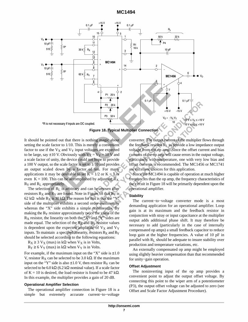
Figure 18. Typical Multiplier Connection
+15 V +15 V
15 5
RL
50 k 22 k
10 pF
2
3
3
14
1
R116 k
P4
6
4
7
10
11
30 k RX12
13
9
8
7
6
4 2P1 20 k
P2
P3
20 k
50 k
R*510
10 pF
510
10 pFR*
62 k RY
MC1494
+
+−−
+
−
+
−
+
MC1456 VO
0.1 µF
+15 V −15 V
VO = −VX VY
10−10 V ≤ VX ≤ +10 V
−10 V ≤ VY ≤ +10 V*R is not necessary if inputs are DC coupled.
0.1 µF
0.1 µF0.1 µF
VX
VY
It should be pointed out that there is nothing magic aboutsetting the scale factor to 1/10. This is merely a convenientfactor to use if the VX and VY input voltages are expectedto be large, say ±10 V. Obviously with VX = VY = 10 V anda scale factor of unity, the device could not hope to providea 100 V output, so the scale factor is set to 1/10 and providesan output scaled down by a factor of ten. For manyapplications it may be desirable to set K = 1/2 or K = 1 oreven K = 100. This can be accomplished by adjusting RX,RY and RL appropriately.
The selection of RL is arbitrary and can be chosen afterresistors RX and RY are found. Note in Figure 18 that RY is62 kΩ while RX is 30 kΩ. The reason for this is that the “Y”side of the multiplier exhibits a second order nonlinearitywhereas the “X” side exhibits a simple nonlinearity. Bymaking the RY resistor approximately twice the value of theRX resistor, the linearity on both the “X” and “Y” sides aremade equal. The selection of the RX and RY resistor valuesis dependent upon the expected amplitude of VX and VYinputs. To maintain a specified linearity, resistors RX and RYshould be selected according to the following equations:
RX ≥ 3 VX (max) in kΩ when VX is in Volts,RY ≥ 6 VY (max) in kΩ when VY is in Volts.
For example, if the maximum input on the “X” side is ±1.0V, resistor RX can be selected to be 3.0 kΩ. If the maximuminput on the “Y” side is also ±1.0 V, then resistor RY can beselected to be 6.0 kΩ (6.2 kΩ nominal value). If a scale factorof K = 10 is desired, the load resistor is found to be 47 kΩ.In this example, the multiplier provides a gain of 20 dB.
Operational Amplifier SelectionThe operational amplifier connection in Figure 18 is a
simple but extremely accurate current−to−voltage
converter. The output current of the multiplier flows throughthe feedback resistor RL to provide a low impedance outputvoltage from the op amp. Since the offset current and biascurrents of the op amp will cause errors in the output voltage,particularly with temperature, one with very low bias andoffset currents is recommended. The MC1456 or MC1741are excellent choices for this application.
Since the MC1494 is capable of operation at much higherfrequencies than the op amp, the frequency characteristics ofthe circuit in Figure 18 will be primarily dependent upon theoperational amplifier.
StabilityThe current−to−voltage converter mode is a most
demanding application for an operational amplifier. Loopgain is at its maximum and the feedback resistor inconjunction with stray or input capacitance at the multiplieroutput adds additional phase shift. It may therefore benecessary to add (particularly in the case of internallycompensated op amps) a small feedback capacitor to reduceloop gain at the higher frequencies. A value of 10 pF inparallel with RL should be adequate to insure stability overproduction and temperature variations, etc.
An externally compensated op amp might be employedusing slightly heavier compensation than that recommendedfor unity−gain operation.
Offset AdjustmentThe noninverting input of the op amp provides a
convenient point to adjust the output offset voltage. Byconnecting this point to the wiper arm of a potentiometer(P3), the output offset voltage can be adjusted to zero (seeOffset and Scale Factor Adjustment Procedure).
MC1494
http://onsemi.com8
The input offset adjustment potentiometers, P1 and P2will be necessary for most applications where it is desirableto take advantage of the multiplier’s excellent linearitycharacteristics. Depending upon the particular application,some of the potentiometers can be omitted (see Figures 19,21, 24, 26 and 27).
Offset and Scale Factor Adjustment ProcedureThe adjustment procedure for the circuit of Figure 18 is:
A. X Input Offset1. Connect oscillator (1.0 kHz, 5.0 Vpp sinewave)
to the ‘‘Y’’ input (Pin 9).2. Connect ‘‘X’’ input (Pin 10) to ground.3. Adjust X−offset potentiometer, P2 for an AC null
at the output.B. Y Input Offset
1. Connect oscillator (1.0 kHz, 5.0 Vpp sinewave) to the ‘‘X’’ input (Pin 10).
2. Connect ‘‘Y’’ input (Pin 9) to ground.3. Adjust Y−offset potentiometer, P1 for an AC null
at the output.C. Output Offset
1. Connect both ‘‘X’’ and ‘‘Y’’ inputs to ground.2. Adjust output offset potentiometer, P3 until the
output voltage VO is 0 Vdc.D. Scale Factor
1. Apply +10 Vdc to both the ‘‘X’’ and ‘‘Y’’ inputs.2. Adjust P4 to achieve −10 V at the output.3. Apply −10 Vdc to both ‘‘X’’ and ‘‘Y’’ inputs and
check for VO = −10 V.E. Repeat steps A through D as necessary.
The ability to accurately adjust the MC1494 is dependent onthe offset adjust potentiometers. Potentiometers should beof the “infinite” resolution type rather than wirewound. Fineadjustments in balanced−modulator applications mayrequire two potentiometers to provide “coarse” and “fine”adjustment. Potentiometers should have low temperaturecoefficients and be free from backlash.
Temperature StabilityWhile the MC1494 provides excellent performance in
itself, overall performance depends to a large degree on thequality of the external components. Previous discussionshows the direct dependence on RX, RY and RL and indirectdependence on R1 (through I1). Any circuit subjected totemperature variations should be evaluated with theseeffects in mind.
Bias CurrentsThe MC1494 multiplier, like most linear ICs, requires a
DC bias current into its input terminals. The device cannotbe capacitively coupled at the input without regard for thisbias current. If inputs VX and VY are able to supply the smallbias current (≈ 0.5 µA) resistors R can be omitted (see Figure18). If the MC1494 is used in an AC mode of operation andcapacitive coupling is used the value of resistor R can be anyreasonable value up to 100 kΩ. For minimum noise andoptimum temperature performance, the value of resistor Rshould be as low as practical.
Parasitic OscillationWhen long leads are used on the inputs, oscillation may
occur. In this event, an RC parasitic suppression networksimilar to the ones shown in Figure 18 should be connecteddirectly to each input using short leads. The purpose of thenetwork is to reduce the “Q” of the source−tuned circuitswhich cause the oscillation.
Inability to adjust the circuit to within the specifiedaccuracy may be an indication of oscillation.
AC OPERATION
GeneralFor AC operation, such as balanced modulation,
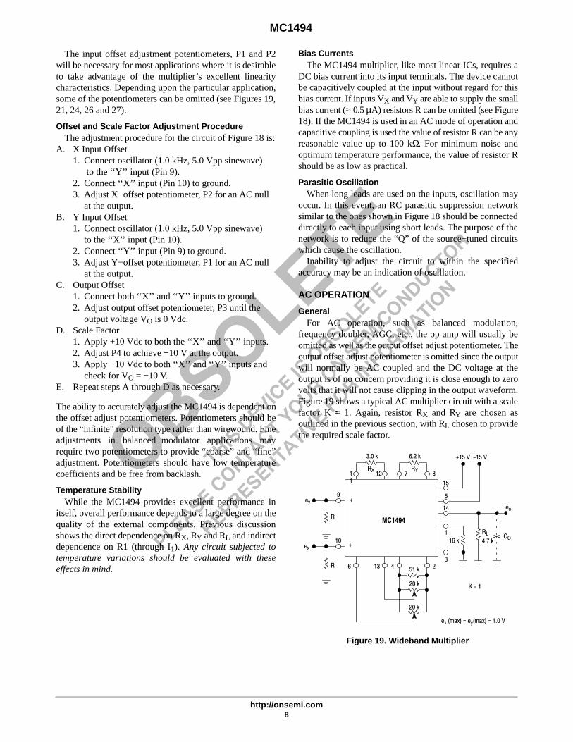
frequency doubler, AGC, etc., the op amp will usually beomitted as well as the output offset adjust potentiometer. Theoutput offset adjust potentiometer is omitted since the outputwill normally be AC coupled and the DC voltage at theoutput is of no concern providing it is close enough to zerovolts that it will not cause clipping in the output waveform.Figure 19 shows a typical AC multiplier circuit with a scalefactor K ≈ 1. Again, resistor RX and RY are chosen asoutlined in the previous section, with RL chosen to providethe required scale factor.
3.0 k 6.2 k
11
RX12 7 8
RY
+15 V −15 V
15
5
14
1
3
16 k
RL
4.7 kCO
eo
MC1494
+
+
9
R
10
ey
ex
R 6 13 4 51 k
20 k
20 k
2
K = 1
ex (max) = ey(max) = 1.0 V
Figure 19. Wideband Multiplier
MC1494
http://onsemi.com9
The offset voltage then existing at the output will be equalto the offset current times the load resistance. The outputoffset current of the MC1494 is typically 17 µA and 35 µAmaximum. Thus, the maximum output offset would be about160 mV.
BandwidthThe bandwidth of the MC1494 is primarily determined by
two factors. First, the dominant pole will be determined bythe load resistor and the stray capacitance at the outputterminal. For the circuit shown in Figure 19, assuming a totaloutput capacitance (CO) of 10 pF, the 3.0 dB bandwidthwould be approximately 3.4 MHz. If the load resistor were47 kΩ, the bandwidth would be approximately 340 kHz.
Secondly, a “zero” is present in the frequency responsecharacteristic for both the “X” and “Y” inputs which causesthe output signal to rise in amplitude at a 6.0 dB/octave slopeat frequencies beyond the breakpoint of the “zero”. The“zero” is caused by the parasitic and substrate capacitancewhich is related to resistors RX and RY and the transistorsassociated with them. The effect of these transmission“zeros” is seen in Figures 11 and 12. The reason for thisincrease in gain is due to the bypassing of RX and RY at highfrequencies. Since the RY resistor is approximately twice thevalue of the RX resistor, the zero associated with the “Y”input will occur at approximately one octave below the zeroassociated with “X” input. For RX = 30 kΩ and RY = 62 kΩ,the zeros occur at 1.5 MHz for the “X” input and 700 kHzfor the “Y” input. These two measured breakpointscorrespond to a shunt capacitance of about 3.5 pF. Thus, forthe circuit of Figure 19, the “X” input zero and “Y” inputzero will be at approximately 15 MHz and 7.0 MHzrespectively.
It should be noted that the MC1494 multiplies in the timedomain, hence, its frequency response is found by means ofcomplex convolution in the frequency (Laplace) domain.This means that if the “X” input does not involve afrequency, it is not necessary to consider the “X” sidefrequency response in the output product. Likewise, for the“Y” side. Thus, for applications such as a wideband linearAGC amplifier which has a DC voltage as one input, themultiplier frequency response has one zero and one pole. Forapplications which involve an AC voltage on both the “X”and “Y” side such as a balanced modulator, the productvoltage response will have two zeros and one pole, hence,peaking may be present in the output.
From this brief discussion, it is evident that for ACapplications; (1) the value of resistors RX, RY and RL shouldbe kept as small as possible to achieve maximum frequencyresponse, and (2) it is possible to select a load resistor RLsuch that the dominant pole (RL, CO) cancels the input zero(RX, 3.5 pF or RY, 3.5 pF) to give a flat amplitudecharacteristic with frequency. This is shown in Figures 11and 12. Examination of the frequency characteristics of the“X” and “Y” inputs will demonstrate that for wideband
amplifier applications, the best tradeoff with frequencyresponse and gain is achieved by using the “Y” input for theAC signal.
For AC applications requiring bandwidths greater thanthose specified for the MC1494, two other devices arerecommended. For modulator−demodulator applications,the MC1496 may be used up to 100 MHz. For widebandmultiplier applications, the MC1495 (using small collectorloads and AC coupling) can be used.
Slew−RateThe MC1494 multiplier is not slew−rate limited in the
ordinary sense that an op amp is. Since all the signals in themultiplier are currents and not voltages, there is no chargingand discharging of stray capacitors and thus no limitationsbeyond the normal device limitations. However, it should benoted that the quiescent current in the output transistors is0.5 mA and thus the maximum rate of change of the outputvoltage is limited by the output load capacitance by thesimple equation:
∆VO
CIO
∆TSlew Rate
∆VO =
Thus, if CO is 10 pF, the maximum slew rate would be:
∆T=
0.5 x 10− 3
10 x 10−12= 50 V/µs
This can be improved, if necessary, by the addition of anemitter−follower or other type of buffer.
Phase Vector ErrorAll multipliers are subject to an error which is known as
the phase vector error. This error is a phase error only anddoes not contribute an amplitude error per se. The phasevector error is best explained by an example. If the “X” inputis described in vector notation as;
X= A0°and the “Y” input is described as;
Y= B0°then the output product would be expected to be;
VO= AB0° (see Figure 20)
However, due to a relative phase shift between the ‘‘X’’ and‘‘Y’’ channels, the output product will be given by:
VO = ABφNotice that the magnitude is correct but the phase angle of theproduct is in error. The vector (V) associated with this erroris the ‘‘phase vector error’’. The startling fact about the phasevector error is that it occurs and accumulates much morerapidly than the amplitude error associated with frequencyresponse. In fact, a relative phase shift of only 0.57° will resultin a 1% phase vector error. For most applications, this erroris meaningless. If phase of the output product is not important,then neither is the phase vector error. If phase is important,such as in the case of double sideband modulation or

MC1494
http://onsemi.com10
demodulation, then a 1% phase vector error will represent a1% amplitude error a the phase angle of interest.
X = A 0°Y = B
Vφ
Figure 20. Phase Vector Error
0° AB φ
AB0°
Circuit LayoutIf wideband operation is desired, careful circuit layout
must be observed. Stray capacitance across RX and RYshould be avoided to minimize peaking (caused by a zerocreated by the parallel RC circuit).
DC APPLICATIONS
Squaring CircuitIf the two inputs are connected together, the resultant
function is squaring:VO = KV2
where K is the scale factor (see Figure 21).However, a more careful look at the multiplier’s defining
equation will provide some useful information. The outputvoltage, without initial offset adjustments is given by:
VO = K(VX + Viox −VX off) (VY + Vioy −VY off) + VOO
(Refer to “Definitions” section for an explanation of terms.)
With VX = VY = V (squaring) and defining;∈ x = Viox − Vx (off)∈ y = Vioy − Vy (off)
The output voltage equation becomes:VO = KVx
2+ KVx (∈ x + ∈ y) + K∈ x ∈ y + VOO
−V2
10
9
10
+
+
15
5
14
2
3
−
+
11 12
30 k 62 k
7 8
+15 V −15 V
P4
50 k 22 k
10 pF
MC1456
−15 V +15 V
4
710 pF
510
V
+MC1494
1 3 6 13 4 2
16 k
51 k
20 k
P1
20 k
InputOffset
P3
OutputOffset
6VO =
Figure 21. MC1494 Squaring Circuit
This shows that all error terms can be eliminated with onlythree adjustment potentiometers, eliminating one of theinput offset adjustments. For instance, if the “X” input offsetadjustment is eliminated, ∈ x is determined by the internaloffset (Viox) but ∈ y is adjustable to the extent that the(∈ x+ ∈ y) term can be zeroed. Then the output offsetadjustment is used to adjust the Voo term and thus zero theremaining error terms. An AC procedure for nulling withthree adjustments is:
A. AC Procedure:1. Connect oscillator (1.0 kHz, 15 Vpp) to input.2. Monitor output at 2.0 kHz with tuned voltmeter and
adjust P4 for desired gain ( Be sure to peakresponse of voltmeter).
3. Tune voltmeter to 1.0 kHz and adjust P1 for a minimum output voltage.
4. Ground input and adjust P3 (output offset) for 0 Vdc out.
5. Repeat steps 1 through 4 as necessary.
B. DC Procedure:1. Set VX = VY = 0 V and adjust P3 (output offset
potentiometer) such that VO = 0 Vdc.2. Set VX = VY = 1.0 V and adjust P1 (Y input offset
potentiometer) such that the output voltage is− 0.100 V.
3. Set VX = VY = 10 Vdc and adjust P4 (load resistor)such that the output voltage is −10 V.
4. Set VX = VY = −10 Vdc and check that VO = −10 V.5. Repeat steps 1 through 4 as necessary.
DivideDivide circuits warrant a special discussion as a result of
their special problems. Classic feedback theory teaches thatif a multiplier is used as a feedback element in an operationalamplifier circuit, the divide function results. Figure 22

MC1494
http://onsemi.com11
illustrates the theoretical simplicity of such an approach anda practical realization is shown in Figure 23.
The characteristic “failure” mode of the divide circuit islatch−up. One way it can occur is if VX is allowed to gonegative, or in some cases, if VX approaches zero.
Figure 22 illustrates why this is so. For VX > 0 the transferfunction through the multiplier is noninverting. Its output isfed to the inverting input of the op amp Thus, operation is inthe negative feedback mode and the circuit is DC stable.
+
+
+
+
−VZ
−
KVX VY
VX
MC1494
VO
VZ = −KVXVY
or
VO =−VZ
KVX+
Figure 22. Basic Divide Circuit Using Multiplier
VY
Should VX change polarity, the transfer function throughthe multiplier becomes inverting, the amplifier has positivefeedback and latch−up results. The problem resulting fromVX being near zero is a result of the transfer through themultiplier being near zero. The op amp is then operatingwith a very high closed−loop gain and error voltages canthus become effective in causing latch−up.
The other mode of latch−up results from the outputvoltage of the op amp exceeding the rated common modeinput voltage of the multiplier. The input stage of themultiplier becomes saturated, phase reversal results, and thecircuit is latched up. The circuit of Figure 23 protects againstthis happening by clamping the output swing of the op ampto approximately ± 10.7 V. Five percent tolerance, 10 Vzeners are used to assure adequate output swing but still limitthe output voltage of the op amp from exceeding thecommon mode input range of the MC1494.
Setting up the divide circuit for reasonably accurateoperation is somewhat different from the procedure for themultiplier itself. One approach, however, is to break thefeedback loop, null out the multiplier circuit, and then closethe loop.
Figure 23. Practical Divide Circuit
30 k 62 k
11 12 7 8
RL
50 k 22 k
10 pF
14
1
2
3
6
VO
+15 V −15 V
MC1494
MC1741CP1
1N5240A(10 V)
orEquivalent
VO =−10 VZ
VX
0 < VX < +10 V−10 V ≤ VZ ≤ +10 V
−15 V +15 V
P2 20 k
P3 50 k
P1 20 k 2
10
9
6
316 k
+
+
+
−
VZ
5 15 13 4
10 pF
510
10 pF
510
4
7VX
A simpler approach, since it does not involve breaking theloop (thus making it more practical on a production basis),is:1. Set VZ = 0 V and adjust the output offset potentiometer
(P3) until the output voltage (VO) remains at some (notnecessarily zero) constant value as VX is variedbetween +1.0 V and +10 V.
2. Maintain VZ at 0 V, set VX at +10 V and adjust theY input offset potentiometer (P1) until VO = 0 V.
3. With VX = VZ, adjust the X input offset potentiometer(P2) until the output voltage remains at some (notnecessarily −10 V) constant value as VZ = VX is variedbetween +1.0 V and +10 V.
4. Maintain VX = VZ and adjust the scale factor potentiometer (RL) until the average value of VO is −10 V as VZ = VX is varied between +1.0 V and +10 V.
5. Repeat steps 1 through 4 as necessary to achieveoptimum performance.
Users of the divide circuit should be aware that theaccuracy to be expected decreases in direct proportion to thedenominator voltage. As a result, if VX is set to 10 V and0.5% accuracy is available, then 5% accuracy can beexpected when VX is only 1.0 V.
In accordance with an earlier statement, VX may haveonly one polarity (positive) while VZ may be either polarity.

MC1494
http://onsemi.com12
KVO2 = −VZ
or
VO = |VZ|
K
VZ ≤ 0 V
Figure 24. Basic Square Root Circuit
+
+
+
−VZ
−
KVO2 X
MC1494
VO
+
Square RootA special case of the divide circuit in which the two inputs
to the multiplier are connected together results in the squareroot function as indicated in Figure 24. This circuit too maysuffer from latch−up problems similar to those of the dividecircuit. Note that only one polarity of input is allowed anddiode clamping (see Figure 25) protects against accidentallatch−up.
This circuit too, may be adjusted in the closed−loop mode:1. Set VZ = −0.01 Vdc and adjust P3 (output offset) for
VO = 0.316 Vdc.2. Set VZ to −0.9 Vdc and adjust P2 (“X” adjust) for
VO = +3.0 Vdc.3. Set VZ to −10 Vdc and adjust P4 (gain adjust) for
VO = +10 Vdc.4. Steps 1 through 3 may be repeated as necessary to
achieve desired accuracy.
NOTE: Operation near 0 V input may prove veryinaccurate, hence, it may not be possible to adjust VO to zerobut rather only to within 100 mV to 400 mV of zero.
AC APPLICATIONS
Wideband Amplifier with Linear AGCIf one input to the MC1494 is a DC voltage and a signal
voltage is applied to the other input, the amplitude of theoutput signal can be controlled in a linear fashion by varyingthe DC voltage. Hence, the multiplier can function as a DCcoupled, wideband amplifier with linear AGC control.
In addition to the advantage of linear AGC control, themultiplier has three other distinct advantages over mostother types of AGC systems. First, the AGC dynamic rangeis theoretically infinite. This stems from the basic fact thatwith 0 Vdc applied to the AGC, the output will be zeroregardless of the input. In practice, the dynamic range islimited by the ability to adjust the input offset adjustpotentiometers. By using cermet multi−turn potentiometers,a dynamic range of 80 dB can be obtained. The secondadvantage of the multiplier is that variation of the AGCvoltage has no effect on the signal handling capability of thesignal port, nor does it alter the input impedance of the signalport. This feature is particularly important in AGC systemswhich are phase sensitive. A third advantage of themultiplier is that the output voltage swing capability andoutput impedance are unchanged with variations in AGCvoltage.
VO = 10 |VZ|
−10 V < VZ < 0 V
√
Figure 25. Square Root Circuit
30 k 62 k
11 12 7 8
RL
50 k 22 k
10pF
14
1
2
3
6
VO
+15 V −15 V
MC1494
MC1741C
1N962B(1N5241B)
(11V)or
Equivalent
−15 V +15 V
P2 20 k
P3 20 k
51 k 2
10
9
3
616 k
+
+
+
−
VZ
5 15 13 4
10 pF
5104
7
P4
The circuit of Figure 26 demonstrates the linear AGCamplifier. The amplifier can handle 1.0 Vrms and exhibits again of approximately 20 dB. It is AGC’d through a 60 dBdynamic range with the application of an AGC voltage from
0 Vdc to 1.0 Vdc. The bandwidth of the amplifier isdetermined by the load resistor and output stray capacitance.For this reason, an emitter−follower buffer has been addedto extend the bandwidth in excess of 1.0 MHz.

MC1494
http://onsemi.com13
51 k
20 k
P2
20 k
P1
51 k 3.0 k
eo14
−15 V
3.0 k 6.2 k0.1 µF
811 12 7 5 15
−15 V +15 V
21 3 6 13 4
16 k
2N3946(2N3904)
or Equivalent
+
+ein 9
R
10
VAGC
MC1494
0.1 µF
Figure 26. Wideband Amplifier with Linear AGC
Balanced ModulatorWhen two−time variant signals are used as inputs, the
resulting output is suppressed−carrier double−sidebandmodulation. In terms of sinusoidal inputs, this can be seenin the following equation:
VO = K(e1 cosωmt) (e2 cosωct)
where ωm is the modulation frequency and ωc is the carrierfrequency. This equation can be expanded to show thesuppressed carrier or balanced modulation:
VO =Ke1e2
2[cos(ωc+ωm) t + cos(ωc −ωm)t]
Unlike many modulation schemes, which are nonlinear innature, the modulation which takes place when using theMC1494 is linear. This means that for two sinusoidal inputs,the output will contain only two frequencies, the sum anddifference, as seen in the above equation. There will be nospectrum centered about the second harmonic of the carrier,or any multiple of the carrier. For this reason, the filterrequirements of a modulation system are reduced to theminimum. Figure 27 shows the MC1494 configuration toperform this function.
Notice that the resistor values for RX, RY and RL havebeen modified. This has been done primarily to increase thebandwidth by lowering the output impedance of theMC1494 and then lowering RX and RY to achieve a gain of1. The ec can be as large as 1.0 V peak and em as high as 2.0 Vpeak. No output offset adjust is employed since we areinterested only in the AC output components.
The input resistors (R) are used to supply bias current tothe multiplier inputs as well as provide matching inputimpedance. The output frequency range of thisconfiguration is determined by the 4.7 kΩ output impedanceand capacitive loading. Assuming a 6.0 pF load, thesmall−signal bandwidth is 5.5 MHz.
The circuit of Figure 27 will provide at typical carrierrejection of ≥ 70 dB from 10 kHz to 1.5 MHz.
eo = KecemK = 1
eo = em ec
ec = ±1 Vpk
em = ±2 Vpk
51 k
20 k
P2
20 k
P1
RL
14
3.0 k 6.2 k0.1 µF
811 12 7 15 5
−15 V +15 V
21 3 6 13 4
16 k
em 9
R
10
0.1 µF
ec+
+
MC1494
4.7 k
R
Figure 27. Balanced Modulator
The adjustment procedure for this circuit is quite simple.1. Place the carrier signal at Pin 10. With no signal applied
to Pin 9, adjust potentiometer P1 such that an AC null isobtained at the output.
2. Place a modulation signal at Pin 9. With no signalapplied to Pin 10, adjust potentiometer P2 such that anAC null is obtained at the output.
Again, the ability to make careful adjustment of theseoffsets will be a function of the type of potentiometers usedfor P1 and P2. Multiple turn cermet type potentiometersare recommended.
Frequency DoublerIf for Figure 27 both inputs are identical:
em = ec = E cosωtthen the output is given by,
eo = emec = E2 cos2 ωtwhich reduces to,
eo = E2
2(1 + cos2ωt)
This equation states that the output will consist of a DCterm equal to one half the peak voltage squared and thesecond harmonic of the input frequency. Thus, the circuitacts as a frequency doubler. Two facts about this circuit areworthy of note. First, the second harmonic of the inputfrequency is the only frequency appearing at the output. Thefundamental does not appear. Second, if the input issinusoidal, the output will be sinusoidal and requires nofiltering.
The circuit of Figure 27 can be used as a frequencydoubler with input frequencies in excess of 2.0 MHz.
MC1494
http://onsemi.com14
Amplitude ModulatorThe circuit of Figure 27 is also easily used as an amplitude
modulator. This is accomplished by simply varying the inputoffset adjust potentiometer (P1) associated with themodulation input. This procedure places a DC offset on themodulation input of the multiplier such that the carrier stillpasses through the multiplier when the modulating signal iszero. The result is amplitude modulation. This is easily seenby examining the basic mathematical expression foramplitude modulation given below. For the case underdiscussion, with K = 1,
eo = (E + Em cosωmt) (Ec cosωct)
where E is the DC input offset adjust voltage. Thisexpression can be written as:
eo = Eo [1 + M cosωct] cosωct
where, Eo = EEc
E= modulation index.and, M =
Em
This is the standard equation for amplitude modulation.From this, it is easy to see that 100% modulation can beachieved by adjusting the input offset adjust voltage to be
exactly equal to the peak value of the modulation (Em). Thisis done by observing the output waveform and adjusting theinput offset potentiometer (P1) until the output exhibits thefamiliar amplitude modulation waveform.
Phase DetectorIf the circuit of Figure 27 has as its inputs two signals of
identical frequency, but having a relative phase shift, theoutput will be a DC signal which is directly proportional tothe cosine of phase difference as well as the doublefrequency term.
ec= Ec cosωctem= Em cos(ωct + φ)eo= ecem = EcEm cosωct cos(ωct + φ)
EcEm [cosφ + cos(2ωct + φ)]or, eo =2
The addition of a simple low pass filter to the output(which eliminates the second cosine term) and return of RLto an offset adjustment potentiometer will result in a DCoutput voltage which is proportional to the cosine of thephase difference. Hence, the circuit functions as asynchronous detector.

MC1494
http://onsemi.com15
DEFINITION OF SPECIFICATIONS
Because of the unique nature of a multiplier, i.e., twoinputs and one output, operating specifications are difficultto define and interpret. Indeed the same specification may bedefined in several completely different ways dependingupon which manufacturer is doing the defining. In order toclear up some of the mystery, the following definitions andexamples are presented.
Multiplier Transfer Function − The output of themultiplier may be expressed by the following equation:
VO = K[Vx ± Viox − Vx(off)] [Vy ± Vioy −Vy(off)] ± VOO (1)
where, K = scale factorVx = “x” input voltageVy = “y” input voltage
Viox = “x” input offset voltageVioy = “y” input offset voltage
Vx(off) = “x” input offset adjust voltageVy(off) = “y” input offset adjust voltage
VOO = output offset voltage
The voltage transfer characteristic below indicates x, yand output offset voltages.
VO OutputOffset
Vx
x Offset
(Vy = + 10V)
VO
Vy
y Offset
(Vx = + 10V)
OutputOffset
Figure 28. Offset Voltages
Linearity − Linearity is defined to be the maximumdeviation of output voltage from a straight line transferfunction. It is expressed as a percentage of full−scale outputand is measured for Vx and Vy separately, either using anX−Y plotter (and checking the deviation from a straight line)or by using the method shown in Figure 3. The latter methodnulls the output signal with the input signal, resulting indistortion components proportional to the linearity.
Example: 0.35% linearity means
VO=Vx Vy
10± (0.0035)(10 V)
Input Offset Voltage − The input offset voltage is definedfrom Equation (1). It is measured for Vx and Vy separatelyand is defined to be that DC input offset adjust voltage (x ory) that will result in minimum AC output when AC (5.0 Vpp,1.0 kHz) is applied to the other input (y or x, respectively).From Equation (1) we have:
VO(AC) = K [0 ± Viox −Vx(off)] [sinωt]
adjust Vx(off) so that [± Viox −Vx(off)] = 0.
Output Offset Current and Voltage − Output offsetcurrent (IOO) is the DC current flowing in the output leadwhen Vx = Vy = 0 and X and Y offset voltages are adjustedto zero.
Output offset voltage (VOO) is:VOO = IOO RL
where RL is the load resistance.
NOTE: Output offset voltage is defined by manymanufacturers with all inputs at zero but without adjustingX and Y offset voltages to zero. Thus, it includes input offsetterms, an output offset term and a scale factor term.
Scale Factor − Scale factor is the K term in Equation (1). Itdetermines the gain of the multiplier and is expressedapproximately by the following equation.
ql1K =
2RL
RxRyl1, where Rx and Ry >>
kT
and l1 is the current out of Pin 1.
Total DC Accuracy − The total DC accuracy of a multiplieris defined as error in multiplier output with DC (± 10 Vdc)applied to both inputs. It is expressed as a percent of fullscale. Accuracy is not specified for the MC1494 becauseerror terms can be nulled by the user.
Temperature Stability (Drift) − Each term defined abovewill have a finite drift with temperature. The temperaturespecifications are obtained by readjusting the multiplieroffsets and scale factor at each new temperature (seeprevious definitions and the adjustment procedure) andnoting the change.
Assume inputs are grounded and initial offset voltageshave been adjusted to zero. Then output voltage drift is givenby:
∆VO = ± [K±K (TCK) (∆T)] [(TCViox) (∆T)][(TCVioy) (∆T)] ± (TCVOO) (∆T)
Total DC Accuracy Drift − This is the temperature drift inoutput voltage with 10 V applied to each input. The outputis adjusted to 10 V at TA = + 25°C. Assuming initial offsetvoltages have been adjusted to zero at TA = +25°C, then:
VO = [ K±K (TCK) (∆T)] [10 ± (TCViox) (∆T)][10 ± (TCVioy) (∆T)] ± (TCVOO) (∆T)
Power Supply Rejection − Variation in power supplyvoltages will cause undesired variation of the output voltage.It is measured by superimposing a 1.0 V, 100 Hz signal oneach supply (±15 V) with each input grounded. The resultingchange in the output is expressed in mV/V.
Output Voltage Swing − Output voltage swing capability isthe maximum output voltage swing (without clipping) intoa resistive load. (Note, output offset is adjusted to zero).
If an op amp is used, the multiplier output becomes avirtual ground − the swing is then determined by the scalefactor and the op amp selected.
MC1494
http://onsemi.com16
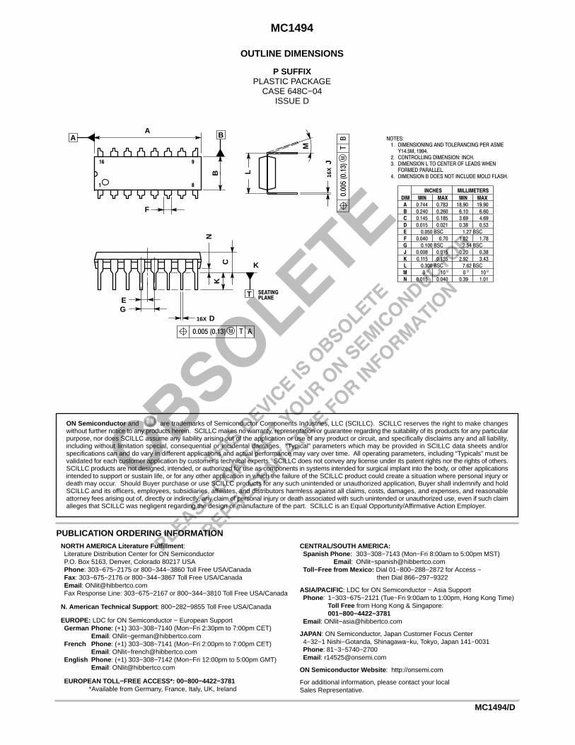
P SUFFIXPLASTIC PACKAGE
CASE 648C−04ISSUE D
OUTLINE DIMENSIONS
K
DIM MIN MAX MIN MAX
MILLIMETERSINCHES
A 0.744 0.783 18.90 19.90B 0.240 0.260 6.10 6.60C 0.145 0.185 3.69 4.69D 0.015 0.021 0.38 0.53E 0.050 BSC 1.27 BSCF 0.040 0.70 1.02 1.78G 0.100 BSC 2.54 BSCJ 0.008 0.015 0.20 0.38K 0.115 0.135 2.92 3.43L 0.300 BSC 7.62 BSCM 0 10 0 10 N 0.015 0.040 0.39 1.01
NOTES:1. DIMENSIONING AND TOLERANCING PER ASME
Y14.5M, 1994.2. CONTROLLING DIMENSION: INCH.3. DIMENSION L TO CENTER OF LEADS WHEN
FORMED PARALLEL.4. DIMENSION B DOES NOT INCLUDE MOLD FLASH.
16 9
1 8
DGE
NK
C
16X
AM0.005 (0.13) T
SEATINGPLANE
BM
0.00
5 (0
.13)
T
J16
X
M
L
AA
BF
T
B
ON Semiconductor and are trademarks of Semiconductor Components Industries, LLC (SCILLC). SCILLC reserves the right to make changeswithout further notice to any products herein. SCILLC makes no warranty, representation or guarantee regarding the suitability of its products for any particularpurpose, nor does SCILLC assume any liability arising out of the application or use of any product or circuit, and specifically disclaims any and all liability,including without limitation special, consequential or incidental damages. “Typical” parameters which may be provided in SCILLC data sheets and/orspecifications can and do vary in different applications and actual performance may vary over time. All operating parameters, including “Typicals” must bevalidated for each customer application by customer’s technical experts. SCILLC does not convey any license under its patent rights nor the rights of others.SCILLC products are not designed, intended, or authorized for use as components in systems intended for surgical implant into the body, or other applicationsintended to support or sustain life, or for any other application in which the failure of the SCILLC product could create a situation where personal injury ordeath may occur. Should Buyer purchase or use SCILLC products for any such unintended or unauthorized application, Buyer shall indemnify and holdSCILLC and its officers, employees, subsidiaries, affiliates, and distributors harmless against all claims, costs, damages, and expenses, and reasonableattorney fees arising out of, directly or indirectly, any claim of personal injury or death associated with such unintended or unauthorized use, even if such claimalleges that SCILLC was negligent regarding the design or manufacture of the part. SCILLC is an Equal Opportunity/Affirmative Action Employer.
PUBLICATION ORDERING INFORMATIONCENTRAL/SOUTH AMERICA:Spanish Phone : 303−308−7143 (Mon−Fri 8:00am to 5:00pm MST)
Email : ONlit−[email protected]−Free from Mexico: Dial 01−800−288−2872 for Access −
then Dial 866−297−9322
ASIA/PACIFIC : LDC for ON Semiconductor − Asia SupportPhone : 1−303−675−2121 (Tue−Fri 9:00am to 1:00pm, Hong Kong Time)
Toll Free from Hong Kong & Singapore:001−800−4422−3781
Email : ONlit−[email protected]
JAPAN : ON Semiconductor, Japan Customer Focus Center4−32−1 Nishi−Gotanda, Shinagawa−ku, Tokyo, Japan 141−0031Phone : 81−3−5740−2700Email : [email protected]
ON Semiconductor Website : http://onsemi.com
For additional information, please contact your localSales Representative.
MC1494/D
NORTH AMERICA Literature Fulfillment :Literature Distribution Center for ON SemiconductorP.O. Box 5163, Denver, Colorado 80217 USAPhone : 303−675−2175 or 800−344−3860 Toll Free USA/CanadaFax: 303−675−2176 or 800−344−3867 Toll Free USA/CanadaEmail : [email protected] Response Line: 303−675−2167 or 800−344−3810 Toll Free USA/Canada
N. American Technical Support : 800−282−9855 Toll Free USA/Canada
EUROPE: LDC for ON Semiconductor − European SupportGerman Phone : (+1) 303−308−7140 (Mon−Fri 2:30pm to 7:00pm CET)
Email : ONlit−[email protected] Phone : (+1) 303−308−7141 (Mon−Fri 2:00pm to 7:00pm CET)
Email : ONlit−[email protected] Phone : (+1) 303−308−7142 (Mon−Fri 12:00pm to 5:00pm GMT)
Email : [email protected]
EUROPEAN TOLL−FREE ACCESS*: 00−800−4422−3781*Available from Germany, France, Italy, UK, Ireland