Embed Size (px)
Citation preview

1
Water-based and Biocompatible 2D Crystal Inks: from Ink Formulation to All- Inkjet Printed Heterostructures
D. McManus1, S. Vranic2, F. Withers3, V. Sanchez-Romaguera4, M. Macucci5, H. Yang1, R. Sorrentino1,
K. Parvez1, S. Son1, G. Iannaccone5, K. Kostarelos2, G. Fiori5, C. Casiraghi1*
1 School of Chemistry, University of Manchester, UK
2 Nanomedicine Lab, Faculty of Medical and Human Sciences, University of Manchester, UK
3 School of Physics and Astronomy, University of Manchester, UK
4 Manchester Enterprise Centre, Alliance Manchester Business School, University of Manchester, UK
5 Dipartimento di Ingegneria dell’Informazione, Universita’ di Pisa, Pisa, Italy
* Corresponding author email: [email protected]
Fully exploiting the properties of 2D crystals requires a mass production method able to
produce heterostructures of arbitrary complexity on any substrate, including plastic.
Solution processing of graphene allows simple and low-cost techniques such as inkjet
printing to be used for device fabrication. However, available inkjet printable
formulations are still far from ideal as they are either based on toxic solvents, have low
concentration, or require time-consuming and expensive formulation processing. In
addition, none of those formulations are suitable for thin-film heterostructure fabrication
due to the re-mixing of different 2D crystals, giving rise to uncontrolled interfaces, which
results in poor device performance and lack of reproducibility.
In this work we show a general formulation engineering approach to achieve highly
concentrated, and inkjet printable water-based 2D crystal formulations, which also
provides optimal film formation for multi-stack fabrication. We show examples of all-
inkjet printed heterostructures, such as large area arrays of photosensors on plastic and
paper and programmable logic memory devices, fully exploiting the design flexibility of
inkjet printing. Finally, dose-escalation cytotoxicity assays in vitro also confirm the inks
biocompatible character, revealing the possibility of extending use of such 2D crystal
formulations to drug delivery and biomedical applications.

2
The electronics industry has been dominated by metals and complementary metal-oxide-
semiconductor (CMOS) technology. However, constraints related to materials choice clearly appear
in transparent and flexible electronics, heat management and rapid customisation – all of which
present challenges to traditional fabrication methods. An important advance was obtained with the
introduction of conductive polymers,1 which allow simple, versatile, and low-cost techniques, such
as inkjet printing, to be used for manufacturing functional devices.2-4
The isolation of graphene5 has unveiled a wide range of novel 2-Dimensional (2D) materials with
outstanding properties.6-8 This new class of materials shows great promise for use in flexible
electronics because their atomic thickness allows for maximum electrostatic control, optical
transparency, sensitivity and mechanical flexibility.6,9 In addition, since 2D crystals are characterized
by out of plane Van der Waals interactions, they can be easily combined in one multi-layer stack,
offering unprecedented control of the properties and functionalities of the resulting
heterostructure-based device.10 In this framework, inkjet printing can provide a very attractive route
to low-cost and large-scale fabrication of heterostructures on any substrate. Furthermore, inkjet
printing allows fabrication of complex heterostructures, which can provide multiple functionalities
and improved performance.11 Methods such as vacuum filtration and spin/spray coating, which have
been previously used for heterostructure fabrication,12,13 offer poor control of thickness and
roughness of the layers, and have very limited design flexibility, in particular for fabrication of
complex heterostructures and arrays.
To make inkjet printing a suitable technique for fabrication of all-printed heterostructures, it is
necessary to carefully engineer 2D-crystal inks. Available inkjet printable formulations, produced by
Liquid-Phase Exfoliation (LPE),14 are still far from ideal as they are either based on toxic and
expensive solvents,15-17 or require time-consuming and expensive formulation processing,18-22
substrate functionalization17 or need relatively high temperature to dry,16,17 which limits the range of
substrates that can be used. In addition, none of those formulations are suitable for thin-film
heterostructure fabrication, which requires multi-stack formation with well defined interfaces. Fully
printing a multi-layer stack is a very well known challenge for printing technology3,23: the different
materials in the stack tend to re-disperse at the interface, producing uncontrolled interfaces,
(Supporting Information, e.g. Figure S2), resulting in poor device reproducibility and performance.
Better control of interfacial effects and processing conditions allowed significant improvements in
the performance of organic field effect transistors.24
Making new printable formulations of functional materials is very challenging: inkjet printing
requires the ink to have specific physical properties3,4; water, for example, is unsuitable for both

3
LPE14 and inkjet printing.4 Surfactants can be added to water to both lower the surface tension and
to stabilise the exfoliated nanosheets.25 Such inks are not ideal for printed electronics as they have a
low concentration of 2D crystals (<0.1 weight %)26 and contain a high amount of residual surfactant.
Other examples of printable water-based inks refer to graphene oxide (GO) or reduced-GO, which
are defective and require thermal or chemical treatments.
In this work we developed a simple method for the production of highly concentrated, stable, inkjet
printable, water-based inks that can be formulated for a range of 2D materials. No solvent exchange,
chemical treatment or harsh conditions are used. The ink composition has been optimized to
achieve optimal film formation for multi-stack formation, allowing fabrication of all-inkjet printed
heterostructures, such as arrays of all-printed photosensors over cm2 areas on plastic and
programmable logic devices completely made of 2D-crystals. Because the inks are expected to find
utility in several applications as different consumer products, we also investigated possible adverse
effects from exposure and determined their safety limitations by performing dose-escalation
cytotoxicity assays in vitro using lung and skin cells. Overall, no significant cytotoxic responses
compared to untreated cells were observed for all doses. Therefore, our inks could find important
applications also in drug delivery and biomedical applications.
Amongst steric and electrostatic stabilisers, pyrene sulfonic acid derivatives are able to produce
concentrated, stable (up to 1 year) water-based 2D crystal dispersions,27-29 characterized by a high
graphene to stabiliser ratio, compared to surfactants.30 This exfoliation method has been shown to
produce high quality (i.e. without oxygen-based groups) graphene dispersions.27 However, these
formulations are not inkjet printable (Figure S1-a in Supplementary Information). In order to be
printable, inks must have a viscosity (η), surface tension (γ) and density (ρ) within certain ranges for
a set nozzle diameter (α). The inverse Ohnesorge number is commonly used to predict if an ink will
form stable drops: .31 The ink will produce stable drops if 1 < Z < 14.31 For a nozzle
diameter of 21.5μm, Z is ≈ 40 for water. In order to lower Z, the surface tension must be reduced
and the viscosity increased using additives. Here triton x-100 was used to decrease the surface
tension from ≈73 mN m-1 to ≈40 mN m-1, while propylene glycol was used as co-solvent to increase
the viscosity from 1 mPa∙s to 1.37 mPa∙s. This also disrupts the weak Marangoni flow, which helps
reduce the coffee-ring effect.32 These values of surface tension and viscosity give Z ≈20 for the
modified water-based ink. Despite Z >14, the drop is stable, and no satellite drops or nozzle blocking
are observed (Video 1 in Supplementary Information). This is in agreement with water/ethylene
glycol inks,33 which can be printed with Z = 35.5 and N-Methyl-2-pyrrolidone (NMP)-based graphene
inks, which show good printability with Z > 20.16,17

4
Note also that the concentration of surfactant is a very important parameter, which needs to be
carefully optimized (Supplementary Information, Section 1). Surfactant and co-solvent can be added
before or after exfoliation of the bulk crystal. In this work we modify the dispersion after exfoliation;
note that we have never observed changes in concentration and stability (i.e. re-aggregation),
therefore the formulation modification does not alter the thickness distribution and quality of the
flakes, as also confirmed by electrical measurements. Triton x-100, a non-ionic surfactant, was
chosen on purpose to avoid disrupting the electrostatic stabilization of graphene flakes provided by
pyrene sulfonic acid derivatives.
Figure 1a shows an optical picture of the inks. Several 2D materials have been successfully exfoliated
and printed, including graphene, MoS2, WS2 and h-BN. Figure 1 b and c show some examples of
printed patterns obtained with water-based graphene and MoS2 inks, respectively, on PEL P60
paper. Other examples can be found in the Supplementary Information, Figure S7. We point out that
no treatment of the substrate is used and the whole printing process is performed under ambient
Figure 1 | Range of inkjet printable inks and their properties. a, Optical Image of water-based 2D-crystal
inks. b, Nobel medal printed with water-based graphene ink on paper PEL 60 c, Printed “MoS2” logo with
water-based MoS2 ink on paper PEL 60 with increasing number of printed passes (from 1 to 4, moving from
top to bottom). Note the relatively good contrast with the paper obtained already with one printed pass. d,
Optical picture of an array of all-printed Gr/WS2/Gr heterostructures on PET. e, Sheet resistance as a function
of the thickness of graphene lines (1 cm length) printed on silicon (Si/SiO2), before and after annealing. Ink
concentration ≈ 2 mg/mL. The data is compared with the sheet resistance reported for NMP-based graphene
inks from Ref. 17. f, Sheet resistance for increasing number of printed passes for graphene lines (2 cm length)
printed on paper PEL 60 (inset shows the optical pictures of the printed lines made with 1, 5, 10, 15 and 20
printed passes, from bottom to top) with drop spacing of 40 μm (red points). Note that in the case of paper,
its porosity allows printing with small drop spacing (25 μm), leading to deposition of larger amount of
material per unit area with fewer printing passes, eventually minimizing Rs (blue points). Ink concentration ≈ 3
mg/mL.

5
conditions. Figure 1 e and f show the values of sheet resistance Rs of printed graphene lines on
silicon (Si/SiO2) and paper, respectively, for increasing number of printed passes: Rs is infinite before
the percolation threshold is reached,34 after which Rs decreases rapidly until the percolation to bulk
threshold transition, at which point the graphene behaves like a bulk material, with only small
changes in sheet resistance resulting from each subsequent printing pass. Rs values range between
≈10 MΩ/□ and ≈1 kΩ/□, which are comparable with literature results obtained for other types of
printable graphene inks.16,17,19,35 Figure 1e compares Rs values obtained with our water-based inks
and NMP-based graphene inks printed on untreated silicon (Si/SiO2).17 Note that thermal annealing
at 300°C for 1h under nitrogen atmosphere can be used to further lower Rs, Figure 1e, but this
process can be used only for some substrates, such as silicon (Si/SiO2), quartz, and polyimide. Note
that the thickness of the printed line varies as a function of ink concentration. In figure 1(e), an ink
with concentration of 2 mg/mL was used, giving rise to a thickness of ≈5 nm per printing pass on
silicon (Si/SiO2). In the case of paper, its porosity allows fast drying and therefore printing with
reduced drop spacing. By optimizing the drop spacing for a fixed ink concentration (2-3 mg/mL), we
have been able to obtain Rs below 1KΩ/sq above 40 printing passes (blue points, Figure 1(f)). The
thickness per pass on paper cannot be measured accurately due to the roughness of the substrate.
The basic ink formulation process can be further improved by removing excess pyrene after
exfoliation with the use of a washing step. This allows us to increase graphene concentration up to 8
mg/mL (0.8 w%), enabling graphene conductive lines to be printed with just one printing pass. This is
highly favourable for inkjet printing as a single pass printing allows reducing fabrication time and
costs. This is visible also in figure 1c, where just one printed pass gives rise to a noticeable colour
contrast of the MoS2 pattern to the paper.
In printing technology it is common to modify a formulation to enhance some of its properties (such
as conductivity, mechanical integrity and adhesion to the substrate).3 In order to print a
heterostructure, i.e. a multi-layer stack, a binder was also added to the printable ink to minimize the
re-dispersion at the interface. The type and amount of binder depends on many factors including the
concentration, solvent and stability of the ink.36 In our case, we selected polysaccharide Xanthan
gum (XG) because it is soluble in water and provides the dual benefits of acting as a binder and
requiring a low concentration to increase the viscosity. This allows retention of the inks electrical
properties. The addition of the binder produces inks with non-Newtonian viscosity, i.e. an ink with
shear-thinning properties, which helps form uniform lines as the viscosity increases substantially
after the droplets are deposited on the surface. A major advantage of XG over other binders is its
biocompatibility.37 Note that a change in the ink chemistry is known to affect the stability and

6
printability of the ink; in our case, the binder gives rise to a small filament (tail) on ejection of the ink
from the nozzle which re-joins with the main drop without forming a satellite drop, so the ink is still
printable (Supplementary Information, Figure S8). Note that the binder can be added only after
exfoliation as the high shear forces involved in exfoliation cause polymer degradation.38
With this modified water-based ink we fabricated a heterostructure-based photodetector onto
Si/SiO2 by printing a first graphene line of ≈50 nm thickness at 50 °C. This acts as bottom graphene
electrode (GrB). A WS2 square of ≈100 nm thickness, acting as photo-active element, was then
printed across the graphene line and finally a second graphene line (≈50 nm thickness) was printed
perpendicularly to the first, acting as top graphene electrode (GrT). The schematic of the
GrB/WS2/GrT heterostructure is shown in Figure 2a. Figure 2b (left panel) shows an optical picture of
an array of 16 heterostructures on an area of 1 cm x 1 cm on silicon (Si/SiO2). Figure 2b (right panel)
shows a high magnification optical picture of one of the heterostructures. Note the typical
Figure 2 | Fully inkjet printed heterostructures on Si/SiO2. a, Schematic of an all-printed GrB/WS2/GrT
heterostructure on Si/SiO2 substrate. b, (left panel) Optical picture of an array of 4 x 4 GrB/WS2/GrT
heterostructures printed on Si/SiO2; (right panel) Optical picture of one of the heterostructures, showing the
two graphene electrodes and the square of photo-active material; c, Raman map measured on the red dotted
square in b (right panel) showing the intensity of the 2D peak and the A1g peak (d). e, I-Vb curves measured
under different laser power (at 488nm); f, photo-current measured at Vb = 200 mV as a function of the laser
power; inset, photo-current map measured on the white dotted square in b, right panel. The red dotted line is a
guide for the eyes.

7
interference colours, which are already an indication of multiple-stack formation. Raman mapping at
488 nm excitation wavelength was performed on the dotted red square (≈500 μm x 500 μm) in
Figure 2b (right panel). Figure 2 c and d show the Raman maps of the intensity of the 2D peak of
graphene and the A1g peak of WS2, respectively. This figure shows that the material has been
deposited uniformly. The Raman spectra show the typical features of liquid-phase exfoliated
graphene and WS2 (Supplementary Information, Figure S9). After printing was completed, the
sample was annealed under N2 atmosphere at 300°C for 1 hour to remove residual moisture. The
non-linear I-V curve, Figure 2e, confirms that multi-stacking layers were formed, with no bias voltage
required for photocurrent response (Supplementary Information, Section 4). Photocurrent mapping,
inset Figure 2f, shows uniform photocurrent response in the overlap region between the two
graphene electrodes and the WS2 square. The photo-current efficiency of the printed devices is
comparable with other heterostructures fabricated from inks using non-scalable methods.12 Figure
2f also shows a power law for photocurrent vs laser power, which breaks at laser powers above ≈0.5
mW. We found that all of the 16 heterostructures show the same I-V characteristic, within the
experimental error (further data are included in the Supplementary Information, Section 4).
Therefore, device fabrication yield on silicon (Si/SiO2) is found to be 100 %.
As inkjet printing is extremely attractive for fabrication on flexible substrates, an array of 20
GrB/WS2/GrT heterostructures were printed onto PET film on an area of 3 cm x 4 cm with no
annealing performed, Figure 1d. The I-V curves in Figure 3a show non-ohmic behaviour under no or
little illumination, with the similar power law observed for the device in Figure 2. Figure 3b shows
that no photo-current saturation is reached for laser powers up to ~3 mW (higher powers cause
substrate degradation), in contrast to the device in Figure 2. This is due to the thicker GrT used in the
case of PET substrate, which decreases the effective laser power reaching WS2 . Bending test shows
that photocurrent is stable up to ~2 % strain (Figure 3c), in agreement with previous results reported
for heterostructures made by inks.12 Note that at higher strain, the silver contacts break down. It is
also interesting to compare the conductivity of the devices in Figure 2 and 3a: the out-of-plane
resistance is 3.8 MΩ at 1V for the device in Figure 2, although the exact value depends on the
voltage at which the current is measured due to the non-linearity of the I-V curve (see also Figure
4e). The in-plane resistances range from 250kΩ for GrB to 600 kΩ for GrT: the larger resistance of GrT
is likely due to the more uneven surface on which the top contact is printed (i.e., on top of GrB and
WS2). Both values include contact resistance (~ 10 kΩ). For the device in Figure 3a, the out-of-plane
resistance is 13 MΩ at 0.5 V. Figure S14 shows the narrow distribution of out-of-plane conductivities
for an array of heterostructures printed on glass.

8
We remark that several strategies can be used for improving the device performance. For example
GrB or GrT can be replaced by Chemical Vapour Deposited (CVD) graphene, lowering the total
resistance and increasing the optical transparency of the heterostructure. Figure S12 in the
Supplementary Information shows WS2 printed onto CVD graphene on silicon (Si/SiO2): the inks form
uniform patterns on the CVD graphene, no coffee ring or re-dispersion is observed, showing that
inkjet printing and CVD technologies are perfectly compatible. A simple way to improve the device
performance is to reduce the graphene electrode resistance. This can be easily obtained by
maximizing the amount of material printed per unit area, either by increasing the ink concentration
or by increasing the number of passes (see GrB/MoS2/GrT heterostructure, Section 4 in the
Supplementary Information). In the case of porous substrates, such as paper, the solvent absorption
allows minimizing the drop spacing during printing, which in turn increases the amount of material
printed per unit area (Figure 1 f, blue points). Following this strategy, we fabricated a GrB/WS2/GrT
Figure 3 | Flexible heterostructures fully printed onto plastic and paper. a, I-Vb curves of an all-printed
GrB/WS2/GrT heterostructures on PET as a function of increasing laser power. (λ = 514 nm) b, photo-current
measured at Vb = 0.5 V and λ = 514 nm as a function of increasing laser power (the red line is an exponential fit
of the experimental data). c, Bending test showing that the photo-current of an all-printed GrB/WS2/GrT
heterostructures on PET is stable up to ~2% strain. d, I-Vb curves of an all-printed GrB/WS2/GrT heterostructures
on paper as a function of increasing laser power (λ = 514 nm). e, photo-current measured at Vb = 0.5 V and λ =
514 nm as a function of increasing laser power (the red line is an exponential fit of the experimental data).
Inset: zoom on the data for Vb between -0.07 V and 0.07 V to show the changes in the short-circuit current with
the laser power. f, Current generated by switching on and off the laser source and under Vb = 1 V.
Photoresponsivity higher than 1 mA/W is obtained.

9
photodetector on paper by printing a graphene ink with concentration of 2 mg/mL and using ~25 μm
drop spacing, and 20 printing passes (Figure S15 in the SI). Figure 3 d shows the I-Vb curves of the
photosensor: the resistance decreases with increasing laser power. Figure 3 e shows the photo-
current measured at Vb = 0.5 V and λ = 514 nm as a function of increasing laser power. Figure 3 f
shows the current generated by switching on and off the laser every 10 seconds at Vb of 1V. There is
1 order of magnitude increase in current, when switching from off to on, giving rise to responsivity
higher than 1 mA/W, well above the typical resonsivity reported for devices made with liquid-phase
exfoliated 2D crystals.12,16 Note that for our devices a higher laser power can be used due to the
increased thickness of the top graphene electrode.
On the other hand, the ability to design heterostructures and to make arrays by inkjet printing can
be exploited to make novel devices. Here we show for the first time programmable logic memory
devices, made completely with 2D crystals. Information storage is essential in any data processing
system. As a consequence, while pursuing the goal of obtaining an “all inkjet” printed circuit, we
have to necessarily address the issue of implementing such an important building block.
To this purpose, we propose a programmable logic memory device, enabled by the ink-jet printing
technology, in which programming is performed at the time of fabrication. A “word” is stored in the
memory through the definition of a horizontal stripe (“word-line”) and vertical stripes, one for each
bit of the word (which will be referred to as “bit-lines"), all of them made of graphene (Fig. 4a). A
logic “1” is stored by short-circuiting the bit line to the word line, while a logic “0” is encoded by
including a semiconducting layer (i.e., WS2), between the word line and the corresponding bit line,
which eventually suppresses the current. In Fig. 4b, we show the fabricated device, including the
schematic of the complete circuit set up for the measurements, with the external bias voltage source
Vp and the load resistors RL. In particular, when a voltage is applied to the word line (i.e., 0.5 V), the
stored word is read in terms of the voltage VBi across each pull-down resistor RL, with higher voltage
values (greater than 0.35 V) interpreted as logic “1” and lower voltage values (less than 0.135 V) as
logic “0” (black solid line in Fig. 4c): in this specific case, the device is programmed with the word
“010010001”. We have also performed circuit simulations, considering a distributed resistance for
the graphene word and bit lines, and assuming that the graphene/WS2/graphene junction (logic “0”)
behaves as an ambipolar device. In particular, the I-V characteristics have been extracted from the
measurement performed on the circuit in Fig. 4a, and included into the SPICE circuit simulator (in
Fig. 4e we show an I-V characteristic of a junction as well as that of a short-circuit). Simulation
results of the equivalent circuit of Fig. 4a (i.e., Fig. 4d) are shown in Fig. 4c (red dashed lines),
showing good agreement between experimental and theoretical results.

10
The proposed device represents the first attempt to fabricate a memory with inkjet technology
based on 2D materials and it can be exploited in a wide range of applications. As an example, it could
be included in printed RF product tags, in order to store an identification number. Note that the
inclusion of additional elements in the device, such as diodes and transistors, would allow the device
to perform more complex functions and to increase the size of the read-only memory up to values of
practical interest.
Finally, the potential adoption of 2D-crystal inks in displays, smart packaging and textiles, printed
biological, chemical and environmental sensors as well as energy devices, requires early
determination of the risk associated with exposure of living organisms. Furthermore, graphene is a
remarkable material for biomedical applications.39 To offer an initial indication of the
biocompatibility profile of these water-based inks, we conducted a series of cytotoxicity studies. We
studied the response to dose-escalated ink exposure using cell culture models representative of the
human tissues that constitute the primary physiological barriers in non-occupational (e.g. skin
exposure of consumers) and occupational (e.g. pulmonary exposure of workers production lines of
Figure 4 | Logic memory device. a, Sketch of the fabricated device – The Programmable Read Only Memory
(PROM) is composed of a horizontal (word line) and vertical lines (bit lines) made of ink-jet graphene. A logic
“1” is stored at regular intersections of the word line and the bit line, while a logic “0” is programmed by
printing WS2 between the two. The sketch shows a 4-bit memory storing the word “1010”. b, Micrograph
picture of the fabricated device, where the bias voltage (Vp) source and load resistors are added. c,
Experimental (black solid line) and simulated results (red dashed line) for the operation of the circuit in a). d,
Schematic of the equivalent electronic circuit. e, I-V characteristics of a graphene/WS2/graphene junction and
of a short-circuit.

11
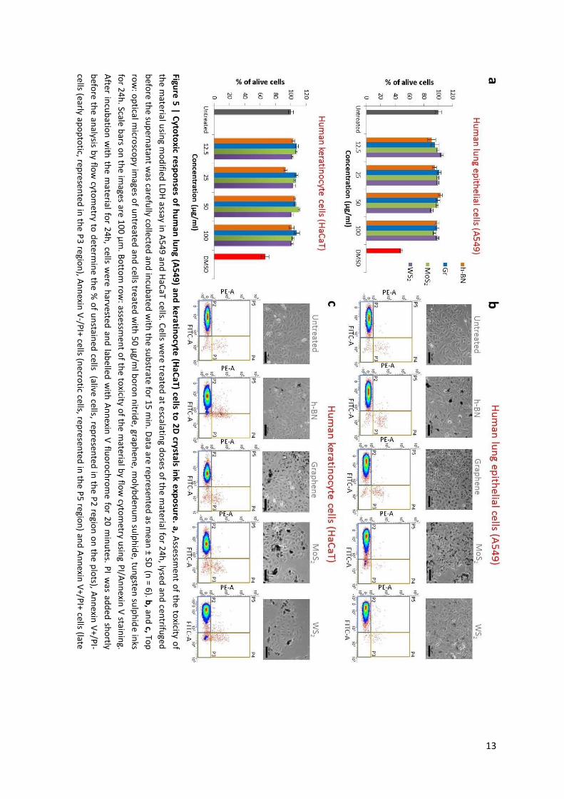
such materials) scenarios. The viability of human lung (human alveolar epithelial cells; A549) and
skin (human keratinocytes; HaCaT) cells was assessed using two assays: the modified LDH assay – a
colorimetric assay used to evaluate cellular membrane damage induced by the material; and
PI/Annexin V staining used to distinguish cell viability by flow cytometry (FACS).
The modified LDH assay was developed40 to avoid potential interferences that are often reported as
a result of interfering interactions between nanomaterials and reagents in colorimetric assays.41 No
differences in cell survival after 24hr of treatment with increased doses of the 2D inks were
observed compared to untreated cells (Figure 5a). The LDH assay data was validated using FACS
(Figure 5b and c) by staining with cellular markers of apoptosis (Annexin V) and necrosis (Propidium
Iodide). Cells exhibiting different responses to 2D ink exposure were gated according to: healthy
(unlabeled) cells (P2), early apoptotic (P3), late apoptotic and/or necrotic (P4) and necrotic cells (P5).
Even at the highest dose of 100 µg/mL, cells appeared unstained, indicating the presence of
predominantly alive cells (more than 90% of counted cells appeared in this region; Supplementary
Information, Figure S16). Overall, no significant cytotoxic responses compared to untreated cells
were observed for all doses (Supplementary Information, Figure S17). Optical microscopy of the 2D
ink-treated cell cultures (50 µg/mL for 24 h, Figure 5 b and c) indicated strong interactions between
the material and the cells that can lead to binding and internalization, to be further investigated in
future studies. In the present work, no significant morphological changes indicative of cell death,
such as decreased cellular confluence compared to the untreated cells; loss of cell/cell contact
between neighbouring cells; contracted nuclei or multinucleated giant cells, were observed after
treatment. Overall, the modified LDH, FACS and microscopy data all corroborated to indicate that
the 2D material used did not induce any significant cytotoxic responses in the two cell lines and the
dose-escalation regime studied here.
We remark that, to date, there have been very limited studies investigating the cytotoxic responses
from exposure to exfoliated 2D materials that can inform about any biocompatibility limitations. The
in vitro cytotoxic responses to MoS2 nanosheets, using different exfoliating agents to the ones used
in this study42-44 have reported no significant adverse response using different cell lines (PC12, rat
pheochromocytoma cells; Beas2B, human epithelial lung cells; THP-1, human myeloid cell line). In
another study the cytotoxic responses of A549 cells using different lithium-based exfoliating agents
have been reported.45 Similarly, cytotoxic responses in HeLa (human cervical cancer cell line), 4T1
(mouse breast cancer cell line) and 293T (human embryonic kidney) cells to WS2 nanosheets
indicated that the type of exfoliating agent and their surface modifications play a critical role in the
induced cytotoxicity.46,47 In order to determine the biocompatibility profile of exfoliated 2D

12
nanosheets thoroughly, more systematic studies should be performed, accounting for the
anticipated route and dose of exposure and employing more complex models to determine potential
adverse reactions. Here, we provided an initial comparative study between four types of 2D inks and
two human cell lines that indicated biocompatibility within the dose escalation studied.
In conclusion, we have produced water-based, inkjet printable, and biocompatible 2D crystal inks
that can provide new paradigms for manufacturing of fully printed 2D-crystal based devices of
arbitrary complexity, which can be exploited in a wide range of applications. Due to the simplicity,
and low cost of device fabrication and integration, we envisage this technology to find potential in
smart packaging applications and labels, in particular for food, drinks, pharmaceuticals and
consumer goods, where thinner, lighter and cheaper and easy to integrate components are needed.
13
Figure
5 | C
ytoto
xic resp
on
ses o
f hu
man
lun
g (A5
49
) and
kera
tino
cyte (H
aCaT) ce
lls to 2
D crystals in
k exp
osu
re. a, A
ssessmen
t of th
e toxicity o
f
the m
aterial usin
g mo
dified
LDH
assay in A
54
9 an
d H
aCaT
cells. Cells w
ere treated at e
scalating d
oses o
f the m
aterial for 2
4h
, lysed an
d cen
trifuge
d
befo
re the su
pern
atant w
as carefully co
llected an
d in
cub
ated w
ith th
e sub
strate for 1
5 m
in. D
ata are represen
ted as m
ean ± SD
(n = 6
). b, an
d c, To
p
row
: op
tical micro
scop
y images o
f un
treated an
d cells treated
with
50
µg/m
l bo
ron
nitrid
e, graph
ene, m
olyb
den
um
sulp
hid
e, tun
gsten su
lph
ide in
ks
for 2
4h
. Scale bars o
n th
e images are 1
00
µm
. Bo
ttom
row
: assessmen
t of th
e toxicity o
f the m
aterial by flo
w cyto
metry u
sing
PI/A
nn
exin V
stainin
g.
After in
cub
ation
with
the m
aterial for 2
4h
, cells were h
arvested an
d lab
elled w
ith A
nn
exin V
fluo
roch
rom
e for 2
0 m
inu
tes. PI w
as add
ed sh
ortly
befo
re the an
alysis by flo
w cyto
metry to
determ
ine th
e % o
f un
stained
cells (alive cells, represen
ted in
the P
2 regio
n o
n th
e plo
ts), An
nexin
V+/P
I-
cells (early apo
pto
tic, repre
sen
ted in
the P
3 re
gion
), An
nexin
V-/P
I+ cells (necro
tic cells, represen
ted in
the P
5 regio
n) an
d A
nn
exin V
+/PI+ cells (late
apo
pto
tic and
/or n
ecrotic cells, sh
ow
n in
the P
4 regio
n). D
ata represen
ted as m
ean ± SD
(n = 3
).

14
Methods
Ink Preparation. Graphite (99.5% Grade) was purchased from Graphexel Ltd. All co-solvents, Triton
x-100 and Xanthan gum were purchased from Sigma-Aldrich, UK. 10 μL Dimatix cartridges and PEL
P60 paper were purchased from Printed Electronics Ltd. Si/SiO2 wafers were obtained from IDB
Technologies Ltd. CVD graphene was purchased from 2D-Tech Ltd. The dispersion was sonicated at
300W using a Hilsonic bath sonicator for 72 h. Flakes of the appropriate lateral size were collected
via differential centrifugation to reduce the chance of nozzle blockages. The liquid obtained was
centrifuged using a Sigma 1-14k refrigerated centrifuge at 903 g for 20 minutes before collecting the
supernatant. The collected supernatant was then centrifuged at 16600 g for 1 hour and the
precipitate re-dispersed in the printing solvent. The solvent consisted of less than 1:10 propylene
glycol:water by mass, ≥0.06 mg / mL triton x-100 and ≥0.1 mg/mL XG. The concentration of 2D
material was determined by UV-Vis spectroscopy, and the rheological properties were studied
before printing (Supplementary Information, Sections 1 and 2). The lateral size of the nanosheets
have been characterized by Atomic force Microscopy (Supplementary Information, Figure S5). No
aggregation is observed when transferred in the cartridge or during printing. More details are
provided in the Supplementary information.
Printing. We used a Dimatix DMP-2800 inkjet printer (Fujifilm Dimatix, Inc., Santa Clara, USA), which
can create and define patterns over an area of about 200 x 300 mm and handle substrates up to 25
mm thick. A waveform editor and a drop-watch camera system allows manipulation of the electronic
pulses to the piezo jetting device for optimization of the drop characteristics as it is ejected from the
nozzle. The nozzle plate consists of a single raw of 16 nozzles of 23 μm diameter spaced 254 μm with
typical drop size of 10 pL. Inks are printed onto a variety of substrates, in particular Silicon/SiO2 (290
nm thermally grown oxide layer), SiO2 (Quartz), PEL 60 paper (from Printed Electronics) and CVD
graphene (from 2DTech). The printed features have been characterized by optical microscopy,
Raman Spectroscopy, and Atomic Force Microscopy (Supplementary information, Section 3). Sheet
Resistance has been measured with 2 contact probes, so the values include contact resistance.
Photocurrent measurements. Photocurrent maps were collected using a WiTEC Alpha 300 confocal
Raman Microscope with 488 nm, 514.5 nm and 633 nm excitation wavelengths. Laser power was
measured by a Thorlabs PM100D optical power meter. A bias voltage was applied using a Keithley
2614B Sourcemeter, also used to record I-V curves of the photoactive elements. The optically
induced voltage change was measured across a 1 kΩ resistor by a Keithley 2182A Voltmeter and
relayed into the WiTEC control software to generate a photocurrent map. National Instruments
LabVIEW 2015 was used to control the sourcemeter and record data.

15
Cell Culture. Epithelial lung carcinoma cells (A549, ATCC, CCL-185) were maintained and passaged in
Nutrient Mix F12 Ham media (Sigma-Aldrich, UK) supplemented with 10 % FBS (Thermo Scientific,
UK), 50 μg/mL Penicillin, 50 μg/mL Streptomycin (Sigma-Aldrich, UK) at 37 °C in 5% CO2. Cells were
passaged twice a week using Trypsin-EDTA 0.05 % (Sigma-Aldrich, UK) when reached 80 %
confluence. Activity of trypsin was stopped using 10 % FBS. Human keratinocyte cells (HaCaT) were
generously provided by Dr Suzanne Pilkington (Dermatological Sciences, Institute of Inflammation
and Repair, University of Manchester) and were maintained in DMEM media (Sigma-Aldrich, UK)
supplemented with 10 % FBS, 50 μg/mL Penicillin, 50 μg/mL Streptomycin at 37 °C in 5 % CO2. Cells
were passaged twice a week using Trypsin-EDTA 0.05 % at 80 % confluence. Activity of trypsin was
stopped using 10 % FBS.
Cell Culture treatment. Depending on the experiment, cells were seeded in 96 (LDH assay) or 12
(FACS analysis) well plates (Costar, Sigma) and treated when reached 70-80 % confluence. All
treatments were performed in the cell culture medium in the absence of FBS, 10 % FBS was added to
each well 4 h after the treatment. h-BN (1.6 mg/mL), Graphene (5.84 mg/mL), MoS2 (1.44 mg/mL)
and WS2 (0.5 mg/mL) were vortexed shortly before making final dilutions for the treatment in the
corresponding cell culture media. Cells were exposed to 12.5 - 25 - 50 - 100 μg/mL h-BN, Graphene,
MoS2 or WS2 material for 24 h. Solvent (containing 0.06 mg/mL Triton x-100) used to stabilize the
inks was also tested for its toxicity using the following concentrations: 0.012 – 0.006 – 0.003 –
0.0015 mg/ml Triton x-100 corresponding to the 100 – 50 – 25 – 12.5 µg/mL WS2 inks.
Annexin V-Alexa Fluor®488 conjugate/PI Assay. After 24 h of treatment at indicated concentrations,
supernatants were collected and cells were gently washed 3 times with PBS Ca2+/Mg2+ (Sigma-
Aldrich, UK). Annexin-V staining was performed according to the instructions of the manufacturer
(Thermo Fisher Scientific, UK). In brief, cells were trypsinized and merged with corresponding
supernatants, centrifuged at 1500 rpm for 5 min, then re-suspended in 100 μL Annexin binding
buffer (Thermo Fisher Scientific, UK) and stained with 2 μL Annexin V-Alexa Fluor®488 conjugate for
20 min at 15–25 °C. Propidium Iodide (1 mg/mL, Sigma) was added shortly before the analysis to the
final concentration of 1.5 μg/mL. 10 000 cells were analysed on a BD FACSVerseTM flow cytometer
using 488 nm excitation and 515 nm and 615 nm band pass filters for Annexin V and PI detection,
respectively. Electronic compensation of the instrument was performed to exclude overlapping of
the two emission spectra. Material alone was run in order to set up the gates including the cell
population for the analysis. Percentage of unstained, cells stained with Annexin V, PI or both was
calculated.

16
Modified LDH Assay. LDH assay was modified to avoid any interference coming from the
interactions of the material with assay.40 Briefly, the LDH content was assessed in intact cells that
survived the treatment, instead of detecting the amount of LDH released in the media upon
treatment. Media was aspirated and cells were lysed with 100 µL of lysis buffer for 45 min at 37 °C to
obtain cell lysate, which was then centrifuged at 4,000 rpm for 20 min in order to pellet down the
material. 50 µL of the supernatant of the cell lysate was mixed with 50 µL of LDH substrate mix
(Promega, UK) in a new 96-well plate and incubated for 15 min at room temperature, after which 50
μl stop solution was added.
(2)
The absorbance was read at 490 nm using a plate reader. The amount of LDH detected represented
the number of cells that survived the treatment. The percentage cell survival was calculated using
the equation above.
Acknowledgments
This work was partially supported by the Grand Challenge EPSRC grant EP/N010345/1, and the
European Science Foundation (ESF) under the EUROCORES Programme EuroGRAPHENE (GOSPEL).
F.W. acknowledges support from the Royal Academy of Engineering. DMM acknowledges the EPSRC
in the framework of the NoWNano CDT. SS acknowledges support by the Army Research Office. SV
would like to acknowledge the “RADDEL” project (Marie Curie Initial Training Network (ITN) grant
number 290023 under the EU´s FP7 PEOPLE program. KK, GI and GF would like to gratefully
acknowledge financial support from EU FP7-ICT-2013-FET-F GRAPHENE Flagship project (no.
604391). GI and GF gratefully acknowledge European Commission under Contract No. 696656
(Project ‘GRAPHENE FLAGSHIP’ Core 1). C.C. and D.M.M. acknowledge Kostya Novoselov, Steve
Yeates, Joe Wheeler, and Adam Valentine Parry for useful discussions.
Authors Contribution
C.C. conceived and directed the experiments. D.M.M. developed the inks with inputs from V.S.R.,
and conducted all experiments, after preliminary results that were obtained by H.Y. and R.S., under
the supervision of V.S.R and C.C. K.P. provided some electrical measurements on paper. S.S. did
transfer the CVD graphene. Electrical characterization of the devices was performed by F.W. and
D.M.M; G. F. conceived the logic memory device with inputs from C.C.; the device was fabricated by
D.M.M and measured by M.M. The toxicology study was performed by S.V. under the supervision of
K.K. The paper was written by C.C., D.M.M., G. F., S.V. and K.K. in close consultation with all authors.

17
Additional information
Competing financial interests: The authors declare no competing financial interests.
Supplementary Information contains additional details on the ink preparation and characterization
of the inks, nanosheets, printed films and devices. Additional details on the biocompatibility tests
and comparison with existing printable inks are also reported.
References
1 Salaneck, W. R., Lundstrom, I., Huang, W. S. & Macdiarmid, A. G. A 2-Dimensional Surface-State Diagram for Polyaniline. Synthetic Met 13, 291-297, doi:10.1016/0379-6779(86)90190-6 (1986).
2 Sirringhaus, H. et al. High-Resolution Inkjet Printing of All-Polymer Transistor Circuits. Science 290, 2123-2126 (2000).
3 Baeg, K.-J., Caironi, M. & Noh, Y.-Y. Toward Printed Integrated Circuits based on Unipolar or Ambipolar Polymer Semiconductors. Advanced Materials 25, 4210-4244, doi:10.1002/adma.201205361 (2013).
4 Hutchings, I. M. & Martin, G. D. Inkjet Technology for Digital Fabrication. (Wiley, 2012). 5 Novoselov, K. S. et al. Two-dimensional atomic crystals. Proceedings of the National
Academy of Sciences of the United States of America 102, 10451-10453, doi:10.1073/pnas.0502848102 (2005).
6 Novoselov, K. S. et al. A roadmap for graphene. Nature 490, 192-200 (2012). 7 Geim, A. K. Graphene: Status and Prospects. Science 324, 1530-1534,
doi:10.1126/science.1158877 (2009). 8 Geim, A. K. & Novoselov, K. S. The rise of graphene. Nat Mater 6, 183-191 (2007). 9 Akinwande, D., Petrone, N. & Hone, J. Two-dimensional flexible nanoelectronics. Nat
Commun 5, doi:10.1038/ncomms6678 (2014). 10 Geim, A. K. & Grigorieva, I. V. Van der Waals heterostructures. Nature 499, 419-425,
doi:10.1038/nature12385 (2013). 11 Withers, F. et al. Light-emitting diodes by band-structure engineering in van der Waals
heterostructures. Nat Mater 14, 301-306, doi:10.1038/nmat4205 (2015). 12 Withers, F. et al. Heterostructures Produced from Nanosheet-Based Inks. Nano Letters 14,
3987-3992, doi:10.1021/nl501355j (2014). 13 Kelly, A. G., Finn, D., Harvey, A., Hallam, T. & Coleman, J. N. All-printed capacitors from
graphene-BN-graphene nanosheet heterostructures. Applied Physics Letters 109, 023107, doi:doi:http://dx.doi.org/10.1063/1.4958858 (2016).
14 Hernandez, Y. et al. High-yield production of graphene by liquid-phase exfoliation of graphite. Nat Nano 3, 563-568, doi:10.1038/nnano.2008.215 (2008).
15 Coleman, J. N. et al. Two-Dimensional Nanosheets Produced by Liquid Exfoliation of Layered Materials. Science 331, 568-571, doi:10.1126/science.1194975 (2011).
16 Finn, D. J. et al. Inkjet deposition of liquid-exfoliated graphene and MoS2 nanosheets for printed device applications. Journal of Materials Chemistry C 2, 925-932, doi:10.1039/C3TC31993H (2014).
17 Torrisi, F. et al. Inkjet-Printed Graphene Electronics. ACS Nano 6, 2992-3006, doi:10.1021/nn2044609 (2012).
18 Li, J. et al. Efficient Inkjet Printing of Graphene. Advanced Materials 25, 3985-3992, doi:10.1002/adma.201300361 (2013).

18
19 Secor, E. B., Prabhumirashi, P. L., Puntambekar, K., Geier, M. L. & Hersam, M. C. Inkjet Printing of High Conductivity, Flexible Graphene Patterns. The Journal of Physical Chemistry Letters 4, 1347-1351, doi:10.1021/jz400644c (2013).
20 Yao, Y. et al. High-Concentration Aqueous Dispersions of MoS2. Advanced Functional Materials 23, 3577-3583, doi:10.1002/adfm.201201843 (2013).
21 Li, J., Naiini, M. M., Vaziri, S., Lemme, M. C. & Östling, M. Inkjet Printing of MoS2. Advanced Functional Materials 24, 6524-6531, doi:10.1002/adfm.201400984 (2014).
22 Zheng, J. et al. High yield exfoliation of two-dimensional chalcogenides using sodium naphthalenide. Nat Commun 5, doi:10.1038/ncomms3995 (2014).
23 Gorter, H. et al. Toward inkjet printing of small molecule organic light emitting diodes. Thin Solid Films 532, 11-15, doi:http://dx.doi.org/10.1016/j.tsf.2013.01.041 (2013).
24 Gaikwad, A. M. et al. Identifying orthogonal solvents for solution processed organic transistors. Organic Electronics 30, 18-29, doi:http://dx.doi.org/10.1016/j.orgel.2015.12.008 (2016).
25 Lotya, M. et al. Liquid Phase Production of Graphene by Exfoliation of Graphite in Surfactant/Water Solutions. J Am Chem Soc 131, 3611-3620, doi:10.1021/ja807449u (2009).
26 Lotya, M., King, P. J., Khan, U., De, S. & Coleman, J. N. High-Concentration, Surfactant-Stabilized Graphene Dispersions. ACS Nano 4, 3155-3162, doi:10.1021/nn1005304 (2010).
27 Yang, H. et al. A simple method for graphene production based on exfoliation of graphite in water using 1-pyrenesulfonic acid sodium salt. Carbon 53, 357-365, doi:10.1016/j.carbon.2012.11.022 (2013).
28 Yang, H. et al. Dielectric nanosheets made by liquid-phase exfoliation in water and their use in graphene-based electronics. 2D Materials 1, 011012 (2014).
29 Schlierf, A. et al. Nanoscale insight into the exfoliation mechanism of graphene with organic dyes: effect of charge, dipole and molecular structure. Nanoscale 5, 4205-4216, doi:10.1039/C3NR00258F (2013).
30 Parviz, D. et al. Dispersions of Non-Covalently Functionalized Graphene with Minimal Stabilizer. ACS Nano 6, 8857-8867, doi:10.1021/nn302784m (2012).
31 Reis, N. & Derby, B. Ink Jet Deposition of Ceramic Suspensions: Modeling and Experiments of Droplet Formation. MRS Online Proceedings Library Archive 625, doi:10.1557/PROC-625-117 (2000).
32 Hu, H. & Larson, R. G. Marangoni Effect Reverses Coffee-Ring Depositions. The Journal of Physical Chemistry B 110, 7090-7094, doi:10.1021/jp0609232 (2006).
33 Shin, P., Sung, J. & Lee, M. H. Control of droplet formation for low viscosity fluid by double waveforms applied to a piezoelectric inkjet nozzle. Microelectronics Reliability 51, 797-804, doi:http://dx.doi.org/10.1016/j.microrel.2010.11.017 (2011).
34 Stauffer, D. & Aharony, A. Introduction To Percolation Theory. (Taylor & Francis, 1994). 35 De, S. & Coleman, J. N. Are There Fundamental Limitations on the Sheet Resistance and
Transmittance of Thin Graphene Films? ACS Nano 4, 2713-2720, doi:10.1021/nn100343f (2010).
36 Secor, E. B. & Hersam, M. C. Emerging Carbon and Post-Carbon Nanomaterial Inks for Printed Electronics. The Journal of Physical Chemistry Letters 6, 620-626, doi:10.1021/jz502431r (2015).
37 Eastwood, M. A., Brydon, W. G. & Anderson, D. M. The dietary effects of xanthan gum in man. Food additives and contaminants 4, 17-26, doi:10.1080/02652038709373610 (1987).
38 Wheeler, J. S. R. et al. Effect of polymer branching on degradation during inkjet printing. Polymer Degradation and Stability 128, 1-7, doi:http://dx.doi.org/10.1016/j.polymdegradstab.2016.02.012 (2016).
39 Kostarelos, K. & Novoselov, K. S. Graphene devices for life. Nat Nanotechnol 9, 744-745, doi:10.1038/nnano.2014.224 (2014).

19
40 Ali-Boucetta, H., Al-Jamal, K. T. & Kostarelos, K. Cytotoxic assessment of carbon nanotube interaction with cell cultures. Methods Mol Biol 726, 299-312, doi:10.1007/978-1-61779-052-2_19 (2011).
41 Latiff, N. et al. Toxicity of layered semiconductor chalcogenides: beware of interferences. RSC Advances 5, 67485-67492, doi:10.1039/C5RA09404F (2015).
42 Shah, P., Narayanan, T. N., Li, C. Z. & Alwarappan, S. Probing the biocompatibility of MoS2 nanosheets by cytotoxicity assay and electrical impedance spectroscopy. Nanotechnology 26, 315102, doi:10.1088/0957-4484/26/31/315102 (2015).
43 Wang, X. et al. Differences in the Toxicological Potential of 2D versus Aggregated Molybdenum Disulfide in the Lung. Small 11, 5079-5087, doi:10.1002/smll.201500906 (2015).
44 Teo, W. Z., Chng, E. L., Sofer, Z. & Pumera, M. Cytotoxicity of exfoliated transition-metal dichalcogenides (MoS2 , WS2 , and WSe2 ) is lower than that of graphene and its analogues. Chemistry 20, 9627-9632, doi:10.1002/chem.201402680 (2014).
45 Chng, E. L., Sofer, Z. & Pumera, M. MoS₂ exhibits stronger toxicity with increased exfoliation. Nanoscale 6, 14412-14418, doi:10.1039/c4nr04907a (2014).
46 Yong, Y. et al. WS2 nanosheet as a new photosensitizer carrier for combined photodynamic and photothermal therapy of cancer cells. Nanoscale 6, 10394-10403, doi:10.1039/c4nr02453b (2014).
47 Cheng, L. et al. PEGylated WS(2) nanosheets as a multifunctional theranostic agent for in vivo dual-modal CT/photoacoustic imaging guided photothermal therapy. Adv Mater 26, 1886-1893, doi:10.1002/adma.201304497 (2014).