Embed Size (px)
DESCRIPTION
vlsi
Citation preview

Lecture 1. CMOS Logic
Dr. Zhaohui Wang Texas A&M University – Kingsville
EEEN 5333-001 Principles of VLSI Circuit Design Fall 2015
1

Introduction
• 1947, John Bardeen & Walter Brattain built he 1st funcitoning point contact transistor at Bell Lab.
• 1958, Jack Kilby, the 1st integrated circuit flip-flop with two transistors at Texas Instruments
• 2008, Intel’s Itanium microprocessor >2billion transistors,16Gb Flash memory>4billion transistors.
2
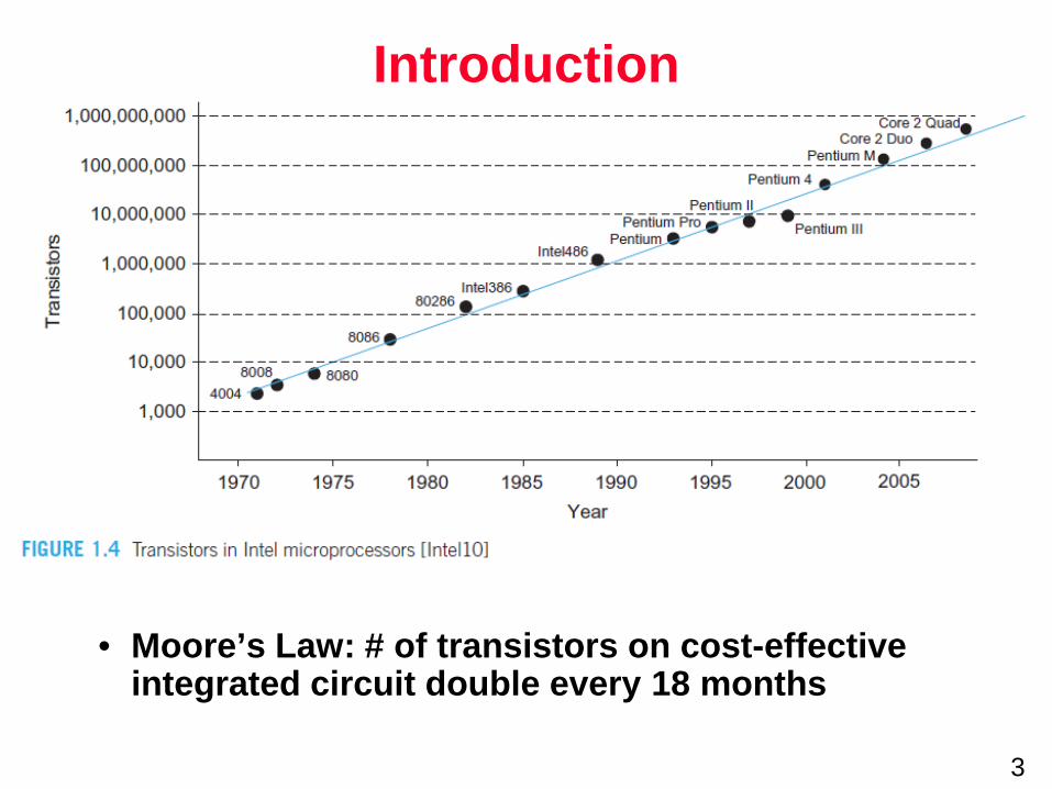
Introduction
• Moore’s Law: # of transistors on cost-effective integrated circuit double every 18 months
3

Introduction
• Dennard’s Scaling Law: as transistors shrink, they become faster, consume less power, and are cheaper to manufacture.
• The feature size of a CMOS manufacturing process refer to the minimum dimension of a transistor that can be reliably built.
• Dennard scaling has already begun to slow because transistors cannot be smaller than atom. By the 45nm generation, designer are having to make trade-off btw improving power and improving delay.
4

MOS Transistors
• Silicon (Si) – The basic starting material for most integrated circuits – Group IV element, forms covalent bonds with four
adjacent atoms – Pure silicon forms 3D lattice of atoms, cubic crystal – Conductivity can be raised by introducing small amount
impurities, called dopants, into silicon lattice.
5
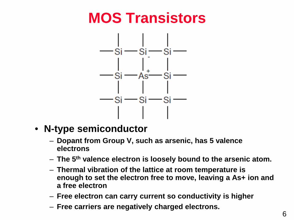
MOS Transistors
• N-type semiconductor – Dopant from Group V, such as arsenic, has 5 valence
electrons – The 5th valence electron is loosely bound to the arsenic atom. – Thermal vibration of the lattice at room temperature is
enough to set the electron free to move, leaving a As+ ion and a free electron
– Free electron can carry current so conductivity is higher – Free carriers are negatively charged electrons.
6

MOS Transistors
• P-type semiconductor – Dopant from Group III, such as boron, has 3 valence electrons – The dopant atom can borrow an electron from a neighboring
silicon atom, which in turn becomes short by one electron – That atom in turn can borrow an electron, and so forth, so the
missing electron, or hole, can propagate about the lattice. – The hole acts as a positive carrier
7

MOS Transistors
• Diode is a junction btw p-type and n-type silicon – Anode: p-type semiconductor – Cathode: n-type semiconductor – Vp>Vn, diode is forward biased and current flows. – Vp<Vn, diode is reverse biased and very little current flows.
8
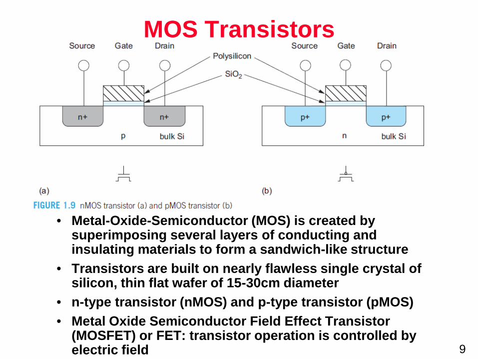
MOS Transistors
• Metal-Oxide-Semiconductor (MOS) is created by superimposing several layers of conducting and insulating materials to form a sandwich-like structure
• Transistors are built on nearly flawless single crystal of silicon, thin flat wafer of 15-30cm diameter
• n-type transistor (nMOS) and p-type transistor (pMOS) • Metal Oxide Semiconductor Field Effect Transistor
(MOSFET) or FET: transistor operation is controlled by electric field 9

• Transistor consists of a stack of conducting gate, an insulating layer of silicon dioxide, the silicon wafer (substrate, body, bulk).
• Gates of early transistor were metal • nMOS transistor is built with a p-type body and has regions of n-
type semiconductor adjacent to the gate called the source and drain. n+ indicates heavily doped n-type silicon
• pMOS transistor is built with a n-type body and has regions of p-type semiconductor adjacent to the gate called the source and drain. p+ indicates heavily doped p-type silicon
10
MOS Transistors

• nMOS: body is grounded – OFF: gate is grounded, p-n junction of source and drain to body
are reverse-biased junction. – ON: gate voltage is raised, creating electric field that attracts
free electrons to the underside of Si-SiO2 interface; voltage is high enough, electrons outnumber the holes, a thin region under the gate called channel is inverted to act as an n-type semiconductor →ON.
11
MOS Transistors

• pMOS: body is held at a positive voltage – OFF: gate is at a positive voltage, p-n junction of source and
drain to body are reverse-biased junction, not current flow. – ON: gate voltage is lowered, positive charges are attracted to
the underside of Si-SiO2 interface; a sufficiently low gate voltage invert channel and a conducting path of positive carrier is formed from source to drain.
12
MOS Transistors

MOS Transistors
• 1: or POWER, 5V →3V, 2.5V, 1.8V, …, 1.0V, ... • 0: or GROUND, 0V • nMOS: ON: g=1; OFF: g=0 • pMOS: ON: g=0; OFF: g=1
DDV
SSV
13

CMOS Logic
• Inverter • NAND Gate • CMOS Logic Gates • NOR Gate • Compound Gates • Tristates • Multiplexers • Sequential Circuits
– Latches – Flip-flops
14

CMOS Logic: Inverter
• COMOS Inverter or NOT gate use one nMOS transistor and one pMOS transistor
• A=0 →nMOS is OFF, pMOS is ON →Y is pulled up to ‘1’
• A=1 →nMOS is ON, pMOS is OFF →Y=0 15

CMOS Logic: NAND Gate
• K-input NAND gates are constructed using k series nMOS transistors (pull-down network) and k parallel pMOS transistors (pull-up network).
16
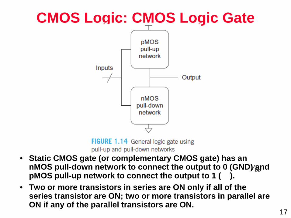
CMOS Logic: CMOS Logic Gate
• Static CMOS gate (or complementary CMOS gate) has an nMOS pull-down network to connect the output to 0 (GND) and pMOS pull-up network to connect the output to 1 ( ).
• Two or more transistors in series are ON only if all of the series transistor are ON; two or more transistors in parallel are ON if any of the parallel transistors are ON.
DDV
17
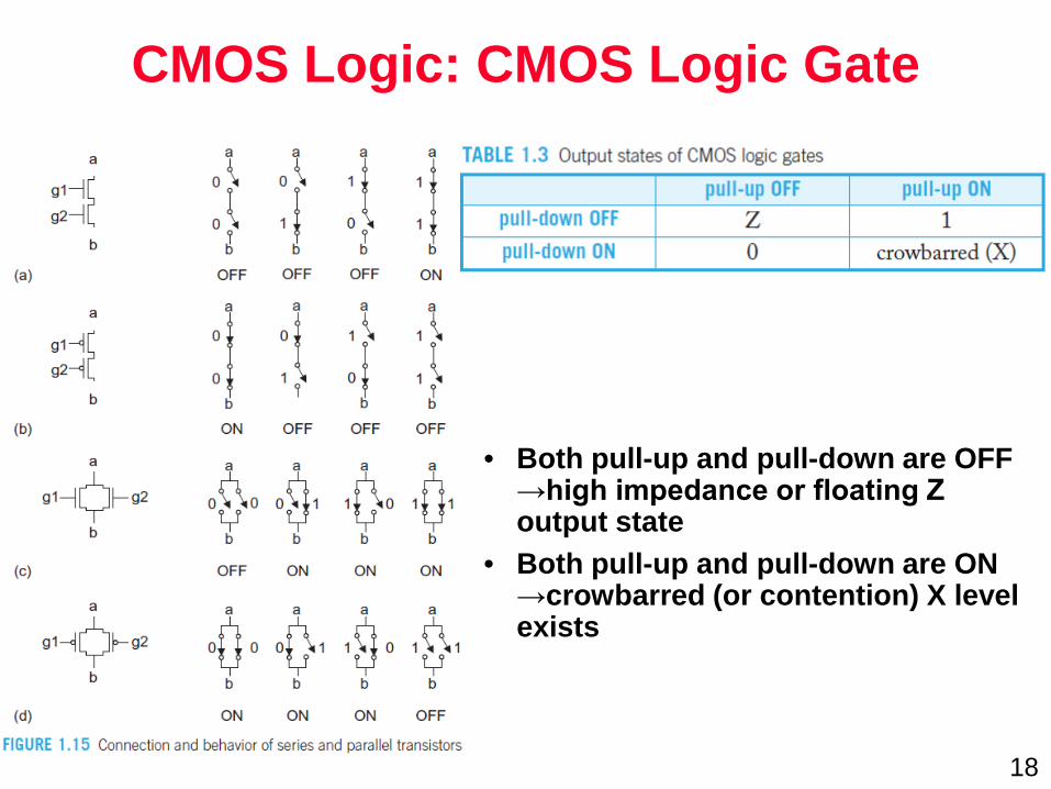
CMOS Logic: CMOS Logic Gate
• Both pull-up and pull-down are OFF →high impedance or floating Z output state
• Both pull-up and pull-down are ON →crowbarred (or contention) X level exists
18

CMOS Logic: NOR Gate
• The nMOS transistors are in parallel to pull the output low when either input is high.
• The pMOS transistors are in series to pull output high when both input are low.
• The output is never crowbarred or left floating. 19

CMOS Logic: NOR Gate
20

CMOS Logic: De Morgan's laws • De Morgan's laws
• Principles of conduction complements – Transistors that appear in series in the pull-down network
must appear in parallel in the pull-up network. – Transistors that appear in parallel in the pull-down
network must appear in series in the pull-up network.
BABA +=⋅
BABA ⋅=+
21
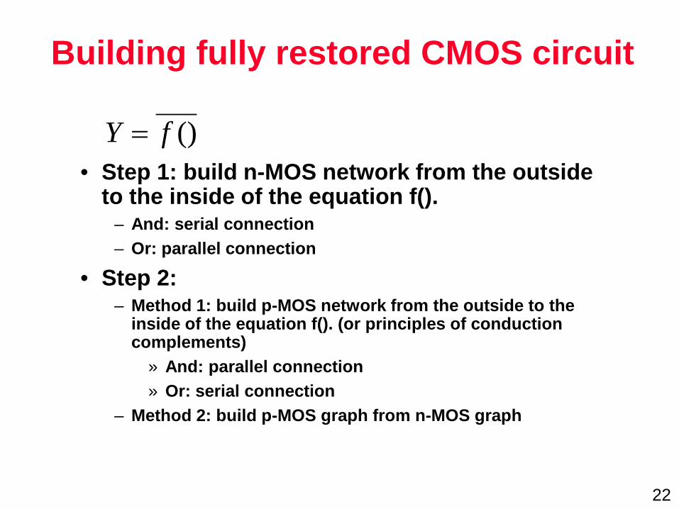
Building fully restored CMOS circuit
• Step 1: build n-MOS network from the outside
to the inside of the equation f(). – And: serial connection – Or: parallel connection
• Step 2: – Method 1: build p-MOS network from the outside to the
inside of the equation f(). (or principles of conduction complements)
» And: parallel connection » Or: serial connection
– Method 2: build p-MOS graph from n-MOS graph
22
()fY =

CMOS Logic: Compound Gate
• AND-OR-INVERT-22, or AOI22, can be used a 2-input multiplexer by connecting C=not A as select signal.
( ) ( )DCBA ⋅+⋅
( ) ( )DCBC ⋅+⋅ 23

CMOS Logic: Compound Gate
24

CMOS Logic: Pass Transistors
• The strength of signal is measured by how closely it approximates an ideal voltage source.
– nMOS transistor can pass strong 0 but degraded or weak 1 – pMOS transistor can pass strong 1 but degraded or weak 0
• Pass transistor – an nMOS or pMOS is used alone as an imperfect switch
25

CMOS Logic: Transmission Gates
• Transmission gate or pass gate – Combining an nMOS and a pMOS transistor in parallel – 0s and 1s are both passed in an acceptable fashion. – Double rail logic: both the control input and its complement are required
26

CMOS Logic: Fully restored logic gate
• Fully restored logic gate – The input drive the gate terminals of nMOS transistors in the pull-down network
and pMOS transistors in the complementary pull-up network – nMOS transistors only need to pass 0s and the pMOS only pass 1s, so the output
is always strongly driven and the levels are never degraded. – The design of static CMOS gates requires that they must be inverting
• Noninverting should be avoided – both nMOS and pMOS transistors produce degraded outputs. 27
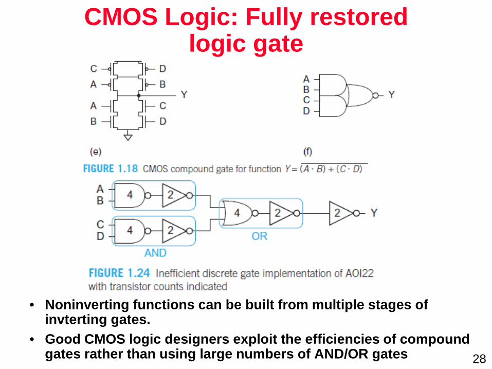
CMOS Logic: Fully restored logic gate
• Noninverting functions can be built from multiple stages of invterting gates.
• Good CMOS logic designers exploit the efficiencies of compound gates rather than using large numbers of AND/OR gates 28

CMOS Logic: Tristate & Transmission gate
• Transmission gate – has the same truth table as a tristate buffer. – It only requires two transistors but it is a nonrestoring circuit. – If the input is noisy or otherwise degraded, the output will receive the
same noise. – The delay of a series of nonrestoring gates increases rapidly with the
number of gates.
Tristate buffer Transmission gate
29
EN Y 1 Z 0 A

CMOS Logic: Tristate
• A restoring logic gate: the output is actively driven from or GND
• A tristate buffer can be built as an ordinary inverter followed by a tristate inverter.
• Multiplexer is preferred over tristate busses – If multiple units drive a common bus, contention occurs and power is wasted. – If no units drive the bus, it floats to invalid logic level, the receivers waste power. – Delay btw different enables switching can cause contention.
DDV
30
EN Y 1 Z 0 Ā

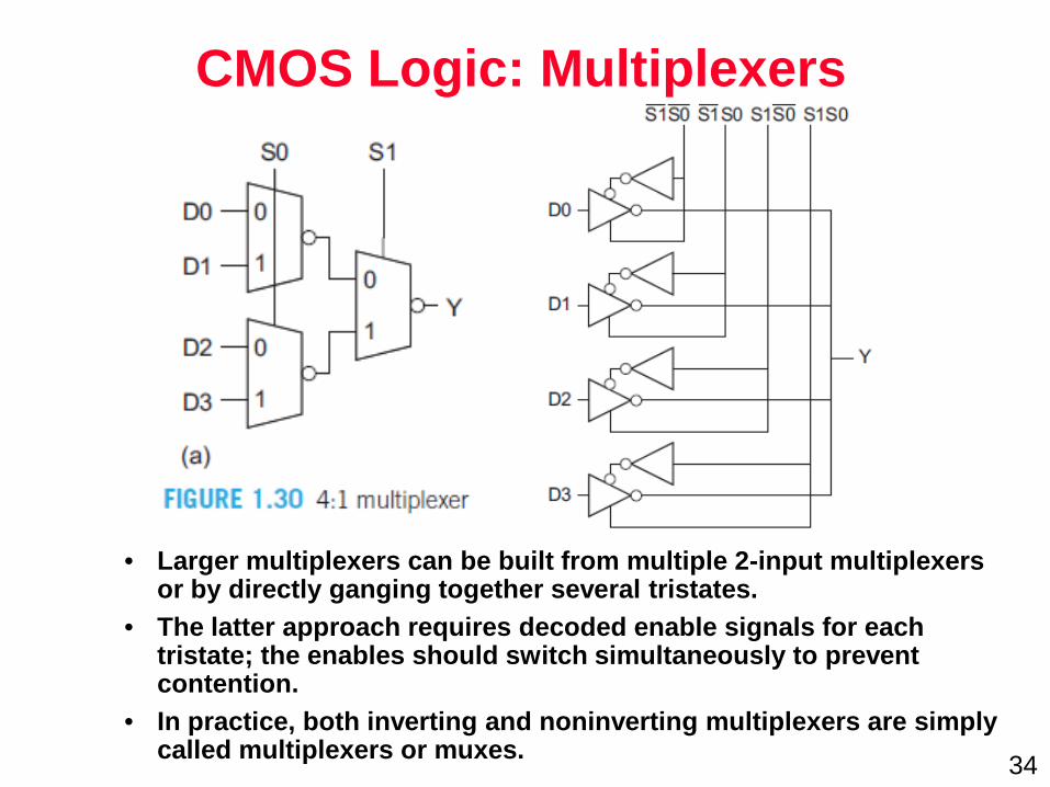
CMOS Logic: Multiplexers
• Multiplexers are key components in CMOS memory elements and data manipulation structures.
• A multiplexer chooses the output from among several inputs based on a select signal.
31

CMOS Logic: Multiplexers
• Nonrestoring multiplexer – Two transmission gates can be tied together to form a compact
2-input multiplexer.
32

CMOS Logic: Multiplexers
• Restoring, inverting multiplexer: – (a) compound gate – (b) gang together two tristate inverters
• The tristate approach is slightly more compact and faster because it requires less internal wire.
33
CMOS Logic: Multiplexers
• Larger multiplexers can be built from multiple 2-input multiplexers or by directly ganging together several tristates.
• The latter approach requires decoded enable signals for each tristate; the enables should switch simultaneously to prevent contention.
• In practice, both inverting and noninverting multiplexers are simply called multiplexers or muxes. 34
CMOS Logic: Sequential Circuits
• Combinational circuits – Outputs depend only on the current inputs.
• Sequential circuits – have memory – Outputs depend on both current and previous inputs – Latch and flip-flop
35

CMOS Logic: Sequential Circuits: D latch
• D latch: 2-input multiplexer and two inverters – when CLK = 1, it is transparent, Q follows D. – when CLK = 0, it becomes opaque, Q retains its previous value and
ignores changes in D. – Level sensitive latch: the state of the output is dependent on the level
of the clock signal » positive-level-sensitive latch, negative-level-sensitive
36

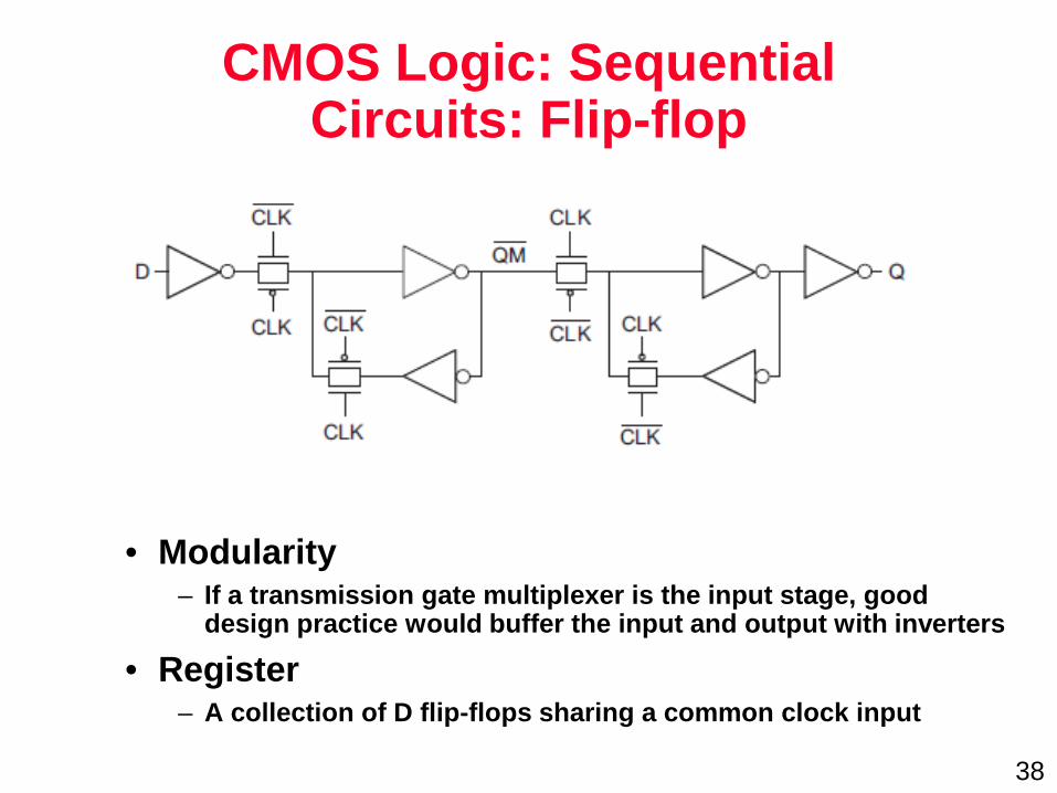
CMOS Logic: Sequential Circuits: Flip-flop
• Edge-triggered flip-flop – 1 negative-sensitive latch + 1 positive-sensitive latch – The first latch stage is called the master and the second is
called the slave. 37
CMOS Logic: Sequential Circuits: Flip-flop
• Modularity – If a transmission gate multiplexer is the input stage, good
design practice would buffer the input and output with inverters
• Register – A collection of D flip-flops sharing a common clock input
38

CMOS Logic: Sequential Circuits: Flip-flop
• Hold time problem – Clock skew: if one flip-flop triggers early and another triggers late
because of variations in clock arrival times – Hold-time problems can be avoided altogether by distributing a
two-phase nonoverlapping clock. 39