Embed Size (px)
Citation preview

Presented By
Anindya Sundar Dhar
IEP on Technology CAD (12-17th May 2008)
VLSI Architecture Design

Basic VLSI Design Flow
SYSTEM SPECIFICATION
ARCHITECTURAL DESIGN
LOGIC DESIGN
CIRCUIT DESIGN
DEVICE DESIGNLAYOUT
(Algorithmic Level)
(Register Transfer Level)
(Gate Level)
(Transistor Level)- - - - - - - - - - - - - - - - - -
Physical Design
FABRICATIONON-WAFER TESTING
PACKAGING
CHIP TESTING

Simulations at various levels
SYSTEM SPECIFICATION
ARCHITECTURAL DESIGN
LOGIC DESIGN
CIRCUIT DESIGN
DEVICE DESIGNLAYOUT
FABRICATIONON-WAFER TESTING
PACKAGING
CHIP TESTING
(Functional Simulation)
(Block level Simulation)
(Logic Simulation)
(Circuit Simulation)
(Device Simulation)
(Process Simulation)
(Fault Simulation)

OPTIMIZATION PROBLEM
Often they are considered to be constraint-satisfying problemrather than optimization problem.
SPEED
AREA
POWER
PRIMARY OBJECTIVE FUNCTIONS
The actual cost function involving these factorsdepends on specific application.
Design challenge is to have a better trade-off.

Concept of Hierarchy
• Continent• Country• State• District• City/Town/Village• House• Room• Wall• Brick• … …
• System• Subsystem• Functional unit• Functional subunit• Flip flop/MUX/Adder• Gate• Transistor• Device structure• … …

TOP DOWN
BOTTOM UP
DESIGN APPROACHES
ROOT NODE
LEAF CELLS

Constraint flow
Backannotation
FLOW OF CONSTRAINTS AND BACKANNOTATIONS
System Specification(Speed, Area, Power etc.)
Leaf cell parameters( Characterization data )

CORE
A TYPICAL CHIP SHOWING CORE AREA AND PADS
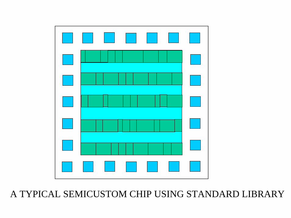
A TYPICAL SEMICUSTOM CHIP USING STANDARD LIBRARY

A TYPICAL CUSTOM CHIP

Standard cell fishbone structure
VDD
VSS
p-diff
n-diff
VSS
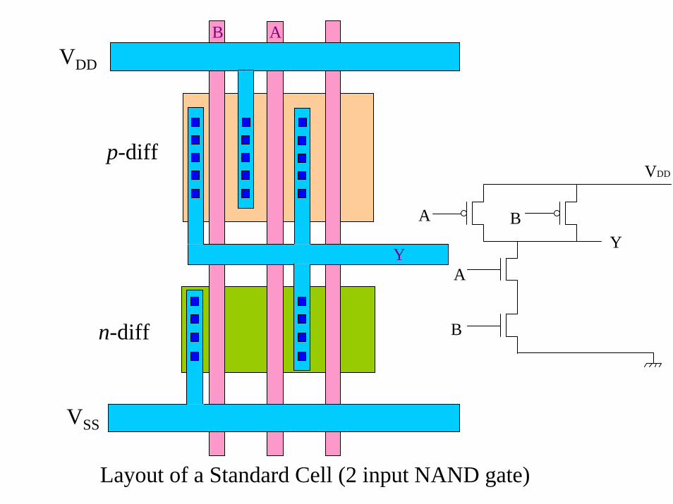
Layout of a Standard Cell (2 input NAND gate)
p-diff
n-diff
VDD
VSS
VDD
AY
A
B
B
B A
Y

OPTIMIZATION AT ALGORITHMIC LEVEL
EXAMPLE 1 : DISCRETE FOURIER TRANSFORM (DFT)O(N ) [ Unoptimized ]
FAST FOURIER TRANSFORM (FFT)O(N log N) [ Optimized ]
2
2
EXAMPLE 2 : Sum of Natural Numbers
S = 1 + 2 + 3 + . . . . . . . . + NS = N(N + 1) / 2
⇒ (N − 1) Additions⇒ 1 Increment and
1 Multiplication( Division by 2 is a mere SHIFT
in binary arithmetic )

OPTIMIZATION AT ARCHITECTURAL LEVEL
input NS = 0for i = 1 to N
S = S + inext ioutput S
N Si
input NS = 0for i = N downto 1
S = S + inext ioutput S
i S
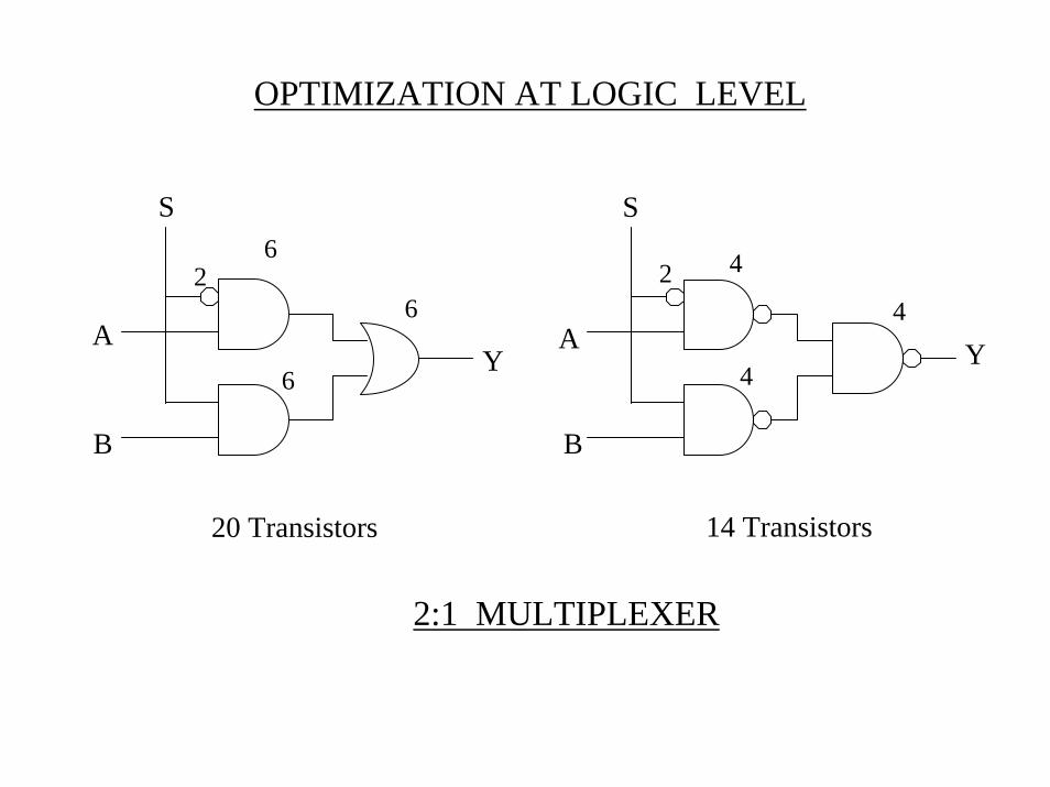
OPTIMIZATION AT LOGIC LEVEL
20 Transistors
2:1 MULTIPLEXER
4
4
42
S
B
A Y
14 Transistors
6
6
62
S
A
B
Y

OPTIMIZATION AT CIRCUIT LEVEL
2:1 MULTIPLEXER USING TRANSMISSION GATE LOGIC
S
S
S
A
B
Y
6 Transistors(including 2 for inverting S)
S

A
A
B
B
C
C
D
D
VDD
Y
Y = (AB + C)D
16 Transistors 8 Transistors
Optimized transistor level realization of Boolean function
ABCD
Y

OPTIMIZATION WITH RESPECT TO VARIOUS OBJECTIVE FUNCTIONS
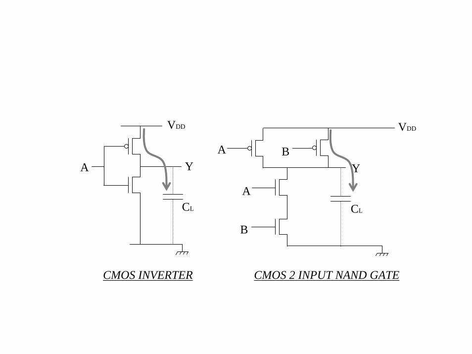
SPEED@LOGIC LEVEL
POWER@LOGIC LEVEL

VDD VDD
AA
Y
A
B
B
CL
Y
CL
CMOS INVERTER CMOS 2 INPUT NAND GATE
VDD
Y
CL
VDD
AA
Y
A
B
B
CL
CMOS INVERTER CMOS 2 INPUT NAND GATECMOS INVERTER CMOS 2 INPUT NAND GATE

VDD VDD
AA
Y
A
B
B
CL
Y
CL
CMOS INVERTER CMOS 2 INPUT NAND GATECMOS INVERTER CMOS 2 INPUT NAND GATE

APPLICATION SPECIFIC INTEGRATED CIRCUITS
DIGITAL
ANALOG
MIXED SIGNAL

ANALOG VLSI
Where it differs from theDesign with discrete componentsin a PCB or a breadboard?
• In the early days of Integrated Circuits:⇒ absence of Capacitors
• At present: ⇒ various constraints:Technology [CMOS]Area [e.g. in SoC]Noise [e.g. in mixed signal design]

ANALOG VLSI
At present: various constraints:Technology [CMOS]Area [e.g. in SoC]Noise [e.g. in mixed signal design]
☺ overall improvements:Higher Packing density Low Power consumptionHigher BandwidthHigh degree of Matching

ANALOG VLSI
Where do we stand today ?Thermionic Valve
Discrete Transistor
Integrated Circuits
MSI VLSI & beyondLSI
• Millions of Transistors• Deep Submicron Technology• Quantum Devices (?)

ANALOG VLSI
Challenges for Everyone:
• System designer• Circuit designer• Device designer• Layout engineer• Fabrication team• Packaging people
♥ To push the performance limits

Resistors
Diffusion resistors
Polysilicon resistors
n-well resistors
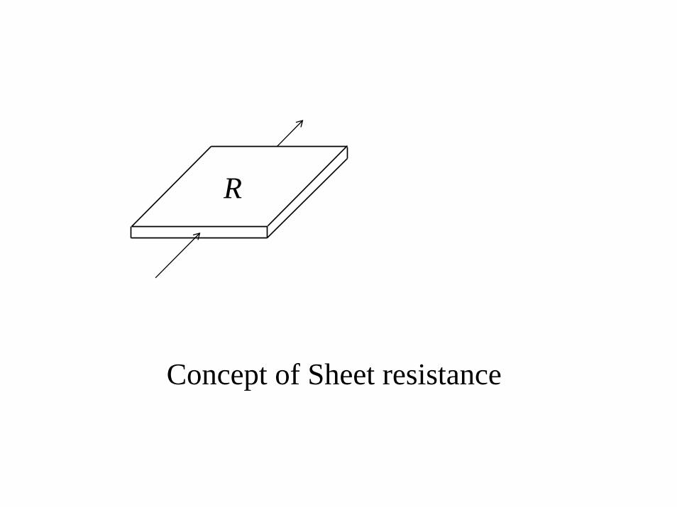
Concept of Sheet resistance
R

R R
R R
Sheet resistance (cont’d)

R
R
R
R
Sheet resistance (cont’d)

Capacitors
Poly-to-diffusion capacitor
Poly-to-poly capacitor
Metal-to-poly capacitor
Metal-to-metal capacitor

a 2a
2aa
1:4C1:C2 =
Issue of capacitor matching

a 2a
2aa
0.81:3.61 = 1:4.45C1:C2 =
0.9a
1.9a
1.9a
0.9a
Issue of capacitor matching (cont’d)

Issue of capacitor matching (cont’d)

Issue of capacitor matching (cont’d)
0.9a
0.9a
0.81:4×0.81 = 1:4C1:C2 =

Concept of Process corners
nMOS
Typ (VT = 500 mV)
Fast (VT = 400 mV)
Slow (VT = 600 mV)
pMOS
Typ (⏐VT ⏐= 550 mV)
Fast (⏐VT ⏐= 440 mV)
Slow (⏐VT ⏐ = 660 mV)
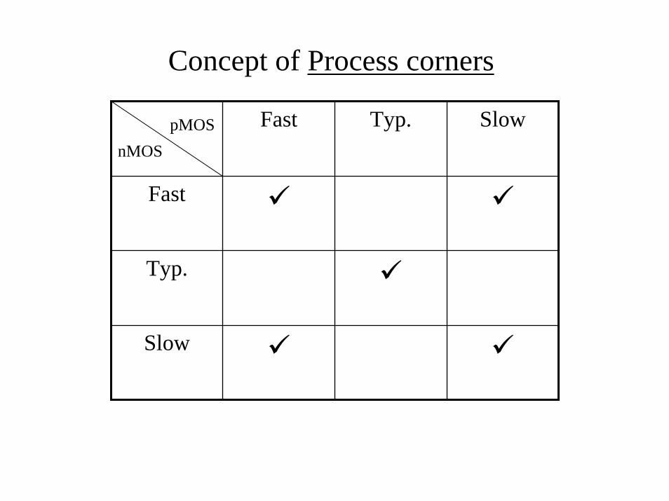
Concept of Process corners
pMOSnMOS
Fast Typ. Slow
Fast
Typ.
Slow

vin
io
RL
gm = io/ vin
+V
vout
Voltage gain: Av= vout/ vin = gm RL
STRUCTURE OF THE BASIC AMPLIFIER

rDC = v/i rAC = ∂v/∂i

CMOS Amplifierwith Active Load
CMOS Amplifier withCurrent Source Load
Push Pull CMOS Amplifier

Improper Layout Proper Layouts
Mobility could be differentin different directions

Variations along x and y directions

M1b
M1a M2b
M2a
Layout of Transistors for Differential Amplifier

M1b
M1a M2b
M2a
Power Device
Thermal contours

vin
io
+VDD
vout
Voltage gain: Av= vout/ vin= gmN/(gdsN+ gdsP)
Vbias
P-MOS
N-MOS
CMOS Amplifier with Current Source (Active) Load

vin
io
+VDD
vout
Voltage gain: Av= vout/ vin= (gmN+ gmP)/(gdsN+ gdsP)
N-MOS
P-MOS
CMOS Push Pull Amplifier

vin
io
+VDD
vout
N-MOS
P-MOS
It is interesting to note that the same circuit can work asan analog amplifier as well as a digital inverter
vin
vout

vin
+VDD
vout
N-MOS
P-MOS
Propagation delay of the digital inverter fully dependsupon the device parameters
CL
tpLH = Rp (Cout + CL )
tpHL = Rn (Cout + CL )

voutvin gmvin roRL
vout = ( ro⏐⏐RL ) gmvin
Low frequency model of an active device
io
vin
io
Three TerminalActive Device ≡

voutvin gmvin roRL
vout = ( ro⏐⏐RL ) gmvin
Typical High frequency model of an active device
Cin
CMiller io
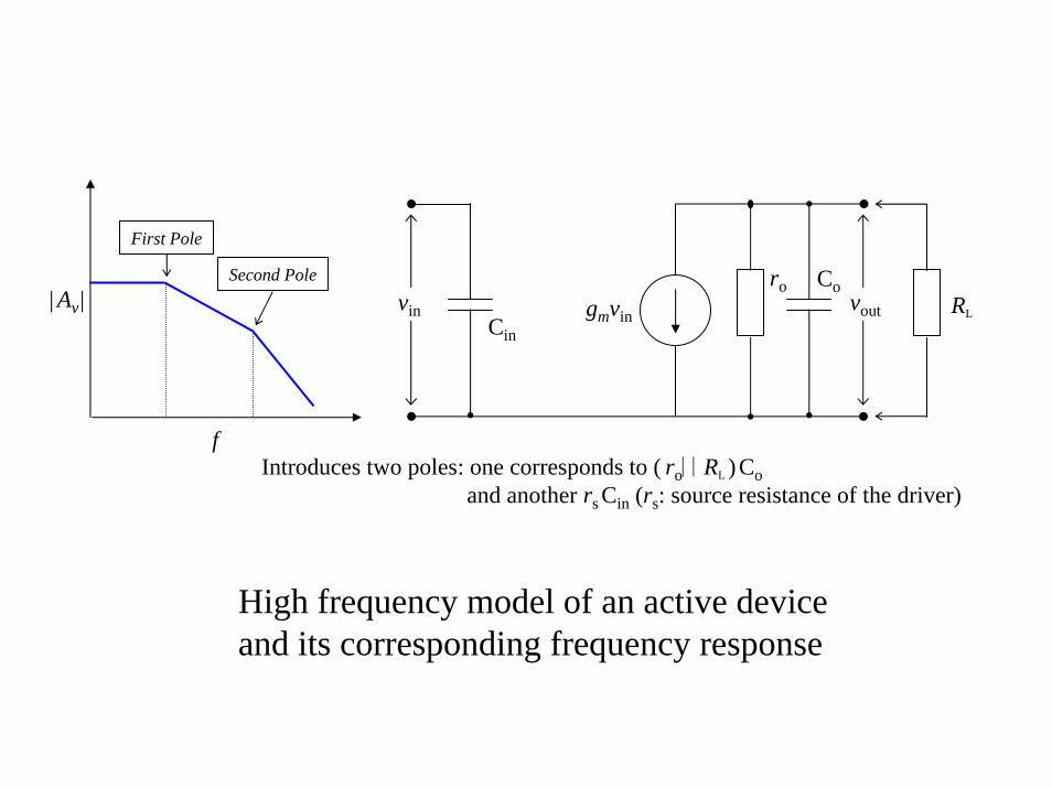
voutvin gmvin
roRL
High frequency model of an active deviceand its corresponding frequency response
Cin
Co
Introduces two poles: one corresponds to ( ro⏐⏐RL )Coand another rs Cin (rs: source resistance of the driver)
f
|Av|
First Pole
Second Pole

Conclusions
• Quantum Devices are likely to take overthe arena of VLSI Design in near future
• Device Modeling and Process Modelingare extremely important in predictingthe VLSI System Performance