Embed Size (px)
Citation preview

Video Processing Subsystem v1.0
Product Guide
Vivado Design Suite
PG231 November 18, 2015
Video Processing Subsystem v1.0 www.xilinx.com 2PG231 November 18, 2015
Table of ContentsIP Facts
Chapter 1: OverviewIntroduction . . . . . . . . . . . . . . . . . . . . . . . . . . . . . . . . . . . . . . . . . . . . . . . . . . . . . . . . . . . . . . . . . . . . . . 5Feature Summary. . . . . . . . . . . . . . . . . . . . . . . . . . . . . . . . . . . . . . . . . . . . . . . . . . . . . . . . . . . . . . . . . . 5Applications . . . . . . . . . . . . . . . . . . . . . . . . . . . . . . . . . . . . . . . . . . . . . . . . . . . . . . . . . . . . . . . . . . . . . . 6Licensing and Ordering Information . . . . . . . . . . . . . . . . . . . . . . . . . . . . . . . . . . . . . . . . . . . . . . . . . . . 6
Chapter 2: Product SpecificationStandards . . . . . . . . . . . . . . . . . . . . . . . . . . . . . . . . . . . . . . . . . . . . . . . . . . . . . . . . . . . . . . . . . . . . . . . . 8Performance. . . . . . . . . . . . . . . . . . . . . . . . . . . . . . . . . . . . . . . . . . . . . . . . . . . . . . . . . . . . . . . . . . . . . . 8Resource Utilization. . . . . . . . . . . . . . . . . . . . . . . . . . . . . . . . . . . . . . . . . . . . . . . . . . . . . . . . . . . . . . . . 8Port Descriptions . . . . . . . . . . . . . . . . . . . . . . . . . . . . . . . . . . . . . . . . . . . . . . . . . . . . . . . . . . . . . . . . . . 9
Chapter 3: Designing with the CoreGeneral Design Guidelines . . . . . . . . . . . . . . . . . . . . . . . . . . . . . . . . . . . . . . . . . . . . . . . . . . . . . . . . . 14Clocking. . . . . . . . . . . . . . . . . . . . . . . . . . . . . . . . . . . . . . . . . . . . . . . . . . . . . . . . . . . . . . . . . . . . . . . . . 31Resets . . . . . . . . . . . . . . . . . . . . . . . . . . . . . . . . . . . . . . . . . . . . . . . . . . . . . . . . . . . . . . . . . . . . . . . . . . 32
Chapter 4: Design Flow StepsCustomizing and Generating the Core . . . . . . . . . . . . . . . . . . . . . . . . . . . . . . . . . . . . . . . . . . . . . . . . 33Constraining the Core . . . . . . . . . . . . . . . . . . . . . . . . . . . . . . . . . . . . . . . . . . . . . . . . . . . . . . . . . . . . . 39Simulation . . . . . . . . . . . . . . . . . . . . . . . . . . . . . . . . . . . . . . . . . . . . . . . . . . . . . . . . . . . . . . . . . . . . . . 40Synthesis and Implementation . . . . . . . . . . . . . . . . . . . . . . . . . . . . . . . . . . . . . . . . . . . . . . . . . . . . . . 40
Chapter 5: Detailed Example DesignFull-fledged Video Processing Design . . . . . . . . . . . . . . . . . . . . . . . . . . . . . . . . . . . . . . . . . . . . . . . . . 41Scaler-only Video Processing Design . . . . . . . . . . . . . . . . . . . . . . . . . . . . . . . . . . . . . . . . . . . . . . . . . 42
Appendix A: Migrating and UpgradingUpgrading in the Vivado Design Suite . . . . . . . . . . . . . . . . . . . . . . . . . . . . . . . . . . . . . . . . . . . . . . . . 46
Appendix B: DebuggingFinding Help on Xilinx.com . . . . . . . . . . . . . . . . . . . . . . . . . . . . . . . . . . . . . . . . . . . . . . . . . . . . . . . . . 47
Send Feedback

Video Processing Subsystem v1.0 www.xilinx.com 3PG231 November 18, 2015
Debug Tools . . . . . . . . . . . . . . . . . . . . . . . . . . . . . . . . . . . . . . . . . . . . . . . . . . . . . . . . . . . . . . . . . . . . . 48Simulation Debug. . . . . . . . . . . . . . . . . . . . . . . . . . . . . . . . . . . . . . . . . . . . . . . . . . . . . . . . . . . . . . . . . 49Hardware Debug . . . . . . . . . . . . . . . . . . . . . . . . . . . . . . . . . . . . . . . . . . . . . . . . . . . . . . . . . . . . . . . . . 49Interface Debug . . . . . . . . . . . . . . . . . . . . . . . . . . . . . . . . . . . . . . . . . . . . . . . . . . . . . . . . . . . . . . . . . . 50
Appendix C: Application Software DevelopmentDriver . . . . . . . . . . . . . . . . . . . . . . . . . . . . . . . . . . . . . . . . . . . . . . . . . . . . . . . . . . . . . . . . . . . . . . . . . . 51Dependencies. . . . . . . . . . . . . . . . . . . . . . . . . . . . . . . . . . . . . . . . . . . . . . . . . . . . . . . . . . . . . . . . . . . . 51Architecture . . . . . . . . . . . . . . . . . . . . . . . . . . . . . . . . . . . . . . . . . . . . . . . . . . . . . . . . . . . . . . . . . . . . . 51Usage . . . . . . . . . . . . . . . . . . . . . . . . . . . . . . . . . . . . . . . . . . . . . . . . . . . . . . . . . . . . . . . . . . . . . . . . . . 53
Appendix D: Additional Resources and Legal NoticesXilinx Resources . . . . . . . . . . . . . . . . . . . . . . . . . . . . . . . . . . . . . . . . . . . . . . . . . . . . . . . . . . . . . . . . . . 55References . . . . . . . . . . . . . . . . . . . . . . . . . . . . . . . . . . . . . . . . . . . . . . . . . . . . . . . . . . . . . . . . . . . . . . 55Revision History . . . . . . . . . . . . . . . . . . . . . . . . . . . . . . . . . . . . . . . . . . . . . . . . . . . . . . . . . . . . . . . . . . 56Please Read: Important Legal Notices . . . . . . . . . . . . . . . . . . . . . . . . . . . . . . . . . . . . . . . . . . . . . . . . 56
Send Feedback

Video Processing Subsystem v1.0 www.xilinx.com 4PG231 November 18, 2015 Product Specification
IntroductionThe Video Processing Subsystem is a collection of video processing IP subcores, bundled together in hardware and software, abstracting the video processing pipe. It provides the end-user with an out of the box ready to use video processing core, without having to learn about the underlying complexities. The Video Processing Subsystem enables streamlined integration of various processing blocks including (but not limited to) scaling, deinterlacing, color space conversion and correction, chroma resampling, and frame rate conversion.
Features• One, two or four pixel-wide AXI4-Stream
video interface
• Video resolution support up to UHD at the 60 fps
• Run-time color space support for RGB, YUV 4:4:4, YUV 4:2:2, YUV 4:2:0
• 8, 10, 12, and 16 bits per component support
• Deinterlacing
• Scaling
• Color space conversion and correction
• Chroma resampling between YUV4:4:4, YUV 4:2:2, YUV 4:2:0
• Frame rate conversion using dropped/repeated frames
IP Facts
LogiCORE™ IP Facts Table
Core SpecificsSupported Device Family(1)
UltraScale+™ Families,UltraScale™ Architecture, Zynq®-7000, 7 Series
Supported User Interfaces AXI4-Lite, AXI4-Stream, AXI-MM
Resources See Table 2-1 through Table 2-2
Provided with CoreDesign Files Encrypted HLS C
Example Design Verilog
Test Bench Not Provided
Constraints File XDC
Simulation Model Source HDL
Supported S/W Driver(2) Standalone
Tested Design Flows(3)
Design Entry Vivado® Design Suite
Simulation For supported simulators, see theXilinx Design Tools: Release Notes Guide.
Synthesis Not Provided.
SupportProvided by Xilinx at the Xilinx Support web page
Notes: 1. For a complete list of supported devices, see the Vivado IP
catalog.2. Standalone driver details can be found in the SDK directory
(<install_directory>/doc/usenglish/xilinx_drivers.htm). Linux OS and driver support information is available from the Xilinx Wiki page.
3. For the supported versions of the tools, see theXilinx Design Tools: Release Notes Guide.
Send Feedback

Video Processing Subsystem v1.0 www.xilinx.com 5PG231 November 18, 2015
Chapter 1
Overview
IntroductionThe Video Processing Subsystem enables streamlined integration of various processing blocks including (but not limited to) scaling, deinterlacing, color space conversion and correction, chroma resampling, and frame rate conversion.
Feature SummaryThe Video Processing Subsystem has the following features:
• One, two, or four pixel-wide video interface
• Run-time color space support for RGB, YUV 4:4:4, YUV 4:2:2, YUV 4:2:0
• 8, 10, 12, and 16 bits per component support
• Deinterlacing
• Scaling
• Color space conversion and correction
• Chroma resampling between YUV4:4:4, YUV 4:2:2, YUV 4:2:0
• Frame rate conversion
• Two possible configurations: Scaler only or full fledged functionality
• Supports resolutions up to 4096 x 2160
The Video Processing Subsystem is a hierarchical IP that bundles a collection of video processing IP subcores and outputs them as a single IP. The video processing IP subsystem has design time configurability in terms of performance and quality. You can configure the subsystem IP through one single graphical user interface. A preview of this GUI is shown in Figure 4-1.
All video processing IP subcores have been developed using Vivado HLS.
Send Feedback

Video Processing Subsystem v1.0 www.xilinx.com 6PG231 November 18, 2015
Chapter 1: Overview
Applications• Color space (RGB/YUV) and format (YUV 4:4:4/4:2:2/4:2:0) conversion.
• Scale up and down up to 4k2k at 60 Hz.
• Zoom mode, where in a user defined window, the input stream is scaled to panel resolution.
• Picture-In-Picture mode where in the input stream is scaled down to a user defined window size and displayed at the user defined co-ordinates on the panel.
• Ability to paint the PIP background to a defined color.
• Interlaced to progressive conversion.
• Frame rate conversion.
° Drop frames if input rate > output rate.
° Repeat frames if output rate < input rate.
Licensing and Ordering Information
License CheckersIf the IP requires a license key, the key must be verif ied. The Vivado® design tools have several license checkpoints for gating licensed IP through the flow. If the license check succeeds, the IP can continue generation. Otherwise, generation halts with error. License checkpoints are enforced by the following tools:
• Vivado synthesis
• Vivado implementation
• write_bitstream (Tcl command)
IMPORTANT: IP license level is ignored at checkpoints. The test confirms a valid license exists. It does not check IP license level.
Send Feedback

Video Processing Subsystem v1.0 www.xilinx.com 7PG231 November 18, 2015
Chapter 1: Overview
License TypeThis Xilinx LogiCORE™ IP module is provided under the terms of the Xilinx Core License Agreement. The module is shipped as part of the Vivado® Design Suite. For full access to all core functionalities in simulation and in hardware, you must purchase a license for the core. There is no evaluation version of the core. Contact your local Xilinx sales representative for information about pricing and availability.
For more information, visit the Video Processing Subsystem product web page.
www.xilinx.com/products/intellectual-property/video-processing-subsystem.html
Information about other Xilinx LogiCORE IP modules is available at the Xilinx Intellectual Property page. For information on pricing and availability of other Xilinx LogiCORE IP modules and tools, contact your local Xilinx sales representative.
Send Feedback

Video Processing Subsystem v1.0 www.xilinx.com 8PG231 November 18, 2015
Chapter 2
Product Specification
StandardsThe Video Processing Subsystem core is compliant with the AXI4-Stream Video Protocol and AXI4-Lite interconnect standards. Refer to the Video IP: AXI Feature Adoption section of the Vivado AXI Reference Guide (UG1037) [Ref 8] for additional information.
Performance
LatencyThe latency of the Scaler-only configuration depends on the number of taps used in the vertical scaler. For example, a 6-tap vertical scaler introduces 4 video lines of delay. In full-fledged configuration, the latency depends on the format of the video. In progressive video, the latency is 1 full frame time plus several lines because the video DMA engine is used in the data flow and programmed to read one frame buffer behind the write frame buffer location. In interlaced video, 1 field additional delay is being incurred by the deinterlacer algorithm.
Resource UtilizationTable 2-1 and Table 2-2 show representative resource utilization for the two supported configurations.
Table 2-1: Resource Utilization for Scaler-only Configuration
FF LUTs BRAMs DSPs
6,101 7,512 45 72
Table 2-2: Resource Utilization for Full-fledged Configuration
FF LUTs BRAMs DSPs
33,538 35,440 138 125
Send Feedback

Video Processing Subsystem v1.0 www.xilinx.com 9PG231 November 18, 2015
Chapter 2: Product Specification
Port DescriptionsFigure 2-1 shows the Video Processing Subsystem IP diagram in its full-fledged configuration. The IP has four AXI interfaces:
• AXI4-Stream streaming video input (s_axis)
• AXI4-Stream streaming video output (m_axis)
• AXI-MM memory interface (m_axi_mm)
• AXI-Lite control interface (s_axi_ctrl).
The AXI Streaming, AXI Memory, and AXI Lite interfaces can be run at their own clock rate, therefore, three separate clock interfaces are provided named aclk_axis, aclk_axi_mm, and aclk_ctrl, respectively. The aresetn_ctrl signal is the reset signal of the IP, and aresetn_io_axis is an outgoing signal that can be used to hold IPs in reset when the Video Processing Subsystem IP is not ready to consume data on streaming input. Finally, deint_field_id signal indicates field polarity in case of interlaced operation.
AXI4-Stream VideoThe video processing IP subsystem has AXI4-Stream video input and output interfaces named s_axis and m_axis, respectively. These interfaces follow the interface specification as defined in the Video IP chapter of the Vivado AXI Reference Guide (UG1037) [Ref 8]. The video AXI4-Stream interface can be single, dual, or quad pixels per clock and
X-Ref Target - Figure 2-1
Figure 2-1: Full-fledged Video Processing Subsystem IP
Send Feedback
Video Processing Subsystem v1.0 www.xilinx.com 10PG231 November 18, 2015
Chapter 2: Product Specification
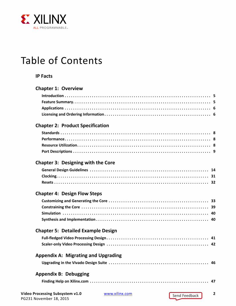
can support 8, 10, 12, or 16 bits per component. For example, the pixel mapping per color format and bus signals for 10 bits per component are shown in Table 2-3 through Table 2-7.
1. IP always generates three video components even if the video format is set to be YUV 4:2:2 at run-time. The unused components can be set to zero.
Table 2-8 shows the interface signals for input and output AXI4-Stream video streaming interfaces.
Table 2-3: Dual Pixels per Clock, 10 Bits per Component Mapping for RGB
63:60 59:50 49:40 39:30 29:20 19:10 9:0
zero padding R1 B1 G1 R0 B0 G0
Table 2-4: Dual Pixels per Clock, 10 Bits per Component Mapping for YUV 4:4:4.
63:60 59:50 49:40 39:30 29:20 19:10 9:0
zero padding V1 U1 Y1 V0 U0 Y0
Table 2-5: Dual Pixels per Clock, 10 Bits per Component Mapping for YUV 4:2:2(1)
63:60 59:50 49:40 39:30 29:20 19:10 9:0
zero padding zero padding zero padding V0 Y1 U0 Y0
Table 2-6: Dual Pixels per Clock, 10 Bits per Component Mapping for YUV 4:2:0, for Even Lines
63:60 59:50 49:40 39:30 29:20 19:10 9:0
zero padding Y3 U2 Y2 Y1 U0 Y0
Table 2-7: Dual Pixels per Clock, 10 Bits per Component Mapping for YUV 4:2:0, for Odd Lines
63:60 59:50 49:40 39:30 29:20 19:10 9:0
zero padding zero padding zero padding Y2 Y1 V0 Y0
Table 2-8: AXI4 Streaming Interface Signals
Name Direction Width Description
s_axis_tdata In floor(((3 x bits_per_component x pixels_per_clock) + 7) / 8) x 8
Input Data
s_axis_tready Out 1 Input Ready
s_axis_tvalid In 1 Input Valid
s_axis_tdest In 1 Input data routing identif ier
s_axis_tkeep In (s_axis_video_tdata width)/8 Input byte qualif ier that indicates whether the content of the associated byte of TDATA is processed as part of the data stream
s_axis_tlast In 1 Input End of Line
Send Feedback

Video Processing Subsystem v1.0 www.xilinx.com 11PG231 November 18, 2015
Chapter 2: Product Specification
Both video streaming interfaces run at the video stream clock speed aclk_axis.
AXI-MM Memory InterfaceThe video DMA read and write ports and the deinterlacer read and write ports are concentrated by an AXI-MM cross-bar interconnect such that there is only one AXI-MM interface on the boundary of the subsystem. The AXI-MM interface runs on the aclk_axi_mm clock domain. The signals follow the specif ication as defined in the AXI Reference Guide [Ref 8]. The AXI-MM Memory interface is only present with the full-fledged functionality configuration. The Scaler-only configuration does not require access to external memory.
AXI-Lite Control InterfaceTable 2-9 shows the AXI-Lite control interface signals. This interface runs at the aclk_ctrl clock. Control of the video processing pipe is only supported through the video processing IP subsystem driver.
s_axis_tstrb In (s_axis_video_tdata width)/8 Input byte qualif ier that indicates whether the content of the associated byte of TDATA is processed as a data byte or a position byte
s_axis_tuser In 1 Input Start of frame
m_axis_tdata Out floor(((3 x bits_per_component x pixels_per_clock) + 7) / 8) x 8
Output Data
m_axis_tdest Out 1 Output data routing identif ier
m_axis_tid Out 1 Output data stream identif ier
m_axis_tkeep Out (m_axis_video_tdata width)/8 Output byte qualif ier that indicates whether the content of the associated byte of TDATA is processed as part of the data stream
m_axis_tlast Out 1 Output End of Line
m_axis_tready In 1 Output Ready
m_axis_tstrb Out (m_axis_video_tdata width)/8 Output byte qualif ier that indicates whether the content of the associated byte of TDATA is processed as a data byte or a position byte
m_axis_tuser Out 1 Output Start of frame
m_axis_tvalid Out 1 Output Valid
Table 2-8: AXI4 Streaming Interface Signals (Cont’d)
Name Direction Width Description
Send Feedback

Video Processing Subsystem v1.0 www.xilinx.com 12PG231 November 18, 2015
Chapter 2: Product Specification
Clocks and ResetsTable 2-10 provides an overview of the clocks and resets. See section Clocking in Chapter 3 for more information.
Table 2-9: AXI Lite Control Interface
Name Direction Width Description
s_axi_ctrl_aresetn In 1 Reset
s_axi_ctrl_aclk In 1 Clock
s_axi_ctrl_awaddr In 18 Write address
s_axi_ctrl_awprot In 3 Write address protection
s_axi_ctrl_awvalid In 1 Write address valid
s_axi_ctrl_awready Out 1 Write address ready
s_axi_ctrl_wdata In 32 Write data
s_axi_ctrl_wstrb In 4 Write data strobe
s_axi_ctrl_wvalid In 1 Write data valid
s_axi_ctrl_wready Out 1 Write data ready
s_axi_ctrl_bresp Out 2 Write response
s_axi_ctrl_bvalid Out 1 Write response valid
s_axi_ctrl_bready In 1 Write response ready
s_axi_ctrl_araddr In 18 Read address
s_axi_ctrl_arprot In 3 Read address protection
s_axi_ctrl_arvalid In 1 Read address valid
s_axi_ctrl_aready Out 1 Read address ready
s_axi_ctrl_rdata Out 32 Read data
s_axi_ctrl_rresp Out 2 Read data response
s_axi_ctrl_rvalid Out 1 Read data valid
s_axi_ctrl_rready In 1 Read data ready
Table 2-10: Clocks and Resets
Name Direction Width Description
Clocks
aclk_axis In 1 Clock at which AXI4-Stream input and output are running.
aclk_ctrl In 1 AXI-Lite clock for CPU control interface.
aclk_axi_mm In 1 Clock at which AXI-MM interface is running.
Send Feedback

Video Processing Subsystem v1.0 www.xilinx.com 13PG231 November 18, 2015
Chapter 2: Product Specification
Field PolarityThe deint_field_id signal indicates the polarity of the incoming f ield when the input video is interlaced. This signal is only used by the deinterlacer with interlaced data. This signal is ignored for progressive video inputs.
Resets
aresetn_ctrl In 1 Reset, associated with aclk_ctrl (active Low). The aresetn_ctrl signal resets the entire IP including the data path and AXI4-Lite registers.
aresetn_io_axis Out 1 Used to hold upstream logic in reset while the Video Processing Subsystem is not to consume data on streaming input (active Low).
Table 2-11: Field Polarity
Name Direction Width Description
deint_field_id In 1 Field polarity, odd is low, high is even
Table 2-10: Clocks and Resets (Cont’d)
Name Direction Width Description
Send Feedback

Video Processing Subsystem v1.0 www.xilinx.com 14PG231 November 18, 2015
Chapter 3
Designing with the CoreThis chapter includes guidelines and additional information to facilitate designing with the core.
General Design GuidelinesThe Video Processing Subsystem is a collection of individual subcore IPs packaged as a hierarchical IP and configured through one single graphical user interface (GUI). The Subsystem can perform the following functions: deinterlacing, scaling, frame rate conversion, color space conversion and correction, and chroma resampling.
Appendix C, Application Software Development describes how to integrate the associated Video Processing Subsystem API into a software application.
DeinterlacingThe Video Deinterlacer converts live incoming interlaced video streams into progressive video streams. Interlaced images have temporal motion between the two f ields that comprise an interlaced frame. The conversion to a progressive format recombines these two f ields into one single progressive scan frame. The weaving of interlaced video streams results in unsightly motion artifacts in the progressive output image. For this reason, the Video Deinterlacer uses three f ield buffers, and produces progressive frames based on a combination of spatial and temporal processing.
Features
The Video Deinterlacer is a low-cost basic Deinterlacer that uses three f ield buffers. The following list is a summary of the supported features:
• Always uses memory interface.
• Support for RGB, YUV 4:4:4, and YUV 4:2:2.
• 8, 10, 12, or 16 bits per component.
Send Feedback

Video Processing Subsystem v1.0 www.xilinx.com 15PG231 November 18, 2015
Chapter 3: Designing with the Core
ScalingVideo scaling is the process of converting an input color image of dimensions Xin pixels by Yin lines to an output color image of dimensions Xout pixels by Yout lines. The IP converts a specif ied rectangular area of an input digital video image from the original sampling grid to a desired target sampling grid.
The input image must be provided in raster scan format (left to right and top to bottom). The valid outputs are also given in this order.
Video scaling is a form of 2-D filter operation which can be approximated with the equation shown in Equation 3-1.
Equation 3-1
In this equation, x and y are discrete locations on a common sampling grid; Pixout (x, y) is an output pixel that is being generated at location (x, y); Pixin (x, y) is an input pixel being used as part of the input scaler aperture; Coef (i, j) is an array of coefficients that depend upon the application; and HTaps and VTaps are the number of horizontal and vertical taps in the f ilter, respectively.
The coefficients in this equation represent weights applied to the set of input samples chosen to contribute to one output pixel, according to the scaling ratio.
Features
The Scaler comes in three different quality levels each at different levels of resource usage.
• Bilinear scaling is the cheapest implementation of the Scaler that uses bilinear interpolation to calculate pixels. Bilinear interpolation produces a greater number of interpolation artifacts (such as aliasing, blurring, and edge halos) than more computationally demanding techniques such as bicubic interpolation.
• Bicubic scaling is a more demanding compared to bilinear scaling, and produces smoother pictures with less artifacts. Compared to bilinear interpolation, which only takes 2 x 2 pixels into account, bicubic interpolation considers a 4 x 4 pixel area.
• The polyphase concept is explained in Polyphase Scaling. The picture quality (and resource usage) of a polyphase scaler depends largely on the number of f ilter taps used and number of f ilter phases used. Polyphase scaling offers the highest quality but also has the highest resource utilization.
Send Feedback

Video Processing Subsystem v1.0 www.xilinx.com 16PG231 November 18, 2015
Chapter 3: Designing with the Core
The following list is a summary of the supported features:
• Polyphase, bicubic, or bilinear scaling modes
• 6, 8, 10, or 12-tap 64 phase polyphase scaling
• Support for RGB, YUV 4:4:4, and YUV 4:2:2.
• 8, 10, 12, or 16 bits per video component
Polyphase ScalingFor scaling, the input and output sampling grids are assumed to be different, in contrast to the example in the preceding section. To express a discrete output pixel in terms of input pixels, it is necessary to know or estimate the location of the output pixel relative to the closest input pixels when superimposing the output sampling grid upon the input sampling grid for the equivalent 2-D space. With this knowledge, the algorithm approximates the output pixel value by using a f ilter with coefficients weighted accordingly. Filter taps are consecutive data-points drawn from the input image.
As an example, Figure 3-1 shows a desired 5x5 output grid ("O") superimposed upon an original 6x6 input grid ("X"), occupying common space. In this case, estimating for output position (x, y) = (1, 1), shows the input and output pixels to be co-located. You can weigh the coeff icients to reflect no bias in either direction, and can even select a unity coefficient set. Output location (2, 2) is offset from the input grid in both vertical and horizontal dimensions. Coefficients can be chosen to reflect this, most likely showing some bias towards input pixel (2, 2), etc. Filter characteristics can be built into the f ilter coeff icients by appropriately applying anti-aliasing low-pass f ilters.
The space between two consecutive input pixels in each dimension is conceptually partitioned into a number of bins or phases. The location of any arbitrary output pixel always falls into one of these bins, thus defining the phase of coefficients used. The f ilter
X-Ref Target - Figure 3-1
Figure 3-1: 5x5 Output Grid (“O”) Super-imposed over 6x6 Input Grid (“X”)
Send Feedback

Video Processing Subsystem v1.0 www.xilinx.com 17PG231 November 18, 2015
Chapter 3: Designing with the Core
architecture should be able to accept any of the different phases of coeff icients, changing phase on a sample-by-sample basis.
A single dimension is shown in Figure 3-2. As illustrated in this f igure, the five output pixels shown from left to right could have the phases 0, 1, 2, 3, 0.
The examples in Figure 3-1 and Figure 3-2 show a conversion where the ratio Xin/Xout = Yin/Yout = 5/4. This ratio is known as the Scaling Factor, or SF. The horizontal and vertical Scaling Factors can be different. A typical example is drawn from the broadcast industry, where some footage can be shot using 720p (1280 x 720), but the cable operator needs to deliver it as per the broadcast standard 1080p (1920 x 1080). The SF becomes 2/3 in both H and V dimensions.
Typically, when Xin > Xout, this conversion is known as horizontal down-scaling (SF > 1). When Xin < Xout, it is known as horizontal up-scaling (SF < 1).
The set of coeff icients constitute filter banks in a polyphase filter whose frequency response is determined by the amount of scaling applied to the input samples. The phases of the filter represent subfilters for the set of samples in the f inal scaled result.
The number of coeff icients and their values are dependent upon the required low-pass, anti-alias response of the scaling f ilter; for example, smaller scaling ratios require lower passbands and more coefficients. Filter design programs based on the Lanczos algorithm are suitable for coefficient generation. Moreover, MATLAB® product fdatool/fvtool can be used to provide a wider f ilter design toolset.
A direct implementation of Equation 1 suggests that a filter with VTaps x HTaps multiply operations per output are required. However, the Xilinx® Video Scaler supports only separable f ilters, which completes an approximation of the 2-D operation using two 1-D stages in sequence - a vertical f ilter (V-filter) stage and a horizontal f ilter (H-filter) stage. The intermediate results of the f irst stage are fed sequentially to the second stage.
The vertical f ilter stage filters only in the vertical domain, for each incrementing horizontal raster scan position x, creating an intermediate result described as VPix (Equation 3-2).
Equation 3-2
X-Ref Target - Figure 3-2
Figure 3-2: Super-imposed Grids for 1 Dimension
VPixint x y,[ ] Pixin x y, VTaps 2⁄( )– i+[ ] Vcoef i[ ]×VTaps 1–
i 0=
=
Send Feedback
Video Processing Subsystem v1.0 www.xilinx.com 18PG231 November 18, 2015
Chapter 3: Designing with the Core
The output result of the vertical component of the scaler f ilter is input into the horizontal f ilter with the appropriate rounding applied. The separation means this can be reduced to the shown VTaps and HTaps multiply operations, saving FPGA resources (Equation 3-3).
Equation 3-3
Notice that the differences between the Bilinear, Bicubic, and Polyphase architectures are not only marked by a difference in coeff icients only but with the implementation of optimized architectures for Bilinear and Bicubic scaling.
Video DMA EngineMany video applications require frame buffers to handle frame rate changes or changes to the image dimensions (scaling or cropping). The Video DMA engine, which uses the Xilinx AXI Video Direct Memory Access IP, is designed to allow for eff icient high-bandwidth access between AXI4-Stream video interface and AXI4-MM interface.
Features
The Video DMA engine within the full-fledged configuration of the Video Processing Subsystem IP is used to enable frame rate conversion and also more advanced scaling use cases like crop and zoom and scale to picture in picture.
Frame Rate Conversion
Frame rate conversion is implemented by dropping or repeating frames. The DMA engine keeps track of 4 frame buffers that are being written to in a cyclic fashion. The read portion of the video data flow remains exactly 1 frame behind the write pointer. In case the incoming frame rate is higher than the outgoing frame rate, the write pointer advances more frequently than the read pointer, meaning that frames are skipped. Similarly, the read pointer is always one frame behind the write pointer even in case the outgoing frame rate is higher than the incoming frame rate. In this case, frames are repeated.
Crop and Zoom
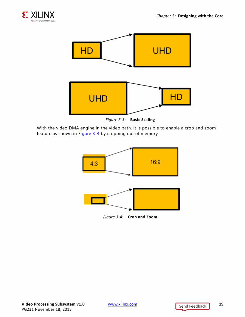
Another use of the video DMA engine is to enable advanced scaling use cases like crop and zoom, and scale to picture in picture. Without the use of memory, only basic scaling can be performed from one resolution to another resolution, as shown in Figure 3-3.
Pixout x y,[ ] VPixint x HTaps 2⁄( )– i+ y,[ ] Hcoef i[ ]×HTaps 1–
i 0=
=
Send Feedback
Video Processing Subsystem v1.0 www.xilinx.com 19PG231 November 18, 2015
Chapter 3: Designing with the Core
With the video DMA engine in the video path, it is possible to enable a crop and zoom feature as shown in Figure 3-4 by cropping out of memory.
X-Ref Target - Figure 3-3
Figure 3-3: Basic Scaling
X-Ref Target - Figure 3-4
Figure 3-4: Crop and Zoom
Send Feedback

Video Processing Subsystem v1.0 www.xilinx.com 20PG231 November 18, 2015
Chapter 3: Designing with the Core
Picture in Picture
Alternatively, it is also possible to enable a picture in picture feature as shown in Figure 3-5.
Note that there is no data re-alignment engine implemented, therefore, memory access is aligned to the granularity of the bus. This is automatically taken care of by the driver.
Memory Requirement
DDR memory is used to store video frame buffers for full configuration mode. Subsystem uses 5 frame buffers for Progressive input and 3 field buffers for interlaced input. You can calculate the amount of memory required by the subsystem using the following equations:
5 * MAX_WIDTHp * MAX_HEIGHTp * NUM_VIDEO_COMPONENTS * BytesPerComp
+
3 * MAX_WIDTHi * MAX_HEIGHTi * NUM_VIDEO_COMPONENTS * BytesPerComp
BytesPerComp
• 1 Byte for 8 bit data pipe
• 2 Byte for 10/12/16 bit data pipe
Memory Bandwidth
You require the following Memory Bandwidth requirements with full-fledged configuration:
The deinterlacer writes 1 field and reads 2 f ields. For example, a resolution of 1080i of 8 bit RGB data at 60 Hz:
write 1 f ield = 1920 columns * 540 rows * 24bits * 60 fps = 178MBytes/second
read 2 f ields = 1920 columns * (2*540) rows * 24bits * 60 fps = 356MBytes/second
X-Ref Target - Figure 3-5
Figure 3-5: Picture in Picture
Send Feedback

Video Processing Subsystem v1.0 www.xilinx.com 21PG231 November 18, 2015
Chapter 3: Designing with the Core
The VDMA writes 1 frame and reads 1 frame. For example, a 4K resolution of 8 bit RGB data at 60 Hz:
write 1 frame = 3840 columns * 2160 rows * 24 bits * 60 fps = 1424MBytes/second
read 1 frame = 3840 columns * 2160 rows * 24 bits * 60 fps = 1424MBytes/second
Color Space Conversion and CorrectionThere are many variations that cause diff iculties in accurately reproducing color in imaging systems. These can include:
• Spectral characteristics of the optics (lens, f ilters)
• Lighting source variations like daylight, fluorescent, or tungsten
• Characteristics of the color f ilters of the sensor
The Color Space Converter/Correction function provides a method for correcting the image data for these variations. This fundamental block operates on either YUV or RGB data.
As an example, following one of the three color channels through an imaging system from the original light source to the processed image helps understand the functionality of this core.
The blue color channel is a combination of the blue photons from the scene, multiplied by the relative response of the blue f ilter, multiplied by the relative response of the silicon to blue photons. However, the f ilter and silicon responses might be quite different from the response of the human eye, so blue to the sensor is quite different from blue to a human being.
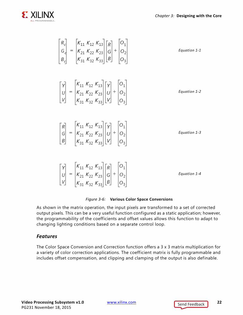
This difference can be corrected and made to more closely match the blue that is acceptable to human vision. The Color Space Converter/Correction function multiplies the pixel values by some coefficient to strengthen or weaken it, creating an effective gain. At the same time a mixture of green or red can be added to the blue channel. To express this processing mathematically, the new blue (Bc) is related to the old blue (B), red (R), and green (G) according to:
Bc = K1 x R + K2 x G + K3 x B Equation 3-4
where K1, K2, and K3 are the weights for each of the mix of red, green, and blue to the new blue.
Extending this concept, a standard 3 x 3 matrix multiplication can be applied to each of the color channels in parallel simultaneously. This is a matrix operation where the weights define a color-correction matrix. In typical applications, color-correction also contains offset compensation to ensure black [0,0,0] levels are achieved.
Send Feedback
Video Processing Subsystem v1.0 www.xilinx.com 22PG231 November 18, 2015
Chapter 3: Designing with the Core
As shown in the matrix operation, the input pixels are transformed to a set of corrected output pixels. This can be a very useful function configured as a static application; however, the programmability of the coefficients and offset values allows this function to adapt to changing lighting conditions based on a separate control loop.
Features
The Color Space Conversion and Correction function offers a 3 x 3 matrix multiplication for a variety of color correction applications. The coeff icient matrix is fully programmable and includes offset compensation, and clipping and clamping of the output is also definable.
X-Ref Target - Figure 3-6
Figure 3-6: Various Color Space Conversions
Send Feedback

Video Processing Subsystem v1.0 www.xilinx.com 23PG231 November 18, 2015
Chapter 3: Designing with the Core
The following list is a summary of the supported features:
• User programmable matrix coeff icients
• Support for RGB, YUV 4:4:4, and YUV 4:2:2
• 8, 10, 12, or 16 bits per component
• Driver API to set coeff icients for converting RGB to YUV, or vice-versa
• Driver API to set/get brightness, contrast, saturation and gain
Color Space Conversion
The primary purpose of this function is to provide color space conversion between the RGB and YUV domains. The fully programmable 3 x 3 matrix with offsets and clipping and clamping allow the support of multiple video standards.
Color Correction
This function provides support for additional color correction within a user defined window in the video frame. You can define a second coeff icient matrix to be applied only within a demo window. You also program the size and position of the demo window.
Filter Coefficients and Offsets
The coefficients are presented in 16.12 fixed point format. The 16-bit signed integer values (2’s compliment) are equivalent to real numbers in the [-8 .. 8] range.
The offset value has a width of the output data width plus 1. It is a signed integer with a range as shown in Equation 3-5.
[-2Out_Data_Width, 2Out_Data_Width-1] Equation 3-5
Output values greater than the Clip value are replaced with the Clip value. Output values smaller than the Clamp value are replaced with the Clamp value. The Clip and Clamp values have the same width as the output data width. They are unsigned integers with a range of [0 .. 2Out_Data_Width-1].
Matrix computation outputs are rounded to DATA_WIDTH bits by adding half an output LSB prior to truncation.
Chroma ResamplingThe human eye is not as receptive to chrominance (color) detail as luminance (brightness) detail. Using color-space conversion, it is possible to convert RGB into the YUV color space, where Y is Luminance information, and U and V are derived color difference signals. At normal viewing distances, there is no perceptible loss incurred by sampling the color difference signals (U and V) at a lower rate to provide a simple and effective video compression to reduce storage and transmission costs
Send Feedback

Video Processing Subsystem v1.0 www.xilinx.com 24PG231 November 18, 2015
Chapter 3: Designing with the Core
The Chroma Resampler function converts between chroma sub-sampling formats of 4:4:4, 4:2:2, and 4:2:0. There are a total of six conversions available for the three supported sub-sampling formats. Conversion is achieved using a FIR filter approach. Some conversions require filtering in only the horizontal dimension, only the vertical dimension, or both. Interpolation operations are implemented using a two-phase polyphase FIR f ilter. Decimation operations are implemented using a low-pass two-phase polyphase FIR filter to suppress chroma aliasing.
FeaturesThe Chroma Resampler function converts between different chroma sub-sampling formats. The supported formats are 4:4:4, 4:2:2, and 4:2:0. There are three different options for interpolating and decimating the video samples:
• Define a configurable f ilter with programmable coefficients for high-performance applications.
• Use the pre-defined static f ilter with power-of -two coeff icients for low-footprint applications.
• Replicate or drop pixels for minimal footprint.
The following list is a summary of the supported features:
• User programmable filter coeff icients
• 4, 6, 8, or 10 tap f ilter
• Support for RGB, YUV 4:4:4, and YUV 4:2:2, and YUV 4:2:0.
• 8, 10, 12, or 16 bits per component
Sub-sampled Video FormatsThe sub-sampling scheme is commonly expressed as a three part ratio J:a:b (for example, 4:2:2), that describes the number of luminance and chrominance samples in a conceptual region that is J pixels wide, and 2 pixels high. The parts are (in their respective order):
• J: Horizontal sampling reference (width of the conceptual region). This is usually 4.
• a: Number of chrominance samples (V, U) in the f irst row of J pixels.
• b: Number of (additional) chrominance samples (V, U) in the second row of J pixels.
To illustrate the most common sub-sampling schemes, Figure 3-7 introduces a graphical notation of sampling grid pixels.
Send Feedback

Video Processing Subsystem v1.0 www.xilinx.com 25PG231 November 18, 2015
Chapter 3: Designing with the Core
4:4:4
Similar to RGB, the 4:4:4 format is used for image capture and display purposes. U and V channels are sampled at the same rate as luminance. Hence, all pixel locations have luma and chroma data co-sited, as shown in Figure 3-8.
4:2:2
This format contains horizontally sub-sampled chroma. For every two luma samples, there is an associated pair of U and V samples. The sub-sampled chroma locations are co-sited with alternate luma samples as shown in Figure 3-9.
4:2:0
4:2:0 encoding contains horizontally and vertically sub-sampled chroma. Horizontal and vertical chroma positions are co-sited with alternate luma samples on alternate scanlines. The sampling positions are shown in Figure 3-10.
X-Ref Target - Figure 3-7
Figure 3-7: Luma, Chroma Notation
X-Ref Target - Figure 3-8
Figure 3-8: YUV 4:4:4 Format
X-Ref Target - Figure 3-9
Figure 3-9: YUV 4:2:2 Format
Send Feedback

Video Processing Subsystem v1.0 www.xilinx.com 26PG231 November 18, 2015
Chapter 3: Designing with the Core
Implementation
Between the three supported sub-sampling formats (4:4:4, 4:2:2, 4:2:0), there are six conversions available. Conversion is achieved using a FIR f ilter approach. Some require f iltering in only the horizontal dimension or only in the vertical dimension, and in some cases in both the horizontal and the vertical dimensions. These are detailed in Table 3-1 along with default f ilter information.
Three implementation options are offered for each conversion operation:
• DSP48 based f ilter with programmable coeff icients and programmable number of taps. 2D f ilters must be separable. Coefficients are in the range [-8, 8), represented in 16-bit signed, f ixed-point format with 4 integer bits and 12 fractional bits.
• Pre-defined fixed coeff icient, non-programmable f ilter with power of two coeff icients (using only shifts and additions for f iltering therefore no DSP48s are used). Default coeff icients implement linear interpolation for the interpolation and anti-aliasing low pass f ilters.
• The simplest, lowest footprint solution is to simply drop (decimation) or replicate (interpolation) samples. For down sampling, some samples are passed directly to the output, but others are dropped entirely as appropriate. For up converters, replication of the previous input sample occurs.
X-Ref Target - Figure 3-10
Figure 3-10: YUV 4:2:0 Format
Table 3-1: Chroma Resampling Configuration
Converter Filter Configuration Default FIR Size
4:4:4 to 4:2:2 Horizontal anti-aliasing 3 H Taps
4:4:4 to 4:2:0 Separable 2-D anti-aliasing 3 V Taps x 3 H Taps
4:2:2 to 4:4:4 Horizontal Interpolation 2 H Taps
4:2:2 to 4:2:0 Vertical anti-aliasing 3 V Taps
4:2:0 to 4:4:4 Separable 2-D Interpolation 2 H Taps x 2 V Taps
4:2:0 to 4:2:2 Vertical Interpolation 2 V Taps
Send Feedback

Video Processing Subsystem v1.0 www.xilinx.com 27PG231 November 18, 2015
Chapter 3: Designing with the Core
Convert 4:2:2 to 4:4:4
This conversion is a 1:2 horizontal interpolation operation, implemented using a two-phase polyphase FIR filter. One of the two output pixels is co-sited with one of the input sample. The ideal output is achieved simply by replicating this input sample.
To evaluate output pixel ox,y, the FIR filter convolves COEFk_HPHASEpx, where k is the coeff icient index, ix,y are pixels from the input image, px is the interpolation phase (0 or 1, depending on x) and [ ]Mm represents rounding with clipping at M, and clamping at m. DW is the Data Width or number of bits per video component. Ntaps is the number of f ilter taps.
Equation 3-6
In phase 1, COEF00_HPHASE1 is the coeff icient applied to the most recent input sample in the f ilter aperture. Figure 3-11 illustrates coefficient use for a four tap f ilter example, with simplif ied nomenclature a= COEF00_HPHASE1, b= COEF01_HPHASE1, c=COEF02_HPHASE1, and d= COEF03_HPHASE1.
Convert 4:4:4 to 4:2:2
This conversion is a horizontal 2:1 decimation operation, implemented using a low-pass FIR f ilter to suppress chroma aliasing. In order to evaluate output pixel ox,y, the FIR f ilter in the core convolves COEFk_HPHASE0, where k is the coeff icient index, ix,y are pixels from the input image, and [ ]Mm represents rounding with clipping at M, and clamping at m. DW is the Data Width or number of bits per video component. Ntaps is the number of f ilter taps.
Equation 3-7
In phase 0, COEF00_HPHASE0 is the coeff icient applied to the most recent input sample in the filter. Figure 3-12 illustrates coeff icient use for a 5 tap f ilter example, with simplif ied
X-Ref Target - Figure 3-11
Figure 3-11: 4:2:2 to 4:4:4 Coefficient Configuration
Send Feedback

Video Processing Subsystem v1.0 www.xilinx.com 28PG231 November 18, 2015
Chapter 3: Designing with the Core
nomenclature a= COEF00_HPHASE0, b= COEF01_HPHASE0, c= COEF02_HPHASE0, d=COEF03_HPHASE0, and e= COEF04_HPHASE0.
Convert 4:2:0 to 4:2:2
This conversion is a 1:2 vertical interpolation operation, implemented using a 2-phase polyphase FIR filter. One of the two output pixels is co-sited with one of the input sample. The ideal output is achieved simply by replicating this input sample.
To evaluate output pixel ox,y, the FIR filter in the core convolves COEFk_VPHASEpy, where k is the coeff icient index, py is the interpolation phase, ix,y are pixels from the input image, and [ ]Mm represents rounding with clipping at M, and clamping at m. DW is the Data Width or number of bits per video component. Ntaps is the number of f ilter taps.
Equation 3-8
In phase 1, COEF00_VPHASE1 is the coefficient applied to the most recent input sample in the f ilter. Figure 3-13 illustrates coeff icient use for a four tap f ilter example, with simplif ied nomenclature a= COEF00_VPHASE1, b= COEF01_VPHASE1, c= COEF02_VPHASE1, and d= COEF03_VPHASE1.
X-Ref Target - Figure 3-12
Figure 3-12: 4:4:4 to 4:2:2 Coefficient Configuration
X-Ref Target - Figure 3-13
Figure 3-13: 4:2:0 to 4:2:2 Coefficient Configuration
Send Feedback

Video Processing Subsystem v1.0 www.xilinx.com 29PG231 November 18, 2015
Chapter 3: Designing with the Core
Convert 4:2:2 to 4:2:0
This conversion is a vertical 2:1 decimation operation, implemented using a low-pass FIR f ilter to suppress chroma aliasing. In order to evaluate output pixel ox,y, the FIR filter in the core convolves COEFk_VPHASE0, where k is the coefficient index, ix,y are pixels from the input image, and [ ]Mm represents rounding with clipping at M, and clamping at m. DW is the Data Width or number of bits per video component. Ntaps is the number of f ilter taps.
Equation 3-9
In phase 0, COEF00_VPHASE0 is the coefficient applied to the most recent input sample in the f ilter. Figure 3-14 illustrates coeff icient use for a five tap f ilter example, with simplif ied nomenclature a= COEF00_VPHASE0, b= COEF01_VPHASE0, c= COEF02_VPHASE0, d= COEF03_VPHASE0, and e= COEF04_VPHASE0.
Convert 4:2:0 to 4:4:4
This conversion performs interpolation both vertically and horizontally. This is equivalent to a 2D separable f ilter implemented by cascading the 4:2:0 to 4:2:2 block and the 4:2:2 to 4:4:4 block. Quantized vertical f ilter results are f iltered by the horizontal f ilter, which in turn quantizes results back to the [0 .. 2DW-1] range. (DW is the Data Width or number of bits per video component.)
X-Ref Target - Figure 3-14
Figure 3-14: 4:2:2 to 4:2:0 Coefficient Configuration
Send Feedback

Video Processing Subsystem v1.0 www.xilinx.com 30PG231 November 18, 2015
Chapter 3: Designing with the Core
Intermediate 4:2:2 chroma values are computed using Equation 3-9. The resulting computation is shown in Equation 3-10.
Equation 3-10
Next, the values are f iltered according to Equation 3-1. The resulting computation is shown in Equation 3-11.
Equation 3-11
Convert 4:4:4 to 4:2:0
This conversion performs decimation by 2 both vertically and horizontally. This is equivalent to a 2D separable f ilter implemented by cascading the 4:4:4 to 4:2:2 block and the 4:2:2 to 4:2:0 block. Quantized horizontal f ilter results are f iltered by the vertical f ilter, which in turn quantizes results back to the [0 .. 2DW-1] range. (DW is the Data Width or number of bits per video component.)
Intermediate 4:2:2 chroma values are computed using Equation 3-2. The resulting computation is shown in Equation 3-12.
Equation 3-12
Next, these values are f iltered according to Equation 3-4. The resulting computation is shown in Equation 3-13.
Equation 3-13
X-Ref Target - Figure 3-15
X-Ref Target - Figure 3-16
ox y, ix k y,– COEFk_HPHASEpx
k 0=
Ntaps 1–
0
2DW 1–
=
Send Feedback
Video Processing Subsystem v1.0 www.xilinx.com 31PG231 November 18, 2015
Chapter 3: Designing with the Core
Resampling Filters
The upsampling and downsampling performed during the chroma format conversion is implemented with low pass f ilters for the interpolation and anti-aliasing.
The chroma resampling function offers a horizontal f ilter with a maximum of 10 taps and two phases, as well as a vertical f ilter with a maximum of 10 taps and two phases. For conversions requiring up/down sampling in both horizontal and vertical directions, 2D separable f ilters are offered.
The number of taps selected must be even (4, 6, 8, or 10). Depending on the conversion type and filter size selected, a subset of the coefficients can be used by setting the unnecessary coefficients to zero.
Each coeff icient has 16 bits in 2's complement format: 4 integer bits (one sign bit) and 12 fractional bits. The sign bit is the MSB. For example, a coefficient with a value of 1 is represented with this bit vector
[0001000000000000].
The coefficients should sum to exactly 1 to achieve unity gain. If they sum to less than 1, some loss of dynamic range is observed.
Computation Bit Width Growth
Full precision (DATA_WIDTH+16+log2(NTaps) bits) is maintained during the horizontal and/or vertical FIR convolution operation.
FIR f ilter outputs are rounded to DATA_WIDTH bits by adding half an output LSB in the full precision domain prior to truncation. Clipping and clamping of the output data prevents overflows and underflows. Data is clipped and clamped at 2DATA_WIDTH-1 and 0.
Edge Padding
The edge pixels of images are replicated prior to filtering to avoid image artifacts.
ClockingThe AXI Streaming, AXI Memory, and AXI Lite interfaces can be run at their own clock rate. Therefore, three seperate clock interfaces are provided named aclk_axis, aclk_axi_mm, and aclk_ctrl, respectively.
Send Feedback

Video Processing Subsystem v1.0 www.xilinx.com 32PG231 November 18, 2015
Chapter 3: Designing with the Core
ResetsThe aresetn_ctrl signal is the active-Low reset input signal of the IP. The reset signal must be synchronous to the aclk_ctrl signal. Each time this reset is asserted, it should be asserted for a minimum of 16 clock cycles of the slowest clock. All registers are reset to power-on conditions; all queues are flushed; all internal logic returned to power-on conditions.
The aresetn_io_axis signal is an outgoing signal that can be used to hold IPs in reset when the video processing subsystem IP is not ready to consume data on the streaming input.This reset signal is synchronous to the aclk_axis signal.
Send Feedback

Video Processing Subsystem v1.0 www.xilinx.com 33PG231 November 18, 2015
Chapter 4
Design Flow StepsThis chapter describes customizing and generating the core, constraining the core, and the simulation, synthesis and implementation steps that are specific to this IP core. More detailed information about the standard Vivado® design flows and the IP integrator can be found in the following Vivado Design Suite user guides:
• Vivado Design Suite User Guide: Designing IP Subsystems using IP Integrator (UG994) [Ref 1]
• Vivado Design Suite User Guide: Designing with IP (UG896) [Ref 2]
• Vivado Design Suite User Guide: Getting Started (UG910) [Ref 3]
• Vivado Design Suite User Guide: Logic Simulation (UG900) [Ref 4]
Customizing and Generating the CoreThis section includes information about using Xilinx tools to customize and generate the core in the Vivado Design Suite.
The Video Processing Subsystem can only be added to a Vivado IP integrator block design in the Vivado Design Suite. For more detailed information on customizing and generating the core in the Vivado IP integrator, see the Vivado Design Suite User Guide: Designing IP Subsystems using IP Integrator (UG994) [Ref 1]. IP integrator might auto-compute certain configuration values when validating or generating the design. To check whether the values do change, see the description of the parameter in this chapter. To view the parameter value, run the validate_bd_design command in the Tcl console.
You can customize the IP for use in your design by specifying values for the various parameters associated with the IP core using the following steps:
1. In the Flow Navigator, click on Create Block Diagram or Open Block Design under the IP Integrator heading.
2. Right click in the diagram and select Add IP.
A searchable IP catalog opens. You can also add IP by clicking on the Add IP button on the left side of the IP Integrator Block Design canvas.
Send Feedback
Video Processing Subsystem v1.0 www.xilinx.com 34PG231 November 18, 2015
Chapter 4: Design Flow Steps
3. Click on the IP name and press the Enter key on your keyboard or double click on the IP name.
4. Double-click the selected IP block or select the Customize Block command from the right-click menu.
For details, see the Vivado Design Suite User Guide: Designing with IP (UG896) [Ref 2] and the Vivado Design Suite User Guide: Getting Started (UG910) [Ref 3].
Note: Figures in this chapter are illustrations of the Vivado Integrated Design Environment (IDE). The layout depicted here might vary from the current version.
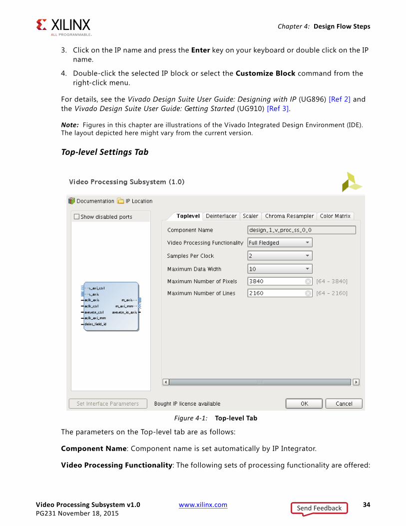
Top-level Settings Tab
The parameters on the Top-level tab are as follows:
Component Name: Component name is set automatically by IP Integrator.
Video Processing Functionality: The following sets of processing functionality are offered:
X-Ref Target - Figure 4-1
Figure 4-1: Top-level Tab
Send Feedback

Video Processing Subsystem v1.0 www.xilinx.com 35PG231 November 18, 2015
Chapter 4: Design Flow Steps
° Scaler Only: The subsystem is configured to perform only the scaling function.
° Full Fledged: The full-fledged design performs deinterlacing, scaling, color space conversion and correction, chroma resampling, and frame rate conversion (drop/repeat).
Samples Per Clock : Select 1, 2, or 4 pixel wide interface.
Maximum Data Width: Select 8, 10, 12, or 16 bit color depth.
Maximum Number of Pixels: Specify the maximum number of pixels per scanline. Permitted values are from 64 to 4096. Specifying this value is necessary to establish the depth of internal line buffers. Using a tight upper-bound results in optimal block RAM usage. The active frame size can be programmed during run-time via the AXI4-Lite interface and driver API. The number of active columns must be less than or equal to the Maximum Number of Pixels.
Maximum Number of Lines: Specify the maximum number of scanlines per frame. Permitted values are from 64 to 2160. The active frame size can be programmed during run-time via the AXI4-Lite interface and driver API. The number of active rows must be less than or equal to the Maximum Number of Lines.
Deinterlacer Settings
The deinterlacer does not have any additional build-time configuration options. See Driver in Appendix C for information on run-time configurability.
Send Feedback

Video Processing Subsystem v1.0 www.xilinx.com 36PG231 November 18, 2015
Chapter 4: Design Flow Steps
Scaler Settings
The parameters on the Scaler tab are as follows:
Algorithm: The Scaler comes in three different quality levels each at different levels of resource usage.
° Bilinear - Bilinear scaling uses bilinear interpolation to calculate pixels.
° Bicubic - Bicubic scaling is a little bit more demanding compared to bilinear scaling, and produces smoother pictures with less artifacts.
° Polyphase - The picture quality (and resource usage) of a polyphase scaler depends largely on the number of f ilter taps used and number of f ilter phases used.
Polyphase Filter Control: When polyphase filtering is selected, the horizontal and vertical taps and phases are defined here.
° Horizontal Taps – Select 6, 8, 10, or 12 horizontal f ilter taps.
° Vertical Taps – Select 6, 8, 10, or 12 vertical f ilter taps.
° Horizontal Phases – Only 64 phases is currently supported.
° Vertical Phases – Only 64 phases is currently supported.
X-Ref Target - Figure 4-2
Figure 4-2: Scaler Tab
Send Feedback
Video Processing Subsystem v1.0 www.xilinx.com 37PG231 November 18, 2015
Chapter 4: Design Flow Steps
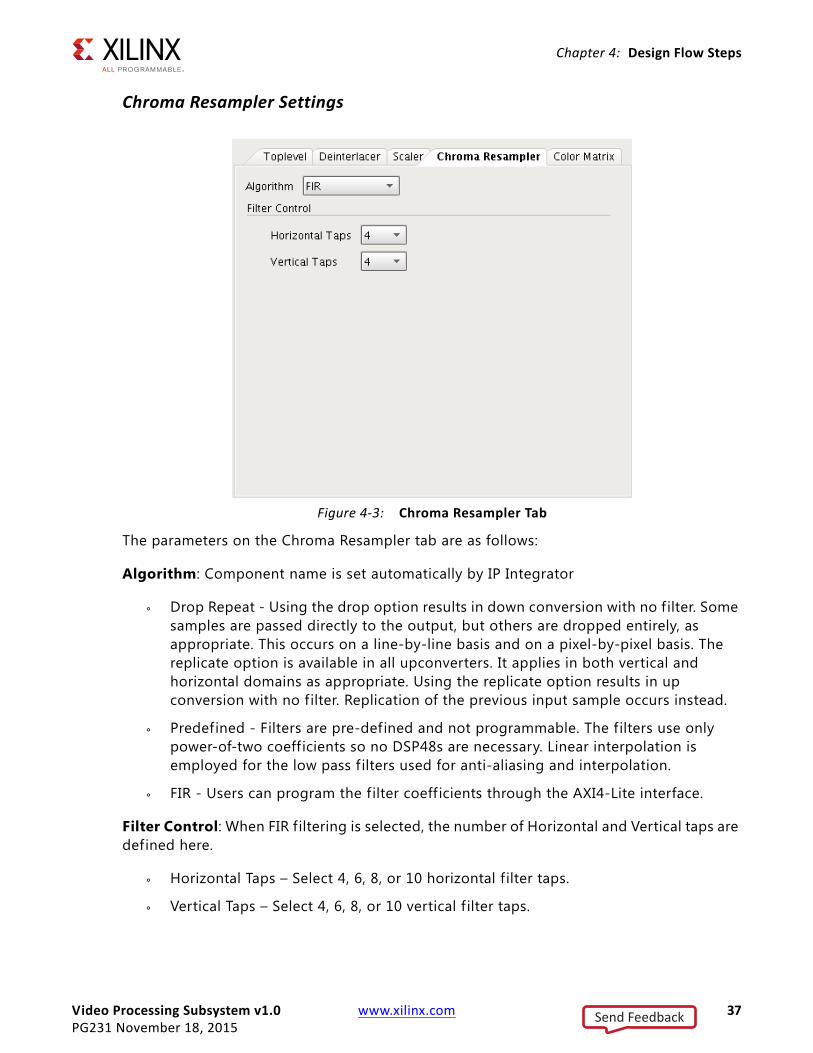
Chroma Resampler Settings
The parameters on the Chroma Resampler tab are as follows:
Algorithm: Component name is set automatically by IP Integrator
° Drop Repeat - Using the drop option results in down conversion with no f ilter. Some samples are passed directly to the output, but others are dropped entirely, as appropriate. This occurs on a line-by-line basis and on a pixel-by-pixel basis. The replicate option is available in all upconverters. It applies in both vertical and horizontal domains as appropriate. Using the replicate option results in up conversion with no f ilter. Replication of the previous input sample occurs instead.
° Predefined - Filters are pre-defined and not programmable. The filters use only power-of-two coefficients so no DSP48s are necessary. Linear interpolation is employed for the low pass f ilters used for anti-aliasing and interpolation.
° FIR - Users can program the filter coeff icients through the AXI4-Lite interface.
Filter Control: When FIR filtering is selected, the number of Horizontal and Vertical taps are defined here.
° Horizontal Taps – Select 4, 6, 8, or 10 horizontal f ilter taps.
° Vertical Taps – Select 4, 6, 8, or 10 vertical f ilter taps.
X-Ref Target - Figure 4-3
Figure 4-3: Chroma Resampler Tab
Send Feedback

Video Processing Subsystem v1.0 www.xilinx.com 38PG231 November 18, 2015
Chapter 4: Design Flow Steps
Color Matrix Settings
The color matrix does not have any additional build-time configuration options. See Driver in Appendix C for information on run-time configurability.
User ParametersTable 4-1 shows the relationship between the f ields in the Vivado IDE and the User Parameters (which can be viewed in the Tcl Console).
Table 4-1: Vivado IDE Parameter to User Parameter RelationshipVivado IDE Parameter/Value(1) User Parameter/Value(1) Default Value
Top LevelAlgorithm C_SCALER_ALGORITHM Polyphase
Bilinear 0
Bicubic 1
Polyphase 2
Video Processing Functionality C_TOPOLOGY Scaler Only
Scaler Only 0
Full Fledged 1
Samples Per Clock C_SAMPLES_PER_CLK 2
Maximum Data Width C_MAX_DATA_WIDTH 10
Maximum Number of Pixels C_MAX_COLS 3840
Maximum Number of Lines C_MAX_ROWS 2160
ScalerHorizontal Taps C_H_SCALER_TAPS 6
Vertical Taps C_V_SCALER_TAPS 6
Horizontal Phases C_H_SCALER_PHASES 64
Vertical Phases C_V_SCALER_PHASES 64
Chroma ResamplerAlgorithm C_CHROMA_ALGORITHM FIR
Drop Repeat 0
Predefined 1
FIR 2
Horizontal Taps C_H_CHROMA_TAPS 4
Vertical Taps C_V_CHROMA_TAPS 4
Notes: 1. Parameter values are listed in the table where the Vivado IDE parameter value differs from the user parameter
value. Such values are shown in this table as indented below the associated parameter.
Send Feedback

Video Processing Subsystem v1.0 www.xilinx.com 39PG231 November 18, 2015
Chapter 4: Design Flow Steps
Output GenerationFor details, see the Vivado Design Suite User Guide: Designing with IP (UG896) [Ref 2].
Constraining the CoreThis section contains information about constraining the core in the Vivado Design Suite.
Required ConstraintsThe only constraints required are clock frequency constraints for the AXI4-Stream video interfaces clock, aclk_axis, AXI4-Lite control interface clock, aclk_ctrl, and memory subsystem clock, aclk_axi_mm. Paths from AXI4-Lite signals should be constrained with a set_false_path, causing setup and hold checks to be ignored for AXI4-Lite signals. These constraints are provided in the XDC constraints f iles included with the IP.
Device, Package, and Speed Grade SelectionsThis section is not applicable for this IP core.
Clock FrequenciesThis section is not applicable for this IP core.
Clock ManagementThis section is not applicable for this IP core.
Clock PlacementThis section is not applicable for this IP core.
BankingThis section is not applicable for this IP core.
Transceiver PlacementThis section is not applicable for this IP core.
Send Feedback
Video Processing Subsystem v1.0 www.xilinx.com 40PG231 November 18, 2015
Chapter 4: Design Flow Steps
I/O Standard and PlacementThis section is not applicable for this IP core.
SimulationSimulation of this core is not supported.
Synthesis and ImplementationFor details about synthesis and implementation, see the Vivado Design Suite User Guide: Designing with IP (UG896) [Ref 2].
Send Feedback

Video Processing Subsystem v1.0 www.xilinx.com 41PG231 November 18, 2015
Chapter 5
Detailed Example DesignAn IP Integrator example design is provided to demonstrate the Video Processing Subsystem capabilities. The Scaler-only design showcases the video subsystem in a Scaler-only configuration. The full-fledged design adds deinterlacing, color space conversion and correction, chroma resampling, and frame rate conversion (drop/repeat).
IMPORTANT: The example project is only available on Xilinx KC705 evaluation board.
To open the example project, perform the following:
1. Add the IP to an IP Integrator Block Design canvas.
2. After the IP has been instantiated in the block design, double-click on it to customize it.
3. Right-click the selected IP block and select Open IP Example Design from the menu.
4. In the Open IP Example Design window, select example project directory and click OK.
A new session of the Vivado IDE opens that shows the example design in the Design Sources window.
Full-fledged Video Processing DesignFigure 5-1 shows the top level block diagram. In the video path is a video test pattern generator and an AXI4-Stream to Video Out core. Furthermore, a MicroBlaze™ processor is controlling the IPs, and a memory interconnect with MIG are interfacing with external DDR.
Send Feedback

Video Processing Subsystem v1.0 www.xilinx.com 42PG231 November 18, 2015
Chapter 5: Detailed Example Design
Scaler-only Video Processing DesignFigure 5-2 shows the top level block diagram of the Scaler-only design.
Video PathA video test pattern generator feeds into the Video Processing Subsystem IP. The output of the video processing IP subsystem is connected to the AXI4-Stream to Video Out IP.
X-Ref Target - Figure 5-1
Figure 5-1: Top-level Full-fledged Video Processing Design
X-Ref Target - Figure 5-2
Figure 5-2: Top-level Scaler-only Video Processing Design
Send Feedback

Video Processing Subsystem v1.0 www.xilinx.com 43PG231 November 18, 2015
Chapter 5: Detailed Example Design
Memory SubsystemThe memory subsystem in the full-fledged design consists of an AXI-MM interconnect that is a 3:1 cross-bar that feeds into the MIG. The 3 ports feeding into the cross bar are the data and instruction cache ports from the Microblaze, and the memory port of the video processing IP subsystem. For the Scaler-only design, the interconnect is a 2:1 cross bar.
Processor SubsystemA MicroBlaze processor is used for controlling the IPs. The example design uses the default configuration which is not optimized for performance as CPU load is not critical. The MicroBlaze has 8KB data and instruction caches added. The MicroBlaze processor is being run at 100 MHz clock speed.
ClockingThe Video Processing Subsystem IP uses three clocks that are derived through a clock generator from the 200 MHz system clock that is available on the Kintex-7 KC705 board. The memory subsystem is running at this system clock at 200 MHz. This system clock feeds into the clock wizard IP, which derives a 300 MHz and 100 MHz clock at the output. The 300 MHz clock drives the AXI4-Stream video interfaces. The 100 MHz clock drives the AXI4-Lite control interface, and also drives the MicroBlaze processor.
Example Design SoftwareThe synthsizable example design requires both Vivado and Xilinx SDK tools.
The first step is to run synthesis, implementation and bitstream generation in Vivado. After all those steps are done, select File -> Export -> Export Hardware. In the window, select Include bitstream, select an export directory and click OK.
The remaining work is performed in Xilinx SDK tool. The example design f ile can be found at SDK directory:
(<install_directory>/2015.3/data/embeddedsw/XilinxProcessorIPLib/drivers/ vprocss_v1_0/examples/
Example application design source f iles (contained within "examples" folder) are tightly coupled with the example design available in Vivado Catalog.
vpss_example.tcl automates the process of generating the downloadable bit and elf f iles from the provided example hdf f ile.
To run the provided Tcl script:
1. Copy the exported example design hdf file in the "examples" directory of the driver
2. Launch the Xilinx Software Command-Line Tool (xsct) terminal
Send Feedback

Video Processing Subsystem v1.0 www.xilinx.com 44PG231 November 18, 2015
Chapter 5: Detailed Example Design
3. cd into the examples directory
4. Source the tcl f ile
xsct%>source vpss_example.tcl
5. Execute the script
xsct%>vpss_example <hdf_file_name.hdf>
The Tcl script performs the following:
• Create workspace
• Create HW project
• Create BSP
• Create Application Project
• Build BSP and Application Project
After the process is complete, the required f iles are available in:
bit file -> vpss_example.sdk/vpss_example_hw_platform folderelf file -> vpss_example.sdk/vpss_example_design/{Debug/Release} folder
Next, perform the following steps to run the software application:
IMPORTANT: To do so, make sure that the hardware is powered on and a Digilent Cable or an USB Platform Cable is connected to the host PC. Also, ensure that a USB cable is connected to the UART port of the KC705 board.
1. Launch SDK.
2. Set workspace to vpss_example.sdk folder in prompted window. The SDK project opens automatically. (If a welcome page shows up, close that page.)
3. Download the bitstream into the FPGA by selecting Xilinx Tools > Program FPGA. The Program FPGA dialog box opens.
4. Ensure that the Bitstream field shows the bitstream file generated by Tcl script, and then click Program.
Note: The DONE LED on the board turns green if the programming is successful.
5. A terminal program (HyperTerminal or PuTTY) is needed for UART communication. Open the program, choose appropriate port, set baud rate to 9600 and establish Serial port connection.
6. Select and right-click the application vpss_example_design in Project_Explorer panel.
7. Select Run As > Launch on Hardware (GDB).
8. Select Binaries and Qualif ier in window and click OK.
Send Feedback
Video Processing Subsystem v1.0 www.xilinx.com 45PG231 November 18, 2015
Chapter 5: Detailed Example Design
The example design test result are shown in terminal program.
For more information, visit www.xilinx.com/tools/sdk.htm.
When executed on the board, the example application determines the Video Processing Subsystem topology and sets the input and output stream configuration accordingly. The test pattern generator IP is used to generate the input stream. Video Lock Monitor IP then monitors the output of the subsystem (to vidout) to determine if lock is achieved and present the status (Pass/Fail) on the terminal.
Send Feedback

Video Processing Subsystem v1.0 www.xilinx.com 46PG231 November 18, 2015
Appendix A
Migrating and UpgradingThis appendix contains information about upgrading to a more recent version of the IP core.
Upgrading in the Vivado Design SuiteThis section is not applicable for the f irst release of the core.
Send Feedback

Video Processing Subsystem v1.0 www.xilinx.com 47PG231 November 18, 2015
Appendix B
DebuggingThis appendix includes details about resources available on the Xilinx Support website and debugging tools.
TIP: If the IP generation halts with an error, there might be a license issue. See License Checkers in Chapter 1 for more details.
Finding Help on Xilinx.comTo help in the design and debug process when using the Video Processing Subsystem, the Xilinx Support web page contains key resources such as product documentation, release notes, answer records, information about known issues, and links for obtaining further product support.
DocumentationThis product guide is the main document associated with the Video Processing Subsystem. This guide, along with documentation related to all products that aid in the design process, can be found on the Xilinx Support web page or by using the Xilinx Documentation Navigator.
Download the Xilinx Documentation Navigator from the Downloads page. For more information about this tool and the features available, open the online help after installation.
Solution CentersSee the Xilinx Solution Centers for support on devices, software tools, and intellectual property at all stages of the design cycle. Topics include design assistance, advisories, and troubleshooting tips.
The Solution Center specif ic to the Video Processing Subsystem core is listed below.
• Xilinx Multimedia, Video and Imaging Solution Center
Send Feedback

Video Processing Subsystem v1.0 www.xilinx.com 48PG231 November 18, 2015
Appendix B: Debugging
Answer Records Answer Records include information about commonly encountered problems, helpful information on how to resolve these problems, and any known issues with a Xilinx product. Answer Records are created and maintained daily ensuring that users have access to the most accurate information available.
Answer Records for this core can be located by using the Search Support box on the main Xilinx support web page. To maximize your search results, use proper keywords such as
• Product name
• Tool message(s)
• Summary of the issue encountered
A filter search is available after results are returned to further target the results.
Master Answer Record for the Video Processing Subsystem
AR: 65449
Technical SupportXilinx provides technical support at the Xilinx Support web page for this LogiCORE™ IP product when used as described in the product documentation. Xilinx cannot guarantee timing, functionality, or support if you do any of the following:
• Implement the solution in devices that are not defined in the documentation.
• Customize the solution beyond that allowed in the product documentation.
• Change any section of the design labeled DO NOT MODIFY.
To contact Xilinx Technical Support, navigate to the Xilinx Support web page.
Debug ToolsThere are many tools available to address Video Processing Subsystem design issues. It is important to know which tools are useful for debugging various situations.
Send Feedback

Video Processing Subsystem v1.0 www.xilinx.com 49PG231 November 18, 2015
Appendix B: Debugging
Vivado Design Suite Debug FeatureThe Vivado® Design Suite debug feature inserts logic analyzer and virtual I/O cores directly into your design. The debug feature also allows you to set trigger conditions to capture application and integrated block port signals in hardware. Captured signals can then be analyzed. This feature in the Vivado IDE is used for logic debugging and validation of a design running in Xilinx devices.
The Vivado logic analyzer is used with the logic debug IP cores, including:
• ILA 2.0 (and later versions)
• VIO 2.0 (and later versions)
See the Vivado Design Suite User Guide: Programming and Debugging (UG908) [Ref 6].
Reference BoardsVarious Xilinx development boards support the Video Processing Subsystem. These boards can be used to prototype designs and establish that the core can communicate with the system. The Video Processing Subsystem offers an Example Design which Xilinx recommends for getting acquainted with the core.
• 7 series FPGA evaluation boards
° KC705
Simulation DebugSimulation of this core is not supported.
Hardware DebugHardware issues can range from link bring-up to problems seen after hours of testing. This section provides debug steps for common issues. Vivado Lab Edition is a valuable resource to use in hardware debug. The signal names mentioned in the following individual sections can be probed using Vivado Lab Edition for debugging the specif ic problems.
General ChecksEnsure that all the timing constraints for the core were properly incorporated from the example design and that all constraints were met during implementation.
Send Feedback

Video Processing Subsystem v1.0 www.xilinx.com 50PG231 November 18, 2015
Appendix B: Debugging
• Does it work in post-place and route timing simulation? If problems are seen in hardware but not in timing simulation, this could indicate a PCB issue. Ensure that all clock sources are active and clean.
• If using MMCMs in the design, ensure that all MMCMs have obtained lock by monitoring the locked port.
• If your outputs go to 0, check your licensing.
Interface Debug
AXI4-Lite InterfacesRead from a register that does not have all 0s as a default to verify that the interface is functional. Output s_axi_arready asserts when the read address is valid, and output s_axi_rvalid asserts when the read data/response is valid. If the interface is unresponsive, ensure that the following conditions are met:
• The s_axi_aclk and aclk inputs are connected and toggling.
• The interface is not being held in reset, and s_axi_areset is an active-Low reset.
• The interface is enabled, and s_axi_aclken is active-High (if used).
• The main core clocks are toggling and that the enables are also asserted.
• If the simulation has been run, verify in simulation and/or a Vivado Lab Edition capture that the waveform is correct for accessing the AXI4-Lite interface.
AXI4-Stream InterfacesIf data is not being transmitted or received, check the following conditions:
• If transmit <interface_name>_tready is stuck Low following the <interface_name>_tvalid input being asserted, the core cannot send data.
• If the receive <interface_name>_tvalid is stuck Low, the core is not receiving data.
• Check that the aclk inputs are connected and toggling.
• Check that the AXI4-Stream waveforms are being followed.
• Check core configuration.
Send Feedback

Video Processing Subsystem v1.0 www.xilinx.com 51PG231 November 18, 2015
Appendix C
Application Software Development
DriverThe Video Processing Subsystem driver abstracts the included video processing elements and presents the processing chain as a black-box. It shields you from the internal workings of included subcores and thus provides an out-of-the-box solution for video
The subsystem driver is a bare-metal driver. It dynamically manages the data and control flow through the processing elements, based on the input/output stream configuration set at run time. Internally, it relies on included subcore layer 1 drivers to configure the IP hardware block and layer 2 drivers to provide an abstracted view of the feature set provided by each subcore.
DependenciesA video common driver is delivered as part of the SDK. Most video IPs have master/slave AXI4-Stream interfaces so the concept of Video Streams as an interface parameter for drivers for such cores was introduced.
The video_common_v2_0 defines the following features:
• Enumerations for video specif ic details like color format, color depth, frame rate, etc.
• Video stream, Video timing and video window data types.
• Video Mode Table with pre-defined resolutions and their timing details.
• Utility APIs that can access data from the mode table and work with stream data types.
ArchitectureThe subsystem driver provides an easy-to-use, well-defined API to help integrate the subsystem in an application without having to understand the underlying complexity of configuring each and every subcore.
Send Feedback

Video Processing Subsystem v1.0 www.xilinx.com 52PG231 November 18, 2015
Appendix C: Application Software Development
Subsystem driver consists of the following:
• Subsystem layer: Controls the data/control flow of AXI4-Stream through the processing cores. It uses support functions to examine the input and output stream properties and make appropriate decision to implement the determined use case.
• Subcore drivers: Every included subcore has a driver associated with it and provides 2 layers of abstraction
° Layer-1: Implements API's to peek/poke IP registers at HW level.
° Layer-2: Implements feature set to abstract core functionality.
For example, the color space conversion IP at the core level contains a 3 x 3 coeff icient matrix which must be manipulated to do the required conversion, for example RGB to YUV.
• Layer-1 provides APIs to read/write these 3 x 3 coefficient registers. You are responsible for computing the required coefficient values and program the specific registers.
• Layer-2 implements the feature set that can be built upon layer-1 and is much easier to use:
° API to convert RGB to YUV or vice-versa.
° API to set/get brightness, contrast, saturation and gain.
° Auto translation between user setting of 0-100 to IP offered range.
Figure C-1 shows the Video Processing Subsystem architecture.
X-Ref Target - Figure C-1
Figure C-1: Subsystem Driver Architecture
Send Feedback

Video Processing Subsystem v1.0 www.xilinx.com 53PG231 November 18, 2015
Appendix C: Application Software Development
PrerequisitesFor full-fledged topology, the subsystem requires external memory to store video buffers. You must specify the DDR address for the buffer storage. The API to use is:
void XVprocSs_SetFrameBufBaseaddr(XVprocSs *InstancePtr, u32 addr);
There is no similar requirement for the Scaler-only topology.
UsageThe subsystem driver itself is not an active driver and relies on application software to make use of the provided APIs to configure it. Application software is responsible to monitor the system for external inputs and communicate changes to input/output stream properties to the subsystem through provided API's, and trigger the subsystem auto reconfiguration process.
To integrate and use the Video Processing Subsystem driver in a user application, the following steps must be followed:
1. Include the subsystem header file xvprocss.h that defines the subsystem object.
2. Declare an instance of the subsystem object in the application code:
XVprocSs VprocInst;
3. Initialize system peripherals (timer, interrupt controller, UART, etc.) in the application.
4. If delay routine is defined at application level using a timer, this must be registered with the subsystem:
void XVprocSs_SetUserTimerHandler(XVprocSs *InstancePtr, XVidC_DelayHandler CallbackFunc, void *CallbackRef);
If the application is not using the timing peripheral to implement the timeouts, skip this step. The Subsystem driver internally uses the platform-specific delay handler.
5. Initialize Video Processing Subsystem at Power-On.
int XVprocSs_CfgInitialize(XVprocSs *InstancePtr, XVprocSs_Confg *CfgPtr, u32 EffectiveAddr);
Accesses the HW configuration determines the included subcores and initializes them to the power on default. The input and output stream resolution is set to 1080p at 60 Hz, RGB, and color depth is 10-bit. Finally all the cores are reset and the subsystem Ready flag is set.
6. Configure subsystem:
Send Feedback

Video Processing Subsystem v1.0 www.xilinx.com 54PG231 November 18, 2015
Appendix C: Application Software Development
int XVprocSs_ConfigureSubsystem(XVprocss *InstancePtr);
This API is the entry point and trigger mechanism for the subsystem processing control flow. It examines the input and output stream properties and validates them against the supported feature set. If the use case is supported, the driver determines the subcores required to implement the use case, builds a data flow network, configures cores in the network, and starts the video pipe.
Now, the subsystem is ready for use and the application software monitors changes in the system input or output and communicates those changes to the video subsystem.
Send Feedback
Video Processing Subsystem v1.0 www.xilinx.com 55PG231 November 18, 2015
Appendix D
Additional Resources and Legal Notices
Xilinx ResourcesFor support resources such as Answers, Documentation, Downloads, and Forums, see Xilinx Support.
ReferencesThese documents provide supplemental material useful with this product guide:
1. Vivado® Design Suite User Guide: Designing IP Subsystems using IP Integrator (UG994)
2. Vivado Design Suite User Guide: Designing with IP (UG896)
3. Vivado Design Suite User Guide: Getting Started (UG910)
4. Vivado Design Suite User Guide: Logic Simulation (UG900)
5. ISE to Vivado Design Suite Migration Guide (UG911)
6. Vivado Design Suite User Guide: Programming and Debugging (UG908)
7. Vivado Design Suite User Guide: Implementation (UG904)
8. AXI Reference Guide (UG1037)
Send Feedback

Video Processing Subsystem v1.0 www.xilinx.com 56PG231 November 18, 2015
Appendix D: Additional Resources and Legal Notices
Revision HistoryThe following table shows the revision history for this document.
Please Read: Important Legal NoticesThe information disclosed to you hereunder (the “Materials”) is provided solely for the selection and use of Xilinx products. To the maximum extent permitted by applicable law: (1) Materials are made available "AS IS" and with all faults, Xilinx hereby DISCLAIMS ALL WARRANTIES AND CONDITIONS, EXPRESS, IMPLIED, OR STATUTORY, INCLUDING BUT NOT LIMITED TO WARRANTIES OF MERCHANTABILITY, NON-INFRINGEMENT, OR FITNESS FOR ANY PARTICULAR PURPOSE; and (2) Xilinx shall not be liable (whether in contract or tort, including negligence, or under any other theory of liability) for any loss or damage of any kind or nature related to, arising under, or in connection with, the Materials (including your use of the Materials), including for any direct, indirect, special, incidental, or consequential loss or damage (including loss of data, profits, goodwill, or any type of loss or damage suffered as a result of any action brought by a third party) even if such damage or loss was reasonably foreseeable or Xilinx had been advised of the possibility of the same. Xilinx assumes no obligation to correct any errors contained in the Materials or to notify you of updates to the Materials or to product specifications. You may not reproduce, modify, distribute, or publicly display the Materials without prior written consent. Certain products are subject to the terms and conditions of Xilinx’s limited warranty, please refer to Xilinx’s Terms of Sale which can be viewed at http://www.xilinx.com/legal.htm#tos; IP cores may be subject to warranty and support terms contained in a license issued to you by Xilinx. Xilinx products are not designed or intended to be fail-safe or for use in any application requiring fail-safe performance; you assume sole risk and liability for use of Xilinx products in such critical applications, please refer to Xilinx’s Terms of Sale which can be viewed at http://www.xilinx.com/legal.htm#tos.
Date Version Revision
11/18/2015 1.0 Added support for UltraScale+ devices.
10/19/2015 1.0 Initial Xilinx release.
Send Feedback