Embed Size (px)
Citation preview
VFP9-S™ Vector Floating-pointCoprocessor
r0p2
Technical Reference Manual
Copyright © 2002, 2003 ARM Limited. All rights reserved.ARM DDI 0238B

VFP9-S r0p2 Vector Floating-point CoprocessorTechnical Reference Manual
Copyright © 2002, 2003 ARM Limited. All rights reserved.
Release Information
Proprietary Notice
Words and logos marked with ® or ™ are registered trademarks or trademarks of ARM Limited in the EU and other countries, except as otherwise stated below in this proprietary notice. Other brands and names mentioned herein may be the trademarks of their respective owners.
Neither the whole nor any part of the information contained in, or the product described in, this document may be adapted or reproduced in any material form except with the prior written permission of the copyright holder.
The product described in this document is subject to continuous developments and improvements. All particulars of the product and its use contained in this document are given by ARM Limited in good faith. However, all warranties implied or expressed, including but not limited to implied warranties of merchantability, or fitness for purpose, are excluded.
This document is intended only to assist the reader in the use of the product. ARM Limited shall not be liable for any loss or damage arising from the use of any information in this document, or any error or omission in such information, or any incorrect use of the product.
Confidentiality Status
This document is Open Access. This document has no restriction on distribution.
Product Status
The information in this document is final (information on a developed product).
Web Address
http://www.arm.com
Change history
Date Issue Change
10 April, 2002 A First release
20 October, 2003 B First release for r0p2
ii Copyright © 2002, 2003 ARM Limited. All rights reserved. ARM DDI 0238B
ContentsVFP9-S r0p2 Vector Floating-point Coprocessor Technical Reference Manual
PrefaceAbout this manual ......................................................................................... xiiFeedback ...................................................................................................... xv
Chapter 1 Introduction1.1 About the VFP9-S coprocessor ................................................................. 1-21.2 Applications ................................................................................................. 1-31.3 Coprocessor interface ................................................................................. 1-41.4 VFP9-S pipelines ........................................................................................ 1-51.5 Modes of operation ................................................................................... 1-121.6 Short vector instructions ........................................................................... 1-151.7 Using CPBURST ....................................................................................... 1-161.8 Parallel execution of instructions ............................................................... 1-171.9 VFP9-S treatment of branch instructions .................................................. 1-181.10 Writing optimal VFP9-S code .................................................................... 1-191.11 Clocking .................................................................................................... 1-201.12 Testing ...................................................................................................... 1-211.13 Silicon revision information ....................................................................... 1-22
ARM DDI 0238B Copyright © 2002, 2003 ARM Limited. All rights reserved. iii
Contents
Chapter 2 Register File2.1 About the register file .................................................................................. 2-22.2 Register file internal formats ....................................................................... 2-32.3 Decoding the register file ............................................................................ 2-52.4 Loading operands from ARM registers ....................................................... 2-62.5 Maintaining consistency in register precision ............................................. 2-82.6 Data transfer between memory and VFP9-S registers ............................... 2-92.7 Access to register banks in CDP operations ............................................ 2-11
Chapter 3 Programmer’s Model3.1 About the programmer’s model .................................................................. 3-23.2 Compliance with the IEEE 754 standard .................................................... 3-33.3 ARMv5TE coprocessor extensions ............................................................ 3-93.4 VFP9-S system control and status registers ............................................ 3-15
Chapter 4 Instruction Execution4.1 About instruction execution ........................................................................ 4-24.2 Serializing instructions ................................................................................ 4-34.3 Interrupting the VFP9-S coprocessor ......................................................... 4-44.4 Forwarding .................................................................................................. 4-54.5 Hazards ...................................................................................................... 4-74.6 Operation of the scoreboard ....................................................................... 4-84.7 Parallel execution ..................................................................................... 4-234.8 Execution timing ....................................................................................... 4-26
Chapter 5 Exception Handling5.1 About exception processing ....................................................................... 5-25.2 Support code .............................................................................................. 5-35.3 Illegal instructions ....................................................................................... 5-65.4 Determination of the trigger instruction ....................................................... 5-75.5 Input Subnormal exception ....................................................................... 5-125.6 Invalid Operation exception ...................................................................... 5-135.7 Division-by-Zero exception ....................................................................... 5-165.8 Overflow exception ................................................................................... 5-175.9 Underflow exception ................................................................................. 5-195.10 Inexact exception ...................................................................................... 5-215.11 Input exceptions ....................................................................................... 5-225.12 Arithmetic exceptions ............................................................................... 5-23
Chapter 6 Design for Test6.1 VFP9-S coprocessor .................................................................................. 6-26.2 VFP9-S test wrapper .................................................................................. 6-36.3 Test Pins ..................................................................................................... 6-6
iv Copyright © 2002, 2003 ARM Limited. All rights reserved. ARM DDI 0238B

Contents
Chapter 7 Validating external connections7.1 About using the test wrapper ...................................................................... 7-27.2 Validation .................................................................................................... 7-3
Glossary
Index
ARM DDI 0238B Copyright © 2002, 2003 ARM Limited. All rights reserved. v

Contents
vi Copyright © 2002, 2003 ARM Limited. All rights reserved. ARM DDI 0238B

List of TablesVFP9-S r0p2 Vector Floating-point Coprocessor Technical Reference Manual
Change history .............................................................................................................. iiTable 2-1 VFP9-S MCR instructions ......................................................................................... 2-6Table 2-2 VFP9-S MRC instructions ......................................................................................... 2-6Table 2-3 VFP9-S MCRR instructions ....................................................................................... 2-7Table 2-4 VFP9-S MRRC instructions ....................................................................................... 2-7Table 2-5 Single-precision data memory images and byte addresses ...................................... 2-9Table 2-6 Double-precision data memory images and byte addresses .................................. 2-10Table 2-7 Single-precision three-operand register usage ....................................................... 2-14Table 2-8 Single-precision two-operand register usage .......................................................... 2-15Table 2-9 Double-precision three-operand register usage ...................................................... 2-15Table 2-10 Double-precision two-operand register usage ........................................................ 2-15Table 3-1 Default NaN values ................................................................................................... 3-5Table 3-2 Access to control registers ...................................................................................... 3-16Table 3-3 Encoding of the VFP9-S floating-point system ID register ...................................... 3-17Table 3-4 Encoding of floating-point status and control register ............................................. 3-18Table 3-5 Vector length and stride combinations .................................................................... 3-20Table 3-6 Encoding of the floating-point exception register .................................................... 3-22Table 4-1 Single-precision source register locking .................................................................... 4-9Table 4-2 Single-precision source register clearing ................................................................ 4-10Table 4-3 Double-precision source register locking ................................................................ 4-11Table 4-4 Double-precision source register clearing for one-cycle instructions ...................... 4-12
ARM DDI 0238B Copyright © 2002, 2003 ARM Limited. All rights reserved. vii
List of Tables
Table 4-5 Double-precision source register clearing for two-cycle instructions ...................... 4-13Table 4-6 Pipeline stages for Example 4-5 ............................................................................. 4-15Table 4-7 Pipeline stages for Example 4-6 ............................................................................. 4-15Table 4-8 Pipeline stages for Example 4-7 ............................................................................. 4-16Table 4-9 Pipeline stages for first iteration of Example 4-8 on page 4-16 .............................. 4-17Table 4-10 Pipeline stages for Example 4-9 ............................................................................. 4-17Table 4-11 Pipeline stages for first iteration of Example 4-10 .................................................. 4-18Table 4-12 Pipeline stages for Example 4-11 on page 4-18 ..................................................... 4-19Table 4-13 Pipeline stages for Example 4-12 ........................................................................... 4-19Table 4-14 Pipeline stages for Example 4-13 ........................................................................... 4-21Table 4-15 Pipeline stages for Example 4-14 on page 4-21 ..................................................... 4-22Table 4-16 Pipeline stages for Example 4-15 ........................................................................... 4-22Table 4-17 Pipeline stages for Example 4-16 ........................................................................... 4-24Table 4-18 Throughput and latency cycle counts for VFP9-S CDP instructions ....................... 4-26Table 5-1 Pipeline stages for Example 5-1 on page 5-8 ........................................................... 5-9Table 5-2 Pipeline stages for Example 5-2 ............................................................................. 5-10Table 5-3 Pipeline stages for Example 5-3 ............................................................................. 5-11Table 5-4 Possible invalid Operation exceptions .................................................................... 5-13Table 5-5 Default results for invalid conversion inputs ........................................................... 5-15Table 5-6 Rounding mode overflow results ............................................................................ 5-17Table 5-7 LSA and USA determination ................................................................................... 5-24Table 5-8 FADD family bounce thresholds ............................................................................. 5-25Table 5-9 FMUL family bounce thresholds ............................................................................. 5-26Table 5-10 FDIV bounce thresholds ......................................................................................... 5-27Table 5-11 FCVTSD bounce thresholds .................................................................................. 5-29Table 5-12 Single-precision float-to-integer bounce thresholds and stored results .................. 5-31Table 5-13 Double-precision float-to-integer bounce thresholds and stored results ................ 5-32Table 6-1 VFP9-S test pins ....................................................................................................... 6-6Table 6-2 VFP9-S test pins during scan test ............................................................................ 6-7Table 6-3 VFP9-S test pins in functional mode ......................................................................... 6-8Table 6-4 VFP9-S test pins in external test wrapper mode ...................................................... 6-8Table 7-1 VFP9 test wrapper cell order .................................................................................... 7-4
viii Copyright © 2002, 2003 ARM Limited. All rights reserved. ARM DDI 0238B
List of FiguresVFP9-S r0p2 Vector Floating-point Coprocessor Technical Reference Manual
Figure 1-1 FMAC pipeline ........................................................................................................... 1-6Figure 1-2 Divide and square root pipeline ................................................................................. 1-8Figure 1-3 Load and store pipeline ........................................................................................... 1-10Figure 2-1 Integer format ............................................................................................................ 2-3Figure 2-2 Single-precision data format ..................................................................................... 2-3Figure 2-3 Double-precision data format .................................................................................... 2-4Figure 2-4 Register file access ................................................................................................... 2-5Figure 2-5 Register banks ........................................................................................................ 2-11Figure 3-1 FMDRR instruction format ......................................................................................... 3-9Figure 3-2 FMRRD instruction format ....................................................................................... 3-10Figure 3-3 FMSRR instruction format ....................................................................................... 3-11Figure 3-4 FMRRS instruction format ....................................................................................... 3-13Figure 3-5 Floating-point system ID register ............................................................................ 3-16Figure 3-6 Floating-point status and control register ................................................................ 3-17Figure 3-7 Floating-point exception register ............................................................................. 3-22Figure 6-1 Reset synchronizer ................................................................................................... 6-2Figure 6-2 Dedicated input test wrapper cell .............................................................................. 6-3Figure 6-3 Shared input and shared output test wrapper cells ................................................... 6-4Figure 6-4 Wrapper edge select logic ......................................................................................... 6-5
ARM DDI 0238B Copyright © 2002, 2003 ARM Limited. All rights reserved. ix

List of Figures
x Copyright © 2002, 2003 ARM Limited. All rights reserved. ARM DDI 0238B

Preface
This preface introduces the VFP9-S r0p2 Technical Reference Manual. It contains the following sections:
• About this manual on page xii
• Feedback on page xv.
ARM DDI 0238B Copyright © 2002, 2003 ARM Limited. All rights reserved. xi

Preface
About this manual
This is the Technical Reference Manual (TRM) for the VFP9-S r0p2 coprocessor.
Product revision status
The rnpn identifier indicates the revision status of the product described in this manual, where:
rn Identifies the major revision of the product.
pn Identifies the minor revision or modification status of the product.
Intended audience
This manual is written for hardware and software engineers who are familiar with the ARM9™ Thumb Family architecture and with ANSI/IEEE Std 754-1985, IEEE Standard for Binary Floating-Point Arithmetic. We recommend reading the relevant sections of the ARM Architecture Reference Manual before reading this manual.
Using this manual
This document is organized into the following chapters:
Chapter 1 Introduction
Read this chapter to get an overview of the VFP9-S coprocessor and a summary of the differences between the VFPv1 and VFPv2 architectures.
Chapter 2 Register File
Read this chapter to learn how to access the four circular VFP9-S register banks.
Chapter 3 Programmer’s Model
Read this chapter to learn how to use the VFP9-S status and control registers and the VFP9-S coprocessor extensions.
Chapter 4 Instruction Execution
Read this chapter to learn about forwarding, hazards, and parallel execution in the VFP9-S instruction pipelines.
Chapter 5 Exception Handling
Read this chapter to learn about the VFP9-S exceptional conditions and how they are handled in hardware and software.
xii Copyright © 2002, 2003 ARM Limited. All rights reserved. ARM DDI 0238B
Preface
Chapter 6 Design for Test
Read this chapter to learn how to integrate the VFP9-S test wrapper.
Chapter 7 Validating external connections
Read this chapter to learn how to use the VFP9-S test wrapper to validate external connectivity between the VFP9-S coprocessor and the ARM9E processor.
Typographical conventions
The typographical conventions used in this manual are:
italic Highlights important notes, introduces special terminology, denotes internal cross-references, and citations.
bold Highlights interface elements, such as menu names. Denotes ARM processor signal names. Also used for terms in descriptive lists, where appropriate.
monospace Denotes text that you can enter at the keyboard, such as commands, file and program names, and source code.
monospace Denotes a permitted abbreviation for a command or option. You can enter the underlined text instead of the full command or option name.
monospace italic Denotes arguments to monospace text where the argument is to be replaced by a specific value.
monospace bold Denotes language keywords when used outside example code.
< and > Angle brackets enclose replaceable terms for assembler syntax where they appear in code or code fragments. They appear in normal font in running text. For example:
• MRC p15, 0 <Rd>, <CRn>, <CRm>, <Opcode_2>
• The Opcode_2 value selects which register is accessed.
Further reading
This section lists publications by ARM Limited, and by third parties.
ARM periodically provides updates and corrections to its documentation. See http://www.arm.com for current errata sheets and addenda.
See also the ARM Frequently Asked Questions list at: http://www.arm.com/DevSupp/Sales+Support/faq
ARM DDI 0238B Copyright © 2002, 2003 ARM Limited. All rights reserved. xiii
Preface
ARM publications
This manual contains information that is specific to the VFP9-S coprocessor. Refer to the following documents for other relevant information:
• ARM Architecture Reference Manual (ARM DDI 0100) Revision D or later
• the ARM9E Technical Reference Manual for the processor that you are using
• the ARM9E Implementation Guide for the processor that you are using
• AFS Firmware Suite Version 1.3 Reference Guide (ARM DUI 0102).
Other publications
This manual uses the terminology and conventions of:
• ANSI/IEEE Std 754-1985, IEEE Standard for Binary Floating-Point Arithmetic.
xiv Copyright © 2002, 2003 ARM Limited. All rights reserved. ARM DDI 0238B

Preface
Feedback
ARM Limited welcomes feedback both on the VFP9-S coprocessor and on the documentation.
Feedback on the VFP9-S coprocessor
If you have any comments or suggestions about this product, please contact your supplier giving:
• the product name
• a concise explanation of your comments.
Feedback on this manual
If you have any comments about this manual, please send email to [email protected] giving:
• the title
• the number
• the page number(s) to which your comments apply
• a concise explanation of your comments.
General suggestions for additions and improvements are also welcome.
ARM DDI 0238B Copyright © 2002, 2003 ARM Limited. All rights reserved. xv

Preface
xvi Copyright © 2002, 2003 ARM Limited. All rights reserved. ARM DDI 0238B

Chapter 1 Introduction
This chapter introduces the VFP9-S coprocessor. It contains the following sections:
• About the VFP9-S coprocessor on page 1-2
• Coprocessor interface on page 1-4
• VFP9-S pipelines on page 1-5
• Modes of operation on page 1-12
• Short vector instructions on page 1-15
• Using CPBURST on page 1-16
• Parallel execution of instructions on page 1-17
• VFP9-S treatment of branch instructions on page 1-18
• Writing optimal VFP9-S code on page 1-19
• Clocking on page 1-20
• Testing on page 1-21
• Silicon revision information on page 1-22.
ARM DDI 0238B Copyright © 2002, 2003 ARM Limited. All rights reserved. 1-1

Introduction
1.1 About the VFP9-S coprocessor
The VFP9-S coprocessor is an implementation of the Vector Floating-point Architecture (VFPv2). It provides low-cost floating-point computation that is fully compliant with the ANSI/IEEE Std 754-1985, IEEE Standard for Binary Floating-Point Arithmetic, referred to in this document as the IEEE 754 standard. The VFP9-S coprocessor supports all addressing modes described in section C5 of the ARM Architecture Reference Manual.
The VFP9-S coprocessor is optimized for:
• high data transfer bandwidth through 32-bit split load and store buses
• fast hardware execution of a high percentage of operations on normalized data resulting in higher overall performance while providing full IEEE 754 standard support when required
• divide and square root operations in parallel with other arithmetic operations to reduce the impact of long-latency operations
• near IEEE 754 standard compatibility in RunFast mode without support code assistance, providing determinable run-time calculations for all input data
• low power consumption, small die size, and reduced kernel code.
The VFP9-S coprocessor is an ARM enhanced numeric coprocessor that provides IEEE 754 standard-compatible operations. Designed to be incorporated with the ARM9E family of cores, the VFP9-S coprocessor provides full support of single-precision and double-precision add, subtract, multiply, divide, and multiply with accumulate operations. Conversions between floating-point data formats and ARM integer word format are provided, with special operations to perform the conversion in round-toward-zero mode for high-level language support.
The VFP9-S coprocessor provides a performance-power-area solution for embedded applications and high performance for general-purpose applications, such as Java.
Note This document is intended to be read in conjunction with the Vector Floating-point Architecture section of the ARM Architecture Reference Manual. Only VFP9-S-specific implementation issues are described in this book.
1-2 Copyright © 2002, 2003 ARM Limited. All rights reserved. ARM DDI 0238B
Introduction
1.2 Applications
The VFP9-S coprocessor provides floating-point computation suitable for a wide spectrum of applications such as:
• personal digital assistants and smartphones for graphics, voice and user interfaces, Java interpretation, and Just In Time (JIT) compilation
• games machines for three-dimensional graphics and digital audio
• printers and Multi-Function Peripheral (MFP) controllers for high-definition color rendering
• network controllers for high data bandwidth between network ports and for data compression
• set-top boxes for digital audio and digital video and three-dimensional user interfaces
• automotive applications for engine management and power train computations.
ARM DDI 0238B Copyright © 2002, 2003 ARM Limited. All rights reserved. 1-3

Introduction
1.3 Coprocessor interface
The VFP9-S coprocessor is designed to be integrated with an ARM9E™ processor through a general-purpose coprocessor interface. For information on the coprocessor interface, see the Technical Reference Manual for the ARM9E processor that you are using.
The VFP9-S coprocessor uses coprocessor 10 for single-precision instructions and coprocessor 11 for double-precision instructions. In some cases, such as mixed-precision instructions, the coprocessor ID represents the destination precision. In a system containing a VFP9-S coprocessor, these coprocessor ID numbers must not be used by another coprocessor.
For the ARM processor to operate at the maximum frequency specified, you must:
• implement the coprocessor interface between the ARM processor and the VFP9-S coprocessor with minimal physical distance between them
• make the interconnect wires as short as possible.
For more information, see the Implementation Guide for the ARM processor that you are using.
1-4 Copyright © 2002, 2003 ARM Limited. All rights reserved. ARM DDI 0238B

Introduction
1.4 VFP9-S pipelines
The VFP9-S coprocessor has three separate pipelines:
• the floating-point multiply-accumulate (FMAC) pipeline
• the divide and square root (DS) pipeline
• the load and store (LS) pipeline.
Each pipeline can operate independently of the other pipelines and in parallel with them. All three pipelines share the first two stages, Fetch and Decode. The Fetch and Decode stages and the first cycle of the Execute stage run in lockstep with the ARM pipeline but one cycle behind the ARM pipeline. When the ARM pipeline is in the Decode stage for a particular VFP9-S instruction, the VFP9-S pipeline is in the Fetch stage for the same instruction. This lockstep mechanism maintains in-order issue between the ARM processor and the VFP9-S coprocessor.
The three pipelines can operate in parallel, enabling more than one instruction to be completed per cycle. Instructions issued to the FMAC pipeline can complete out of order with respect to load and store instructions and divide or square root instructions. This out-of-order completion might be visible to the user in the case of an exception generated by a short vector FMAC or DS operation, with a load or store operation initiated before the exception was detected. The destination registers or memory of the load or store operation reflect the completion of a transfer, while the destination registers of the exceptional FMAC or DS operation retain the values they had before the operation was initiated. This is described in more detail in Parallel execution on page 4-23.
The pipelines support single-cycle throughput of all single-precision instructions except divide and square root, and most double-precision instructions. Double-precision multiply and multiply-accumulate operations have a two-cycle throughput. The LS pipeline is capable of supplying one single-precision operand or one-half of a double-precision operand per cycle.
1.4.1 The FMAC pipeline
Figure 1-1 on page 1-6 shows the FMAC pipeline.
ARM DDI 0238B Copyright © 2002, 2003 ARM Limited. All rights reserved. 1-5

Introduction
Figure 1-1 FMAC pipeline
1.4.2 FMAC pipeline execution
The FMAC pipeline executes the following instructions:
FADD Add.
FSUB Subtract.
FMUL Multiply.
FNMUL Negated multiply.
FMAC Multiply and accumulate.
FNMAC Negated multiply and accumulate.
FMSC Multiply and subtract.
FNMSC Negated multiply and subtract.
Read
portFm
Read
port Fd
Read
port Fn
Read
portFm
Multiply
Normalize
A operand
inversion and
negation
Align
Final sum
generation
Special
results
Final
round
Result
select
Execute 2 Execute 3Execute 1Decode Execute 4/WB
Read
port Fn
Load
forward
Product sum
and round
DS
forward
To
register file
Exception
detect
Zero
detect
Exception
detect
Zero
detect
OPC
OPB
+1
Exception
detect
Zero
detect
OPA
FMAC writeback path
1-6 Copyright © 2002, 2003 ARM Limited. All rights reserved. ARM DDI 0238B
Introduction
FABS Absolute value.
FNEG Negation.
FUITO Convert unsigned integer to float.
FTOUI Convert float to unsigned integer.
FSITO Convert signed integer to float.
FTOSI Convert float to signed integer.
FTOUIZ Convert float to unsigned integer with forced RZ rounding mode.
FTOSIZ Convert float to signed integer with forced RZ rounding mode.
FCMP Compare.
FCMPE Compare (NaN exceptions).
FCMPZ Compare with zero.
FCMPEZ Compare with zero (NaN exceptions).
FCVTSD Convert from double-precision to single-precision.
FCVTDS Convert from single-precision to double-precision.
FCPY Copy register.
See Execution timing on page 4-26 for cycle counts.
The FMAC family of instructions (FMAC, FNMAC, FMSC, and FNMSC) perform a chained multiply and accumulate operation. The product is computed, rounded according to the specified rounding mode and destination precision, and checked for exceptions before the accumulate operation is performed. The accumulate operation is also rounded according to the specified rounding mode and destination precision, and checked for exceptions. The final result is identical to the equivalent sequence of operations executed in sequence. Exception processing and status reporting also reflect the independence of the components of the chained operations.
As an example, the FMAC instruction performs a chained multiply-add operation with the following sequence of operations:
1. The product of the operands in the Fn and Fm registers is computed.
2. The product is rounded according to the current rounding mode and destination precision and checked for exceptions.
3. The result is summed with the operand in the Fd register.
4. The sum is rounded according to the current rounding mode and destination precision and checked for exceptions. If no exception conditions that require support code are present, the result is written to the Fd register.
For example, the following two operations return the same result:FMACS S0, S1, S2
FMULS TEMP, S1, S2FADDS S0, S0, TEMP
ARM DDI 0238B Copyright © 2002, 2003 ARM Limited. All rights reserved. 1-7
Introduction
1.4.3 Divide and square root pipeline
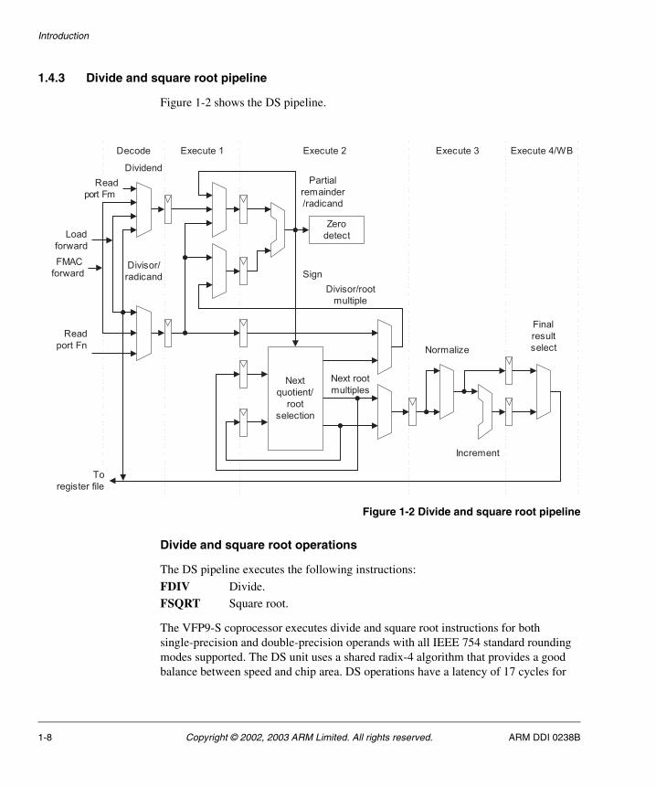
Figure 1-2 shows the DS pipeline.
Figure 1-2 Divide and square root pipeline
Divide and square root operations
The DS pipeline executes the following instructions:
FDIV Divide.
FSQRT Square root.
The VFP9-S coprocessor executes divide and square root instructions for both single-precision and double-precision operands with all IEEE 754 standard rounding modes supported. The DS unit uses a shared radix-4 algorithm that provides a good balance between speed and chip area. DS operations have a latency of 17 cycles for
Read
port Fn
Next root
multiples
Increment
Divisor/root
multiple
Final
result
select
Read
port Fm
Load
forward
FMAC
forward
Zero
detect
Divisor/
radicand
Dividend
Next
quotient/
root
selection
Normalize
Sign
Partial
remainder
/radicand
Execute 2 Execute 3Execute 1Decode Execute 4/WB
To
register file
1-8 Copyright © 2002, 2003 ARM Limited. All rights reserved. ARM DDI 0238B

Introduction
single-precision operations and 31 cycles for double-precision operations. The throughput is 14 cycles for single-precision operations and 28 cycles for double-precision operations.
1.4.4 Load and store pipeline
The LS pipeline handles all of the instructions that transfer data to and from the ARM processor, including loads (LDC and LDM), stores (STC and STM), moves to coprocessor register (MCR and MRCC), and moves from coprocessor register (MRC and MRRC). It remains synchronized with the ARM LS pipeline for the duration of the instruction.
Data written to the ARM processor is read from the VFP9-S register file in the VFP9-S Decode stage and transferred to the ARM processor in the same cycle. The data is latched on the ARM Execute/Memory cycle boundary. The transfer is made on a dedicated 32-bit store data bus between all coprocessors and the ARM processor.
Load data is written to the VFP9-S coprocessor on a dedicated 32-bit load data bus between the ARM processor and all coprocessors. Data is received by the VFP9-S coprocessor on the VFP9-S Memory/Writeback boundary. Data is written to the register file in the VFP9-S Writeback stage, and available for forwarding to CDP operations in the same cycle. Figure 1-3 on page 1-10 shows the LS pipeline.
ARM DDI 0238B Copyright © 2002, 2003 ARM Limited. All rights reserved. 1-9

Introduction
Figure 1-3 Load and store pipeline
Load and store instructions
The LS pipeline executes the following instructions:
FLD Load a single-precision, double-precision, or 32-bit integer value from memory to the VFP9-S register file.
FLDM Load up to 32 single-precision or integer values or 16 double-precision values from memory to the VFP9-S register file.
FST Store a single-precision, double-precision, or 32-bit integer value from the VFP9-S register file to memory.
FSTM Store up to 32 single-precision or integer values or 16 double-precision values from the VFP9-S register file to memory.
FMSR Move a single-precision or integer value from an ARM register to a VFP9-S single-precision register.
FMRS Move a single-precision or integer value from a VFP9-S single-precision register to an ARM register.
ExecuteDecodeFetch
CPINSTR
(instruction
bus)
Fd
Fm
Fn
Store
Load
Read
port Fd
Read
port Fn
Store data
bus
Register
file: read
and
format
muxes
Read
port Fm
FMAC writeback
Memory Writeback
Register
file: write
and
format
muxes
DS forward
Load forward
Load data
bus
FMAC forward
DS writeback
Register
address
generation
1-10 Copyright © 2002, 2003 ARM Limited. All rights reserved. ARM DDI 0238B

Introduction
FMDHR Move an ARM register value to the upper half of a VFP9-S double-precision register.
FMDLR Move an ARM register value to the lower half of a VFP9-S double-precision register.
FMRDH Move the upper half of a double-precision value from a VFP9-S double-precision register to an ARM register.
FMRDL Move the lower half of a double-precision value from a VFP9-S double-precision register to an ARM register.
FMDRR Move two ARM register values to a VFP9-S double-precision register.
FMRRD Move a double-precision VFP9-S register value to two ARM registers.
FMSRR Move two ARM register values to two consecutively-numbered VFP9-S single-precision registers.
FMRRS Move two consecutively-numbered VFP9-S single-precision register values to two ARM registers.
FMXR Move an ARM register value to a VFP9-S control register.
FMRX Move a VFP9-S control register value to an ARM register.
ARM DDI 0238B Copyright © 2002, 2003 ARM Limited. All rights reserved. 1-11

Introduction
1.5 Modes of operation
The VFP9-S coprocessor provides full IEEE 754 standard compatibility through a combination of hardware and software. There are rare cases that require significant additional compute time to resolve correctly according to the requirements of the IEEE 754 standard. For instance, the VFP9-S coprocessor does not process subnormal input values directly. To provide correct handling of subnormal inputs according to the IEEE 754 standard, a trap is made to support code to process the operation. Using the support code for processing this operation can require hundreds of cycles. In some applications this is unavoidable, because compliance with the IEEE 754 standard is essential to proper operation of the program. In many other applications, especially in the embedded market, strict compliance to the IEEE 754 standard is unnecessary, while determinable runtime, low interrupt latency, and low power are of more importance. The following sections describe the two VFP9-S coprocessor modes of operation:
• Full-compliance mode
• Flush-to-Zero mode on page 1-13
• Default NaN mode on page 1-13
• RunFast Mode on page 1-13.
1.5.1 Full-compliance mode
When the VFP9-S coprocessor is in Full-compliance mode, all operations that cannot be processed according to the IEEE 754 standard use support code for assistance. The operations requiring support code are:
• Any CDP operation involving a subnormal input when not in Flush-to-Zero mode. Enable Flush-to-Zero mode by setting the FZ bit, FPSCR[24].
• Any CDP operation involving a NaN input when not in Default NaN mode. Enable Default NaN mode by setting the DN bit, FPSCR[25].
• Any CDP operation that has the potential of generating an underflow condition when not in Flush-to-Zero mode.
• Any CDP operation when Inexact exceptions are enabled. Enable Inexact exceptions by setting the IXE bit, FPSCR[12].
• Any CDP operation that can cause an overflow while Overflow exceptions are enabled. Enable Overflow exceptions by setting the OFE bit, FPSCR[10].
• Any CDP operation that involves an invalid combination as the result of a product overflow when Invalid Operation exceptions are enabled. Enable Invalid Operation exceptions by setting the IOE bit, FPSCR[8].
1-12 Copyright © 2002, 2003 ARM Limited. All rights reserved. ARM DDI 0238B

Introduction
• A float-to-integer conversion that has the potential to create an integer that cannot be represented in the destination integer format when Invalid Operation exceptions are enabled.
The support code:
• determines the nature of the exception
• determines if processing is required to perform the computation
• calls a user trap handler
• transfers control to the user trap handler if the enable bit for the detected exception is set
• writes the result to the destination register, updates the FPSCR register, and returns to the user code if the exception enable bit is not set.
Arithmetic exceptions on page 5-23 describes the conditions under which the VFP9-S coprocessor traps to support code.
1.5.2 Flush-to-Zero mode
Setting the FZ bit, FPSCR[24], enables Flush-to-Zero mode and increases performance on very small inputs and results. In Flush-to-Zero mode, the VFP9-S coprocessor treats all subnormal input operands of arithmetic CDP operations as positive zeros in the operation. Exceptions that result from a zero operand are signaled appropriately. FABS, FCMP, and FNEG are not considered arithmetic CDP operations, and are not affected by Flush-to-Zero mode. A result that is tiny, as described in the IEEE 754 standard, for the destination precision is smaller in magnitude than the minimum normal value before rounding and is replaced with a positive zero. The IDC flag, FPSCR[7], indicates when an input flush occurs. The UFC flag, FPSCR[3], indicates when a result flush occurs.
1.5.3 Default NaN mode
Setting the DN bit, FPSCR[25] enables Default NaN mode. In Default NaN mode, the result of any operation that involves an input NaN or generated a NaN result returns the default NaN. Propagation of the fraction bits is maintained only by FABS, FNEG, and FCPY operations, all other CDP operations ignore any information in the fraction bits of an input NaN. See NaN handling on page 3-5 for a description of default NaNs.
1.5.4 RunFast Mode
RunFast mode is the combination of the following conditions:
• the VFP9-S coprocessor is in Flush-to-Zero mode
• the VFP9-S coprocessor is in Default NaN mode
• all exception enable bits are cleared.
ARM DDI 0238B Copyright © 2002, 2003 ARM Limited. All rights reserved. 1-13
Introduction
In RunFast mode the VFP9-S coprocessor:
• processes subnormal input operands as positive zeros
• processes results that are tiny before rounding, that is, between the positive and negative minimum normal values for the destination precision, as positive zeros
• processes input NaNs as default NaNs
• returns the default result specified by the IEEE 754 standard for overflow, division-by-zero, invalid, or inexact operations fully in hardware and without additional latency
• processes all operations in hardware without trapping to support code.
RunFast mode enables the programmer to write code for the VFP9-S coprocessor that runs in a determinable time without support code assistance, regardless of the characteristics of the input data. In RunFast mode, no user exception traps are available. However, the exception flags in the FPSCR register are compliant with the IEEE 754 standard for Inexact, Overflow, Invalid Operation, and Division-by-Zero exceptions. The underflow flag is modified for Flush-to-Zero mode. Each of these flags is set by an exceptional condition and can by cleared only by a write to the FPSCR register.
1-14 Copyright © 2002, 2003 ARM Limited. All rights reserved. ARM DDI 0238B
Introduction
1.6 Short vector instructions
The VFPv2 architecture supports execution of short vector instructions of up to eight operations on single-precision data and up to four operations on double-precision data. Short vectors are most useful in graphics and signal-processing applications. They reduce code size, increase speed of execution by supporting parallel operations and multiple transfers, and simplify algorithms with high data throughput.
Short vector operations issue the individual operations specified in the instruction in a serial fashion. To eliminate data hazards, short vector operations begin execution only after all source registers are available, and all destination registers are not targets of other operations.
See Chapter 4 Instruction Execution for more information on execution of short vector instructions.
ARM DDI 0238B Copyright © 2002, 2003 ARM Limited. All rights reserved. 1-15
Introduction
1.7 Using CPBURST
When FLDM or FSTM instructions access noncachable data, or when the ARM processor does not have a cache, controlling the CPBURST[3:0] signals can optimize FLDM and FSTM instructions. These signals specify the number of words in a transfer. See the Coprocessor Interface section of the Technical Reference Manual for the ARM9E processor that you are using.
If a load or store multiple requires transferring more than 16 words, the VFP9-S coprocessor drives CPBURST[3:0] to 0000, selecting one-word transfers.
If CPBURST[3:0] = 0000, selecting one-word transfers, then the processor handles each iteration of a load multiple as a single load instruction, greatly inhibiting the performance of the load multiple. Instead of doing a load or store multiple for more than 16 words, split the load or store operation into separate instructions of 16 or fewer words each.
1-16 Copyright © 2002, 2003 ARM Limited. All rights reserved. ARM DDI 0238B

Introduction
1.8 Parallel execution of instructions
The VFP9-S coprocessor can execute several floating-point operations in parallel. While a short vector instruction executes for a number of VFP9-S cycles, it appears to the ARM processor as a single-cycle instruction and is retired in the ARM processor before it completes execution in the VFP9-S coprocessor.
The three pipelines operate independently of one another once initial processing is completed. This makes it possible to issue a short vector operation and a load or store multiple operation in the next cycle, and have both executing at the same time, provided no data hazards exist between the two instructions. Algorithms that can load data while executing instructions can hide much of the data-transfer time in arithmetic operations, significantly improving performance.
Operations in the LS and FMAC pipelines can execute in parallel with scalar DS pipeline operations as long as there are no data hazards between the operations. The DS block has a dedicated write port to the register file, and no special care is required when executing operations in parallel with divide or square root instructions. In short vector DS instructions, the FMAC pipeline is unavailable until the final iteration of the short vector DS operation completes the initial execute cycle. This is described further in Parallel execution on page 4-23.
ARM DDI 0238B Copyright © 2002, 2003 ARM Limited. All rights reserved. 1-17

Introduction
1.9 VFP9-S treatment of branch instructions
The VFP9-S coprocessor does not directly provide branch instructions. Instead, the result of a floating-point compare instruction can be stored in the ARM condition code flags using the FMSTAT instruction. This enables the ARM branch instructions and conditional execution capabilities to be used for executing conditional floating-point code. See section C5 of the ARM Architecture Reference Manual for information on the use of ARM conditional execution to test IEEE 754 standard predicates.
In some cases, full IEEE 754 standard comparisons are not required. Simple comparisons of single-precision data, such as comparisons to zero or to a constant, can be done using an FMRS transfer and the ARM CMP and CMN instructions. This method is faster in many cases than using an FCMP instruction followed by an FMSTAT instruction. For more information, see Compliance with the IEEE 754 standard on page 3-3.
1-18 Copyright © 2002, 2003 ARM Limited. All rights reserved. ARM DDI 0238B

Introduction
1.10 Writing optimal VFP9-S code
The following guidelines provide significant performance increases for VFP9-S code:
• Unless there is a read-after-write hazard, program most scalar operations to immediately follow each other. After a scalar double-precision multiply, multiply-accumulate, or short vector instruction of length greater than one, program either a single ARM instruction or a VFP9-S load or store instruction instead of a VFP9-S FMAC instruction.
• Avoid short vector divides and square roots. The VFP9-S FMAC and DS pipelines are unavailable until the final iteration of the short vector DS operation issues from the Execute 1 stage. If the short vector DS operation can be separated, other VFP9-S instructions can be issued in the cycles immediately following the divide or square root. See An example of parallel execution on page 4-24.
• The best performance for data-intensive applications requires double-buffering looped short vector instructions. The register banks can be divided in half to provide two independent working areas. To take advantage of the simultaneous execution of data transfer and arithmetic instructions, follow the arithmetic instructions on one-half of the bank with loads or stores to the other bank.
• The first VFP9-S instruction following a branch mispredict is serialized and waits for all prior VFP9-S instructions to complete. Avoid placing long load, store, divide, or square root instructions before branches that might not be predicted correctly.
• Moves to and from control registers are serializing. Avoid placing these in loops or time-critical code.
• To prevent read-after-read hazards in Full-compliance mode, avoid reading source operands in the next cycle. See Short vector CDP/store RAR hazard example on page 4-18.
• Avoid using FCMPZ/FCMPEZ if fully compliant IEEE 754 standard comparisons are not required. The use of an FMRS instruction with an ARM CMP or CMN can be faster for simple comparisons. See Comparisons on page 3-6.
ARM DDI 0238B Copyright © 2002, 2003 ARM Limited. All rights reserved. 1-19

Introduction
1.11 Clocking
The VFP9-S coprocessor is a fully static design, with a single clock input, CLK, that can be stopped indefinitely without loss of state. CLK has the same timing requirements as the ARM CLK and is in phase with it. To preserve signal integrity and timing on the coprocessor interface, you must implement the VFP9-S CLK without excessive skew between it and the ARM CLK. For more information on the coprocessor interface, refer to the Technical Refererence Manual for the ARM processor that you are using.
Clock generation within the VFP9-S coprocessor is tightly integrated with the test functionality. See Clock gating on page 6-2 for more information on the impact of test logic on clocking.
1-20 Copyright © 2002, 2003 ARM Limited. All rights reserved. ARM DDI 0238B

Introduction
1.12 Testing
The VFP9-S coprocessor is a full-scan design, with full boundary scan capability for independent testing. See Chapter 6 Design for Test for more information on testing.
ARM DDI 0238B Copyright © 2002, 2003 ARM Limited. All rights reserved. 1-21

Introduction
1.13 Silicon revision information
There is no functional difference between the VFP9-S r0p2 coprocessor and the VFP9-S r0p1 coprocessor.
1-22 Copyright © 2002, 2003 ARM Limited. All rights reserved. ARM DDI 0238B
Chapter 2 Register File
This chapter describes implementation-specific features of the VFP9-S coprocessor that are useful to programmers. It contains the following sections:
• About the register file on page 2-2
• Register file internal formats on page 2-3
• Decoding the register file on page 2-5
• Loading operands from ARM registers on page 2-6
• Maintaining consistency in register precision on page 2-8
• Data transfer between memory and VFP9-S registers on page 2-9
• Access to register banks in CDP operations on page 2-11.
ARM DDI 0238B Copyright © 2002, 2003 ARM Limited. All rights reserved. 2-1

Register File
2.1 About the register file
The VFP9-S register file contains thirty-two 32-bit registers organized in four banks. Each register can store either a single-precision floating-point number or an integer.
Any consecutive pair of registers, [Reven+1]:[Reven], can store a double-precision floating-point number. Because a load or store operation does not modify the data, the VFP9-S registers can also be used as secondary data storage by another application that does not use floating-point values.
For short vector instructions, register addressing is circular within each bank. Load and store operations do not circulate, allowing for multiple banks, up to the entire register file, to be loaded or stored in a single instruction. Short vector operations obey certain rules specifying under what conditions the registers in the argument list specify circular buffers or scalar registers. The LEN and STRIDE fields in the FPSCR register specify the number of operations performed by short vector instructions and the increment scheme within the circular register banks. Further information and examples are in the ARM Architecture Reference Manual, Section C5. The banked approach to the register file supports the use of circular buffers by short vector instructions for applications requiring high data throughput, such as filtering and graphics transforms.
2-2 Copyright © 2002, 2003 ARM Limited. All rights reserved. ARM DDI 0238B

Register File
2.2 Register file internal formats
The VFPv2 architecture provides the option of an internal data format that is different from some or all of the external formats. In this implementation of the VFP9-S coprocessor, data in the register file has the same format as data in memory. Load or store operations for single-precision, double-precision, or integer data do not modify the format. It is the responsibility of the programmer to be aware of the data type in each register. Hardware does not perform any checking of the agreement between the data type in the source registers and the data type expected by the instruction. Hardware always interprets the data according to the precision contained in the instruction. When saving context and restoring VFP9-S data registers, use FLDMX/FSTMX instructions for compatibility with future implementations.
Accessing a register that has not been initialized or loaded with valid data is Unpredictable. A way to detect access to an uninitialized register is to load all registers with Signaling NaNs (SNaNs) in the precision of the initial access of the register and enable the Invalid Operation exception.
2.2.1 Integer data format
The VFP9-S coprocessor supports signed and unsigned 32-bit integers. Signed integers are treated as two’s complement values. Figure 2-1 shows the integer format for signed and unsigned integers.
Figure 2-1 Integer format
No modification to the data is implicit in a load, store, or transfer operation on integer data. The format of integer data within the register file is identical to the format in memory or in an ARM general-purpose register.
2.2.2 Single-precision data format
Figure 2-2 shows the single-precision bit fields.
Figure 2-2 Single-precision data format
31 0
Integer
31
FractionS Exponent
22 030 23
ARM DDI 0238B Copyright © 2002, 2003 ARM Limited. All rights reserved. 2-3
Register File
The single-precision data format contains:
• the sign bit, bit [31]
• the exponent, bits [30:23]
• the fraction, bits [22:0].
The IEEE 754 standard defines the single-precision data format of the VFP9-S coprocessor. Refer to the IEEE 754 standard for details about:
• the exponent bias
• special formats
• numerical ranges.
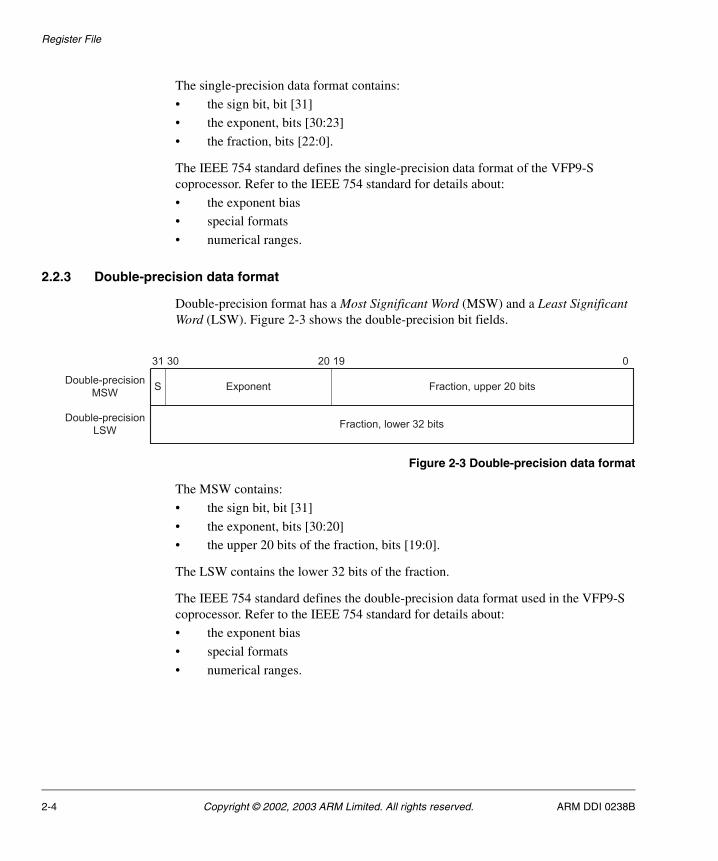
2.2.3 Double-precision data format
Double-precision format has a Most Significant Word (MSW) and a Least Significant Word (LSW). Figure 2-3 shows the double-precision bit fields.
Figure 2-3 Double-precision data format
The MSW contains:
• the sign bit, bit [31]
• the exponent, bits [30:20]
• the upper 20 bits of the fraction, bits [19:0].
The LSW contains the lower 32 bits of the fraction.
The IEEE 754 standard defines the double-precision data format used in the VFP9-S coprocessor. Refer to the IEEE 754 standard for details about:
• the exponent bias
• special formats
• numerical ranges.
31
Exponent Fraction, upper 20 bitsS
30 20 19 0
Fraction, lower 32 bits
Double-precision
MSW
Double-precision
LSW
2-4 Copyright © 2002, 2003 ARM Limited. All rights reserved. ARM DDI 0238B

Register File
2.3 Decoding the register file
Each register file access uses five bits of the register number in the instruction word. For instructions with double-precision operands or destinations, the M, N, and D bit corresponding to a double-precision access must be cleared. For single-precision and integer accesses, the most significant four bits are in the Fm, Fn, or Fd field, and the least significant bit is the M, N, or D bit for each instruction format. Figure 2-4 shows the register file. See the ARM Architecture Reference Manual for instruction formats and the positions of these bits.
Figure 2-4 Register file access
31 0
S1
S3
S7
S5
S9
S11
S13
S15
S17
S19
S21
S23
S25
S27
S29
S31
031
63 0
D0
D1
D2
D3
D4
D5
D6
D7
D8
D9
D10
D11
D12
D13
D14
D15
S2
S4
S6
S8
S10
S12
S14
S16
S18
S20
S22
S24
S26
S28
S30
S0
ARM DDI 0238B Copyright © 2002, 2003 ARM Limited. All rights reserved. 2-5
Register File
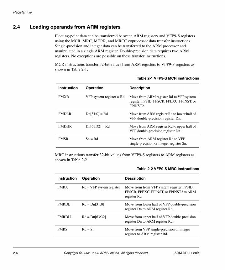
2.4 Loading operands from ARM registers
Floating-point data can be transferred between ARM registers and VFP9-S registers using the MCR, MRC, MCRR, and MRCC coprocessor data transfer instructions. Single-precision and integer data can be transferred to the ARM processor and manipulated in a single ARM register. Double-precision data requires two ARM registers. No exceptions are possible on these transfer instructions.
MCR instructions transfer 32-bit values from ARM registers to VFP9-S registers as shown in Table 2-1.
MRC instructions transfer 32-bit values from VFP9-S registers to ARM registers as shown in Table 2-2.
Table 2-1 VFP9-S MCR instructions
Instruction Operation Description
FMXR VFP system register = Rd Move from ARM register Rd to VFP system register FPSID, FPSCR, FPEXC, FPINST, or FPINST2.
FMDLR Dn[31:0] = Rd Move from ARM register Rd to lower half of VFP double-precision register Dn.
FMDHR Dn[63:32] = Rd Move from ARM register Rd to upper half of VFP double-precision register Dn.
FMSR Sn = Rd Move from ARM register Rd to VFP single-precision or integer register Sn.
Table 2-2 VFP9-S MRC instructions
Instruction Operation Description
FMRX Rd = VFP system register Move from from VFP system register FPSID, FPSCR, FPEXC, FPINST, or FPINST2 to ARM register Rd.
FMRDL Rd = Dn[31:0] Move from lower half of VFP double-precision register Dn to ARM register Rd.
FMRDH Rd = Dn[63:32] Move from upper half of VFP double-precision register Dn to ARM register Rd.
FMRS Rd = Sn Move from VFP single-precision or integer register to ARM register Rd.
2-6 Copyright © 2002, 2003 ARM Limited. All rights reserved. ARM DDI 0238B

Register File
MCRR instructions transfer 64-bit quantities from ARM registers to VFP9-S registers, as Table 2-3 shows.
Table 2-4 describes MRRC transfers.
Table 2-3 VFP9-S MCRR instructions
Instruction Operation Description
FMDRR Dm[lower half] = RdDm[upper half] = Rn
Move from ARM registers Rd and Rn to lower and upper halves of VFP double-precision register Dm.
FMSRR Sm = RdS(m + 1) = Rn
Move from ARM registers Rd and Rn to consecutive VFP single-precision registers Sm and S(m + 1).
Table 2-4 VFP9-S MRRC instructions
Instruction Operation Description
FMRRD Rd = Dm[lower half]Rn = Dm[upper half]
Move from lower and upper halves of VFP double-precision register Dm to ARM registers Rd and Rn.
FMRRS Rd = SmRn = S(m + 1)
Move from single-precision VFP registers Sm and S(m + 1) to ARM registers Rd and Rn.
ARM DDI 0238B Copyright © 2002, 2003 ARM Limited. All rights reserved. 2-7

Register File
2.5 Maintaining consistency in register precision
The VFP9-S register file stores single-precision, double-precision, and integer data in the same registers. For example, D6 occupies the same registers as S12 and S13. The usable format of the register or registers depends on the last load or arithmetic instruction that wrote to the register or registers.
The hardware does not check the register format to see if it is consistent with the precision of the current operation. Inconsistent use of the registers is possible but Unpredictable. The data is interpreted by the hardware in the format required by the instruction regardless of the latest store or write operation to the register. It is the task of the compiler or programmer to maintain consistency in register usage.
2-8 Copyright © 2002, 2003 ARM Limited. All rights reserved. ARM DDI 0238B

Register File
2.6 Data transfer between memory and VFP9-S registers
The B bit in the CP15 control register determines whether access to stored memory is little-endian or big-endian. The ARM processor supports both little-endian and big-endian access formats in memory.
The ARM processor stores 32-bit words in memory with the Least Significant Byte (LSB) in the lowest byte of the memory address regardless of the endianness selected. For a store of a single-precision value, the LSB is located at the target address with the lower two bits of the address cleared. The Most Significant Byte (MSB) is at the target address with the lower two bits set. To load the single-precision data to an ARM register or to a VFP9-S register you must clear the lower two bits of the target address.
Table 2-5 shows how single-precision data is stored in memory and the address access to each byte in both little-endian and big-endian formats. In this example, the target address is 0x40000000.
Table 2-5 Single-precision data memory images and byte addresses
Single-precisiondata bytes
Address inmemory
Little-endianbyte address
Big-endianbyte address
MSB, bits [31:24] 0x40000003 0x40000003 0x40000000
Bits [23:16] 0x40000002 0x40000002 0x40000001
Bits [15:8] 0x40000001 0x40000001 0x40000002
LSB, bits [7:0] 0x40000000 0x40000000 0x40000003
ARM DDI 0238B Copyright © 2002, 2003 ARM Limited. All rights reserved. 2-9
Register File
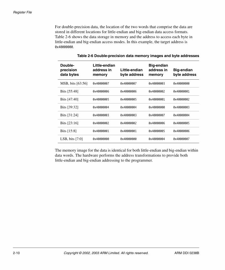
For double-precision data, the location of the two words that comprise the data are stored in different locations for little-endian and big-endian data access formats. Table 2-6 shows the data storage in memory and the address to access each byte in little-endian and big-endian access modes. In this example, the target address is 0x40000000.
The memory image for the data is identical for both little-endian and big-endian within data words. The hardware performs the address transformations to provide both little-endian and big-endian addressing to the programmer.
Table 2-6 Double-precision data memory images and byte addresses
Double-precisiondata bytes
Little-endianaddress inmemory
Little-endianbyte address
Big-endianaddress inmemory
Big-endianbyte address
MSB, bits [63:56] 0x40000007 0x40000007 0x40000003 0x40000000
Bits [55:48] 0x40000006 0x40000006 0x40000002 0x40000001
Bits [47:40] 0x40000005 0x40000005 0x40000001 0x40000002
Bits [39:32] 0x40000004 0x40000004 0x40000000 0x40000003
Bits [31:24] 0x40000003 0x40000003 0x40000007 0x40000004
Bits [23:16] 0x40000002 0x40000002 0x40000006 0x40000005
Bits [15:8] 0x40000001 0x40000001 0x40000005 0x40000006
LSB, bits [7:0] 0x40000000 0x40000000 0x40000004 0x40000007
2-10 Copyright © 2002, 2003 ARM Limited. All rights reserved. ARM DDI 0238B

Register File
2.7 Access to register banks in CDP operations
The register file is especially suited for short vector operations. You can use four banks of registers in a circular fashion to facilitate signal processing and matrix operations. For details of this refer to the ARM Architecture Reference Manual.
2.7.1 About register banks
As Figure 2-5 shows, the register file is divided into four banks with eight registers in each bank for single-precision instructions and four registers per bank for double-precision instructions. CDP instructions access the banks in a circular manner. Load and store multiple instructions do not access the registers in a circular manner but treat the register file as a linearly ordered structure.
See ARM Architecture Reference Manual, Part C for more information on VFP addressing modes.
Figure 2-5 Register banks
A short vector CDP operation that has a source or destination vector crossing a bank boundary wraps around and accesses the first register in the bank.
Example 2-1 on page 2-12 shows the iterations of the following short vector add instruction with a length of six iterations (LEN = 101).
FADDS S11, S22, S31
Example 2-1 on page 2-12 shows the short vector FADDS operations.
S24
S25
S26
S27
S28
S29
S30
S31
Bank 3
D12
D13
D14
D15
S17
S18
S19
S20
S21
S22
S16
Bank 2
D8
D9
D10
D11S23
S8
S9
S10
S11
S12
S13
S14
S15
Bank 1
D4
D5
D6
D7
S3
S2
S4
S5
S6
S7
S0
S1
Bank 0
D0
D1
D2
D3
ARM DDI 0238B Copyright © 2002, 2003 ARM Limited. All rights reserved. 2-11

Register File
Example 2-1 Register bank wrapping
FADDS S11, S22, S31 ; 1st iteration FADDS S12, S23, S24 ; 2nd iteration. The 2nd source vector wraps around
; and accesses the 1st register in the 4th bankFADDS S13, S16, S25 ; 3rd iteration. The 1st source vector wraps around
; and accesses the 1st register in the 3rd bankFADDS S14, S17, S26 ; 4th iterationFADDS S15, S18, S27 ; 5th iterationFADDS S8, S19, S28 ; 6th and last iteration. The destination vector
; wraps around and writes to the 1st register in the; 2nd bank
2.7.2 Operations using register banks
The register file organization supports four types of operations described in the following sections:
• Scalar-only instructions
• Short vector-only instructions on page 2-13
• Short vector instructions with scalar source on page 2-13
• Scalar instructions in short vector mode on page 2-14.
See Floating-point status and control register, FPSCR on page 3-17 for details of the LEN and STRIDE fields and the FPSCR register.
Scalar-only instructions
An instruction is a scalar-only operation if the operands are treated as scalars and the result is a scalar.
Clearing the LEN field in the FPSCR register selects a vector length of one iteration. For example, if LEN is cleared, then the following operation writes the sum of the single-precision values in S21 and S22 to S12:
FADDS S12, S21, S22
Some instructions can operate only on scalar data regardless of the value in the LEN field or destination register bank number. These instructions are:
• compare FCMPS/D, FCMPZS/D, FCMPES/D, and FCMPEZS/D
• integer conversion FTOUIS/D, FTOUIZS/D, FTOSIS/D, FTOSIZS/D, FUITOS/D, and FSITOS/D
• precision conversion FCVTDS and FCVTSD.
2-12 Copyright © 2002, 2003 ARM Limited. All rights reserved. ARM DDI 0238B
Register File
Short vector-only instructions
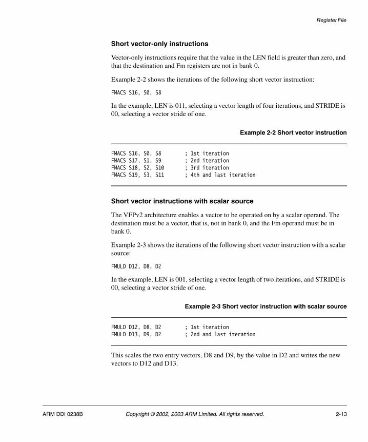
Vector-only instructions require that the value in the LEN field is greater than zero, and that the destination and Fm registers are not in bank 0.
Example 2-2 shows the iterations of the following short vector instruction:
FMACS S16, S0, S8
In the example, LEN is 011, selecting a vector length of four iterations, and STRIDE is 00, selecting a vector stride of one.
Example 2-2 Short vector instruction
FMACS S16, S0, S8 ; 1st iterationFMACS S17, S1, S9 ; 2nd iterationFMACS S18, S2, S10 ; 3rd iterationFMACS S19, S3, S11 ; 4th and last iteration
Short vector instructions with scalar source
The VFPv2 architecture enables a vector to be operated on by a scalar operand. The destination must be a vector, that is, not in bank 0, and the Fm operand must be in bank 0.
Example 2-3 shows the iterations of the following short vector instruction with a scalar source:
FMULD D12, D8, D2
In the example, LEN is 001, selecting a vector length of two iterations, and STRIDE is 00, selecting a vector stride of one.
Example 2-3 Short vector instruction with scalar source
FMULD D12, D8, D2 ; 1st iterationFMULD D13, D9, D2 ; 2nd and last iteration
This scales the two entry vectors, D8 and D9, by the value in D2 and writes the new vectors to D12 and D13.
ARM DDI 0238B Copyright © 2002, 2003 ARM Limited. All rights reserved. 2-13
Register File
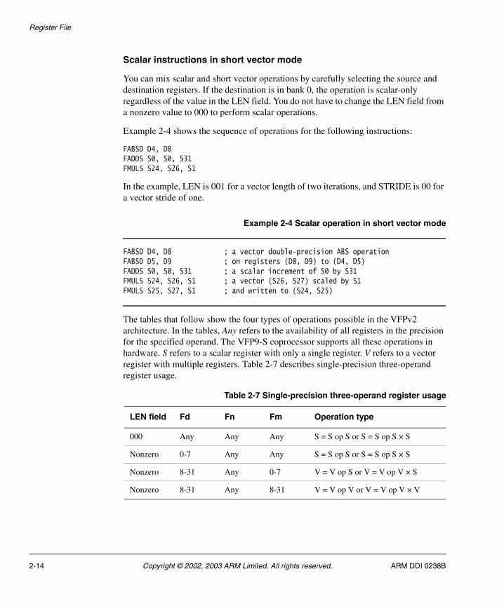
Scalar instructions in short vector mode
You can mix scalar and short vector operations by carefully selecting the source and destination registers. If the destination is in bank 0, the operation is scalar-only regardless of the value in the LEN field. You do not have to change the LEN field from a nonzero value to 000 to perform scalar operations.
Example 2-4 shows the sequence of operations for the following instructions:
FABSD D4, D8FADDS S0, S0, S31FMULS S24, S26, S1
In the example, LEN is 001 for a vector length of two iterations, and STRIDE is 00 for a vector stride of one.
Example 2-4 Scalar operation in short vector mode
FABSD D4, D8 ; a vector double-precision ABS operationFABSD D5, D9 ; on registers (D8, D9) to (D4, D5)FADDS S0, S0, S31 ; a scalar increment of S0 by S31FMULS S24, S26, S1 ; a vector (S26, S27) scaled by S1FMULS S25, S27, S1 ; and written to (S24, S25)
The tables that follow show the four types of operations possible in the VFPv2 architecture. In the tables, Any refers to the availability of all registers in the precision for the specified operand. The VFP9-S coprocessor supports all these operations in hardware. S refers to a scalar register with only a single register. V refers to a vector register with multiple registers. Table 2-7 describes single-precision three-operand register usage.
Table 2-7 Single-precision three-operand register usage
LEN field Fd Fn Fm Operation type
000 Any Any Any S = S op S or S = S op S × S
Nonzero 0-7 Any Any S = S op S or S = S op S × S
Nonzero 8-31 Any 0-7 V = V op S or V = V op V × S
Nonzero 8-31 Any 8-31 V = V op V or V = V op V × V
2-14 Copyright © 2002, 2003 ARM Limited. All rights reserved. ARM DDI 0238B

Register File
Table 2-8 describes single-precision two-operand register usage.
Table 2-9 describes double-precision three-operand register usage.
Table 2-10 describes double-precision two-operand register usage.
Table 2-8 Single-precision two-operand register usage
LEN field Fd Fm Operation type
000 Any Any S = op S
Nonzero 0-7 Any S = op S
Nonzero 8-31 0-7 V= op S
Nonzero 8-31 8-31 V= op V
Table 2-9 Double-precision three-operand register usage
LEN field Fd Fn Fm Operation type
000 Any Any Any S = S op S or S = S op S × S
Nonzero 0-3 Any Any S = S op S or S = S op S × S
Nonzero 4-15 Any 0-3 V = V op S or V = V op V × S
Nonzero 4-15 Any 4-15 V = V op V or V = V op V × V
Table 2-10 Double-precision two-operand register usage
LEN field Fd Fm Operation type
000 Any Any S = op S
Nonzero 0-3 Any S = op S
Nonzero 4-15 0-3 V= op S
Nonzero 4-15 4-15 V= op V
ARM DDI 0238B Copyright © 2002, 2003 ARM Limited. All rights reserved. 2-15

Register File
2-16 Copyright © 2002, 2003 ARM Limited. All rights reserved. ARM DDI 0238B
Chapter 3 Programmer’s Model
This chapter describes implementation-specific features of the VFP9-S coprocessor that are useful to programmers. It contains the following sections:
• About the programmer’s model on page 3-2
• Compliance with the IEEE 754 standard on page 3-3
• ARMv5TE coprocessor extensions on page 3-9
• VFP9-S system control and status registers on page 3-15.
ARM DDI 0238B Copyright © 2002, 2003 ARM Limited. All rights reserved. 3-1

Programmer’s Model
3.1 About the programmer’s model
This section introduces the VFP9-S implementation of the VFPv2 floating-point architecture. Issue E of the ARM Architecture Reference Manual describes the VFPv1 architecture.
The VFP9-S coprocessor implements all the instructions and modes of the VFPv2 architecture. The VFPv2 architecture adds the following features and enhancements to the VFPv1 architecture:
• The ARM v5TE instruction set, which includes MRRC and MCRR 64-bit ARM-to-coprocessor transfer instructions. These instructions allow the transfer of a double-precision register, or two consecutively numbered single-precision registers, to or from a pair of ARM registers. See Loading operands from ARM registers on page 2-6 for syntax and usage of VFP MRRC and MCRR instructions.
• Default NaN mode. In Default NaN mode, any operation involving one or more NaN operands produces the default NaN as a result, rather than returning the NaN or one of the NaNs involved in the operation. This mode is compatible with the IEEE 754 standard but not with current handling of NaNs by industry.
• Addition of the input subnormal flag, IDC (FPSCR[7]). IDC is set whenever the VFP9-S coprocessor is in Flush-to-Zero mode and a subnormal input operand is replaced by a positive zero. It remains set until cleared by writing to the FPSCR register. A new Input Subnormal exception enable bit, IDE (FPSCR[15]), is also added. When IDE is set, the VFP9-S coprocessor traps to the UNDEFINED trap handler for an instruction that asserts IDC.
• New functionality of the underflow flag, UFC (FPSCR[3]), in Flush-to-Zero mode. In Flush-to-Zero mode, UFC is set whenever a result is below the threshold for normal numbers before rounding, and the result is flushed to zero. UFC remains set until cleared by writing to the FPSCR register. The Underflow exception enable bit, UFE (FPSCR[11]), does not cause a trap to the UNDEFINED trap handler on an assertion of UFC.
• New functionality of the inexact flag, IXC (FPSCR[4]), in Flush-to-Zero mode. In VFPv1, IXC is set when an input or result is flushed to zero. In VFPv2, the IDC and UFC flags provide this information. See Inexact exception on page 5-21 for more information.
• Addition of RunFast mode. See RunFast Mode on page 1-13 for details of RunFast mode operation.
3-2 Copyright © 2002, 2003 ARM Limited. All rights reserved. ARM DDI 0238B

Programmer’s Model
3.2 Compliance with the IEEE 754 standard
This section introduces issues related to compliance with the IEEE 754 standard:
• why compliance is important
• hardware and software components
• software-based components and their availability.
3.2.1 An IEEE 754 standard-compliant implementation
The VFP9-S hardware and support code together provide IEEE 754 standard-compliant implementations of all the VFPv2 floating-point instructions. Unless an enabled floating-point exception occurs, it appears to the program that the floating-point instruction was executed by the hardware. If an exceptional condition occurs that requires software support during instruction execution, the instruction takes significantly more cycles than normal to produce the result. This is a common practice in the industry, and the incidence of such instructions is typically very low.
3.2.2 Complete implementation of the IEEE 754 standard
The following operations from the IEEE 754 standard are not supplied by the VFP9-S instruction set:
• remainder
• round floating-point number to integer-valued floating-point number
• binary-to-decimal conversions
• decimal-to-binary conversions
• direct comparison of single-precision and double-precision values.
For complete implementation of the IEEE 754 standard, the VFP9-S coprocessor and support code must be augmented with library functions that implement the above operations. See AFS Firmware Suite Reference Guide for details of support code and the available library functions.
3.2.3 IEEE 754 standard implementation choices
Some of the implementation choices allowed by the IEEE 754 standard and used in the VFPv2 architecture are described in Part C of the ARM Architecture Reference Manual.
Further implementation choices are made within the VFP9-S coprocessor about which cases are handled by the VFP9-S hardware and which cases bounce to the support code.
ARM DDI 0238B Copyright © 2002, 2003 ARM Limited. All rights reserved. 3-3
Programmer’s Model
To execute frequently encountered operations as fast as possible and minimize silicon area, handling of rarely occurring values and some exceptions is relegated to the support code. The VFP9-S coprocessor supports two modes for handling rarely occurring values:
• Full-compliance mode with support code assistance is fully compliant with the IEEE 754 standard. Full-compliance mode requires the floating-point support code to handle certain operands and exceptional conditions not supported in the hardware. Although the support code gives full compliance with the IEEE 754 standard, it can increase the runtime of an application and the size of kernel code.
• RunFast mode is almost fully compliant with the IEEE 754 standard in hardware alone. Default handling for subnormal inputs, underflows, and NaN inputs is not fully compliant with the IEEE 754 standard. No user trap handlers are allowed in this mode.
When Flush-to-Zero and Default NaN modes are enabled, and all exceptions are disabled, the VFP9-S coprocessor operates in RunFast mode. While the potential loss of accuracy for very small values is present, RunFast mode removes a significant number of performance-limiting stall conditions. By not requiring the floating-point support code, RunFast mode enables increased performance of typical and optimized code and a reduction in the size of kernel code. See Hazards on page 4-7 for more information on performance improvements in RunFast mode.
Supported formats
The supported formats are:
• Single-precision and double-precision. No extended format is supported.
• Integer formats:
— unsigned 32-bit integers
— two’s complement signed 32-bit integers.
3-4 Copyright © 2002, 2003 ARM Limited. All rights reserved. ARM DDI 0238B

Programmer’s Model
NaN handling
Any single-precision or double-precision values with the maximum exponent field value and a nonzero fraction field are valid NaNs. A most significant fraction bit of zero indicates an SNaN. A one indicates a Quiet NaN (QNaN). Two NaN values are treated as different NaNs if they differ in any bit. Table 3-1 shows the default NaN values in both single and double precision.
Any SNaN passed as input to an operation causes an Invalid Operation exception, which is passed to a user trap handler, if present. If a user trap handler is not present, then a default QNaN is created. The rules for cases involving multiple NaN operands are in the ARM Architecture Reference Manual.
Processing of input NaNs for ARM floating-point coprocessors and libraries is defined as follows:
• In Full-compliance mode, NaNs are handled according to the ARM Architecture Reference Manual. The hardware does not process the NaNs directly for arithmetic CDP instructions, but traps to the support code for all NaN processing. For data transfer operations, NaNs are transferred without raising the Invalid Operation exception or trapping to support code. For the nonarithmetic CDP instructions, FABS, FNEG, and FCPY, NaNs are copied, with a change of sign if specified in the instructions, without causing the Invalid Operation exception or trapping to support code.
• In RunFast mode, NaNs are handled completely within the hardware without support code assistance. SNaNs in an arithmetic CDP operation set the IOC flag, FPSCR[0]. NaN handling by data transfer and nonarithmetic CDP instructions is the same as in Full-compliance mode. Arithmetic CDP instructions involving NaN operands return the default NaN regardless of the fractions of any NaN operands. Although this is a departure from the behavior of most hardware floating-point units in the industry, it is compliant with the IEEE 754 standard.
Table 3-1 Default NaN values
Single-precision Double-precision
Sign 0 0
Exponent 0xFF 0x7FF
Fraction bit [22] = 1bits [21:0] are all zeros
bit [51] = 1bits [50:0] are all zeros
ARM DDI 0238B Copyright © 2002, 2003 ARM Limited. All rights reserved. 3-5

Programmer’s Model
Comparisons
Comparison results modify condition code flags in the FPSCR register. The FMSTAT instruction transfers the current condition code flags in the FPSCR register to the ARM CPSR register. Refer to the ARM Architecture Reference Manual for mapping of IEEE 754 standard predicates to ARM conditions. The condition code flags used are chosen so that subsequent conditional execution of ARM instructions can test the predicates defined in the IEEE 754 standard.
The VFP9-S handles most comparisons of numeric values in hardware, generating the appropriate condition code depending on whether the result is less than, equal, or greater than. When the VFP9-S is not in Flush-to-Zero mode, comparisons involving subnormal operands bounce to support code. When the VFP9-S is not in Default NaN mode, comparisons involving NaNs bounce to support code.
The VFP9-S coprocessor supports:
• compare operations FCMPS, FCMPZS, FCMPD, and FCMPZD
A compare instruction involving an SNaN produces an unordered result and generates an Invalid Operation exception. If the IOE bit, FPSCR[8], is set, the user trap handler is called. A QNaN compares as unordered but does not generate an Invalid Operation exception.
• compare with exception operations FCMPES, FCMPEZS, FCMPED, and FCMPEDZ
A compare with exception operation involving either an SNaN or a QNaN produces an unordered result and generates an Invalid Operation exception.
Some simple comparisons on single-precision data can be computed directly by the ARM processor. If only equality or comparison to zero is needed, and NaNs are not an issue, performing the comparison in ARM registers using CMP or CMN instructions can be faster.
If branching on the state of the Z flag is needed, the following instructions can be used for positive values:
FMRS Rx,SnCMP Rx,#0BEQ label
If the input values can include negative numbers, including negative zero, the following code can be used:
FMRS Rx, SnCMP Rx, #0x80000000CMPNE Rx, #0BEQ label
Using a temporary register is even faster:
3-6 Copyright © 2002, 2003 ARM Limited. All rights reserved. ARM DDI 0238B
Programmer’s Model
FMRS Rx,SnMOVS Rt,Rx,LSL #1BEQ label
Comparisons with particular values are also possible. For example, to check if a positive value is greater or equal to +1.0, use:
FMRS Rx,SnCMP Rx,#0x3F800000BGE label
When comparisons are required for double-precision values, or when IEEE 754 standard comparisons are required, it is safer to use the FCMP and FCMPE instructions with FMSTAT.
Underflow
In the generation of Underflow exceptions, the after rounding form of tininess and the subnormalization loss form of loss of accuracy as described in the IEEE 754 standard are used.
In Flush-to-Zero mode, results that are tiny before rounding, as described in the IEEE 754 standard, are flushed to a positive zero, and the UFC flag, FPSCR[3], is set. Support code is not involved. See Part C of the ARM Architecture Reference Manual for information on Flush-to-Zero mode.
When the VFP9-S coprocessor is not in Flush-to-Zero mode, any operation with a risk of producing a tiny result, as described in the IEEE 754 standard, bounces to support code. If the operation does not produce a tiny result, it returns the computed result, and the UFC flag, FPSCR[3], is not set. The IXC flag, FPSCR[4], is set if the operation is inexact. If the operation produces a tiny result, the result is a subnormal or zero value, and the UFC flag, FPSCR[3], is set. See Underflow exception on page 5-19 for more information on underflow handling.
Exceptions
Exceptions are taken in the VFP9-S coprocessor in an imprecise manner. When exception processing begins, the states of the ARM processor and the VFP9-S coprocessor might not be the same as when the exception occurred. Exceptional instructions cause the VFP9-S coprocessor to enter the exceptional state, and the next VFP9-S instruction triggers exception processing. After the issue of the exceptional instruction and before exception processing begins, non-VFP9-S instructions and some VFP9-S instructions can be executed and retired. Any source registers involved in the exceptional instruction are preserved, and the destination register is not overwritten on entry to the support code. If the detected exception enable bit is not set, the support code returns to the program flow at the point of the trigger instruction after processing the
ARM DDI 0238B Copyright © 2002, 2003 ARM Limited. All rights reserved. 3-7

Programmer’s Model
exception. If the detected exception enable bit is set, and a user trap handler is installed, the support code passes control to the user trap handler. If the exception is overflow or underflow, the intermediate result specified by the IEEE 754 standard is made available to the user trap handler.
Note
The precise set of facilities available are system-dependent.
3-8 Copyright © 2002, 2003 ARM Limited. All rights reserved. ARM DDI 0238B
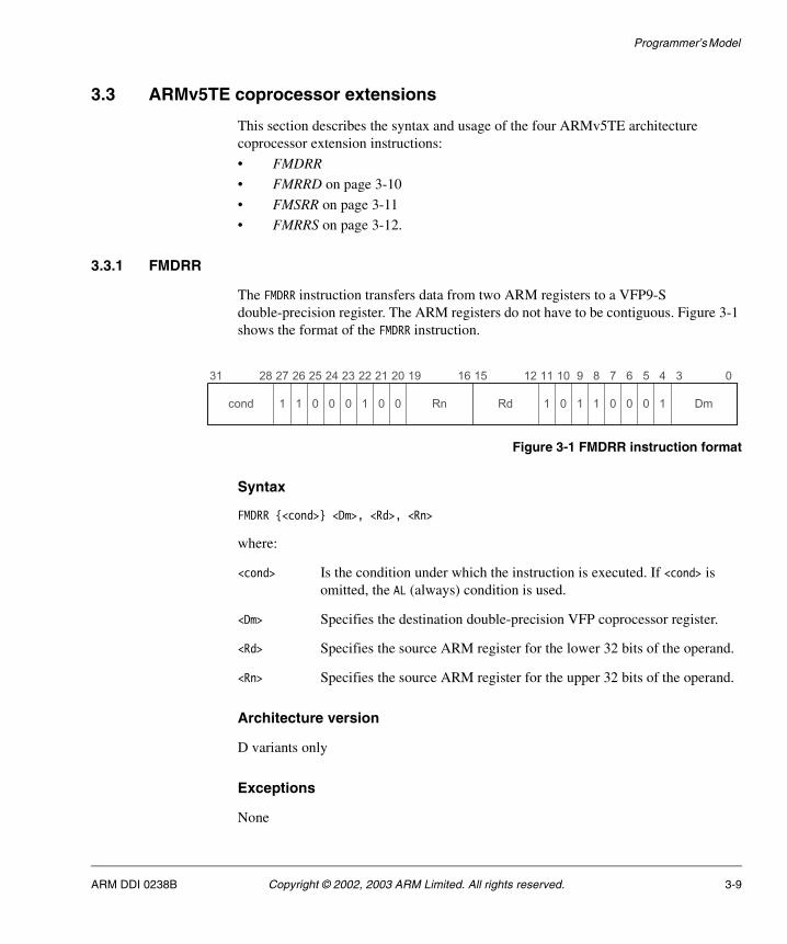
Programmer’s Model
3.3 ARMv5TE coprocessor extensions
This section describes the syntax and usage of the four ARMv5TE architecture coprocessor extension instructions:
• FMDRR
• FMRRD on page 3-10
• FMSRR on page 3-11
• FMRRS on page 3-12.
3.3.1 FMDRR
The FMDRR instruction transfers data from two ARM registers to a VFP9-S double-precision register. The ARM registers do not have to be contiguous. Figure 3-1 shows the format of the FMDRR instruction.
Figure 3-1 FMDRR instruction format
Syntax
FMDRR {<cond>} <Dm>, <Rd>, <Rn>
where:
<cond> Is the condition under which the instruction is executed. If <cond> is omitted, the AL (always) condition is used.
<Dm> Specifies the destination double-precision VFP coprocessor register.
<Rd> Specifies the source ARM register for the lower 32 bits of the operand.
<Rn> Specifies the source ARM register for the upper 32 bits of the operand.
Architecture version
D variants only
Exceptions
None
27 26 25 24 23 22 21 20 11 10 9 8 7 6 5 4
1 Dm1 0 0 011 0Rd0 Rn0 0 1 01 1 0cond
31 28 19 16 15 12 3 0
ARM DDI 0238B Copyright © 2002, 2003 ARM Limited. All rights reserved. 3-9

Programmer’s Model
Operation
if ConditionPassed(cond) thenDm[upper half] = RnDm[lower half] = Rd
Notes
Conversions In the programmer’s model, FMDRR does not perform any conversion of the value transferred. Arithmetic instructions using either Rd or Rn treat the value as an integer, whereas most VFP instructions treat the Dm value as a double-precision floating-point number.
3.3.2 FMRRD
The FMRRD instruction transfers data in a VFP9-S double-precision register to two ARM registers. The ARM registers do not have to be contiguous. Figure 3-2 shows the format of the FMRRD instruction.
Figure 3-2 FMRRD instruction format
Syntax
FMRRD {<cond>} <Rd>, <Rn>, <Dm>
where:
<cond> Is the condition under which the instruction is executed. If <cond> is omitted, the AL (always) condition is used.
<Rd> Specifies the destination ARM register for the lower 32 bits of the operand.
<Rn> Specifies the destination ARM register for the upper 32 bits of the operand.
<Dm> Specifies the source double-precision VFP coprocessor register.
27 26 25 24 23 22 21 20 11 10 9 8 7 6 5 4
1 Dm1 0 0 011 0Rd1 Rn0 0 1 01 1 0cond
31 28 19 16 15 12 3 0
3-10 Copyright © 2002, 2003 ARM Limited. All rights reserved. ARM DDI 0238B
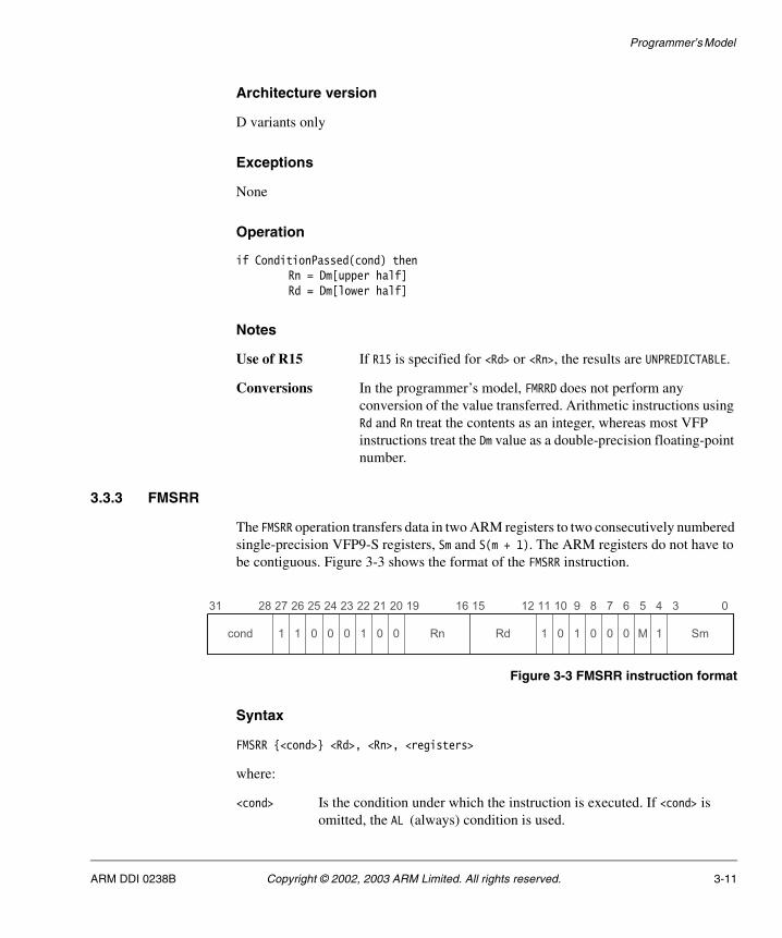
Programmer’s Model
Architecture version
D variants only
Exceptions
None
Operation
if ConditionPassed(cond) thenRn = Dm[upper half]Rd = Dm[lower half]
Notes
Use of R15 If R15 is specified for <Rd> or <Rn>, the results are UNPREDICTABLE.
Conversions In the programmer’s model, FMRRD does not perform any conversion of the value transferred. Arithmetic instructions using Rd and Rn treat the contents as an integer, whereas most VFP instructions treat the Dm value as a double-precision floating-point number.
3.3.3 FMSRR
The FMSRR operation transfers data in two ARM registers to two consecutively numbered single-precision VFP9-S registers, Sm and S(m + 1). The ARM registers do not have to be contiguous. Figure 3-3 shows the format of the FMSRR instruction.
Figure 3-3 FMSRR instruction format
Syntax
FMSRR {<cond>} <Rd>, <Rn>, <registers>
where:
<cond> Is the condition under which the instruction is executed. If <cond> is omitted, the AL (always) condition is used.
27 26 25 24 23 22 21 20 11 10 9 8 7 6 5 4
1 Sm0 0 0 M11 0Rd0 Rn0 0 1 01 1 0cond
31 28 19 16 15 12 3 0
ARM DDI 0238B Copyright © 2002, 2003 ARM Limited. All rights reserved. 3-11

Programmer’s Model
<Rd> Specifies the source ARM register for the Sm VFP9-S single-precision register.
<Rn> Specifies the source ARM register for the S(m + 1) VFP9-S single-precision register.
<registers> Specifies the pair of consecutively numbered single-precision destination VFP9-S registers, separated by a comma and surrounded by brackets. If m is the number of the first register in the list, the list is encoded in the instruction by setting Sm to the top four bits of m and M to the bottom bit of m. For example, if <registers> is {S1, S2}, the Sm field of the instruction is 0000 and the M bit is 1.
Architecture version
All
Exceptions
None
Operation
If ConditionPassed(cond) thenSm = RdS(m + 1) = Rn
Notes
Conversions In the programmer’s model, FMSRR does not perform any conversion of the value transferred. Arithmetic instructions using Rd and Rn treat the contents as an integer, whereas most VFP instructions treat the Sm and S(m + 1) values as single-precision floating-point numbers.
Invalid register lists
If Sm is 1111 and M is 1 (an encoding of S31) the instruction is UNPREDICTABLE.
3.3.4 FMRRS
The FMRRS operation transfers data in two consecutively numbered single-precision VFP9-S registers to two ARM registers. The ARM registers do not have to be contiguous. Figure 3-4 on page 3-13 shows the format of the FMRRS instruction.
3-12 Copyright © 2002, 2003 ARM Limited. All rights reserved. ARM DDI 0238B

Programmer’s Model
Figure 3-4 FMRRS instruction format
Syntax
FMRRS {<cond>} <Rd>, <Rn>, <registers>
where:
<cond> Is the condition under which the instruction is executed. If <cond> is omitted, the AL (always) condition is used.
<Rd> Specifies the destination ARM register for the Sm VFP coprocessor single-precision value.
<Rn> Specifies the destination ARM register for the S(m + 1) VFP coprocessor single-precision value.
<registers> Specifies the pair of consecutively numbered single-precision source VFP coprocessor registers, separated by a comma and surrounded by brackets. If m is the number of the first register in the list, the list is encoded in the instruction by setting Sm to the top four bits of m and M to the bottom bit of m. For example, if <registers> is {S16, S17}, the Sm field of the instruction is 1000 and the M bit is 0.
Architecture version
All
Exceptions
None
Operation
If ConditionPassed(cond) thenRd = SmRn = S(m + 1)
27 26 25 24 23 22 21 20 11 10 9 8 7 6 5 4
1 Sm0 0 0 M11 0Rd1 Rn0 0 1 01 1 0cond
31 28 19 16 15 12 3 0
ARM DDI 0238B Copyright © 2002, 2003 ARM Limited. All rights reserved. 3-13

Programmer’s Model
Notes
Conversions In the programmer’s model, FMRRS does not perform any conversion of the value transferred. Arithmetic instructions using Rd and Rn treat the contents as an integer, whereas most VFP9-S instructions treat the Sm and S(m + 1) values as single-precision floating-point numbers.
Invalid register lists
If Sm is 1111 and M is 1 (an encoding of S31) the instruction is UNPREDICTABLE
Use of R15 If R15 is specified for Rd or Rn, the results are UNPREDICTABLE.
3-14 Copyright © 2002, 2003 ARM Limited. All rights reserved. ARM DDI 0238B
Programmer’s Model
3.4 VFP9-S system control and status registers
The VFP9-S coprocessor provides sufficient information for processing all exception conditions encountered by the hardware. In an exceptional situation, the hardware provides
• the exceptional instruction
• the instruction that was issued to the VFP9-S coprocessor before the exception was detected
• exception status information
— type of exception
— number of remaining short vector iterations after an exceptional iteration.
Five VFP9-S registers support exceptional conditions:
• Floating-point system ID register (FPSID)
• Floating-point status and control register (FPSID)
• Floating-point exception register (FPEXC).
• Floating-point instruction register (FPINST)
• Floating-point instruction register 2 (FPINST2)
These registers are designed to be used with the support code software available from ARM Limited. As a result, this document does not fully specify exception handling in all cases.
In addition, the source data registers for an exceptional instruction are available to the support code. However, some or all of the other data registers in the ARM9E processor and the VFP9-S coprocessor might be modified and not in the state they were in at the time the exceptional instruction was issued.
ARM DDI 0238B Copyright © 2002, 2003 ARM Limited. All rights reserved. 3-15

Programmer’s Model
Access to the FPEXC, FPINST, and FPINST2 registers is possible only in a privileged mode, and does not trigger exceptions. Use the FMRX instruction to store these registers and the FMXR instruction to load them. Table 3-2 describes access to these registers.
The following sections describe the VFP9-S control and status registers:
• Floating-point system ID register, FPSID
• Floating-point status and control register, FPSCR on page 3-17
• Floating-point exception register, FPEXC on page 3-20
• Instruction registers, FPINST and FPINST2 on page 3-23.
3.4.1 Floating-point system ID register, FPSID
The FPSID register is a read-only register that contains the value 0x410101A0, identifying the VFP9-S coprocessor. Figure 3-5 shows the bit fields of the FPSID register.
Figure 3-5 Floating-point system ID register
Table 3-2 Access to control registers
RegisterFMXR/FMRX <reg>field encoding
Exception processingtrigger? Legal modes
FPSID 0000 No Any
FPSCR 0001 No Any
FPEXC 1000 No Privileged
FPINST 1001 No Privileged
FPINST2 1010 No Privileged
Architecture
23 20
RevisionVariantPart numberSNGSWImplementer Format
3 07 415 819 1622 2131 24
3-16 Copyright © 2002, 2003 ARM Limited. All rights reserved. ARM DDI 0238B
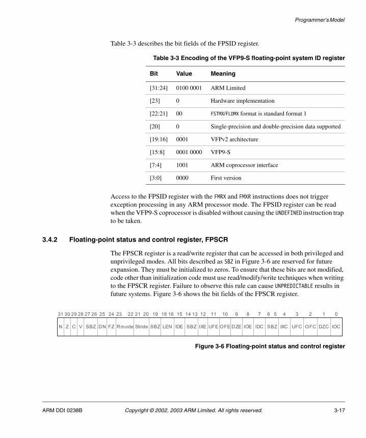
Programmer’s Model
Table 3-3 describes the bit fields of the FPSID register.
Access to the FPSID register with the FMRX and FMXR instructions does not trigger exception processing in any ARM processor mode. The FPSID register can be read when the VFP9-S coprocessor is disabled without causing the UNDEFINED instruction trap to be taken.
3.4.2 Floating-point status and control register, FPSCR
The FPSCR register is a read/write register that can be accessed in both privileged and unprivileged modes. All bits described as SBZ in Figure 3-6 are reserved for future expansion. They must be initialized to zeros. To ensure that these bits are not modified, code other than initialization code must use read/modify/write techniques when writing to the FPSCR register. Failure to observe this rule can cause UNPREDICTABLE results in future systems. Figure 3-6 shows the bit fields of the FPSCR register.
Figure 3-6 Floating-point status and control register
Table 3-3 Encoding of the VFP9-S floating-point system ID register
Bit Value Meaning
[31:24] 0100 0001 ARM Limited
[23] 0 Hardware implementation
[22:21] 00 FSTMX/FLDMX format is standard format 1
[20] 0 Single-precision and double-precision data supported
[19:16] 0001 VFPv2 architecture
[15:8] 0001 0000 VFP9-S
[7:4] 1001 ARM coprocessor interface
[3:0] 0000 First version
31 30 29 28 25 24 23 22 21 20 19 15 12 11 10 9 8 7 4 3 2 1 0
IXCIDC SBZDZE IOEUFE OFESBZ IXEIDELENRmode Stride SBZSBZ DN FZN Z C V UFC OFC DZC IOC
27 26 18 16 14 13 6 5
ARM DDI 0238B Copyright © 2002, 2003 ARM Limited. All rights reserved. 3-17

Programmer’s Model
Table 3-4 describes the bit fields of the FPSCR register.
Table 3-4 Encoding of floating-point status and control register
Bit Name Meaning
[31] N Set if comparison produces a less than result.
[30] Z Set if comparison produces an equal result.
[29] C Set if comparison produces an equal, greater than, or unordered result.
[28] V Set if comparison produces an unordered result.
[27:26] SBZ Should be zero.
[25] DN Default NaN mode enable bit.1 = Default NaN mode enabled0 = Default NaN mode disabled.
[24] FZ Flush-to-Zero mode enable bit.1 = Flush-to-Zero mode enabled0 = Flush-to-Zero mode disabled.
[23:22] Rmode Rounding mode control field.00 = round-to-nearest01 = round-toward-plus-infinity10 = round-toward-minus-infinity11 = round-toward-zero.
[21:20] Stride See Vector length and stride control on page 3-19.
[19] SBZ Should be zero.
[18:16] LEN See Vector length and stride control on page 3-19.
[15] IDE Input Subnormal (denormalized) exception enable bit.
[14:13] SBZ Should be zero.
[12] IXE Inexact exception enable bit.
[11] UFE Underflow exception enable bit.
[10] OFE Overflow exception enable bit.
[9] DZE Division-by-Zero exception enable bit.
[8] IOE Invalid Operation exception enable bit.
[7] IDC Input Subnormal (denormalized) cumulative flag.
3-18 Copyright © 2002, 2003 ARM Limited. All rights reserved. ARM DDI 0238B
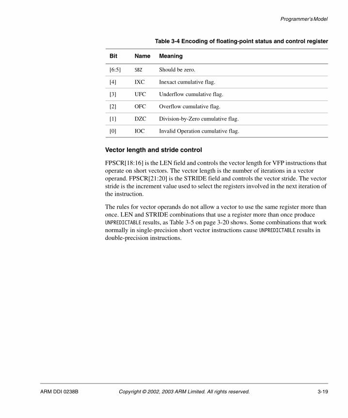
Programmer’s Model
Vector length and stride control
FPSCR[18:16] is the LEN field and controls the vector length for VFP instructions that operate on short vectors. The vector length is the number of iterations in a vector operand. FPSCR[21:20] is the STRIDE field and controls the vector stride. The vector stride is the increment value used to select the registers involved in the next iteration of the instruction.
The rules for vector operands do not allow a vector to use the same register more than once. LEN and STRIDE combinations that use a register more than once produce UNPREDICTABLE results, as Table 3-5 on page 3-20 shows. Some combinations that work normally in single-precision short vector instructions cause UNPREDICTABLE results in double-precision instructions.
[6:5] SBZ Should be zero.
[4] IXC Inexact cumulative flag.
[3] UFC Underflow cumulative flag.
[2] OFC Overflow cumulative flag.
[1] DZC Division-by-Zero cumulative flag.
[0] IOC Invalid Operation cumulative flag.
Table 3-4 Encoding of floating-point status and control register
Bit Name Meaning
ARM DDI 0238B Copyright © 2002, 2003 ARM Limited. All rights reserved. 3-19
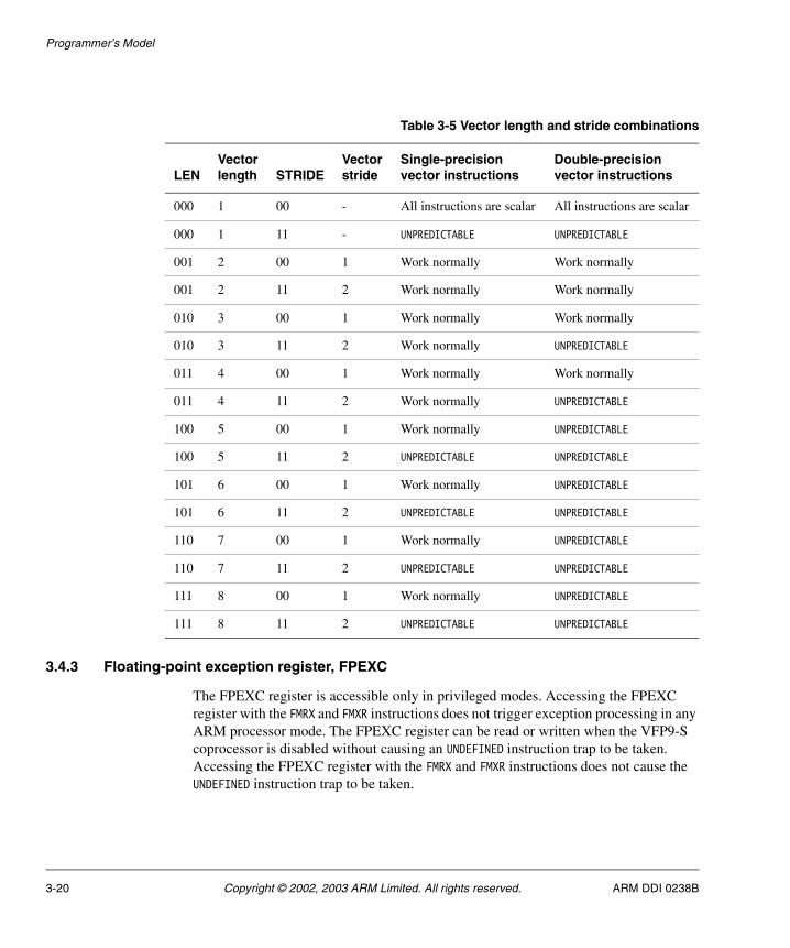
Programmer’s Model
3.4.3 Floating-point exception register, FPEXC
The FPEXC register is accessible only in privileged modes. Accessing the FPEXC register with the FMRX and FMXR instructions does not trigger exception processing in any ARM processor mode. The FPEXC register can be read or written when the VFP9-S coprocessor is disabled without causing an UNDEFINED instruction trap to be taken. Accessing the FPEXC register with the FMRX and FMXR instructions does not cause the UNDEFINED instruction trap to be taken.
Table 3-5 Vector length and stride combinations
LENVectorlength STRIDE
Vectorstride
Single-precisionvector instructions
Double-precisionvector instructions
000 1 00 - All instructions are scalar All instructions are scalar
000 1 11 - UNPREDICTABLE UNPREDICTABLE
001 2 00 1 Work normally Work normally
001 2 11 2 Work normally Work normally
010 3 00 1 Work normally Work normally
010 3 11 2 Work normally UNPREDICTABLE
011 4 00 1 Work normally Work normally
011 4 11 2 Work normally UNPREDICTABLE
100 5 00 1 Work normally UNPREDICTABLE
100 5 11 2 UNPREDICTABLE UNPREDICTABLE
101 6 00 1 Work normally UNPREDICTABLE
101 6 11 2 UNPREDICTABLE UNPREDICTABLE
110 7 00 1 Work normally UNPREDICTABLE
110 7 11 2 UNPREDICTABLE UNPREDICTABLE
111 8 00 1 Work normally UNPREDICTABLE
111 8 11 2 UNPREDICTABLE UNPREDICTABLE
3-20 Copyright © 2002, 2003 ARM Limited. All rights reserved. ARM DDI 0238B

Programmer’s Model
You must save and restore the FPEXC register whenever changing the context. If the EX flag, FPEXC[31], is set, then the VFP9-S coprocessor is in the exceptional state, and you must also save and restore the FPINST and FPINST2 registers. You can write the context switch code to determine from the EX flag which registers to save and restore, or to simply save all three.
The EN bit, FPEXC[30], is the VFP enable bit. Clearing EN disables the VFP9-S coprocessor.
In a bounce situation, the exceptional condition is recorded in the FPEXC register. The FPEXC register information assists the support code in processing the exceptional condition or reporting the condition to a system trap handler or a user trap handler.
The exception flags in the FPEXC register detect exceptional conditions pessimistically. This means that the flags are set when the hardware detects only the potential for an exception in the Execute 1 stage. Not until the last stage or after the instruction has been performed by the support code can it be known if a true exception exists.
The INV flag, FPEXC[7], signals Input exceptions. An Input exception is a condition in which the hardware cannot process one or more input operands according to the architectural specifications. This includes subnormal inputs when the VFP9-S coprocessor is not in Flush-to-Zero mode and NaNs when the VFP9-S coprocessor is not in Default NaN mode.
The UFC flag, FPEXC[3], is set whenever an operation has the potential to generate a result that is below the minimum threshold for the destination precision.
The OFC flag, FPEXC[2], is set whenever an operation has the potential to generate a result that, after rounding, exceeds the largest representable number in the destination format.
The IOC flag, FPEXC[2], is set whenever an operation has the potential to generate a result that cannot be represented or is not defined.
Note To prevent an infinite loop of exceptions, the support code must clear the EX flag, FPEXC[31], immediately on entry to the exception code. All exception flags must be cleared before returning from exception code to user code.
Figure 3-7 on page 3-22 shows the bit fields of the FPEXC register.
ARM DDI 0238B Copyright © 2002, 2003 ARM Limited. All rights reserved. 3-21

Programmer’s Model
Figure 3-7 Floating-point exception register
Table 3-6 describes the bit fields of the FPEXC register.
IOC
31 30 29 28 10 8 7 6 4 3 2 1 0
SBZSBZ UFC OFCINVVECITRSBZEX EN SBZ FP2V
27 11
Table 3-6 Encoding of the floating-point exception register
Bit Name Description
[31] EX Exception flag.
When EX is set, the VFP9-S coprocessor is in the exceptional state.
[30] EN Enable VFP bit.
Setting EN enables VFP9-S coprocessor. Reset clears EN.
[29] SBZ Should be zero.
[28] FP2V FPINST2 register instruction valid flag.Set when FPINST2 contains a valid instruction.
[27:11] SBZ Should be zero.
[10:8] VECITR Vector iteration count field.
VECITR contains the number of remaining short vector iterations after a potential exception was detected in one of the iterations.
000 = 1 iteration001 = 2 iterations010 = 3 iterations011 = 4 iterations100 = 5 iterations101 = 6 iterations110 = 7 iterations111 = 0 iterations.
[7] INV Input exception flag
Set if the VFP9-S coprocessor is not in Flush-to-Zero mode and an operand is subnormal or if the VFP9-S coprocessor is not in Default NaN mode and an operand is a NaN.
[6:4] SBZ Should be zero.
[3] UFC Underflow cumulative flag.
Set if the VFP9-S coprocessor is not in Flush-to-Zero mode and a potential underflow condition exists.
3-22 Copyright © 2002, 2003 ARM Limited. All rights reserved. ARM DDI 0238B

Programmer’s Model
3.4.4 Instruction registers, FPINST and FPINST2
The VFP9-S coprocessor has two instruction registers:
• The FPINST register contains the exceptional instruction.
• The FPINST2 register contains the instruction that was issued to the VFP9-S coprocessor before the exception was detected. This instruction was retired in the ARM processor and cannot be reissued. It must be executed by support code.
The instruction in the FPINST register is in the same format as the issued instruction but is modified in several ways. The condition code flags, FPINST[31:28], are forced to 1110, the AL (always) condition. If the instruction is a short vector, the source and destination registers that reference vectors are updated to point to the source and destination registers of the exceptional iteration. See Exception processing for CDP short vector instructions on page 5-8 for more information.
The instruction in the FPINST2 register is in the same format as the issued instruction but is modified by forcing the condition code flags, FPINST2[31:28] to 1110, the AL (always) condition.
[2] OFC Overflow cumulative flag.
Set if the OFE bit, FPSCR[10], is set, the VFP9-S coprocessor is not in RunFast mode, and a potential overflow condition exists.
[1] SBZ Should be zero.
[0] IOC Invalid operation cumulative flag.
Set if the IOE bit, FPSCR[8], is set, the VFP9-S coprocessor is not in RunFast mode, and a potential invalid operation condition exists.
Table 3-6 Encoding of the floating-point exception register (continued)
Bit Name Description
ARM DDI 0238B Copyright © 2002, 2003 ARM Limited. All rights reserved. 3-23

Programmer’s Model
3-24 Copyright © 2002, 2003 ARM Limited. All rights reserved. ARM DDI 0238B

Chapter 4 Instruction Execution
This chapter describes the VFP9-S instruction pipeline and its relationship with the ARM9E instruction pipeline. It contains the following sections:
• About instruction execution on page 4-2
• Serializing instructions on page 4-3
• Interrupting the VFP9-S coprocessor on page 4-4
• Forwarding on page 4-5
• Hazards on page 4-7
• Parallel execution on page 4-23
• Execution timing on page 4-26.
ARM DDI 0238B Copyright © 2002, 2003 ARM Limited. All rights reserved. 4-1

Instruction Execution
4.1 About instruction execution
Because of the nature of the ARM9E coprocessor interface, the VFP9-S coprocessor hardware fetches one instruction every other clock cycle.
The advanced VFP9-S coprocessor features, particularly the short vector instructions and the circular hardware register banks, are further enhanced by a high-performance coprocessor interface that enables execution of several VFP9-S operations in parallel. The ARM9E processor sees the short vector operation as a single-cycle operation. It issues subsequent ARM9E instructions, including VFP9-S load and store instructions, while the VFP9-S short vector instruction is iterating.
One application that benefits significantly from this parallelism is filtering. VFP9-S short vector operations can do multiply-accumulate operations while the previous results are stored to memory, or the next data set is loaded from memory. This results in superscalar performance from a uniscalar processor. See An example of parallel execution on page 4-24 for a more detailed description of the parallel execution capabilities of the VFP9-S coprocessor.
4-2 Copyright © 2002, 2003 ARM Limited. All rights reserved. ARM DDI 0238B

Instruction Execution
4.2 Serializing instructions
Serializing instructions stall the VFP9-S coprocessor in the Fetch stage and the ARM9E processor in the Execute stage until:
• the VFP9-S pipeline is past the point of updating either the condition codes or exception status
• a write to a system register can no longer affect the operation of a current or pending instruction.
Uses of serializing instructions include:
• capturing condition codes and exception status
• delineating a block of instructions for execution with the ability to capture the exception status of that block of instructions
• modifying the mode of operation of subsequent instructions, such as the rounding mode or vector length.
The serializing instructions are FMRX and FMXR, including the FMSTAT instruction. An FMRX or FMSTAT instruction stalls until all prior floating-point operations are completed, and the data to be written to the ARM9E processor is valid. For example, a compare operation updates the FPSCR register condition codes in the Writeback stage of the compare. Reading the FPSCR register stalls until the writeback is complete. Reading the FPEXC register stalls until after all prior CDP instructions complete the Writeback stage. Reading FPINST and FPINST2 stalls until after all prior instructions pass the Execute 1 stage.
An FMXR instruction stalls until all prior floating-point operations are past the point of being affected by the instruction. For example, writing to the FPSCR register stalls until the point when changing the control bits cannot affect any operation currently executing or awaiting execution. Writing to the FPEXC, FPINST, or FPINST2 register stalls until the pipeline is completely clear.
While no instruction can change the contents of the FPSID register, you can access the FPSID register with FMRX or FMXR as a general-purpose serializing operation or to create an exception boundary.
ARM DDI 0238B Copyright © 2002, 2003 ARM Limited. All rights reserved. 4-3

Instruction Execution
4.3 Interrupting the VFP9-S coprocessor
Instructions are issued to the VFP9-S coprocessor directly from the ARM Fetch stage. The VFP9-S coprocessor has no external interface beyond the ARM9E processor and cannot be separately interrupted by external sources. Any interrupt that causes a change of flow in the ARM9E processor is also reflected to the VFP9-S coprocessor. Any VFP instruction that is cancelled in the ARM pipeline is also cancelled in the VFP9-S pipeline.
If the interrupt is the result of a Data Abort condition, the load or store operation that caused the abort is restarted after interrupt processing is complete. Load and store multiple instructions can detect some exception conditions and interrupt the operation after the initial transfer. If the load or store instruction is reissued after interrupt processing, it can restart with the initial transfer. The source data is guaranteed to be unchanged, and no operations that depend on the load or store data can execute until the load or store operation is complete.
When interrupt processing begins, there can be a delay before the VFP9-S coprocessor is available to the interrupt routine. To prevent data hazards in a context switch, any prior short vector instruction that passed the ARM Execute stage must also pass the VFP9-S Execute 1 stage. The maximum delay is equal to the time it takes to process a short vector of eight single-precision divide or square root iterations. Such an operation causes a delay of 114 cycles after the divide or square root enters the VFP9-S Execute 1 stage.
4-4 Copyright © 2002, 2003 ARM Limited. All rights reserved. ARM DDI 0238B

Instruction Execution
4.4 Forwarding
The VFP9-S coprocessor forwards data from load instructions and CDP instructions to CDP instructions. In general, any forwarding operation reduces the stall time of a dependent instruction by one cycle.
In the examples that follow, the stall counts given are based on two data transfer assumptions:
• accesses by load operations result in cache hits and are able to deliver one data word per cycle
• store operations write directly to the write buffer or cache and can transfer one data word per cycle.
When these assumptions are valid, the VFP9-S coprocessor operates at its highest performance. When these assumptions are not valid, load and store operations are affected by the delay required to access data. The examples below illustrate the capabilities of the VFP9-S coprocessor in ideal conditions.
The VFP9-S coprocessor does not forward in the following cases:
• from an instruction that produces integer data
• to a store instruction (FST, FSTM, MRC, or MRRC)
• to an instruction of different precision.
In Example 4-1, the second FADDS instruction depends on the result of the first FADDS instruction. The result of the first FADDS instruction is forwarded, reducing the stall from four cycles to three cycles.
Example 4-1 Data forwarded to dependent instruction
FADDS S1, S2, S3FADDS S8, S9, S1
In Example 4-2, the data is not forwarded from the FTOUIS instruction. The FSTS instruction stalls for three cycles.
Example 4-2 Data not forwarded from integer-producing instruction
FTOUIS S2, S1FSTS S2, [Rx]
ARM DDI 0238B Copyright © 2002, 2003 ARM Limited. All rights reserved. 4-5
Instruction Execution
In Example 4-3, there is no data forwarding of the double-precision FMULD data in D2 to the single-precision FADDS data in S5, even though S5 is the upper half of D2.
Example 4-3 Mixed-precision data not forwarded
FMULD D2, D0, D1FADDS S12, S13, S5
In Example 4-4, the double-precision FSTD stalls for five cycles until the result of the FMULD is written to the register file. No forwarding is done from the FMULD to the store instruction.
Example 4-4 Data not forwarded to store instruction
FMULD D1, D2, D3FSTD D1, [Rx]
4-6 Copyright © 2002, 2003 ARM Limited. All rights reserved. ARM DDI 0238B

Instruction Execution
4.5 Hazards
The VFP9-S coprocessor incorporates full hazard detection with a fully-interlocked pipeline protocol. No compiler scheduling is required to avoid hazard conditions. The scoreboard processes interlocks caused by unavailable source or destination registers or by unavailable data. The scoreboard stalls instructions until all data operands or registers are available when required.
The determination of hazards and interlock conditions is different in Full-compliance mode and RunFast mode. RunFast mode guarantees no bounce conditions and has a less strict hazard detection mechanism, enabling instructions to begin execution earlier than in Full-compliance mode. Full-compliance mode on page 4-8 and RunFast mode on page 4-9 describe these differences.
There are three VFP9-S pipeline hazards:
• A data hazard is created by a combination of instructions that requires operands to be accessed in a certain order.
— A Read-After-Write (RAW) data hazard occurs when the the pipeline creates the potential for an instruction to read an operand before a prior instruction has written to it. It is a hazard to the intended read-after-write operand access.
— A Write-After-Read (WAR) data hazard occurs when the pipeline creates the potential for an instruction to write to a register before a prior instruction has read it. It is a hazard to the intended write-after-read operand access.
— A Write-After-Write (WAW) data hazard occurs when the pipeline creates the potential for an instruction to write to a register before a prior instruction has written to it. It is a hazard to the intended write-after-write operand access.
• A Read-After-Read (RAR) condition is not a hazard in the sense of a RAW, WAR, or WAW hazard. The VFP9-S coprocessor does not distinguish between source and destination registers. A RAR hazard does not cause incorrect data to be read, so it is not a data hazard. However, it is a control hazard because the scoreboard treats a RAR hazard the same as a RAW, WAR, or WAW hazard. See Operation of the scoreboard on page 4-8.
• Resource hazard. See Resource hazards on page 4-19.
ARM DDI 0238B Copyright © 2002, 2003 ARM Limited. All rights reserved. 4-7

Instruction Execution
4.6 Operation of the scoreboard
The scoreboard lock register contains one bit for each register that is not available to an instruction in the next cycle. The scoreboard makes no distinction between source registers and destination registers, so the VFP9-S coprocessor detects RAR hazards as valid hazards (see Hazards on page 4-7).
Source registers locked for a store multiple instruction are cleared in the Execute stage of the instruction. Source registers locked for scalar CDP instructions are cleared in the Execute 1 stage. Source registers for short vector instructions are cleared in the Execute 1 stage of each iteration.
Destination registers are cleared in the cycle before they are written back to the register file or available for forwarding. Destination registers are cleared in the scoreboard lock register in the Execute 3 stage for CDP instructions and in the Memory stage for load and store instructions.
The registers involved in an operation, both as source and destination, are determined in the Decode stage of the VFP9-S pipeline, and a lock mask is generated. Registers involved in each iteration of a short vector operation are included in the lock mask. The determination of the source registers that are included in the lock mask is a function of the mode, RunFast or Full-compliance (see Data hazards in Full-compliance mode on page 4-14 and Data hazards in RunFast mode on page 4-18). The scoreboard lock register is checked and updated in the Decode stage. If a hazard is detected, the lock register is not updated and the instruction stalls in Decode.
Note The register clearing and the lock register checking happen in parallel, with the cleared registers not available to the check operation until the following cycle. The clearing is done in the cycle before the data is available and does not stall an operation unless the data is not available in the next cycle.
4.6.1 Full-compliance mode
When a bounce occurs on any operation, all source registers for that operation, and for any iterations remaining after the bounced iteration, must be unchanged by subsequent instructions. This causes RAW, WAR, and RAR hazards to introduce stalls in the pipeline. The scoreboard does not distinguish between source and destination registers and continues to detect hazards on any involved register until the lock on that register is cleared. If a source register is not also the destination, its lock is cleared in the Execute 1 stage. Destination register locks are cleared in the next-to-last Execute stage, Execute 3.
4-8 Copyright © 2002, 2003 ARM Limited. All rights reserved. ARM DDI 0238B

Instruction Execution
4.6.2 RunFast mode
RunFast mode guarantees that no bouncing is possible, so there is no need to preserve source registers. For all scalar operations and nonmultiple store operations, no source registers are locked. For short vector instructions, the length of the vector determines which source registers are locked. Source registers are locked when the vector length exceeds four single-precision iterations or two double-precision iterations.
Short vector instructions can begin execution only when all registers involved in the operation are free of locks. When a short vector instruction proceeds in the pipeline beyond the Decode stage, all registers involved in the instruction are locked. If the source register is not also the destination register, each iteration clears its source register lock in the Execute 1 stage. The destination register lock is cleared in the next-to-last Execute stage, Execute 3.
4.6.3 Single-precision source register locking
The scoreboard locks source registers in the Decode stage of the instruction and clears source registers in the Execute 1 stage of each iteration. Table 4-1 shows how the scoreboard locks source registers for single-precision instructions in Full-compliance mode and in RunFast mode.
For example, the following single-precision short vector instruction has a vector length of five iterations (LEN = 100):
Table 4-1 Single-precision source register locking
LENVectorlength
Source registers locked in Decode stage
Full-compliance mode RunFast mode
000 1 Iteration 1 registers -
001 2 Iterations 1-2 registers -
010 3 Iterations 1-3 registers -
011 4 Iterations 1-4 registers -
100 5 Iterations 1-5 registers Iteration 5 registers
101 6 Iterations 1-6 registers Iterations 5-6 registers
110 7 Iterations 1-7 registers Iterations 5-7 registers
111 8 Iterations 1-8 registers Iterations 5-8 registers
ARM DDI 0238B Copyright © 2002, 2003 ARM Limited. All rights reserved. 4-9

Instruction Execution
FADDS S8, S16, S24
In Full-compliance mode, the FADDS performs the following operations:
FADDS S8, S16, S24 ; S16 and S24 locked in Decode stageFADDS S9, S17, S25 ; S17 and S25 locked in Decode stageFADDS S10, S18, S26 ; S18 and S26 locked in Decode stageFADDS S11, S19, S27 ; S19 and S27 locked in Decode stageFADDS S12, S20, S28 ; S20 and S28 locked in Decode stage
In RunFast mode, the FADDS performs the following operations:
FADDS S8, S16, S24 ; No registers lockedFADDS S9, S17, S25 ; No registers lockedFADDS S10, S18, S26 ; No registers lockedFADDS S11, S19, S27 ; No registers lockedFADDS S12, S20, S28 ; S20 and S28 locked in Decode stage
4.6.4 Single-precision source register clearing
Table 4-2 shows how the scoreboard clears source registers for single-precision instructions in Full-compliance mode and in RunFast mode.
For example, the following single-precision short vector instruction has a vector length of five iterations (LEN = 100):
Table 4-2 Single-precision source register clearing
Execute 1cycle
Source registers cleared in Execute 1 stage of each iteration
Full-compliance mode RunFast mode
1 Iteration 1 registers Iteration 5 registers
2 Iteration 2 registers Iteration 6 registers
3 Iteration 3 registers Iteration 7 registers
4 Iteration 4 registers Iteration 8 registers
5 Iteration 5 registers -
6 Iteration 6 registers -
7 Iteration 7 registers -
8 Iteration 8 registers -
4-10 Copyright © 2002, 2003 ARM Limited. All rights reserved. ARM DDI 0238B
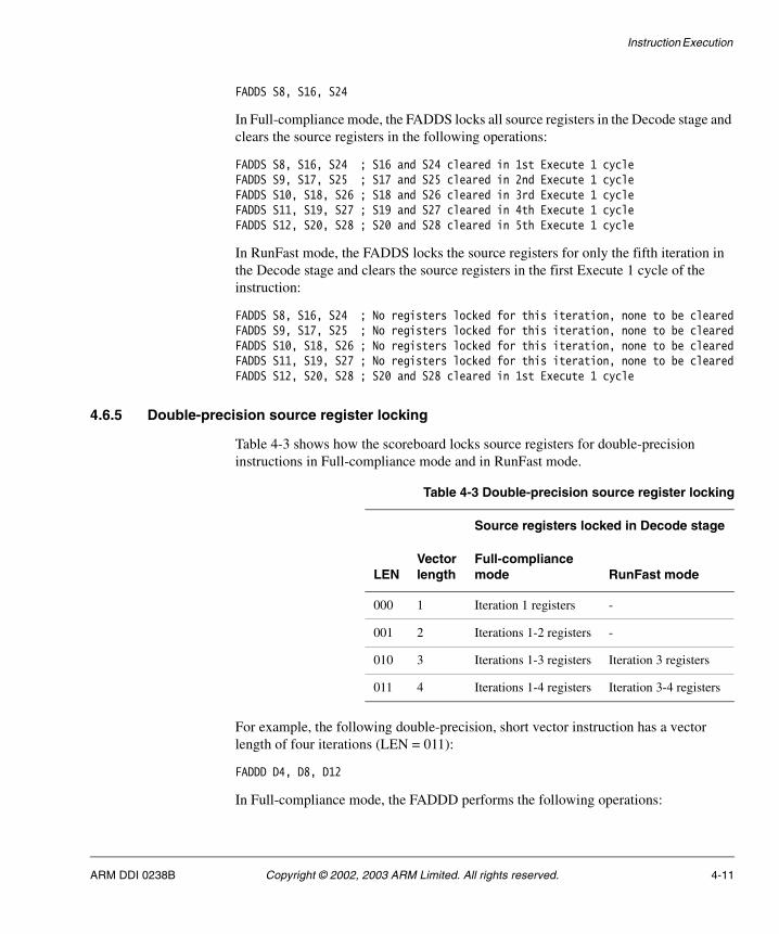
Instruction Execution
FADDS S8, S16, S24
In Full-compliance mode, the FADDS locks all source registers in the Decode stage and clears the source registers in the following operations:
FADDS S8, S16, S24 ; S16 and S24 cleared in 1st Execute 1 cycleFADDS S9, S17, S25 ; S17 and S25 cleared in 2nd Execute 1 cycleFADDS S10, S18, S26 ; S18 and S26 cleared in 3rd Execute 1 cycleFADDS S11, S19, S27 ; S19 and S27 cleared in 4th Execute 1 cycleFADDS S12, S20, S28 ; S20 and S28 cleared in 5th Execute 1 cycle
In RunFast mode, the FADDS locks the source registers for only the fifth iteration in the Decode stage and clears the source registers in the first Execute 1 cycle of the instruction:
FADDS S8, S16, S24 ; No registers locked for this iteration, none to be clearedFADDS S9, S17, S25 ; No registers locked for this iteration, none to be clearedFADDS S10, S18, S26 ; No registers locked for this iteration, none to be clearedFADDS S11, S19, S27 ; No registers locked for this iteration, none to be clearedFADDS S12, S20, S28 ; S20 and S28 cleared in 1st Execute 1 cycle
4.6.5 Double-precision source register locking
Table 4-3 shows how the scoreboard locks source registers for double-precision instructions in Full-compliance mode and in RunFast mode.
For example, the following double-precision, short vector instruction has a vector length of four iterations (LEN = 011):
FADDD D4, D8, D12
In Full-compliance mode, the FADDD performs the following operations:
Table 4-3 Double-precision source register locking
LENVectorlength
Source registers locked in Decode stage
Full-compliance mode RunFast mode
000 1 Iteration 1 registers -
001 2 Iterations 1-2 registers -
010 3 Iterations 1-3 registers Iteration 3 registers
011 4 Iterations 1-4 registers Iteration 3-4 registers
ARM DDI 0238B Copyright © 2002, 2003 ARM Limited. All rights reserved. 4-11
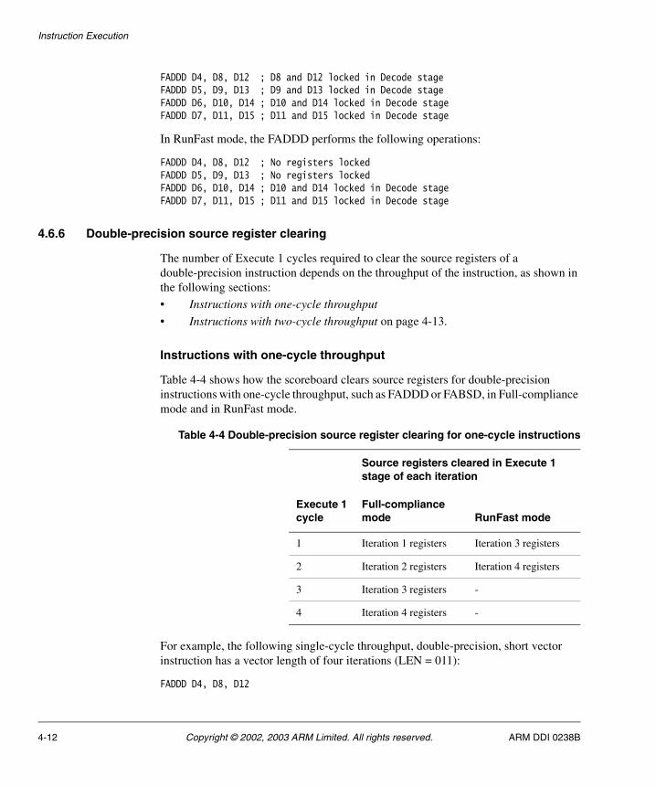
Instruction Execution
FADDD D4, D8, D12 ; D8 and D12 locked in Decode stageFADDD D5, D9, D13 ; D9 and D13 locked in Decode stageFADDD D6, D10, D14 ; D10 and D14 locked in Decode stageFADDD D7, D11, D15 ; D11 and D15 locked in Decode stage
In RunFast mode, the FADDD performs the following operations:
FADDD D4, D8, D12 ; No registers lockedFADDD D5, D9, D13 ; No registers lockedFADDD D6, D10, D14 ; D10 and D14 locked in Decode stageFADDD D7, D11, D15 ; D11 and D15 locked in Decode stage
4.6.6 Double-precision source register clearing
The number of Execute 1 cycles required to clear the source registers of a double-precision instruction depends on the throughput of the instruction, as shown in the following sections:
• Instructions with one-cycle throughput
• Instructions with two-cycle throughput on page 4-13.
Instructions with one-cycle throughput
Table 4-4 shows how the scoreboard clears source registers for double-precision instructions with one-cycle throughput, such as FADDD or FABSD, in Full-compliance mode and in RunFast mode.
For example, the following single-cycle throughput, double-precision, short vector instruction has a vector length of four iterations (LEN = 011):
FADDD D4, D8, D12
Table 4-4 Double-precision source register clearing for one-cycle instructions
Execute 1cycle
Source registers cleared in Execute 1 stage of each iteration
Full-compliance mode RunFast mode
1 Iteration 1 registers Iteration 3 registers
2 Iteration 2 registers Iteration 4 registers
3 Iteration 3 registers -
4 Iteration 4 registers -
4-12 Copyright © 2002, 2003 ARM Limited. All rights reserved. ARM DDI 0238B

Instruction Execution
In Full-compliance mode, the FADDD locks all source registers in the Decode stage and clears the source registers in the following Execute 1 cycles:
FADDD D4, D8, D12 ; D8 and D12 cleared in 1st Execute 1 cycleFADDD D5, D9, D13 ; D9 and D13 cleared in 2nd Execute 1 cycleFADDD D6, D10, D14 ; D10 and D14 cleared in 3rd Execute 1 cycleFADDD D7, D11, D15 ; D11 and D15 cleared in 4th Execute 1 cycle
In RunFast mode, the FADDD locks the source registers for only the third and fourth iterations in the Decode stage. It clears the source registers for the third iteration in the first Execute 1 cycle of the instruction and the source registers for the fourth iteration in the second Execute 1 cycle:
FADDD D4, D8, D12 ; No registers locked for this iteration, none to be clearedFADDD D5, D9, D13 ; No registers locked for this iteration, none to be clearedFADDD D6, D10, D14 ; D10 and D14 cleared in 1st Execute 1 cycleFADDD D7, D11, D15 ; D11 and D15 cleared in 2nd Execute 1 cycle
Instructions with two-cycle throughput
Table 4-5 shows how the scoreboard clears source registers for double-precision instructions with two-cycle throughput, such as FMULD or FMACD, in Full-compliance mode and in RunFast mode.
Table 4-5 Double-precision source register clearing for two-cycle instructions
Execute 1cycle
Source registers cleared in Execute 1 stage of each iteration
Full-compliance mode RunFast mode
1 Iteration 1 registers Iteration 3 registers
2 - -
3 Iteration 2 registers Iteration 4 registers
4 - -
5 Iteration 3 registers -
6 - -
7 Iteration 4 registers -
8 - -
ARM DDI 0238B Copyright © 2002, 2003 ARM Limited. All rights reserved. 4-13

Instruction Execution
For example, the following two-cycle throughput, double-precision, short vector instruction has a vector length of four iterations (LEN = 011):
FMULD D4, D8, D12
In Full-compliance mode, the FMULD locks all source registers in the Decode stage and clears the source registers in the following operations:
FMULD D4, D8, D12 ; D8 and D12 cleared in 1st Execute 1 cycleFMULD D5, D9, D13 ; D9 and D13 cleared in 3rd Execute 1 cycleFMULD D6, D10, D14 ; D10 and D14 cleared in 5th Execute 1 cycleFMULD D7, D11, D15 ; D11 and D15 cleared in 7th Execute 1 cycle
In RunFast mode, the FMULD locks the source registers for only the third and fourth iterations in the Decode stage. It clears the source registers for the third iteration in the first Execute 1 cycle of the instruction and the source registers for the fourth iteration in the third Execute 1 cycle:
FMULD D4, D8, D12 ; No registers locked for this iteration, none to be clearedFMULD D5, D9, D13 ; No registers locked for this iteration, none to be clearedFMULD D6, D10, D14 ; D10 and D14 cleared in 1st Execute 1 cycleFMULD D7, D11, D15 ; D11 and D15 cleared in 3rd Execute 1 cycle
4.6.7 Data hazards in Full-compliance mode
Source registers must be protected in the event of an exceptional condition in an instruction or in an iteration of a short vector instruction.
Source registers are cleared in the first Execute 1 cycle of an operation. To enable forwarding to a subsequent instruction, destination registers are cleared in the next-to-last cycle.
The sections that follow give examples of data hazards in RunFast mode:
• Status register RAW hazard example
• Load multiple/CDP RAW hazard example on page 4-15
• CDP/CDP RAW hazard example on page 4-16
• Load multiple/short vector CDP RAW hazard example on page 4-16
• Short vector CDP/store RAR hazard example on page 4-17
• Short vector CDP/load multiple WAR hazard example on page 4-17.
Status register RAW hazard example
In Example 4-5 on page 4-15, the FMSTAT is stalled for three cycles in the Fetch stage until the FCMPS updates the condition codes in the FPSCR register. Two cycles later, FMSTAT updates the ARM CPSR register with the condition codes.
4-14 Copyright © 2002, 2003 ARM Limited. All rights reserved. ARM DDI 0238B

Instruction Execution
Example 4-5 Status register RAW hazard
FCMPS S1, S2FMSTAT
Table 4-6 shows the VFP9-S pipeline stages for Example 4-5.
Load multiple/CDP RAW hazard example
In Example 4-6, the FADDS is stalled in the Fetch stage for nine cycles until the FLDM makes its last transfer to the VFP9-S coprocessor.
Example 4-6 Load multiple/CDP RAW hazard
FLDM [Rx], {S8-S15}FADDS S1, S2, S15
Table 4-7 shows the VFP9-S pipeline stages for Example 4-6.
Table 4-6 Pipeline stages for Example 4-5
Instruction cycle number
Instruction 1 2 3 4 5 6 7 8 9 10
FCMPS F D E1 E2 E3 E4 - - - -
FMSTAT - F F F F F D E M W
Table 4-7 Pipeline stages for Example 4-6
Instruction cycle number
Instruction 1 2 3 4 5 6 7 8 9 10 11 12 13 14 15 16
FLDM F D E M W W W W W W W W - - - -
FADDS - F F F F F F F F F F D E1 E2 E3 E4
ARM DDI 0238B Copyright © 2002, 2003 ARM Limited. All rights reserved. 4-15

Instruction Execution
CDP/CDP RAW hazard example
In Example 4-7 on page 4-16, the FADDS is stalled for three cycles in the Fetch stage until the FMULS data is written and forwarded in cycle 6 to the Decode stage of the FADDS.
Example 4-7 CDP/CDP RAW hazard
FMULS S4, S1, S0FADDS S5, S4, S3
Table 4-8 shows VFP9-S pipeline stages of Example 4-7.
Load multiple/short vector CDP RAW hazard example
In Example 4-8, the short vector FADDS is stalled in the Fetch stage until the FLDM loads all source registers required by the FADDS. In this case, the FADDS is stalled for two cycles. It does not have to wait for completion of the FLDM, because it depends on the FLDM only for one register, S7. The S7 data is forwarded in cycle 5. The vector length is four iterations (LEN = 3), and the stride is one (STRIDE = 0). Notice that the first source vector uses registers S7, S0, S1, and S2, and the only FADDS source register loaded by the FLDM is S7. This example is based on the assumption that the remaining source and destination registers are available to the FADDS in cycle 5.
Example 4-8 Load multiple/short vector CDP RAW hazard
FLDM [R2], {S7-S14}FADDS S16, S7, S25
Table 4-8 Pipeline stages for Example 4-7
Instruction cycle number
Instruction 1 2 3 4 5 6 7 8 9 10
FMULS F D E1 E2 E3 E4 - - - -
FADDS - F F F F D E1 E2 E3 E4
4-16 Copyright © 2002, 2003 ARM Limited. All rights reserved. ARM DDI 0238B
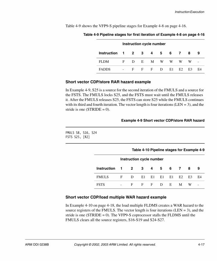
Instruction Execution
Table 4-9 shows the VFP9-S pipeline stages for Example 4-8 on page 4-16.
Short vector CDP/store RAR hazard example
In Example 4-9, S25 is a source for the second iteration of the FMULS and a source for the FSTS. The FMULS locks S25, and the FSTS must wait until the FMULS releases it. After the FMULS releases S25, the FSTS can store S25 while the FMULS continues with its third and fourth iteration. The vector length is four iterations (LEN = 3), and the stride is one (STRIDE = 0).
Example 4-9 Short vector CDP/store RAR hazard
FMULS S8, S16, S24FSTS S25, [R2]
Short vector CDP/load multiple WAR hazard example
In Example 4-10 on page 4-18, the load multiple FLDMS creates a WAR hazard to the source registers of the FMULS. The vector length is four iterations (LEN = 3), and the stride is one (STRIDE = 0). The VFP9-S coprocessor stalls the FLDMS until the FMULS clears all the source registers, S16-S19 and S24-S27.
Table 4-9 Pipeline stages for first iteration of Example 4-8 on page 4-16
Instruction cycle number
Instruction 1 2 3 4 5 6 7 8 9
FLDM F D E M W W W W -
FADDS - F F F D E1 E2 E3 E4
Table 4-10 Pipeline stages for Example 4-9
Instruction cycle number
Instruction 1 2 3 4 5 6 7 8 9
FMULS F D E1 E1 E1 E1 E2 E3 E4
FSTS - F F F D E M W -
ARM DDI 0238B Copyright © 2002, 2003 ARM Limited. All rights reserved. 4-17

Instruction Execution
Example 4-10 Short vector CDP/load multiple WAR hazard
FMULS S8, S16, S24FLDMS [R2], {S16-S27}
4.6.8 Data hazards in RunFast mode
In RunFast mode, source registers are locked when the vector length exceeds four iterations in single-precision instructions or two iterations in double-precision instructions. When the vectors are sufficiently short, no hazards exist involving the source registers.
The sections that follow give examples of data hazards in Full-compliance mode:
• Short vector CDP/store RAR hazard example
• Short vector CDP/load multiple WAR hazard example on page 4-19.
Short vector CDP/store RAR hazard example
In Example 4-11, the vector length is four iterations (LEN = 3), and the stride is one (STRIDE = 0). This is the same example as Short vector CDP/store RAR hazard on page 4-17. Executing these instructions in RunFast mode reduces the cycle count of the FSTS by one cycle.
Example 4-11 RAR hazard eliminated by RunFast mode
FMULS S8, S16, S24FSTS S25, [R2]
Table 4-11 Pipeline stages for first iteration of Example 4-10
Instruction cycle number
Instruction 1 2 3 4 5 6 7 8 9 10 11 12 13 14 15 16 17
FMULS F D E1 E1 E1 E1 E2 E3 E4 - - - - - - - -
FLDMS - F F F F F D E M W W W W W W W W
4-18 Copyright © 2002, 2003 ARM Limited. All rights reserved. ARM DDI 0238B

Instruction Execution
Table 4-12 shows that the VFP9-S coprocessor does not stall the store, which can begin execution in cycle 4.
Short vector CDP/load multiple WAR hazard example
In Example 4-12, the vector length is four iterations (LEN = 3), and the stride is one (STRIDE = 0). This is the same example as Short vector CDP/load multiple WAR hazard on page 4-18. Executing these instructions in RunFast mode reduces the cycle count of the FLDMS by three cycles.
Example 4-12 WAR hazard eliminated by RunFast mode
FMULS S8, S16, S24FLDMS [R2], {S16-S27}
Table 4-13 shows that the VFP9-S coprocessor does not stall the FLDM operation.
4.6.9 Resource hazards
Resource hazards are possible in the following cases:
• Following a load or store operation, the ARM9E processor stalls load, store, and CDP instructions until the first load or store operation clears the Execute stage of the ARM LS pipeline.
Table 4-12 Pipeline stages for Example 4-11 on page 4-18
Instruction cycle number
Instruction 1 2 3 4 5 6 7 8 9
FMULS F D E1 E1 E1 E1 E2 E3 E4
FSTS - F F D E M W - -
Table 4-13 Pipeline stages for Example 4-12
Instruction cycle number
Instruction 1 2 3 4 5 6 7 8 9 10
FMULS F D E1 E1 E1 E1 E2 E3 E4 -
FLDM - F F D E M W W W W
ARM DDI 0238B Copyright © 2002, 2003 ARM Limited. All rights reserved. 4-19
Instruction Execution
• An arithmetic instruction following a short vector arithmetic instruction or a double-precision multiply or multiply and accumulate instruction can be stalled due to instruction latency. The latency of double-precision multiply and multiply and accumulate instructions is two cycles, causing a one-cycle stall for arithmetic instructions that follow immediately.
• A single-precision divide or square root instruction stalls the DS pipeline for 13 cycles. A double-precision divide or square root instruction stalls the DS pipeline for 27 cycles. A scalar divide or square root instruction does not stall CDP instructions in the FMAC pipeline.
• A short vector divide or square root instruction of length greater than one iteration stalls all subsequent CDP operations. The stall ends when the final iteration of the short vector instruction completes the first Execute 1 stage for that iteration.
The VFP9-S LS pipeline is completely separate from the VFP9-S FMAC and DS pipelines. No resource hazards exist between data transfer instructions and arithmetic instructions.
In the ARM9E processor, the load and store pipeline is shared with the arithmetic pipeline. As a result, load and store multiple instructions and memory transfers with memory access greater than one cycle stall all subsequent instructions during the transfer. This is shown in the following sequence of instructions:
FLDMS [Rx], {S0-S7}FADDS S8, S9, S10
The ARM9E processor stalls the FADDS in the ARM Execute stage until the FLDMS receives the data from memory or cache and progresses to the next-to-last ARM Writeback stage.
In the following sequence, the order is reversed:
FADDS S8, S9, S10FLDMS [Rx], {S0-S7}
The FLDMS begins executing in the cycle following the issue of the FADDS, in parallel with the FADDS. This is also the behavior even when the FADDS is a short vector instruction, because the ARM9E processor treats short vector instructions as single-cycle instructions regardless of the number of iterations. VFP9-S coprocessor performance can be significantly increased by issuing short vector instructions before load or store instructions.
The sections that follow give examples of resource hazards:
• Load multiple/load/CDP resource hazard example on page 4-21
• Load multiple/CDP/CDP resource hazard example on page 4-21
• CDP/CDP resource hazard example on page 4-22.
4-20 Copyright © 2002, 2003 ARM Limited. All rights reserved. ARM DDI 0238B

Instruction Execution
Load multiple/load/CDP resource hazard example
In Example 4-13, the FLDM is executing three transfers to the VFP9-S coprocessor. The FLDS is stalled behind the FLDM until the FLDM enters the final Execute cycle. The FADDS is stalled until the FLDS enters the Execute cycle. This example demonstrates the operation of the ARM LS pipeline and its effect on the VFP9-S pipeline.
Example 4-13 FLDM-FLDS-FADDS resource hazard
FLDM [R2], {S8-S10}FLDS [R4], S16 FADDS S2, S3, S4
Table 4-14 shows the pipeline stages for Example 4-13.
Load multiple/CDP/CDP resource hazard example
In Example 4-14, a resource hazard exists for the FMULS due to the FLDM in the prior cycle. The FMULS stalls in the ARM9E pipeline until the FLDM completes the last Execute cycle
The scalar FADDS after the vector FMULS also has a resource hazard. The FADDS stalls in the VFP9-S Fetch stage for four cycles until the short vector FMULS enters the Execute 1 stage for the final iteration. No data hazard exists between the FLDM and the FMULS. The vector length is four iterations (LEN = 3), and the stride is one (STRIDE = 0).
Example 4-14 Load multiple /CDP/CDP resource hazard
FLDM [R2], {S8-S10}
Table 4-14 Pipeline stages for Example 4-13
Instruction cycle number
Instruction 1 2 3 4 5 6 7 8 9 10 11 12
FLDM F D E M W W W - - - - -
FLDS - F F F F D E M W - - -
FADDS - - - - - F F D E1 E2 E3 E4
ARM DDI 0238B Copyright © 2002, 2003 ARM Limited. All rights reserved. 4-21

Instruction Execution
FMULS S16, S24, S4FADDS S1, S20, S21
Table 4-15 shows the pipeline stages for Example 4-14 on page 4-21.
CDP/CDP resource hazard example
In Example 4-15, a short vector divide with a length of two iterations (LEN = 1) is followed by a FADDS instruction. The short vector divide requires the Execute 1 stage of the FMAC pipeline for the first cycle of each iteration of the divide, resulting in a stall of the FADDS until the final iteration of the divide enters the first Execute 1 cycle. The divide iterates for 13 cycles in the Execute 1/Execute 2 stages of the divider, shown in Table 4-16 as E1. The first and shared Execute 1 cycle for each divide iteration is designated as E1’.
Example 4-15 CDP/CDP resource hazard
FDIVS S8, S10, S12FADDS S0, S0, S1
Table 4-16 shows the pipeline stages for Example 4-15.
Table 4-15 Pipeline stages for Example 4-14 on page 4-21
Instruction cycle number
Instruction 1 2 3 4 5 6 7 8 9 10 11 12 13
FLDM F D E M W W W - - - - - - -
FMULS - F F F F D E1 E1 E1 E1 E2 E3 E4 -
FADDS - - - - - F F F F D E1 E2 E3 E4
Table 4-16 Pipeline stages for Example 4-15
Instruction cycle number
Instruction 1 2 3 4 . . . 14 15 16 17 18 19 20 21 . . . 28 29 30 31
FDIVS F D E1’ E1 E1 E1 E1 E1’ E1 E1 E1 E1 E1 E1 E1 E2 E3 E4
FADDS - - F F F F F D F E1 E2 E3 E4 - - - - -
4-22 Copyright © 2002, 2003 ARM Limited. All rights reserved. ARM DDI 0238B

Instruction Execution
4.7 Parallel execution
Separate LS, FMAC, and DS pipelines allow for parallel operation of CDP and load and store instructions. Scheduling instructions to take advantage of the parallelism can result in a significant improvement in program execution time.
An instruction begins execution when the following are true:
• no data hazards or control hazards exist
• there are no pending iterations of a short vector or multiple instruction in the instruction’s pipeline
• there is no incomplete load or store operation in the ARM9E pipeline.
The ARM9E processor completes execution of a load or store multiple instruction before another instruction can be issued. As a result, algorithms that use load or store multiples can improve performance by issuing CDP instructions before the load or store multiple.
A load or store instruction begins execution when the following are true:
• the instruction can be issued by the ARM9E processor
• there is no data or control hazard with any currently executing instructions
• the LS pipeline is not currently stalled or busy with a load or store multiple instruction.
A CDP instruction can be issued to the FMAC pipeline when the following are true:
• the instruction can be issued by the ARM9E processor
• a load or store multiple instruction is not executing
• a load instruction is not stalled waiting for data
• there is no data or control hazard with any currently executing operations
• the FMAC pipeline is available. It might be unavailable if a short vector CDP is executing or if a double-precision multiply is in the first cycle of the multiply operation
• no short vector instruction is executing in either the FMAC or DS pipeline.
A divide or square root instruction can be issued to the DS pipeline if:
• the instruction can be issued by the ARM9E processor
• a load or store multiple instruction is not executing
ARM DDI 0238B Copyright © 2002, 2003 ARM Limited. All rights reserved. 4-23

Instruction Execution
• a load instruction is not stalled waiting for data
• there is no data or control hazard with any currently executing instructions
• no short vector operation is executing in the FMAC pipeline
• the DS pipeline is available. It might be unavailable if a divide or square root is executing in the DS pipeline Execute 1 stage.
4.7.1 An example of parallel execution
The VFP9-S pipelines are capable of parallel and independent execution without blocking issue or writeback from any pipeline. Example 4-16 shows:
• a scalar divide in the DS pipeline
• a short vector add in the FMAC pipeline
• a load multiple in the LS pipeline.
In Example 4-16, the vector length is four iterations (LEN = 3), and the stride is one (STRIDE = 0).
Example 4-16 Parallel execution in all three pipelines
FDIVS S0, S1, S2FADDS S16, S20, S24FLDM [R4], {S4-S8}
Table 4-17 shows the pipeline stages for Example 4-16. The first and shared Execute 1 cycle for the divide is designated as E1’.
When all previous data hazards and resource hazards are removed, the instructions are issued to the VFP9-S every other cycle. No data hazards exist between the three instructions in Example 4-16. The FDIVS destination is in bank 0, so the operation is
Table 4-17 Pipeline stages for Example 4-16
Instruction cycle number
1 2 3 4 5 6 7 8 9 10 11 12 13 14 15 16 17
FDIVS F D E1’ E1 E1 E1 E1 E1 E1 E1 E1 E1 E1 E1 E1 E1 E2
FADDS - F F D E1 E1 E1 E1 E2 E3 E4 - - - - - -
FLDM - - - F F D E M W W W W W - - - -
4-24 Copyright © 2002, 2003 ARM Limited. All rights reserved. ARM DDI 0238B

Instruction Execution
scalar regardless of the LEN value in the FPSCR register. Divide and square root instructions require one cycle in the FMAC Execute 1 stage. In this example, cycle 3 uses both the FMAC and DS Execute 1 stages. Subsequent divide cycles require only the DS Execute 1 and Execute 2 stages, and the FMAC Execute 1 stage is available. If the FDIVS were a short vector instruction, the FADDS would not begin execution until the last iteration of the FDIVS passed the first Execute 1 stage. The FADDS is a short vector instruction and requires the FMAC Execute 1 stage for cycles 5–8. To the ARM9E processor, the vector FADDS operation appears as a single-cycle instruction regardless of the number of VFP9-S iterations. If there are no stalls due to memory latency, the FLDM begins execution in cycle 4 and starts transferring data to the VFP9-S coprocessor in cycle 9. The presence of the FLDM in the ARM9E processor pipeline causes subsequent operations to stall until cycle 11, when the ARM Execute stage is no longer required by the FLDM. In cycle 11, another ARM or VFP instruction can enter the Execute stage.
ARM DDI 0238B Copyright © 2002, 2003 ARM Limited. All rights reserved. 4-25

Instruction Execution
4.8 Execution timing
The VFP9-S instruction cycle counts in Table 4-18 are provided as a guide and not as a substitute for running the code on a system or cycle-accurate simulator. Also, the execution of VFP9-S instructions depends on the execution of the instruction in the ARM9E processor, and stall and memory access issues directly affect performance of VFP9-S code. For information on instruction timing within the ARM9E processor, see the Technical Reference Manual for the ARM9E processor that you are using.
In Table 4-18, throughput is defined as the cycle after issue in which another instruction can begin execution. Instruction latency is the number of cycles after which the data is available for another operation. Forwarding reduces the latency by one cycle for operations dependent on floating-point data.
Note
FMXR and FMRX are serializing instructions. Their latency depends on the register transferred and the current activity in the VFP9-S coprocessor when the instruction is issued.
Table 4-18 shows the throughput and latency for all VFP9-S CDP instructions.
Table 4-18 Throughput and latency cycle counts for VFP9-S CDP instructions
Instructions
Single-precision Double-precision
Throughput Latency Throughput Latency
FADD, FSUB, FABS, FNEG, FCVT, FCPY
1 4 1 4
FCMP, FCMPE, FCMPZ, FCMPEZ
1 4 1 4
FSITO, FUITO, FTOSI, FTOUI, FTOUIZ, FTOSIZ
1 4 1 4
FMUL, FNMUL 1 4 2 5
FMAC, FNMAC, FMSC, FNMSC
1 4 2 5
FDIV, FSQRT 14 17 28 31
FLDa 1 4 2 5
FSTab 1 3 2 4
4-26 Copyright © 2002, 2003 ARM Limited. All rights reserved. ARM DDI 0238B
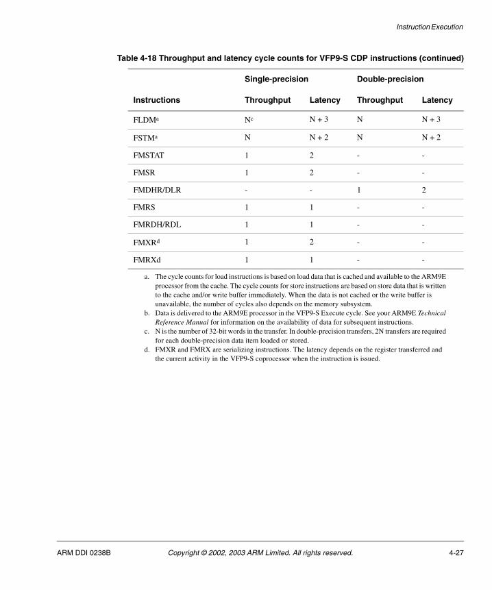
Instruction Execution
FLDMa Nc N + 3 N N + 3
FSTMa N N + 2 N N + 2
FMSTAT 1 2 - -
FMSR 1 2 - -
FMDHR/DLR - - 1 2
FMRS 1 1 - -
FMRDH/RDL 1 1 - -
FMXRd 1 2 - -
FMRXd 1 1 - -
a. The cycle counts for load instructions is based on load data that is cached and available to the ARM9E processor from the cache. The cycle counts for store instructions are based on store data that is written to the cache and/or write buffer immediately. When the data is not cached or the write buffer is unavailable, the number of cycles also depends on the memory subsystem.
b. Data is delivered to the ARM9E processor in the VFP9-S Execute cycle. See your ARM9E Technical Reference Manual for information on the availability of data for subsequent instructions.
c. N is the number of 32-bit words in the transfer. In double-precision transfers, 2N transfers are required for each double-precision data item loaded or stored.
d. FMXR and FMRX are serializing instructions. The latency depends on the register transferred and the current activity in the VFP9-S coprocessor when the instruction is issued.
Table 4-18 Throughput and latency cycle counts for VFP9-S CDP instructions (continued)
Instructions
Single-precision Double-precision
Throughput Latency Throughput Latency
ARM DDI 0238B Copyright © 2002, 2003 ARM Limited. All rights reserved. 4-27

Instruction Execution
4-28 Copyright © 2002, 2003 ARM Limited. All rights reserved. ARM DDI 0238B

Chapter 5 Exception Handling
This chapter describes VFP9-S exception processing. It contains the following sections:
• About exception processing on page 5-2
• Support code on page 5-3
• Illegal instructions on page 5-6
• Determination of the trigger instruction on page 5-7
• Input Subnormal exception on page 5-12
• Invalid Operation exception on page 5-13
• Division-by-Zero exception on page 5-16
• Overflow exception on page 5-17
• Underflow exception on page 5-19
• Inexact exception on page 5-21
• Input exceptions on page 5-22
• Arithmetic exceptions on page 5-23.
ARM DDI 0238B Copyright © 2002, 2003 ARM Limited. All rights reserved. 5-1

Exception Handling
5.1 About exception processing
The VFP9-S coprocessor handles exceptions imprecisely with respect to both the state of the ARM processor and the state of the VFP9-S coprocessor. It detects an exceptional instruction after the instruction passes the point for exception handling in the ARM processor. It then enters the exceptional state and signals the presence of an exception by refusing to accept a subsequent VFP instruction. The instruction that triggers exception handling bounces to the ARM processor. The bounced instruction is not necessarily the instruction immediately following the exceptional instruction. Depending on sequence of instructions that follow, the bounce can occur several instructions later.
The VFP9-S coprocessor can generate exceptions only on arithmetic operations and not on data transfer operations. Instructions that involve copying data between VFP9-S registers are nonarithmetic and cannot produce exceptions. These are FCPY, FABS, and FNEG. These instructions copy NaNs and subnormal operands without bouncing. NaNs retain all fraction bits regardless of the state of the DN bit, FPSCR[25]. SNaNs do not cause an Invalid Operation exception. Subnormal operands are not flushed to zero regardless of the state of the FZ bit, FPSCR[24].
In both Full-compliance and RunFast modes, the VFP9-S hardware, with support code, processes exceptions according to the IEEE 754 standard. VFP9-S exception processing includes calling user trap handlers with intermediate operands specified by the IEEE 754 standard.
For descriptions of each of the exception flags and their bounce characteristics, see the sections Invalid Operation exception on page 5-13 to Arithmetic exceptions on page 5-23.
5-2 Copyright © 2002, 2003 ARM Limited. All rights reserved. ARM DDI 0238B

Exception Handling
5.2 Support code
The VFP9-S coprocessor provides floating-point functionality through a combination of hardware and software support. Normally, the VFP9-S hardware executes floating-point instructions completely in hardware. However, the VFP9-S coprocessor can, under certain circumstances, refuse to accept a floating-point instruction, causing the ARM Undefined Instruction exception. This is known as bouncing the instruction.
There are two main reasons for bouncing an instruction:
• potential floating-point arithmetic exceptions
• illegal instructions.
When an instruction bounces, software installed on the ARM Undefined instruction vector determines why the VFP9-S coprocessor rejected the instruction and takes appropriate remedial action. This software is called the VFP support code. The support code has two components:
• a library of routines that perform floating-point arithmetic functions
• a set of exception handlers that process exceptional conditions.
See AFS Firmware Suite Reference Guide for details of support code.
5.2.1 Bounced instructions
When an exception occurs, the VFP9-S hardware sets the EX flag, FPEXC[31], and loads the FPINST register with a copy of the potentially exceptional instruction. The VFP9-S coprocessor is now in the exceptional state. The instruction that bounces as a result of the exceptional state is referred to as the trigger instruction. When in the exceptional state, the VFP9-S coprocessor bounces either the instruction currently in the VFP9-S Fetch stage or the next VFP instruction issued. Some instructions cannot be trigger instructions. For example, an FMRX of the FPEXC register returns the FPEXC register and does not bounce. See Determination of the trigger instruction on page 5-7.
An instruction bounce always occurs when there is an enabled floating-point exception. The hardware detects potential exceptions pessimistically. This means that it can also bounce instructions when there is no floating-point exception present. This occurs in some rare cases when it detects only a potential for an exception in the Execute 1 stage.
The remedial action is performed as follows:
1. The support code starts by reading the FPEXC register. If the EX flag, FPEXC[31], is set, a potential exception is present. If not, an illegal instruction is detected. See Illegal instructions on page 5-6.
ARM DDI 0238B Copyright © 2002, 2003 ARM Limited. All rights reserved. 5-3

Exception Handling
2. The support code writes to the FPEXC register to clear the EX flag. Failure to do this can result in an infinite loop of exceptions when the support code next accesses the VFP9-S hardware.
3. The support code reads the FPINST register to determine the instruction that caused the potential exception.
4. The support code decodes the instruction in the FPINST register, reads its operands, including implicit information such as the rounding mode and vector length in the FPSCR register, executes the operation, and determines whether a floating-point exception occurred.
5. If no floating-point exception occurred, the support code writes the correct result of the operation and sets the appropriate flags in the FPSCR register.
If one or more floating-point exceptions occurred, but all of them were disabled, the support code determines the correct result of the instruction, writes it to the destination register, and sets the corresponding flags in the FPSCR register.
If one or more floating-point exceptions occurred, and at least one of them was enabled, the support code computes the intermediate result specified by the IEEE 754 standard, if required, and calls the user trap handler for that exception. The user trap handler can provide a result for the instruction and continue program execution, generate a signal or message to the operating system or the user, or simply terminate the program.
6. If the potentially exceptional instruction specified a short vector operation, the hardware does not execute any vector iterations after the one that encountered the potentially exceptional condition. The support code repeats steps 4 and 5 for any such iterations. See Exception processing for CDP short vector instructions on page 5-8 for more details.
7. If the FP2V flag, FPEXC[28], is set, the FPINST2 register contains another VFP instruction that was issued between the potentially exceptional instruction and the trigger instruction. This instruction is executed by the support code in the same manner as the instruction in the FPINST register. See Instruction registers, FPINST and FPINST2 on page 3-23 for more on FPINST2.
8. The support code finishes processing the potentially exceptional instruction and returns to the program containing the trigger instruction. The ARM processor refetches the trigger instruction from memory and reissues it to the VFP9-S coprocessor. Unless another bounce occurs, the trigger instruction is executed. Returning in this fashion is called retrying the trigger instruction.
The support code can be written to use the VFP9-S hardware for its internal calculations, provided that:
• recursive bounces are prevented or handled correctly
5-4 Copyright © 2002, 2003 ARM Limited. All rights reserved. ARM DDI 0238B

Exception Handling
• care is taken to restore the state of the original program before returning to it.
Restoring the state of the original program can be difficult if the original program was executing in FIQ mode or in Undefined instruction mode. It is legitimate for support code to disallow or restrict the use of VFP9-S instructions in these two processor modes.
ARM DDI 0238B Copyright © 2002, 2003 ARM Limited. All rights reserved. 5-5

Exception Handling
5.3 Illegal instructions
If there is not a potential floating-point exception from an earlier instruction, the current instruction can still be bounced if it is architecturally Undefined in some way. When this happens, the EX flag, FPEXC[31], is not set. The instruction that caused the bounce is contained in the memory word pointed to by r14_undef - 4.
It is possible that both conditions for an instruction to be bounced occur simultaneously. This happens when an illegal instruction is encountered and there is also a potential floating-point exception from an earlier instruction. When this happens, the EX flag is set, and the support code processes the potential exception in the earlier instruction. If and when it returns, it causes the illegal instruction to be retried and the sequence of events described in the paragraph above occurs.
The following instruction types are architecturally Undefined:
• instructions with opcode bit combinations defined as reserved in the architecture specification
• load or store instructions with Undefined P, W, and U bit combinations
• FMRX/FMXR instructions to or from a control register that is not defined
• User mode FMRX/FMXR instructions to or from a control register that can be accessed only in a privileged mode.
Certain instruction types do not have architecturally-defined behavior and can cause the ARM Undefined Instruction trap to be entered. They might be treated as illegal instructions by some implementations of the VFP, but this cannot not be relied on. These instruction types are:
• Load or store multiple instructions with a transfer count of zero or greater than 32. In this VFP9-S implementation, these instructions are bounced.
• A short vector instruction with a combination of precision, length, and stride that causes the vector to wrap around and make more than one access to the same register. In this VFP9-S implementation, such an instruction bounces.
• A short vector instruction with overlapping source and destination register addresses that are not exactly the same. In this VFP9-S implementation, such an instruction does not bounce, and the results are Unpredictable.
5-6 Copyright © 2002, 2003 ARM Limited. All rights reserved. ARM DDI 0238B

Exception Handling
5.4 Determination of the trigger instruction
The ARM coprocessor interface specifies that an exceptional instruction that bounces to support code must signal on a subsequent coprocessor instruction. This is known as imprecise exception handling. It means that when the exception is processed, the VFP9-S and ARM user states might be different from their states when the exceptional instruction executed. Parallel execution of VFP9-S CDP instructions and load or store instructions allows the VFP9-S and ARM register files and memory to be modified outside of the program order.
The issue timing of VFP9-S instructions affects the determination the trigger instruction. The last iteration of a short vector CDP can be followed in the next cycle by a second CDP instruction. If there is no hazard, the VFP9-S coprocessor accepts the second CDP instruction before the exception status of the last iteration of the short vector CDP is known. The second CDP instruction is in the pretrigger slot and is retained in the FPINST2 register for the support code.VFP9-S.
Instruction fetch timing determines which instruction is the trigger instruction. A CDP instruction gets to the Execute 1 stage before a potential exceptional is detected. Meanwhile, the next VFP9-S instruction fetched is processed by the ARM processor and cannot cause an Undefined Instruction exception to be taken. This VFP9-S instruction is in the pretrigger slot and is retained for the support code in the FPINST2 register.
Several rules determine which instruction is the trigger instruction:
• An instruction that accesses an exception register, FPEXC, FPINST, or FPINST2, or the system ID register, FPSID, is not a trigger instruction in a privileged mode.
• Any instruction that stalls in the Decode stage due to register or resource hazard is the trigger instruction.
• The first instruction issued at least two cycles after the exceptional condition has been detected is the trigger instruction.
• A load or store instruction that reaches the Execute stage is not the trigger instruction. There can be several of these if the short vector is sufficiently long, and the exception is detected on a later iteration.
5.4.1 Exception processing for CDP scalar instructions
When the VFP9-S coprocessor detects an exceptional scalar CDP instruction, it loads the FPINST register with the instruction word for the exceptional instruction and flags the condition in the FPEXC register. It blocks the exceptional instruction from further execution and completes any instructions currently executing in the FMAC and DS pipelines.
ARM DDI 0238B Copyright © 2002, 2003 ARM Limited. All rights reserved. 5-7
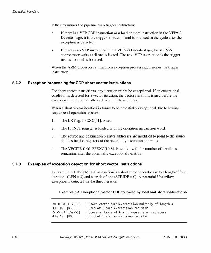
Exception Handling
It then examines the pipeline for a trigger instruction:
• If there is a VFP CDP instruction or a load or store instruction in the VFP9-S Decode stage, it is the trigger instruction and is bounced in the cycle after the exception is detected.
• If there is no VFP instruction in the VFP9-S Decode stage, the VFP9-S coprocessor waits until one is issued. The next VFP instruction is the trigger instruction and is bounced.
When the ARM processor returns from exception processing, it retries the trigger instruction.
5.4.2 Exception processing for CDP short vector instructions
For short vector instructions, any iteration might be exceptional. If an exceptional condition is detected for a vector iteration, the vector iterations issued before the exceptional iteration are allowed to complete and retire.
When a short vector iteration is found to be potentially exceptional, the following sequence of operations occurs:
1. The EX flag, FPEXC[31], is set.
2. The FPINST register is loaded with the operation instruction word.
3. The source and destination register addresses are modified to point to the source and destination registers of the potentially exceptional iteration.
4. The VECITR field, FPEXC[10:8], is written with the number of iterations remaining after the potentially exceptional iteration.
5.4.3 Examples of exception detection for short vector instructions
In Example 5-1, the FMULD instruction is a short vector operation with a length of four iterations (LEN = 3) and a stride of one (STRIDE = 0). A potential Underflow exception is detected on the third iteration.
Example 5-1 Exceptional vector CDP followed by load and store instructions
FMULD D8, D12, D8 ; Short vector double-precision multiply of length 4FLDD D0, [R5] ; Load of 1 double-precision registerFSTMS R3, {S2-S9} ; Store multiple of 8 single-precision registersFLDS S8, [R9] ; Load of 1 single-precision register
5-8 Copyright © 2002, 2003 ARM Limited. All rights reserved. ARM DDI 0238B

Exception Handling
A double-precision multiply requires two cycles in the Execute 1 stage, with exceptions detected in the first of the two cycles. The exception on the third iteration is detected in cycle 7. Before the FMULD exception is detected, the FLDD enters the Fetch stage in cycle 3, and the FSTMS enter the Fetch stage in cycle 5. The FLDD and the FSTMS complete execution and retire. The FLDS stalls in the Decode stage due to a resource conflict with the FSTMS and is the trigger instruction. It is bounced in cycle 9 and can be retried after exception processing. FPINST2 is invalid and the FP2V flag, FPEXC[28], is cleared.
After exception processing begins, the FPEXC register contains the following fields:
EX 1 The VFP9-S coprocessor is in the exceptional state.EN 1FP2V 0 FPINST2 does not contain a valid instruction.VECITR 000 One iteration remains after the exceptional iteration.INV 0UFC 1 Exception detected is a potential underflow.OFC 0IOC 0
The FPINST register contains the following fields. The conditional field and forced bits are not shown:
Op 0100 Multiply.Fd/D 1010/0 Destination of exceptional iteration is D10.Fm/M 1010/0 Fm source of exceptional iteration is D10.Fn/N 1110/0 Fn source of exceptional iteration is D14.CpID 1011 Operation is double-precision.
The FPINST2 register contains invalid data.
In Example 5-2 on page 5-10, the first FADDS is a vector operation with a length of two iterations (LEN = 1). A potential Invalid Operation exception is detected in the second iteration. The second FADDS progresses to the Decode stage and is captured in the
Table 5-1 Pipeline stages for Example 5-1 on page 5-8
Instruction cycle number
Instruction 1 2 3 4 5 6 7 8 9 10 11 12 13 14 15 16
FMULD D8, D12, D8 F D E1 E1 E1 E1 E1 E1 - - - - - - - -
FLDD D0, [R5] - F F D E M M W - - - - - - - -
FSTMS R3, {S2-S9} - - - F F D E M M M M M M M M W
FLDS S8, [R9] - - - - - F F D * - - - - - - -
ARM DDI 0238B Copyright © 2002, 2003 ARM Limited. All rights reserved. 5-9
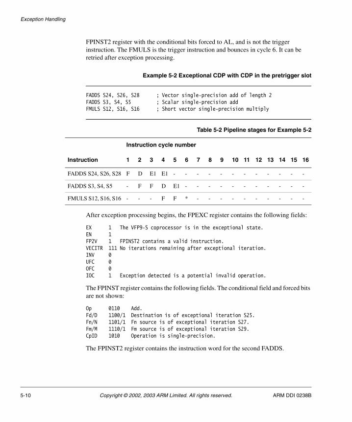
Exception Handling
FPINST2 register with the conditional bits forced to AL, and is not the trigger instruction. The FMULS is the trigger instruction and bounces in cycle 6. It can be retried after exception processing.
Example 5-2 Exceptional CDP with CDP in the pretrigger slot
FADDS S24, S26, S28 ; Vector single-precision add of length 2FADDS S3, S4, S5 ; Scalar single-precision addFMULS S12, S16, S16 ; Short vector single-precision multiply
After exception processing begins, the FPEXC register contains the following fields:
EX 1 The VFP9-S coprocessor is in the exceptional state.EN 1FP2V 1 FPINST2 contains a valid instruction.VECITR 111 No iterations remaining after exceptional iteration.INV 0UFC 0OFC 0IOC 1 Exception detected is a potential invalid operation.
The FPINST register contains the following fields. The conditional field and forced bits are not shown:
Op 0110 Add.Fd/D 1100/1 Destination is of exceptional iteration S25.Fn/N 1101/1 Fn source is of exceptional iteration S27.Fm/M 1110/1 Fm source is of exceptional iteration S29.CpID 1010 Operation is single-precision.
The FPINST2 register contains the instruction word for the second FADDS.
Table 5-2 Pipeline stages for Example 5-2
Instruction cycle number
Instruction 1 2 3 4 5 6 7 8 9 10 11 12 13 14 15 16
FADDS S24, S26, S28 F D E1 E1 - - - - - - - - - - - -
FADDS S3, S4, S5 - F F D E1 - - - - - - - - - - -
FMULS S12, S16, S16 - - - F F * - - - - - - - - - -
5-10 Copyright © 2002, 2003 ARM Limited. All rights reserved. ARM DDI 0238B

Exception Handling
In Example 5-3, FABSD is a short vector instruction with a length of four iterations (LEN = 3) and a stride of one (STRIDE = 0). It has a potential Overflow exception in the first iteration, detected in cycle 3. It is followed by an FMACS. The FMACS is stalled in the Decode stage waiting for the FABSD to exit the Execute 1 stage. The FMACS is the trigger instruction and can be retried after exception processing. FPINST2 is invalid and the FP2V flag is cleared.
Example 5-3 Exceptional vector CDP followed by scalar CDP with resourceconflict
FABSD D4, D12 ; Short vector double-precision absolute value of length 4FMACS S0, S3, S2 ; Scalar single-precision mac
After exception processing begins, the FPEXC register contain the following fields:
EX 1 The VFP9-S coprocessor is in the exceptional state.EN 1FP2V 0 FPINST2 does not contain a valid instruction.VECITR 010 Three iterations remain.INV 0UFC 0OFC 1 Exception detected is a potential overflow.IOC 0
The FPINST register contains the following fields. The conditional field and forced bits are not shown:
Op 1111 Extend.Fd/D 0100/0 Destination of exceptional iteration is D4.Fn/N 0000/1 Fn specifies FABS instruction.Fm/M 1100/0 Fm source is of exceptional iteration D12.CpID 1011 Operation is double-precision.
FPINST2 contains invalid data.
Table 5-3 Pipeline stages for Example 5-3
Instruction cycle number
Instruction 1 2 3 4 5 6 7 8 9 10 11 12 13 14 15 16
FABSD D4, D12 F D E1 - - - - - - - - - - - - -
FMACS S0, S3, S2 - F F D * - - - - - - - -
ARM DDI 0238B Copyright © 2002, 2003 ARM Limited. All rights reserved. 5-11

Exception Handling
5.5 Input Subnormal exception
The IDC flag, FPSCR[7], is set whenever an input operand is subnormal and the operation is not a float-to-integer conversion. The behavior of the VFP9-S coprocessor with a subnormal input operand is a function of the FZ bit, FPSCR[24]. If FZ is not set, the VFP9-S coprocessor bounces on the presence of a subnormal input. If FZ is set, the IDE bit, FPSCR[15], determines whether a bounce occurs.
5.5.1 Exception enabled
Setting the IDE bit enables Input Subnormal exceptions. An Input Subnormal exception sets the EX flag, FPEXC[31], and the IDC flag, FPSCR[7]. The source and destination registers for the instruction are unchanged in the VFP9-S register file.
5.5.2 Exception disabled
Clearing the IDE bit disables Input Subnormal exceptions. In Flush-to-Zero mode, the result of the operation, with the subnormal input replaced with a positive zero, is completed and written to the register file. Any appropriate flags in the FPSCR register are set.
When the VFP9-S coprocessor is not in Flush-to-Zero mode, any subnormal input causes a bounce to support code.
5-12 Copyright © 2002, 2003 ARM Limited. All rights reserved. ARM DDI 0238B

Exception Handling
5.6 Invalid Operation exception
An operation is invalid if the result cannot be represented, or if the result is not defined. In RunFast mode, the VFP9-S hardware processes all invalid instructions without support code intervention. In Full-compliance mode, only cases involving SNaNs require support code intervention.
Table 5-4 shows the operand combinations that produce Invalid Operation exceptions. In addition to the conditions in Table 5-4, any CDP instruction other than FCPY, FNEG, or FABS causes an Invalid Operation exception if one or more of its operands is an SNaN (see Table 3-1).
Table 5-4 Possible invalid Operation exceptions
Instruction Invalid Operation exceptions
FADD (+infinity) + (–infinity) or (–infinity) + (+infinity).
FSUB (+infinity) – (+infinity) or (–infinity) – (–infinity).
FMUL/FNMUL 0 × ±infinity or ±infinity × 0.In Flush-to-Zero mode, a subnormal input is treated as a positive zero for detecting an Invalid Operation exception
FDIV Zero/zero or infinity/infinity.
In Flush-to-Zero mode, a subnormal input is treated as a positive zero for detecting an Invalid Operation exception
FMAC/FNMAC Any condition that can cause an Invalid Operation exception for FMUL or FADD can cause an Invalid Operation exception for FMAC and FNMAC. The product generated by the FMAC or FNMAC multiply operation of is considered in the detection of the Invalid Operation exception for the subsequent sum operation.
FMSC/FNMSC Any of the conditions that can cause an Invalid Operation exception for FMUL or FSUB can cause an Invalid Operation exception for FMSC and FNMSC. The product generated by the FMSC or FNMSC multiply operation is considered in the detection of the Invalid Operation exception for the subsequent difference operation.
FSQRT Source is less than 0.
FTOUI Rounded result would lie outside the range 0 ≤ result < 232.
FTOSI Rounded result would lie outside the range –231 ≤ result < 231.
ARM DDI 0238B Copyright © 2002, 2003 ARM Limited. All rights reserved. 5-13

Exception Handling
5.6.1 Exception enabled
Setting the IOE bit, FPSCR[8], enables Invalid Operation exceptions. The VFP9-S coprocessor detects most Invalid Operations exceptions conclusively but some are detected pessimistically. The pessimistically detected operations are:
• FTOUI with a negative input. A small negative input might round to a zero, which is not an invalid condition.
• A float-to-integer conversion with a maximum exponent for the destination precision and any rounding mode other than round-toward-zero. The impact of rounding is unknown in the Execute 1 stage.
• An FMAC-family operation with an infinity in the A operand and a potential product overflow to an infinity.
When the VFP9-S coprocessor detects a pessimistic case, the EX flag, FPEXC[31], and the IOC flag, FPEXC[0], are set. The IOC flag in the FPSCR register, FPSCR[0], is not set by the hardware and must be set by the support code before calling the user trap handler.
The support code determines the exception status of the pessimistically bounced cases. If an invalid condition exists, the Invalid Operation exception user trap handler is called. The source and destination registers for the instruction are valid in the VFP9-S register file.
5.6.2 Exception disabled
If the IOE bit is not set, the VFP9-S coprocessor handles all invalid cases according to the IEEE 754 standard. The default NaN is written into the destination register for all operations except integer conversion operations.
Conversion of a floating-point value that is outside the range of the destination integer is an invalid condition rather than an overflow condition. When an invalid condition exists for a float-to-integer conversion, the VFP9-S coprocessor delivers a default result to the destination register and sets the IOC flag, FPSCR[0]. Table 5-5 on page 5-15 shows the default results for input values after rounding.
Note A negative input to an unsigned conversion that does not round to a true zero in the conversion process sets the IOC flag, FPEXC[0].
5-14 Copyright © 2002, 2003 ARM Limited. All rights reserved. ARM DDI 0238B

Exception Handling
Table 5-5 Default results for invalid conversion inputs
FTOUIS and FTOUID FTOSIS and FTOSID
Input valueafter rounding
ResultFPSCR IOCflag set?
ResultFPSCR IOCflag set?
x ≥ 232 0xFFFFFFFF Yes 0x7FFFFFFF Yes
231 ≤ x < 231 Integer No 0x7FFFFFFF Yes
0 ≤ x < 231 Integer No Integer No
0 > x ≥ ∠231 0x00000000 Yes Integer No
x < –231 0x00000000 Yes 0x80000000 Yes
ARM DDI 0238B Copyright © 2002, 2003 ARM Limited. All rights reserved. 5-15

Exception Handling
5.7 Division-by-Zero exception
The Division-by-Zero exception is generated for a division of x by zero, where x is anything other than a zero, infinity, or a NaN. In Flush-to-Zero mode, a subnormal input is treated as a positive zero for divide-by-zero detection. What happens depends on whether or not the Invalid Operation exception is enabled.
5.7.1 Exception enabled
If the DZE bit, FPSCR[9], is set, the division-by-zero user trap handler is called. The source and destination registers for the instruction are unchanged in the VFP9-S register file.
5.7.2 Exception disabled
Clearing the DZE bit disables Division-by-Zero exceptions. A correctly signed infinity is written to the destination register, and the DZC flag, FPSCR[1], is set.
5-16 Copyright © 2002, 2003 ARM Limited. All rights reserved. ARM DDI 0238B

Exception Handling
5.8 Overflow exception
When the OFE bit, FPSCR[10], is set, the hardware detects overflow pessimistically based on the preliminary calculation of the final exponent value. If the OFE bit is not set, the hardware detects overflow conclusively.
5.8.1 Exception enabled
Setting the OFE bit enables overflow exceptions. The VFP9-S coprocessor detects most overflow conditions conclusively, but it detects some pessimistically. The initial computation of the result exponent might be the maximum exponent or one less than the maximum exponent of the destination precision. Then the possibility of overflow due to significand overflow or rounding exists, but cannot be known in the first Execute stage. The VFP9-S coprocessor bounces on such cases and uses the support code to determine the exceptional status of the operation. If it does not overflow, the support code writes the computed result to the destination register and returns without setting the OFC flag, FPSCR[2]. If it does overflow, the intermediate result is written to the destination register, OFC is set, and the overflow user trap handler is called. The support code sets or clears the IXC flag, FPSCR[4], as appropriate.
When the VFP9-S coprocessor detects a pessimistic case, the EX flag, FPEXC[31], and the OFC flag, FPEXC[2], are set. The OFC flag in the FPSCR register, FPSCR[2], is not set by the hardware and must be set by the support code before calling the user trap handler. The source and destination registers for the instruction are unchanged in the VFP9-S register file. See Arithmetic exceptions on page 5-23 for the conditions that cause an overflow bounce.
5.8.2 Exception disabled
Clearing the OFE bit disables overflow exceptions. A correctly signed infinity or the largest finite number for the destination precision is written to the destination register according to Table 5-6. The OFC flag, FPSCR[2], and the IXC flag, FPSCR[4], are set.
Table 5-6 Rounding mode overflow results
Roundingmode Result
Round-to-nearest Infinity, with the sign of the intermediate result.
ARM DDI 0238B Copyright © 2002, 2003 ARM Limited. All rights reserved. 5-17
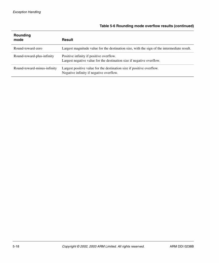
Exception Handling
Round-toward-zero Largest magnitude value for the destination size, with the sign of the intermediate result.
Round-toward-plus-infinity Positive infinity if positive overflow.Largest negative value for the destination size if negative overflow.
Round-toward-minus-infinity Largest positive value for the destination size if positive overflow.Negative infinity if negative overflow.
Table 5-6 Rounding mode overflow results (continued)
Roundingmode Result
5-18 Copyright © 2002, 2003 ARM Limited. All rights reserved. ARM DDI 0238B

Exception Handling
5.9 Underflow exception
Underflow is detected pessimistically when the VFP9-S coprocessor is in Full-compliance mode.
5.9.1 Exception enabled
Setting the UFE bit, FPSCR[11], enables underflow exceptions. The VFP9-S coprocessor detects most underflow conditions conclusively, but it detects some pessimistically. The initial computation of the result exponent might be below a threshold for the destination precision. In this case, the possibility of underflow due to massive cancellation exists, but cannot be known in the first Execute stage. The VFP9-S coprocessor bounces on such cases and uses the support code to determine the exceptional status of the operation. If there is an underflow, either catastrophic or to a subnormal result, the support code writes the computed result to the destination register and returns without setting the UFC flag, FPSCR[3]. If there is no underflow, regardless of any accuracy loss, the intermediate result is written to the destination register, UFC is set, and the user trap handler is called. Underflow is confirmed if the result of the operation after rounding is less in magnitude than the smallest normalized number in the destination format. If it is confirmed, the intermediate result defined by the IEEE 754 standard is written to the destination register, and the Underflow exception user trap handler is called. The support code sets or clears the IXC flag, FPSCR[4], as appropriate.
When the VFP9-S coprocessor detects a pessimistic case, the EX flag, FPEXC[31], and the UFC flag, FPEXC[3], are set. The UFC flag in the FPSCR register is not set by the hardware and must be set by the support code before calling the Underflow exception user trap handler. The source and destination registers for the instruction are valid in the VFP9-S register file. See section Arithmetic exceptions on page 5-23 for the conditions that cause an underflow bounce.
5.9.2 Exception disabled
Clearing the UFE bit, FPSCR[11], disables Underflow exceptions. When the FZ bit, FPSCR[24], is not set, the VFP9-S coprocessor bounces on potential underflow cases in the same fashion as described in Exception enabled. The correct result is written to the destination register, setting the appropriate exception flags.
When the FZ bit is set, the VFP9-S coprocessor makes the determination of underflow before rounding and flushes any result that underflows. It returns a positive zero to the destination register and sets the UFC flag, FPSCR[3], and the IXC flag, FPSCR[4].
ARM DDI 0238B Copyright © 2002, 2003 ARM Limited. All rights reserved. 5-19

Exception Handling
Note
The determination of an underflow condition is made before rounding rather than after. This means that the VFP9-S coprocessor might not return the minimum normal value when rounding would have produced the minimum normal value. Instead, it flushes to zero an intermediate value with the minimum exponent for the destination precision, a fraction of all ones, and a round increment. If the intermediate value was the minimum normal value before the underflow condition test is made, it is not flushed to zero.
5-20 Copyright © 2002, 2003 ARM Limited. All rights reserved. ARM DDI 0238B
Exception Handling
5.10 Inexact exception
The result of an arithmetic operation on two floating-point values can have more significant bits than the destination register can contain. When this happens, the result is rounded to a value that the destination register can hold and is said to be inexact.
The Inexact exception occurs whenever:
• a result is not equal to the computed result before rounding
• an untrapped Overflow exception occurs
• an untrapped Underflow exception occurs, and there is loss of accuracy.
Note
The Inexact exception occurs frequently in normal floating-point calculations and does not indicate a significant numerical error except in some specialized applications. Enabling the Inexact exception by setting the IXE bit, FPSCR[12], can significantly reduce the performance of the VFP9-S coprocessor.
The VFP9-S coprocessor handles the Inexact exception differently from the other floating-point exceptions. It has no mechanism for reporting inexact results to the software, but can handle the exception without software intervention as long as the IXE bit, FPSCR[12], is cleared, disabling Inexact exceptions.
5.10.1 Exception enabled
If the IXE bit, FPSCR[12], is set, all CDP instructions are bounced to the support code without any attempt to perform the calculation. The support code is then responsible for performing the calculation, determining if any exceptions have taken place, and handling them appropriately. If it detects an Inexact exception, it calls the vuser trap handler.
Note If an Overflow or Underflow exception is also detected, it takes priority over the Inexact exception.
5.10.2 Exception disabled
If the IXE bit, FPSCR[12], is not set, the VFP9-S coprocessor writes the result to the destination register and sets the IXC flag, FPSCR[4].
ARM DDI 0238B Copyright © 2002, 2003 ARM Limited. All rights reserved. 5-21

Exception Handling
5.11 Input exceptions
The VFP9-S hardware processes most input operands. However, the hardware is incapable of processing some operands and bounces to support code to process the instruction. The inputs that bounce are:
• NaN operands, when Default NaN mode is not enabled
• subnormal operands, when Flush-to-Zero mode is not enabled.
5-22 Copyright © 2002, 2003 ARM Limited. All rights reserved. ARM DDI 0238B
Exception Handling
5.12 Arithmetic exceptions
This section describes the conditions under which the VFP9-S coprocessor bounces an arithmetic instruction pessimistically. It is the task of the support code to determine the actual exception status of the instruction. The support code must return either the result and appropriate exception status bits, or the intermediate result and a call to the user trap handler.
The following sections describe the circumstances in which arithmetic exceptions occur:
• FADD/FSUB/FCMP/FCMPZ/FCMPE/FCMPEZ on page 5-24
• FMUL/FNMUL on page 5-26
• FMAC/FMSC/FNMAC/FNMSC on page 5-27
• FDIV on page 5-27
• FSQRT on page 5-28
• FCPY/FABS/FNEG on page 5-28
• FCVTDS/FCVTSD on page 5-29
• FUITO/FSITO on page 5-29
• FTOUI/FTOUIZ/FTOSI/FTOSIZ on page 5-29.
ARM DDI 0238B Copyright © 2002, 2003 ARM Limited. All rights reserved. 5-23

Exception Handling
5.12.1 FADD/FSUB/FCMP/FCMPZ/FCMPE/FCMPEZ
In an addition or subtraction, or in a compare, which is effectively a subtraction, the exponent is initially the larger of the two input exponents. For clarity, we define the operation as a Like-Signed Addition (LSA) or an Unlike-Signed Addition (USA). Table 5-7 specifies how this distinction is made. In the table, + indicates a positive operand, and – indicates a negative operand.
Because it is possible for an LSA operation to cause the exponent to be incremented if the significand overflows, overflow bounce ranges for an LSA are more pessimistic than they are for a USA. The LSA ranges are made slightly more pessimistic to incorporate FMAC instructions (see FMAC/FMSC/FNMAC/FNMSC on page 5-27).
Underflow bounce ranges for a USA are more pessimistic than they are for an LSA. This is to accommodate a massive cancellation in which the result exponent is smaller than the larger operand exponent by as much as the length of the significand. The overflow range for a USA is slightly pessimistic (it is set to the LSA overflow range) to reduce the number of logic terms. Table 5-8 on page 5-25 shows the USA and LSA values and conditions.
Table 5-7 LSA and USA determination
InstructionOperand Asign
Operand Bsign
Operationtype
FADD + + LSA
FADD + – USA
FADD – + USA
FADD – – LSA
FSUB/FCMP + + USA
FSUB/FCMP + – LSA
FSUB/FCMP – + LSA
FSUB/FCMP – – USA
5-24 Copyright © 2002, 2003 ARM Limited. All rights reserved. ARM DDI 0238B

Exception Handling
Table 5-8 FADD family bounce thresholds
Exponent value
Float value
Condition when not in Flush-to-Zero mode
D-Pa S-Pb S-P D-P
>0x7FF - D-P overflow - Bounce
0x7FF - D-P overflow, NaN, or infinity - Bounce
0x7FE - D-P overflow - Bounce
0x7FD - D-P overflow - Bounce
0x7FC - D-P normal - Normal
>0x47F >0xFF S-P overflow Bounce Normal
0x47F 0xFF S-P NaN or infinity Bounce Normal
0x47E 0xFE S-P overflow Bounce Normal
0x47D 0xFD S-P overflow Bounce Normal
0x47C 0xFC S-P normal Normal Normal
0x3FF 0x7F e = 0 bias value Normal Normal
0x3A0 0x20 S-P normal (LSA) Minimum (USA) Normal
0x39F 0x1F S-P underflow (USA) Bounce (USA) or normal (LSA) Normal
0x381 0x01 S-P normal (LSA) MIN (LSA) Normal
0x380 0x00 S-P subnormal Bounce Normal
<0x380 <0x00 S-P underflow Bounce Normal
0x040 - D-P normal (USA) - Normal (LSA) or minimum (USA)
0x03F - D-P underflow (USA) - Normal (LSA) or bounce (USA)
0x001 - D-P normal (LSA) - Minimum (LSA) or bounce (USA)
0x000 - D-P subnormal - Bounce
<0x000 - D-P underflow - Bounce
a. D-P = double-precision.b. S-P = single-precision.
ARM DDI 0238B Copyright © 2002, 2003 ARM Limited. All rights reserved. 5-25

Exception Handling
5.12.2 FMUL/FNMUL
Detection of a potential exception is based on the initial product exponent, which is the sum of the multiplicand and multiplier exponents. Table 5-9 shows the result for specific values of the initial product exponent. The exponent can be incremented by a significand overflow condition, which is the cause for the additional bounce values near the real overflow threshold. The one additional value in the bounce range makes the FMUL/FNMUL overflow detection ranges identical to those in Table 5-8 on page 5-25.
Table 5-9 FMUL family bounce thresholds
Exponent value
Float value
Condition in Full-compliance mode
D-Pa
a. D-P = double-precision.
S-Pb
b. S-P = single-precision.
S-P D-P
>0x7FF - D-P overflow - Bounce
0x7FF - D-P NaN or infinity - Bounce
0x7FE - D-P maximum normal - Bounce
0x7FD - D-P normal - Bounce
0x7FC - D-P normal - Normal
>0x47F >0xFF S-P overflow Bounce Normal
0x47F 0xFF S-P NaN or infinity Bounce Normal
0x47E 0xFE S-P maximum normal Bounce Normal
0x47D 0xFD S-P normal Bounce Normal
0x47C 0xFC S-P normal Normal Normal
0x3FF 0x7F e = 0 bias value Normal Normal
0x381 0x01 S-P normal Normal Normal
0x380 0x00 S-P subnormal Bounce Normal
<0x380 <0x00 S-P underflow Bounce Normal
0x001 - D-P normal - Normal
0x000 - D-P subnormal - Bounce
<0x000 - D-P underflow - Bounce
5-26 Copyright © 2002, 2003 ARM Limited. All rights reserved. ARM DDI 0238B

Exception Handling
5.12.3 FMAC/FMSC/FNMAC/FNMSC
The FMAC family of operations adds to the potential overflow range by generating significand values from zero up to but not including four. In this case it is possible for the final exponent to require incrementing by two to normalize the significand.
The bounce thresholds for the FADD family in Table 5-8 on page 5-25 and for the FMUL family in Table 5-9 on page 5-26 incorporate this additional factor. Those ranges are used to detect potential exceptions for the FMAC family.
5.12.4 FDIV
The thresholds for divide are simple and based only on the difference of the exponents of the dividend and the divisor. It is not possible in a divide operation for the significand to overflow and cause an increment of the exponent. However, it is possible for the significand to require a single bit left shift and the exponent to be decremented for normalization. To reduce logic complexity, the overflow ranges are the same as those of the LSA operations in FADD/FSUB/FCMP/FCMPZ/FCMPE/FCMPEZ on page 5-24. The underflow ranges include the minimum normal exponent, 0x01 for single-precision and 0x001 for double-precision. Table 5-10 shows the FDIV bounce thresholds.
Table 5-10 FDIV bounce thresholds
Exponent value
Float value
Condition in Full-compliance mode
D-Pa S-Pb S-P D-P
>0x7FF - D-P overflow - Bounce
0x7FF - D-P NaN or infinity - Bounce
0x7FE - D-P maximum normal - Bounce
0x7FD - D-P normal - Bounce
0x7FC - D-P normal - Normal
>0x47F >0xFF S-P overflow Bounce Normal
0x47F 0xFF S-P NaN or infinity Bounce Normal
0x47E 0xFE S-P maximum normal Bounce Normal
0x47D 0xFD S-P normal Bounce Normal
0x47C 0xFC S-P normal Normal Normal
ARM DDI 0238B Copyright © 2002, 2003 ARM Limited. All rights reserved. 5-27

Exception Handling
5.12.5 FSQRT
It is not possible for FSQRT to overflow or underflow.
5.12.6 FCPY/FABS/FNEG
It is not possible for FCPY, FABS, or FNEG to bounce for any operand.
0x3FF 0x7F e = 0 bias value Normal Normal
0x382 0x02 S-P normal Normal Normal
0x381 0x01 S-P normal Bounce Normal
0x380 0x00 S-P subnormal Bounce Normal
<0x380 <0x00 S-P underflow Bounce Normal
0x002 - D-P normal - Normal
0x001 - D-P normal - Bounce
0x000 - D-P subnormal - Bounce
<0x000 - D-P underflow - Bounce
a. D-P = double-precision.b. S-P = single-precision.
Table 5-10 FDIV bounce thresholds (continued)
Exponent value
Float value
Condition in Full-compliance mode
D-Pa S-Pb S-P D-P
5-28 Copyright © 2002, 2003 ARM Limited. All rights reserved. ARM DDI 0238B

Exception Handling
5.12.7 FCVTDS/FCVTSD
Only the FCVTSD operation is capable of overflow or underflow. To reduce logic complexity, the overflow ranges are the same as the LSA ranges. Table 5-11 lists the FCVTSD bounce conditions.
5.12.8 FUITO/FSITO
It is not possible to generate overflow or underflow in an integer-to-float conversion.
5.12.9 FTOUI/FTOUIZ/FTOSI/FTOSIZ
Float-to-integer conversions generate Invalid Operation exceptions rather than Overflow or Underflow exceptions. To support signed conversions with round-toward-zero rounding in the maximum range possible for C, C++, and Java compiled code, the thresholds for pessimistic bouncing are different for the various rounding modes.
Table 5-12 on page 5-31 and Table 5-13 on page 5-32 use the following notation:
In the VFP Response column, the response notations are:
all These input values are bounced for all rounding modes.
Table 5-11 FCVTSD bounce thresholds
Exponent value Float valueFCVTSD conditionin Full-compliance mode
>0x47F S-Pa overflow Bounce
0x47F S-P NaN or infinity Bounce
0x47E S-P maximum normal Bounce
0x47D S-P normal Bounce
0x47C S-P normal Normal
0x3FF e = 0 bias value Normal
0x381 S-P normal Normal
0x380 S-P subnormal Bounce
<0x380 S-P underflow Bounce
a. S-P = single-precision.
ARM DDI 0238B Copyright © 2002, 2003 ARM Limited. All rights reserved. 5-29
Exception Handling
S These input values are bounced for signed conversions in all rounding modes.
SnZ These input values are bounced for signed conversions in all rounding modes except round-toward-zero.
U These input values are bounced for unsigned conversions in all rounding modes.
UnZ These input values are bounced for unsigned conversions in all rounding modes except round-toward-zero.
In the Unsigned results and Signed results columns, the rounding mode notations are:
N Round-to-nearest mode.
P Round-toward-plus-infinity mode.
M Round-toward-minus infinity mode.
Z Round-toward-zero mode.
Table 5-12 on page 5-31 shows the single-precision float-to-integer bounce range and the results returned for exceptional conditions.
5-30 Copyright © 2002, 2003 ARM Limited. All rights reserved. ARM DDI 0238B

Exception Handling
Table 5-12 Single-precision float-to-integer bounce thresholds and stored results
Floating-pointvalue
Integervalue
Unsignedresult Status
Signedresult Status
VFP9-Sresponse
NaN - 0x00000000 Invalid 0x00000000 Invalid Bounce all
0x7F800000 +infinity 0xFFFFFFFF Invalid 0x7FFFFFFF Invalid Bounce all
0x7F7FFFFF to0x4F800000
+maximum S-Pa
to232
0xFFFFFFFF Invalid 0x7FFFFFFF Invalid Bounce all
0x4F7FFFFF
to0x4F000000
(232 - 28)to231
0xFFFFFF00
to0x80000000
Invalid 0x7FFFFFFF Invalid Bounce S UnZ
0x4EFFFFFF to0x4E800000
(231 - 27)to230
0x7FFFFF80
to0x40000000
- 0x7FFFFF80
to0x40000000
- Bounce SnZ
0x4E7FFFFF
to0x00000000
(230 - 26)to+0
0x3FFFFFC0
to0x00000000
- 0x3FFFFFC0
to0x00000000
- No bounce
0x80000000
to0xCE7FFFFF
–0to(–230 +26)
0x00000000 Invalidb 0x00000000
to0xC0000040
- Bounce U
0xCE800000
to0xCEFFFFFF
-230to(-231 +27)
0x00000000 Invalid 0xC0000000
to0x80000080
- Bounce U
Bounce U SnZ
0xCF000000
to0xFF7FFFFF
-231to–maximum S-P
0x00000000 Invalid 0x80000000 Invalid Bounce all
0xFF800000 –infinity 0x00000000 Invalid 0x80000000 Invalid Bounce all
a. S-P = single-precision.b. A negative input value that rounds to a zero result returns zero and is not invalid.
ARM DDI 0238B Copyright © 2002, 2003 ARM Limited. All rights reserved. 5-31
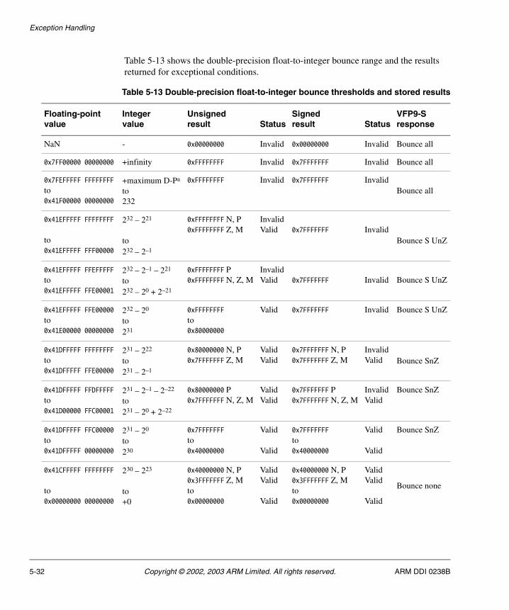
Exception Handling
Table 5-13 shows the double-precision float-to-integer bounce range and the results returned for exceptional conditions.
Table 5-13 Double-precision float-to-integer bounce thresholds and stored results
Floating-pointvalue
Integervalue
Unsignedresult Status
Signedresult Status
VFP9-Sresponse
NaN - 0x00000000 Invalid 0x00000000 Invalid Bounce all
0x7FF00000 00000000 +infinity 0xFFFFFFFF Invalid 0x7FFFFFFF Invalid Bounce all
0x7FEFFFFF FFFFFFFF to0x41F00000 00000000
+maximum D-Pa
to232
0xFFFFFFFF Invalid 0x7FFFFFFF InvalidBounce all
0x41EFFFFF FFFFFFFF
to0x41EFFFFF FFF00000
232 – 221
to232 – 2–1
0xFFFFFFFF N, P0xFFFFFFFF Z, M
InvalidValid 0x7FFFFFFF Invalid
Bounce S UnZ
0x41EFFFFF FFEFFFFF
to0x41EFFFFF FFE00001
232 – 2–1 – 221
to232 – 20 + 2–21
0xFFFFFFFF P0xFFFFFFFF N, Z, M
InvalidValid 0x7FFFFFFF Invalid Bounce S UnZ
0x41EFFFFF FFE00000
to0x41E00000 00000000
232 – 20
to231
0xFFFFFFFF
to0x80000000
Valid 0x7FFFFFFF Invalid Bounce S UnZ
0x41DFFFFF FFFFFFFF to 0x41DFFFFF FFE00000
231 – 222
to231 – 2–1
0x80000000 N, P0x7FFFFFFF Z, M
ValidValid
0x7FFFFFFF N, P0x7FFFFFFF Z, M
InvalidValid Bounce SnZ
0x41DFFFFF FFDFFFFF
to0x41D00000 FFC00001
231 – 2–1 – 2–22
to231 – 20 + 2–22
0x80000000 P0x7FFFFFFF N, Z, M
ValidValid
0x7FFFFFFF P0x7FFFFFFF N, Z, M
InvalidValid
Bounce SnZ
0x41DFFFFF FFC00000
to0x41DFFFFF 00000000
231 – 20
to230
0x7FFFFFFF
to0x40000000
Valid
Valid
0x7FFFFFFF
to0x40000000
Valid
Valid
Bounce SnZ
0x41CFFFFF FFFFFFFF
to0x00000000 00000000
230 – 223
to+0
0x40000000 N, P0x3FFFFFFF Z, Mto0x00000000
ValidValid
Valid
0x40000000 N, P0x3FFFFFFF Z, Mto0x00000000
ValidValid
Valid
Bounce none
5-32 Copyright © 2002, 2003 ARM Limited. All rights reserved. ARM DDI 0238B

Exception Handling
0x80000000 00000000
to0xC1CFFFFF FFFFFFFF
–0to–230 + 2–23)
0x00000000b Invalid 0x00000000
to0xC0000001 Z, P0xC0000000 N, M
Valid
ValidValid
Bounce U
0xC1D00000 00000000
to0xC1DFFFFF FFFFFFFF
–230
to–231 + 2–22
0x00000000 Invalid 0xC0000000
to0x80000001 Z, P0x80000000 N, M
Valid
InvalidInvalid
Bounce U SnZ
0xC1E00000 00000000 –2–31 0x00000000 Invalid 0x80000000 Valid Bounce all
0xC1E00000 00000001
to0xC1E00000 00100000
–2–31 – 2–21
to–2–31 – 2–1
0x00000000 Invalid 0x80000000 N, Z, P0x80000000 M
ValidInvalid
Bounce all
0xC1E00000 00100001
to0xC1E00000 001FFFFF
–2–31 – 2–1 – 2–21
to2–31 – 20
0x00000000 Invalid 0x80000000 Z, P0x80000000 N, M
Valid Bounce all
0xC1E00000 00200000
to0xFFEFFFFF FFFFFFFF
2–31 – 20 –2–21
to–maximum D-P
0x00000000 Invalid 0x80000000 Invalid Bounce all
0xFFF00000 00000000 –infinity 0x00000000 Invalid 0x00000000 Invalid Bounce all
a. D-P = double-precision.b. A negative input value that rounds to a zero result returns zero and is not invalid.
Table 5-13 Double-precision float-to-integer bounce thresholds and stored results (continued)
Floating-pointvalue
Integervalue
Unsignedresult Status
Signedresult Status
VFP9-Sresponse
ARM DDI 0238B Copyright © 2002, 2003 ARM Limited. All rights reserved. 5-33

Exception Handling
5-34 Copyright © 2002, 2003 ARM Limited. All rights reserved. ARM DDI 0238B

Chapter 6 Design for Test
This chapter describes the Design For Test (DFT) features of the VFP9-S coprocessor and describes how to integrate the DFT features into an SoC. This chapter contains the following sections:
• VFP9-S coprocessor on page 6-2
• VFP9-S test wrapper on page 6-3
• Test Pins on page 6-6.
ARM DDI 0238B Copyright © 2002, 2003 ARM Limited. All rights reserved. 6-1

Design for Test
6.1 VFP9-S coprocessor
Except for reset, the VFP9-S coprocessor is a synchronous, full-scan mux-D flip-flop design. It contains one internal clock domain controlled by the GCLK pin. It has 3 418 flip-flops, not counting the dedicated test wrapper cells. Including the dedicated test wrapper cells, there are 3 493 flip-flops.
6.1.1 Clock gating
Asserting DFTCKEN enables the clock. DFTCKEN must be asserted during functional mode and test mode. You can negate DFTCKEN to easily disable the clock when the VFP9-S coprocessor must hold its state. You can negate DFTCKEN to let the VFP9-S coprocessor stay in a low-power mode while other SoC testing continues.
6.1.2 Reset synchronizer
A dual flip-flop synchronizer delivers the asynchronous CPRST signal to the flip-flops. When a wrapper is present, the first flip-flop in the synchronizer is a shared wrapper cell. Otherwise it is part of an internal scan chain. For direct control of the reset signal to all asynchronously reset flip-flops, the SCANMODE signal blocks the output of the second flip-flop. See Figure 6-1.
Figure 6-1 Reset synchronizer
Note During scan mode, the 0 input of the multiplexor in Figure 6-1 is not tested.
Reset to flip-flops
SCANMODEGCLK
DFTRESET
CPRST
0
1
6-2 Copyright © 2002, 2003 ARM Limited. All rights reserved. ARM DDI 0238B
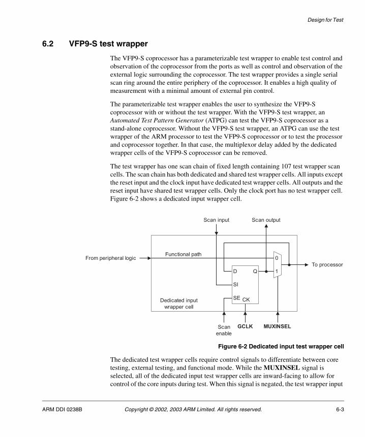
Design for Test
6.2 VFP9-S test wrapper
The VFP9-S coprocessor has a parameterizable test wrapper to enable test control and observation of the coprocessor from the ports as well as control and observation of the external logic surrounding the coprocessor. The test wrapper provides a single serial scan ring around the entire periphery of the coprocessor. It enables a high quality of measurement with a minimal amount of external pin control.
The parameterizable test wrapper enables the user to synthesize the VFP9-S coprocessor with or without the test wrapper. With the VFP9-S test wrapper, an Automated Test Pattern Generator (ATPG) can test the VFP9-S coprocessor as a stand-alone coprocessor. Without the VFP9-S test wrapper, an ATPG can use the test wrapper of the ARM processor to test the VFP9-S coprocessor or to test the processor and coprocessor together. In that case, the multiplexor delay added by the dedicated wrapper cells of the VFP9-S coprocessor can be removed.
The test wrapper has one scan chain of fixed length containing 107 test wrapper scan cells. The scan chain has both dedicated and shared test wrapper cells. All inputs except the reset input and the clock input have dedicated test wrapper cells. All outputs and the reset input have shared test wrapper cells. Only the clock port has no test wrapper cell. Figure 6-2 shows a dedicated input wrapper cell.
Figure 6-2 Dedicated input test wrapper cell
The dedicated test wrapper cells require control signals to differentiate between core testing, external testing, and functional mode. While the MUXINSEL signal is selected, all of the dedicated input test wrapper cells are inward-facing to allow for control of the core inputs during test. When this signal is negated, the test wrapper input
From peripheral logic
To processor
Scan input Scan output
Functional path
Scan
enable
GCLK MUXINSEL
Dedicated input
wrapper cell
D
SI
CK
Q
SE
0
1
ARM DDI 0238B Copyright © 2002, 2003 ARM Limited. All rights reserved. 6-3

Design for Test
cells can observe data from logic that is peripheral to the core. This is also the state for functional mode. All of the output ports use shared wrapper cells and do not need this type of control. Figure 6-3 shows a shared input and a shared output test wrapper cell.
Figure 6-3 Shared input and shared output test wrapper cells
6.2.1 WSEI and WSEO
The test wrapper contains two scan enable signals:
WSEI Wrapper scan enable input. WSEI connects only to the wrapper cells adjacent to the functional inputs.
WSEO Wrapper scan enable output. WSEO connects only to the wrapper cells adjacent to the functional outputs.
If your application does not require separate WSEI and WSEO signals, you can tie them together as one wrapper scan enable signal.
Peripheral logic To processor
Scan
input
Scan output
D
SDI
CLK
QFunctional input
Core input cell
GCLK
Scan output
Scan
input
D
SDI
CLK
QFunctional output
Core output cell
From processor
GCLK
Peripheral logic
6-4 Copyright © 2002, 2003 ARM Limited. All rights reserved. ARM DDI 0238B

Design for Test
6.2.2 WEDGE
The WEDGE signal enables you to select the clock edge on which the WSO port changes value. When WEDGE is HIGH, WSO changes on the next positive edge of the clock. When WEDGE is LOW, the signal goes through a lockup latch, and WSO changes on the next negative edge of the clock. WEDGE is useful when concatenating the wrapper chain with a scan chain in another clock domain.
Figure 6-4 Wrapper edge select logic
Last flip-flop in wrapper scan chain
WSO
WEDGE
GCLK
0
1
Lockup
latch
ARM DDI 0238B Copyright © 2002, 2003 ARM Limited. All rights reserved. 6-5
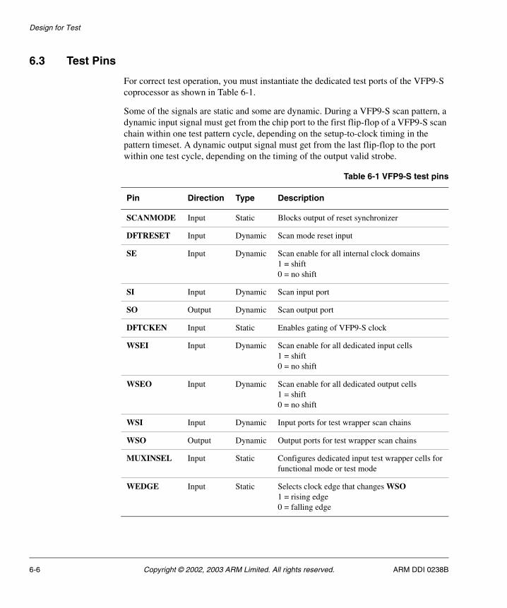
Design for Test
6.3 Test Pins
For correct test operation, you must instantiate the dedicated test ports of the VFP9-S coprocessor as shown in Table 6-1.
Some of the signals are static and some are dynamic. During a VFP9-S scan pattern, a dynamic input signal must get from the chip port to the first flip-flop of a VFP9-S scan chain within one test pattern cycle, depending on the setup-to-clock timing in the pattern timeset. A dynamic output signal must get from the last flip-flop to the port within one test cycle, depending on the timing of the output valid strobe.
Table 6-1 VFP9-S test pins
Pin Direction Type Description
SCANMODE Input Static Blocks output of reset synchronizer
DFTRESET Input Dynamic Scan mode reset input
SE Input Dynamic Scan enable for all internal clock domains1 = shift0 = no shift
SI Input Dynamic Scan input port
SO Output Dynamic Scan output port
DFTCKEN Input Static Enables gating of VFP9-S clock
WSEI Input Dynamic Scan enable for all dedicated input cells1 = shift0 = no shift
WSEO Input Dynamic Scan enable for all dedicated output cells1 = shift0 = no shift
WSI Input Dynamic Input ports for test wrapper scan chains
WSO Output Dynamic Output ports for test wrapper scan chains
MUXINSEL Input Static Configures dedicated input test wrapper cells forfunctional mode or test mode
WEDGE Input Static Selects clock edge that changes WSO1 = rising edge0 = falling edge
6-6 Copyright © 2002, 2003 ARM Limited. All rights reserved. ARM DDI 0238B

Design for Test
6.3.1 Test pin configuration in scan test with wrapper
Table 6-2 shows the configuration of the VFP9-S coprocessor test ports during core testing when the wrapper is available. All wrapper-only test signals are marked with an asterisk and are not a factor if the wrapper is not synthesized.
A test control module can be created to control the states of the static test signals.
6.3.2 Test pin configuration in functional mode
Table 6-3 on page 6-8 shows the configuration of the VFP9-S coprocessor test ports during functional mode. All wrapper-only test signals are marked with an asterisk and are not a factor if the wrapper is not synthesized.
Table 6-2 VFP9-S test pins during scan test
Pin Connection
SCANMODE 1
DFTRESET Connect to external pin
DFTCKEN 1
SE Connect to external pin
SI Connect to external pins
SO Connect to external pins
*WSEI Connect to external pin
*WSEO Connect to external pin
*MUXINSEL 1
*WSI Connect to external pins
*WSO Connect to external pins
*WEDGE User preference
ARM DDI 0238B Copyright © 2002, 2003 ARM Limited. All rights reserved. 6-7
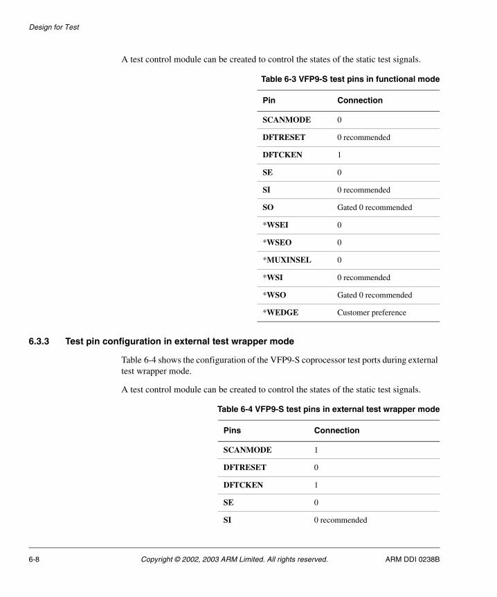
Design for Test
A test control module can be created to control the states of the static test signals.
6.3.3 Test pin configuration in external test wrapper mode
Table 6-4 shows the configuration of the VFP9-S coprocessor test ports during external test wrapper mode.
A test control module can be created to control the states of the static test signals.
Table 6-3 VFP9-S test pins in functional mode
Pin Connection
SCANMODE 0
DFTRESET 0 recommended
DFTCKEN 1
SE 0
SI 0 recommended
SO Gated 0 recommended
*WSEI 0
*WSEO 0
*MUXINSEL 0
*WSI 0 recommended
*WSO Gated 0 recommended
*WEDGE Customer preference
Table 6-4 VFP9-S test pins in external test wrapper mode
Pins Connection
SCANMODE 1
DFTRESET 0
DFTCKEN 1
SE 0
SI 0 recommended
6-8 Copyright © 2002, 2003 ARM Limited. All rights reserved. ARM DDI 0238B

Design for Test
SO Gated 0 recommended
WSEI Connected to pin
WSEO Connected to pin
MUXINSEL 0
WSI Connected to pin
WSO Connected to pin
WEDGE Connected to pin
Table 6-4 VFP9-S test pins in external test wrapper mode (continued)
Pins Connection
ARM DDI 0238B Copyright © 2002, 2003 ARM Limited. All rights reserved. 6-9

Design for Test
6-10 Copyright © 2002, 2003 ARM Limited. All rights reserved. ARM DDI 0238B
Chapter 7 Validating external connections
This chapter describes using the test wrapper to validate external connectivity between the VFP9-S coprocessor and the ARM9E processor. This chapter contains the following sections:
• About using the test wrapper on page 7-2
• Validation on page 7-3.
ARM DDI 0238B Copyright © 2002, 2003 ARM Limited. All rights reserved. 7-1

Validating external connections
7.1 About using the test wrapper
Each functional pin of the VFP9-S must be connected directly to the ARM9E processor. Both the ARM9E processor and the VFP9-S coprocessor can have a test wrapper to use with an ATPG tool to generate scan patterns for the manufacturing test of logic either inside or outside of the wrapper (see VFP9-S test wrapper on page 6-3)
Another use for the test wrapper is to validate the functional connections between the ARM9E processor and the VFP9-S coprocessor in the RTL. Because ATPG tools currently work only on gate level models, the validation patterns must be created manually.
7-2 Copyright © 2002, 2003 ARM Limited. All rights reserved. ARM DDI 0238B

Validating external connections
7.2 Validation
Table 7-1 on page 7-4 lists the functional VFP9-S input and output pins and where they are referenced in the VFP9-S test wrapper. The scan chain input is cell number 111 and the scan chain output is cell number 0. These 112 cells must be matched with the corresponding 112 cells in the test wrapper of the ARM9E processor. See the DFT chapter in the Technical Reference Manual of your ARM9E processor for details.
Each VFP9-S wrapper input cell must have a corresponding ARM wrapper output cell. Each ARM wrapper input cell must have a corresponding VFP9-S wrapper output. It is then possible to use the scan interface to:
• shift control values into the output cells of each chain
• perform a scan capture
• shift observe values out of the input cells of each chain.
The sequence of control and observe values chosen can then be used in simulation to validate the connectivity using this procedure:
1. Configure both chains for EXTEST operation (see Test pin configuration in external test wrapper mode on page 6-8).
2. For each of the output cells from both chains:
a. Shift a logic one into the selected output cell, and shift zeros into all other output cells of both chains. The values of the input cells have no effect.
b. Negate the scan enables that control the input cells of each chain (WSEI in the VFP9-S coprocessor) and capture into the input cells of each chain.
c. Shift out captured values and expect a one for the input cell that corresponds to the selected output cell of the other chain and expect zeros for all other input cells of each chain. Values captured on the output cells have no effect.
Carefully following this procedure produces a test patttern that ensures that no port is unconnected, stuck high, stuck low, or connected to the wrong signal. The scan control pins and the clock pin, which do not actually have wrapper cells, are tested when using the scan interface to shift and capture in the pattern.
ARM DDI 0238B Copyright © 2002, 2003 ARM Limited. All rights reserved. 7-3

Validating external connections
Table 7-1 VFP9 test wrapper cell order
Cell number Cell type VFP9-S pin
111 Input CPINSTR[31]
110 Input CPINSTR[30]
109 Input CPINSTR[29]
108 Input CPINSTR[28]
107 Input CPINSTR[27]
106 Input CPINSTR[26]
105 Input CPINSTR[25]
104 Input CPINSTR[24]
103 Input CPINSTR[23]
102 Input CPINSTR[22]
101 Input CPINSTR[21]
100 Input CPINSTR[20]
99 Input CPINSTR[19]
98 Input CPINSTR[18]
97 Input CPINSTR[17]
96 Input CPINSTR[16]
95 Input CPINSTR[15]
94 Input CPINSTR[14]
93 Input CPINSTR[13]
92 Input CPINSTR[12]
91 Input CPINSTR[11]
90 Input CPINSTR[10]
89 Input CPINSTR[9]
88 Input CPINSTR[8]
87 Input CPINSTR[7]
86 Input CPINSTR[6]
85 Input CPINSTR[5]
84 Input CPINSTR[4]
83 Input CPINSTR[3]
82 Input CPINSTR[2]
81 Input CPINSTR[1]
80 Input CPINSTR[0]
7-4 Copyright © 2002, 2003 ARM Limited. All rights reserved. ARM DDI 0238B
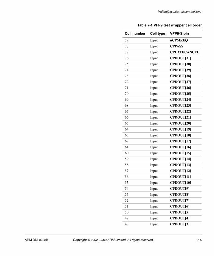
Validating external connections
79 Input nCPMREQ
78 Input CPPASS
77 Input CPLATECANCEL
76 Input CPDOUT[31]
75 Input CPDOUT[30]
74 Input CPDOUT[29]
73 Input CPDOUT[28]
72 Input CPDOUT[27]
71 Input CPDOUT[26]
70 Input CPDOUT[25]
69 Input CPDOUT[24]
68 Input CPDOUT[23]
67 Input CPDOUT[22]
66 Input CPDOUT[21]
65 Input CPDOUT[20]
64 Input CPDOUT[19]
63 Input CPDOUT[18]
62 Input CPDOUT[17]
61 Input CPDOUT[16]
60 Input CPDOUT[15]
59 Input CPDOUT[14]
58 Input CPDOUT[13]
57 Input CPDOUT[12]
56 Input CPDOUT[11]
55 Input CPDOUT[10]
54 Input CPDOUT[9]
53 Input CPDOUT[8]
52 Input CPDOUT[7]
51 Input CPDOUT[6]
50 Input CPDOUT[5]
49 Input CPDOUT[4]
48 Input CPDOUT[3]
Table 7-1 VFP9 test wrapper cell order
Cell number Cell type VFP9-S pin
ARM DDI 0238B Copyright © 2002, 2003 ARM Limited. All rights reserved. 7-5

Validating external connections
47 Input CPDOUT[2]
46 Input CPDOUT[1]
45 Input CPDOUT[0]
44 Input nCPTRANS
43 Input CPTBIT
42 Input CPCLKEN
41 Input CPBIGEND
40 Input CPRST
39 Output CHSDE[1]
38 Output CHSDE[0]
37 Output CHSEX[1]
36 Output CHSEX[0]
35 Output CPDIN[31]
34 Output CPDIN[30]
33 Output CPDIN[29]
32 Output CPDIN[28]
31 Output CPDIN[27]
30 Output CPDIN[26]
29 Output CPDIN[25]
28 Output CPDIN[24]
27 Output CPDIN[23]
26 Output CPDIN[22]
25 Output CPDIN[21]
24 Output CPDIN[20]
23 Output CPDIN[19]
22 Output CPDIN[18]
21 Output CPDIN[17]
20 Output CPDIN[16]
19 Output CPDIN[15]
18 Output CPDIN[14]
17 Output CPDIN[13]
16 Output CPDIN[12]
Table 7-1 VFP9 test wrapper cell order
Cell number Cell type VFP9-S pin
7-6 Copyright © 2002, 2003 ARM Limited. All rights reserved. ARM DDI 0238B

Validating external connections
15 Output CPDIN[11]
14 Output CPDIN[10]
13 Output CPDIN[9]
12 Output CPDIN[8]
11 Output CPDIN[7]
10 Output CPDIN[6]
9 Output CPDIN[5]
8 Output CPDIN[4]
7 Output CPDIN[3]
6 Output CPDIN[2]
5 Output CPDIN[1]
4 Output CPDIN[0]
3 Output CBURST[3]
2 Output CBURST[2]
1 Output CBURST[1]
0 Output CBURST[0]
Table 7-1 VFP9 test wrapper cell order
Cell number Cell type VFP9-S pin
ARM DDI 0238B Copyright © 2002, 2003 ARM Limited. All rights reserved. 7-7

Validating external connections
7-8 Copyright © 2002, 2003 ARM Limited. All rights reserved. ARM DDI 0238B
Glossary
This glossary defines some of the terms used in this manual.
Bounce When the VFP9-S coprocessor detects an illegal or architecturally UNDEFINED operation, it bounces the operation to the VFP support code. The VFP support code initiates exception processing through the UNDEFINED instruction trap. The VFP9-S coprocessor bounces an instruction by asserting CPBOUNCEE in the Decode stage of a trigger instruction.
See also Trigger instruction, Potentially exceptional instruction, and Exceptional state.
Coprocessor Data Processing (CDP) For the VFP9-S coprocessor, CDP operations are arithmetic operations rather than load or store operations.
Default NaN mode A mode enabled by setting the DN bit, FPSCR[25]. In this mode, all operations that result in a NaN return the default NaN, regardless of the cause of the NaN result. This mode is compliant with the IEEE 754 standard but implies that all information contained in any input NaNs to an operation is lost.
Denormalized value See Subnormal value.
ARM DDI 0238B Copyright © 2002, 2003 ARM Limited. All rights reserved. Glossary-1

Glossary
Disabled exception An exception is disabled when its exception enable bit in the FPCSR is not set. For these exceptions, the IEEE 754 standard defines the result to be returned. An operation that generates an exception condition can bounce to the support code to produce the result defined by the IEEE 754 standard. The exception is not reported to the user trap handler.
Enabled exception An exception is ensabled when its exception enable bit in the FPCSR is set. When an enabled exception occurs, a trap to the user handler is taken. An operation that generates an exception condition might bounce to the support code to produce the result defined by the IEEE 754 standard. The exception is then reported to the user trap handler.
Exceptional state When a potentially exceptional instruction is issued, the VFP9-S coprocessor sets the EX bit, FPEXC[31], and loads a copy of the potentially exceptional instruction in the FPINST register. If the instruction is a short vector operation, the register fields in FPINST are altered to point to the potentially exceptional iteration. When in the exceptional state, the issue of a trigger instruction to the VFP9-S coprocessor causes a bounce.
See also Bounce, Potentially exceptional instruction, and Trigger instruction.
Exponent The component of a floating-point number that normally signifies the integer power to which two is raised in determining the value of the represented number.
Fd The destination register and the accumulate value in triadic operations. Sd for single-precision operations and Dd for double-precision.
Fn The first source operand in dyadic or triadic operations. Sn for single-precision operations and Dn for double-precision.
Fm The second source operand in dyadic or triadic operations. Sm for single-precision operations and Dm for double-precision
Fraction The floating-point field that lies to the right of the implied binary point.
Flush-to-Zero mode A mode enabled by setting the FZ bit, FPSCR[24]. In this mode all inputs to arithmetic operations that are in the subnormal range for the input precision (–2Emin < x < 2Emin) and all results that are in the given range, before rounding, are treated as positive zero, rather than interpreted as, or converted to, a subnormal value.
IEEE 754 standard IEEE Standard for Binary Floating-Point Arithmetic, ANSI/IEEE Std 754-1985. The standard that defines data types, correct operation, exception types and handling, and error bounds for floating-point systems. Most processors are built in compliance with the standard in either hardware or a combination of hardware and software.
Illegal instruction An instruction that is architecturally UNDEFINED.
Infinity In the IEEE 754 standard format to represent infinity, the exponent is the maximum for the precision and the fraction is all zeros.
Glossary-2 Copyright © 2002, 2003 ARM Limited. All rights reserved. ARM DDI 0238B

Glossary
Input exception An exception condition in which one or more of the operands for a given operation are not supported by the hardware. The operation bounces to support code for processing.
Intermediate result An internal format used to store the result of a calculation before rounding. This format can have a larger exponent field and fraction field than the destination format.
MCR/MCRR A class of data transfer instructions that transfer 32-bit or 64-bit quantities from ARM registers to VFP9-S registers.
MRC/MRRC A class of data transfer instructions that transfer 32-bit or 64-bit quantities from VFP9-S registers to ARM registers.
NaN Not a number. A symbolic entity encoded in a floating-point format that has the maximum exponent field and a nonzero fraction. An SNaN causes an invalid operand exception if used as an operand and a most significant fraction bit of zero. A QNaN propagates through almost every arithmetic operation without signaling exceptions and has a most significant fraction bit of one.
Potentially exceptional instruction An instruction that is determined, based on the exponents of the operands and the sign bits, to have the potential to produce an overflow or underflow condition. Once this determination is made, the VFP enters the exceptional state and bounces the next trigger instruction issued.
See also Bounce, Trigger instruction, and Exceptional state.
Register banks Four banks of registers for both scalar and short vector floating-point operations. In single-precision operations, each bank contains eight single-precision registers. In double-precision operations, each bank contains four double-precision registers.
Reserved A field in a control register or instruction format is reserved if the field is to be defined by the implementation, or produces UNPREDICTABLE results if the field not cleared. These fields are reserved for use in future extensions of the architecture or are implementation-specific. All reserved bits not used by the implementation read as zero, and, when written, must be cleared.
Rounding mode The IEEE 754 standard requires all calculations to be performed as if to an infinite precision. For example, a multiply of two single-precision values must accurately calculate the significand to twice the number of bits of the significand. To represent this value in the destination precision, rounding of the significand is often required. The IEEE 754 standard specifies four rounding modes.
In round-to-nearest mode, the result is rounded at the halfway point, with the tie case rounding up if it would clear the least significant bit of the significand, making it even. Round-toward-zero mode chops any bits to the right of the significand, always rounding
ARM DDI 0238B Copyright © 2002, 2003 ARM Limited. All rights reserved. Glossary-3

Glossary
down, and is used by the C, C++, and Java languages in integer conversions. Round-toward-plus-infinity mode and round-to-minus-infinity mode are used in interval arithmetic.
RunFast mode In RunFast mode, hardware handles exceptional conditions and special operands. RunFast mode is enabled by enabling Default NaN and Flush-to-Zero modes and disabling all exceptions. In RunFast mode, the VFP9-S coprocessor does not bounce to the support code for any legal operation or any operand, but supplies a result to the destination. For all inexact and overflow results and all invalid operations that result from operations not involving NaNs, the result is as specified by the IEEE 754 standard. For operations involving NaNs, the result is the default NaN.
Scalar operation An operation involving a single source register and a single destination register.
Short vector operation
An operation involving more than one destination register and perhaps more than one source register in the generation of the result for each destination.
Significand The component of a binary floating-point number that consists of an explicit or implicit leading bit to the left of the implied binary point and a fraction field to the right.
Stride The stride field, FPSCR[21:20], specifies the increment applied to register addresses in short vector operations. A stride of 00, specifying an increment of +1, causes a short vector operation to increment each vector register by +1 for each iteration, while a stride of 11 specifies an increment of +2.
Subnormal value A representation of a value in the range (–2Emin < x < 2Emin). In the IEEE 754 standard format for single-precision and double-precision operands, a subnormal value has a zero exponent and a leading significant bit of zero. The IEEE 754 standard requires that the generation and manipulation of subnormal operands be performed with the same precision as normal operands.
Support code Software that must be used to complement the hardware to provide compatibility with the IEEE 754 standard. The support code must have a library of routines that performs supported functions, such as divide with unsupported inputs or inputs that might generate an exception as well as operations beyond the scope of the hardware. The support code must also have a set of exception handlers to process exceptional conditions in compliance with the IEEE 754 standard.
The support code is required to perform implemented functions to emulate proper handling of any unsupported data type or data representation. The routines can be written to use the VFP9-S coprocessor in their intermediate calculations if care is taken to restore the user state at the exit of the routine.
Trap An exceptional condition that has the respective exception enable bit set in the FPSCR register. The user provided trap handler is executed.
Glossary-4 Copyright © 2002, 2003 ARM Limited. All rights reserved. ARM DDI 0238B

Glossary
Trigger instruction The instruction that causes a bounce at the time it is issued. A potentially exceptional instruction causes the VFP9-S coprocessor to enter the exceptional state. The next instruction, unless it is an FMXR or FMRX instruction accessing the FPEXC, FPINST, or FPSID register, causes a bounce, beginning exception processing. The trigger instruction is not necessarily exceptional, and no processing of it is performed. It is retried at the return from exception processing of the potentially exceptional instruction.
See also Bounce, Potentially exceptional instruction, and Exceptional state.
UNDEFINED Indicates an instruction that generates an UNDEFINED instruction trap. See the ARM Architecture Reference Manual for more information on ARM exceptions.
UNPREDICTABLE The result of an instruction or control register field value that cannot be relied upon. UNPREDICTABLE instructions or results must not represent security holes, or halt or hang the processor, or any parts of the system.
Unsupported values Specific data values that are not processed by the hardware but bounced to the support code for completion. These data can include infinities, NaNs, subnormal values, and zeros. An implementation is free to select which of these values is supported in hardware fully or partially, or requires assistance from support code to complete the operation. Any exception resulting from processing unsupported data is trapped to user code if the corresponding exception enable bit for the exception is set.
ARM DDI 0238B Copyright © 2002, 2003 ARM Limited. All rights reserved. Glossary-5

Glossary
Glossary-6 Copyright © 2002, 2003 ARM Limited. All rights reserved. ARM DDI 0238B
Index
The items in this index are listed in alphabetical order, with symbols and numerics appearing at the end. The references given are to page numbers.
AArithmetic exception
support code 5-23Arithmetic exceptions 5-23–5-33ARM pipeline 4-4, 4-20, 4-21, 4-25
relation to VFP9-S pipeline 1-5ARM processor
executing conditional VFP code 1-18
memory formats 2-9–2-10test wrapper 6-3transferring data to and from VFP9-S
coprocessor 2-6–2-7Undefined Instruction exception
5-3using for float comparisons 1-18,
1-19, 3-6VFP9-S exception processing 5-2,
5-4VFP9-S interface 1-4
ARM processor clockrelation to VFP9-S clock 1-20
ARM v5TE instruction set 3-2
BBinary-to-decimal conversions 3-3Bounced instruction
Invalid Operation exception 5-14Overflow exception 5-17Underflow exception 5-19
Bounced instructionsarithmetic exceptions 5-23EX flag‚ FPEXC[31] 5-3, 5-6exception processing 5-2FADD family bounce thresholds
5-25FCVTSD bounce thresholds 5-29FDIV bounce thresholds 5-27float-to-integer conversion bounce
thresholds 5-31
Bounced instructions (continued)float-to-integer conversion
thresholds 5-32FMAC family bounce thresholds
5-27FMUL family bounce thresholds
5-26FPEXC register 3-21Full-compliance mode 4-8illegal instructions 5-6Inexact exception 5-21Input exception 5-22Input Subnormal exception 5-12overflow bounce ranges 5-24–5-33recursive 5-4RunFast mode 4-7scalar CDP instructions 5-8support code 5-3, 5-7tiny result 3-7trigger instruction 5-3Undefined Instruction exception
5-3UNDEFINED instructions 5-6, 5-8
ARM DDI 0238B Copyright © 2002, 2003 ARM Limited. All rights reserved. Index-1

Index
Bounced instructions (continued)underflow bounce ranges
5-24–5-33Underflow exception 5-19VFPv2 architecture 3-3without exception 5-3
Branch instructions 1-18
CC condition code flag‚ FPSCR[29]
description 3-18CHSDE[1:0] pins 7-6Circular register bank addressing 2-2,
2-11Comparison of single-precision and
double-precision values 3-3Condition code flags
CPSR[31:28] 3-6, 4-14FMSTAT example 4-14FPINST2[31:28] 3-23FPINST[31:28] 3-23FPSCR[31:28] 3-6, 4-3serializing instructions 4-3
Context switchpreventing data hazards 4-4saving and restoring registers 3-21
Control hazardparallel execution 4-23, 4-24RAR hazard 4-7
Conventionstypographical xiii
Coprocessor ID numbers 1-4CPBIGEND pin 7-6CPBURST[3:0] pins 7-7CPBURST[3:0] signals 1-16CPCLKEN pin 7-6CPDIN[31:0] pins 7-6CPDOUT[31:0] pins 7-5CPHSEX[1:0] pins 7-6CPINSTR[31:0] pins 7-4CPLATECANCEL pin 7-5CPPASS pin 7-5CPRST pin 6-2, 7-6CPTBIT pin 7-6
DData hazard 4-14–4-19
definition 4-7parallel execution 1-17, 4-23, 4-24preventing in context switch 4-4short vector instructions 1-15
Decimal-to-binary conversions 3-3Default NaN
Invalid Operation exception 5-14RunFast mode 1-13, 1-14
Default NaN mode 1-13comparisons 3-6enabling 1-12IEEE 754 standard compliance 3-2performance enhancement 3-4RunFast mode 1-13, 3-4
Destination registersshort vector instructions 1-15
DFTCKEN pin 6-2, 6-6external test wrapper mode 6-8functional mode 6-8scan test 6-7
DFTRESET pin 6-6external test wrapper mode 6-8functional mode 6-8scan test 6-7
Divide and square root (DS) pipeline 1-8
instructions 1-8latency 1-8, 4-20parallel operation 1-5, 1-17, 4-23,
4-24relation to ARM pipeline 1-5resource hazards 4-20short vector instructions 1-17throughput 1-5
Division-by-Zero exception 5-16enabling 5-16Flush-to-Zero mode 5-16Invalid Operation exception 5-16RunFast mode 1-14user trap handler 5-16
Division-by-zero operationRunFast mode 1-14
DN bit‚ FPSCR[25] 1-12description 3-18
Double-precision datacomparing with single-precision
data 3-3default NaN values 3-5exponent bias 2-4exponent bits 2-4format 2-3, 2-4, 2-8, 3-4fraction 2-4memory format 2-10minimum normal exponent 5-27NaNs 3-5numerical ranges 2-4register bank format 2-11sign bit 2-4SNG bit‚ FPSID[20] 3-17special formats 2-4transferring 2-6, 3-2
Double-precision instructionsabsolute value 5-11bounce thresholds of float-to-integer
conversions 5-32clearing source registers 4-12, 4-13coprocessor interface 1-4divide 1-8divide latency 4-20Fm, Fn, and Fd fields 2-5locking registers 4-9, 4-18locking source registers 4-11multiply 5-9multiply latency 4-20multiply-accumulate latency 4-20M, N, and D bits 2-5parallel execution 4-23square root 1-8square root latency 4-20three operand 2-15throughput 1-5, 1-9, 4-26two-operand 2-15VFP9-S support 1-2
DZC flag‚ FPSCR[1]description 3-19
DZC flag ƒPSCR[1]Division-by-Zero exception 5-16
DZE bit‚ FPSCR[9]description 3-18Division-by-Zero exception 5-16
Index-2 Copyright © 2002, 2003 ARM Limited. All rights reserved. ARM DDI 0238B

Index
EEN bit‚ FPEXC[30] 3-21
description 3-22Endian format 2-9EX flag‚ FPEXC[31] 3-21
bounced instructions 5-3description 3-22illegal instructions 5-6Input Subnormal exception 5-12preventing infinite exception loop
3-21, 5-4short vector exception processing
5-8Underflow exception 5-19
EX flag‚ FPSCR[31]Invalid Operation exception 5-14
Exception handler 5-3Exceptional state 3-21, 3-22, 5-2, 5-3Exceptions
Arithmetic exception 5-23arithmetic instructions 5-2copy instructions 5-2data transfer instructions 5-2Division-by-Zero exception 5-16IEEE 754 standard compliance 5-2,
5-4imprecise exception handling 5-7Inexact exception 5-21Input exception 5-22Input Subnormal exception 5-12Invalid Operation exception 5-13Overflow exception 5-17Undefined Instruction exception
5-7Underflow exception 5-19user trap handler 5-2
FFast interrupt (FIQ) mode 5-5Floating-point multiply and accumulate
(FMAC) pipeline 1-5, 1-7during short vector DS pipeline
operations 1-17, 1-19instructions 1-6parallel operation 1-5, 1-17, 4-23,
4-24
Floating-point multiply and accumulate (FMAC) pipeline (continued)
relation to ARM pipeline 1-5resource hazards 4-20throughput 1-5
Float-to-integer bounce rangedouble-precision 5-32single-precision 5-30
Float-to-integer conversionFull-compliance mode 1-13high-level language support 1-2Input Subnormal exception 5-12invalid condition 5-14Invalid Operation exception 5-14,
5-29Flush-to-Zero mode 3-2
comparisons 3-6Division-by-Zero exception 5-16enabling 1-12, 1-13IDC flag‚ FPSCR[7] 1-13, 3-2Input exception 5-22Input Subnormal exception 5-12IXC flag‚ FPSCR[4] 3-2, 5-19performance enhancement 3-4RunFast mode 1-13, 3-4subnormal input 1-13, 3-21tiny result 1-13, 3-7UFC flag‚ FPSCR[3] 1-13, 3-2, 3-7,
5-19underflow 3-2Underflow exception 5-19VFPv2 architecture 3-2
FMDRR instructioninteger data 3-10
FMRRD instructioninteger data 3-11
FMRRS instructioninteger data 3-14
FMSRR instructioninteger data 3-12
Forwardingfrom CDP instructions 4-5from integer-producing instructions
4-5from load instructions 4-5latency reduction 4-5, 4-26LS pipeline 1-9mixed-precision data 4-5, 4-6to store instructions 4-5, 4-6
FPEXC register 3-15accessing 3-16, 3-20, 4-3, 5-7bit fields 3-21bounced instructions 5-3changing context 3-21exception flags 3-21, 5-7exception processing example 5-9,
5-10, 5-11exception processing sequence 5-8FMXR,FMRX reg field code 3-16FP2V flag clearing example 5-9illegal instructions 5-6MCR instructions 2-6MRC instructions 2-6pessimistic detection of exceptions
3-21support code 3-21, 5-3, 5-4
FPINST register 3-15, 3-23, 5-3, 5-7accessing 3-16, 4-3, 5-7bounced instructions 5-3changing context 3-21condition code flags 3-23exception processing example 5-9,
5-10, 5-11FMXR, FMRX reg field code 3-16format 3-23MCR instructions 2-6MRC instructions 2-6reading by support code 5-4short vector exception 5-8
FPINST2 register 3-15, 3-23accessing 3-16, 4-3, 5-7changing context 3-21condition code flags 3-23exception processing example 5-9,
5-10, 5-11FMXR, FMRX reg field code 3-16format 3-23FP2V flag 5-4MCR instructions 2-6MRC instructions 2-6pretrigger slot 5-7pretrigger slot instruction 5-7support code 5-7
FPSCR exception flagsclearing 1-14IEEE 754 standard compliance 1-14
ARM DDI 0238B Copyright © 2002, 2003 ARM Limited. All rights reserved. Index-3
Index
FPSCR registeraccessing 3-16, 3-17, 4-3bit fields 3-17clearing IDC flag 3-2clearing UFC flag 3-2condition code flags 3-6, 4-3, 4-14FMXR, FMRX reg field code 3-16LEN field 2-2, 2-12, 3-19, 4-9,
4-11, 4-25MCR instructions 2-6MRC instructions 2-6reading by support code 5-4rounding mode 5-4STRIDE field 2-2, 3-19support code 1-13, 5-14, 5-19vector length 5-4writing by support code 5-4
FPSID register 3-15accessing 3-16, 3-17, 4-3, 5-7bit fields 3-16MCR instructions 2-6MRC instructions 2-6
FP2V flag‚ FPEXC[28]bounced instructions 5-4description 3-22exception processing example 5-9,
5-10, 5-11FSID register
FMXR,FMRX reg field code 3-16Full-compliance mode
exception processing 5-2IEEE 754 standard compliance
1-12, 3-4, 5-2interlocks 4-7Invalid Operation exception 5-13NaN processing 3-5overflow 1-12RAR hazards 1-19scoreboard operation 4-8support code 1-12underflow 1-12
FZ bit‚ FPSCR[24] 1-12description 3-18Input Subnormal exception 5-12performance enhancement 1-13Underflow exception 5-19
FZ bit‚ FPSCR[25]copying subnormal operand 5-2
GGCLK pin 6-2
HHazards
detection 4-7, 4-8Full-compliance mode 4-7RunFast mode 4-7see Control hazardsee Data hazardsee Read-after-read (RAR) hazardsee Read-after-write (RAW) hazardsee Resource hazardsee Write-after-read (WAR) hazardsee Write-after-write (WAW) hazard
IIDC flag‚ FPSCR[7]
description 3-18Flush-to-Zero mode 1-13, 3-2Input Subnormal exception 5-12VFPv2 architecture 3-2
IDE bit‚ FPSCR[15]description 3-18Input Subnormal exception 5-12VFPv2 architecture 3-2
IEEE 754 standard comparisons 3-7IEEE 754 standard compliance 1-2,
1-12, 3-3branch instructions 1-18, 1-19Default NaN mode 1-12, 3-2exceptions 3-8, 5-2, 5-4Flush-to-Zero mode 1-12Full-compliance mode 1-12, 3-4,
5-2Invalid Operation exception 5-14rounding modes 1-8RunFast mode 1-2, 1-12, 1-14, 3-4,
3-5, 5-2subnormal inputs 1-12Underflow exception 3-7, 5-19VFPv2 architecture 3-3VFP9-S instruction set 3-3
Imprecise exception handling 3-7, 5-7
Inexact exception 5-21enabling 5-21Full-compliance mode 1-12Overflow exception 5-21RunFast mode 1-14support code 5-21Underflow exception 5-21
Inexact operationRunFast mode 1-14
Input exception 3-21Flush-to-Zero mode 5-22NaN 3-21NaN input 5-22subnormal input 3-21, 5-22support code 5-22
Input Subnormal exceptionenabling 5-12float-to-integer conversion 5-12Flush-to-Zero mode 5-12support code 5-12VFPv2 architecture 3-2
Integer dataformat 2-3, 3-4forwarding 4-5
Integer instructionsFm, Fn, and Fd fields 2-5, 2-6M, N, and D bits 2-5
Integer-to-float conversionhigh-level language support 1-2overflow 5-29underflow 5-29
Integer-valued float 3-3Interlocks 4-7, 4-9INV flag‚ FPEXC[7] 3-21
description 3-22exception processing example 5-9,
5-10, 5-11Invalid operation
RunFast mode 1-14Invalid Operation exception 5-13–??
default NaN 5-14enabling 5-14example 5-9float-to-integer conversion 5-14Full-compliance mode 1-12, 1-13,
3-5, 5-13IEEE 754 standard compliance 5-14pessimistic detection 5-14QNaN compare with exception 3-6
Index-4 Copyright © 2002, 2003 ARM Limited. All rights reserved. ARM DDI 0238B

Index
Invalid Operation exception (continued)QNaN comparison 3-6RunFast mode 1-14, 5-13SNaN 2-3, 5-13SNaN compare with exception 3-6SNaN comparison 3-6SNaN input 3-5support code 5-13, 5-14transferring SNaNs 5-2user trap handler 5-14
Invalid operation exception ??–5-15IOC flag‚ FPEXC[0]
description 3-23exception processing example 5-9,
5-10, 5-11float-to-integer conversion 5-14Invalid Operation exception 5-14potential invalid operation 3-21
IOC flag‚ FPSCR[0] 5-14description 3-19Invalid Operation exception 5-14RunFast mode 3-5
IOE bit‚ FPSCR[8]description 3-18Full-compliance mode 1-12Invalid Operation exception 5-14setting IOC flag‚ FPEXC[0] 3-23SNaN comparison 3-6
IXC flag‚ FPSCR[4]description 3-19Flush-to-Zero mode 3-2, 5-19Inexact exception 5-21Overflow exception 5-17underflow 3-7Underflow exception 5-19VFPv2 architecture 3-2
IXE bit‚ FPSCR[12]bounced instructions 5-21description 3-18Full-compliance mode 1-12Inexact exception 5-21
LLEN field‚ FPSCR[18:16] 2-2, 4-25
description 3-19–3-20scalar instruction in short vector
mode 2-14
LEN field‚ FPSCR[18:16] (continued)scalar-only instruction 2-12short vector instruction with scalar
source 2-13short vector-only instruction 2-13
Load and store (LS) pipeline 1-5, 1-9, 1-10
instructions 1-10load data bus 1-9parallel operation 1-5, 1-17, 4-23,
4-24relation to ARM pipeline 1-5, 1-9resource hazards 4-20store data bus 1-9throughput 1-5
MMatrix operations 2-11Memory formats
big-endian 2-9, 2-10little-endian 2-9, 2-10
Mixed-precision data 4-5, 4-6Mixed-precision instructions 1-4MUXINSEL pin 6-3, 6-6
external test wrapper mode 6-9functional mode 6-8scan test 6-7
NN condition code flag‚ FPSCR[31]
description 3-18NaN
copy instructions 5-2data tranfer instructions 3-5default NaN values 3-5nonarithmetic CDP instructions 3-5see QNaN 2-3see SNaN 2-3support code 3-5valid 3-5
NaN inputFull-compliance mode 1-12RunFast mode 1-13, 1-14, 3-4
NaN resultRunFast mode 1-13
nCPMREQ pin 7-5nCPTRANS pin 7-6
OOFC flag‚ FPEXC[2]
description 3-23exception processing example 5-9,
5-10, 5-11potential overflow 3-21
OFC flag‚ FPSCR[2]description 3-19Overflow exception 5-17
OFE bit‚ FPSCR[10]description 3-18Full-compliance mode 1-12Overflow exception 5-17setting OFC flag‚ FPEXC[2] 3-23
OverflowFull-compliance mode 1-12negative 5-18positive 5-18potential 3-23rounding 5-17round-to-nearest mode 5-17round-toward-minus-infinity mode
5-17round-toward-plus-infinity mode
5-17round-toward-zero mode 5-17significand 5-17, 5-24
Overflow bounce ranges 5-24–5-33Overflow exception 5-17
enabling 5-17example 5-11Full-compliance mode 1-12Inexact exception 5-21pessimistic detection 5-17RunFast mode 1-14support code 5-17user trap handler 5-17
Overflow operationRunFast mode 1-14
ARM DDI 0238B Copyright © 2002, 2003 ARM Limited. All rights reserved. Index-5
Index
PPessimistic detection of exceptions
3-21, 5-3Arithmetic exception 5-23Invalid Operation exception 5-14Overflow exception 5-17Underflow exception 5-19
Pipelineparallel operation 1-5see Divide and square root (DS)
pipelinesee Floating-point multiply and
accumulate (FMAC) pipelinesee Load and store (LS) pipeline
Pretrigger slot 5-7Product revision status xii
QQNaN
compare with exception 3-6comparison 3-6definition 3-5Invalid Operation exception 3-5
RRAR hazard
see Read-after-read hazardRAW hazard
see Read-after-write hazardRead-after-read (RAR) hazard 4-8
definition 4-7example 4-17, 4-18
Read-after-write (RAW) hazard 1-19, 4-8
definition 4-7example 4-14, 4-15, 4-16
Remainder 3-3Remainder operation 3-3Resource hazard 4-7, 4-20
conditions 4-19example 4-21, 4-22parallel execution 4-24
Revisionstatus xii
Rmode field‚ FPSCR[23:22]description 3-18
Rounding float to integer-valued float 3-3
Rounding mode 5-4Round-toward-zero mode 1-2RunFast mode 1-14
bounce conditions 4-7Default NaN mode 3-4definition 1-13, 3-4division-by-zero operation 1-14exception processing 5-2Flush-to-Zero mode 3-4IEEE 754 standard compliance 1-2,
1-12, 1-14, 3-4, 3-5, 5-2inexact operation 1-14interlocks 4-7invalid operation 1-14Invalid Operation exception 5-13IOC bit‚ FPEXC[0] 3-23NaN processing 3-5OFC bit‚ FPEXC[2] 3-23overflow operation 1-14performance enhancement 3-4scoreboard operation 4-8
SScalar instruction
vector length 2-12, 2-14Scan chain 6-2, 6-3, 6-5SCANMODE pin 6-2, 6-6
external test wrapper mode 6-8functional mode 6-8scan test 6-7
Scoreboard 4-8lock mask 4-8lock register 4-8RunFast mode 4-8source and destination register
locking 4-8SE pin 6-6
external test wrapper mode 6-8functional mode 6-8scan test 6-7
Short vector instructions 2-13, 4-20circular register bank addressing
2-2, 2-11circular register banks 4-2clearing registers 4-8, 4-9crossing register bank boundary
2-11data hazard 1-15divide instructions 1-19divide iterations 4-4double-precision vector length 1-15DS pipeline 1-17exception processing 3-23, 5-4, 5-8,
5-10, 5-11exceptional iterations 4-14interlocks 4-9interrupt processing 4-4latency 4-4, 4-20locking registers 4-8, 4-9, 4-18mixing with scalar instructions 2-14number of operations 2-2parallel execution 1-17, 4-2, 4-23programming guidelines 1-19register bank addressing 2-2single-precision vector length 1-15square root 4-4square root instructions 1-19UNDEFINED 5-6UNPREDICTABLE 5-6vector length 2-13, 3-19, 3-20vector stride 2-13, 2-14, 3-19, 3-20
SI pin 6-6external test wrapper mode 6-8functional mode 6-8scan test 6-7
Signal processing operations 2-11Signaling NaN
see SNaN 2-3Single-precision data
comparing with double-precision data 3-3
default NaN values 3-5exponent bias 2-4exponent bits 2-4format 2-3, 2-8, 3-4fraction 2-4memory format 2-9minimum normal exponent 5-27NaNs 3-5, 3-7
Index-6 Copyright © 2002, 2003 ARM Limited. All rights reserved. ARM DDI 0238B

Index
Single-precision data (continued)numerical ranges 2-4register bank format 2-11sign bit 2-4SNG bit‚ FPSID[20] 3-17special formats 2-4transfering 3-2transfering to ARM processor 2-6
Single-precision instructionsadd 5-10bounce thresholds of float-to-integer
conversions 5-30clearing registers 4-9coprocessor interface 1-4divide 1-8divide latency 4-20Double-precision instructions
DS pipeline latency 1-8Fm, Fn, and Fd fields 2-5locking registers 4-9, 4-18locking source registers 4-9, 4-10multiply 5-10multiply-accumulate 5-11M, N, and D bits 2-5square root 1-8square root latency 4-20three operand 2-14throughput 1-5, 1-9, 4-26two-operand 2-15VFP9-S support 1-2
SNaNcompare with exception 3-6comparison 3-6data transfer instructions 5-2definition 3-5Invalid Operation exception 3-5,
5-13register access detection 2-3RunFast mode 3-5support code 5-13
SO pin 6-6external test wrapper mode 6-9functional mode 6-8scan test 6-7
Source registersshort vector instructions 1-15
STRIDE field‚ FPSCR[21:20] 2-2description 3-19–3-20scalar instruction in short vector
mode 2-14short vector instruction with scalar
source 2-13short vector-only instructions 2-13
Subnormal inputFlush-to-Zero mode 1-13, 3-21IDC flag‚ FPSCR[7] 3-2RunFast mode 1-14, 3-4
Subnormal operandcopying 5-2
Superscalar performance 4-2Support code 3-3, 5-3
Arithmetic exception 5-23clearing EX flag‚ FPEXC[31] 3-21computing intermediate result 5-4decoding FPINST instruction 5-4exception handlers 5-3exception handling 3-7executing FPINST2 instruction 5-4floating-point function library 5-3FPEXC register 3-15, 3-21FPINST register 3-15FPINST2 register 3-15, 3-23, 5-7FPSCR register 1-13Full-compliance mode 1-12, 3-4,
3-5IEEE 754 standard compliance 1-2,
1-13, 3-3, 3-4, 5-2illegal instructions 5-6Inexact exception 5-21infrequently occurring values 3-4Input exception 5-22Input Subnormal exception 5-12Invalid Operation exception 5-13,
5-14IXC flag‚ FPSCR[4] 5-17, 5-19library functions 3-3NaN processing 3-5Overflow exception 5-17overflow processing 3-8pretrigger slot instruction 5-7preventing infinite exception loops
5-4processing exceptions 5-4, 5-6reading FPEXC register 5-3reading FPINST register 5-4
Support code (continued)RunFast mode 1-2, 1-13, 1-14, 3-4,
3-5setting FPSCR register flags 5-4SNaN 5-13source data registers 3-15subnormal input 1-12tininess 3-7Underflow exception 5-19underflow processing 3-7, 3-8user trap handler 1-13using VFP9-S hardware for
calculations 5-4writing FPEXC register 5-4
System trap handler 3-21UNDEFINED trap handler 3-2
TTest wrapper
dedicated wrapper cell 6-2, 6-3shared wrapper cell 6-2, 6-3, 6-4validation 7-2–7-7
Tiny resultFlush-to-Zero mode 3-7RunFast mode 1-14
tiny resultFlush-to-Zero mode 1-13
Trigger instruction 3-7, 5-3, 5-8determination 5-7retrying 5-4
Typographical conventions xiii
UUFC flag‚ FPEXC[3]
description 3-22exception processing example 5-9,
5-10, 5-11potential underflow 3-21Underflow exception 5-19
UFC flag‚ FPSCR[2]description 3-19
UFC flag‚ FPSCR[3]Flush-to-Zero mode 1-13, 3-2, 3-7,
5-19Underflow exception 5-19
ARM DDI 0238B Copyright © 2002, 2003 ARM Limited. All rights reserved. Index-7
Index
UFE bit‚ FPSCR[11] 3-2description 3-18Flush-to-Zero mode 3-2Underflow exception 5-19
Undefined Instruction exception 5-3, 5-7
UNDEFINED trap handlersubnormal input 3-2underflow 3-2
UnderflowFlush-to-Zero mode 3-2Full-compliance mode 1-12potential 3-22RunFast mode 3-4
Underflow bounce ranges 5-24–5-33Underflow exception 5-19–5-20
enabling 5-19example 5-8Flush-to-Zero mode 5-19IEEE 754 standard compliance 3-7,
5-19Inexact exception 5-21IXC flag‚ FPSCR[4] 3-7pessimistic detection 5-19rounding 5-20support code 5-19UFC flag‚ FPSCR[3] 3-7user trap handler 5-19VFPv2 architecture 3-2
User trap handler 3-8, 3-21, 5-2Arithmetic exception 5-23bounced instruction 5-4Full-compliance mode 1-13Invalid Operation exception 3-5,
3-6, 5-14RunFast mode 3-4
VV condition code flag‚ FPSCR[28]
3-18VECITR field‚ FPEXC[10:8]
description 3-22exception processing example 5-9,
5-10, 5-11short vector exception processing
5-8Vector length 3-19, 4-3, 4-9, 4-18, 5-4
Vector stride 3-19VFPv2 architecture 1-2
compared to VFPv1 3-2Flush-to-Zero mode 3-2FPSID register encoding 3-17IDC flag‚ FPSCR[7] 3-2IDE bit‚ FPSCR[15] 3-2IEEE 754 standard compliance 3-3Input Subnormal exception 3-2instructions 3-3internal data format 2-3programmer’s model 3-2short vector operations 1-15, 2-13,
2-14UFC flag‚ FPSCR[3] 3-2Underflow exception 3-2
VFP9-S instruction setIEEE 754 standard compliance 3-3
VFP9-S pipelineinterlocks 4-7, 4-9interrupts 4-4parallel operation 4-24see Divide and square root pipelinesee Floating-point multiply and
accumulate pipelinesee Load and store pipelineserializing instructions 4-3source and destination register
determination 4-8VFP9-S pipeline hazards
see Read-after read (RAR) hazardsee Read-after-write (RAW) hazardsee Resource hazardsee Write-after-read (WAR) hazardsee Write-after-write (WAW) hazard
WWAR hazard
see Write-after-read hazardWAW hazard
see Write-after-write hazardWEDGE pin 6-5, 6-6
external test wrapper mode 6-9functional mode 6-8scan test 6-7
Write-after-read (WAR) hazard 4-8definition 4-7example 4-17, 4-19
Write-after-write (WAW) hazarddefinition 4-7
WSEI pin 6-4, 6-6, 7-3external test wrapper mode 6-9functional mode 6-8scan test 6-7
WSEO pin 6-4, 6-6external test wrapper mode 6-9functional mode 6-8scan test 6-7
WSI pin 6-6external test wrapper mode 6-9functional mode 6-8scan test 6-7
WSO pin 6-5, 6-6external test wrapper mode 6-9functional mode 6-8scan test 6-7
ZZ condition code flag‚ FPSCR[30]
branching 3-6description 3-18
Index-8 Copyright © 2002, 2003 ARM Limited. All rights reserved. ARM DDI 0238B