Embed Size (px)
Citation preview

VFP11™ Vector Floating-pointCoprocessor
for ARM1136JF-S processor r1p5
Technical Reference Manual
Copyright © 2002, 2003, 2005-2007 ARM Limited. All rights reserved.ARM DDI 0274H

VFP11 Vector Floating-point CoprocessorTechnical Reference Manual
Copyright © 2002, 2003, 2005-2007 ARM Limited. All rights reserved.
Release Information
The following changes have been made to this book.
Proprietary Notice
Words and logos marked with ® or ™ are registered trademarks or trademarks of ARM Limited in the EU and other countries, except as otherwise stated below in this proprietary notice. Other brands and names mentioned herein may be the trademarks of their respective owners.
Neither the whole nor any part of the information contained in, or the product described in, this document may be adapted or reproduced in any material form except with the prior written permission of the copyright holder.
The product described in this document is subject to continuous developments and improvements. All particulars of the product and its use contained in this document are given by ARM Limited in good faith. However, all warranties implied or expressed, including but not limited to implied warranties of merchantability, or fitness for purpose, are excluded.
This document is intended only to assist the reader in the use of the product. ARM Limited shall not be liable for any loss or damage arising from the use of any information in this document, or any error or omission in such information, or any incorrect use of the product.
Some material in this document is based on IEEE Standard for Binary Floating-Point Arithmetic, ANSI/IEEE Std 754-1985. The IEEE disclaims any responsibility or liability resulting from the placement and use in the described manner.
Change History
Date Issue Confidentiality Change
19 December 2002 A Non-Confidential First release
10 February 2003 B Non-Confidential First release for VFP11 r0p1 coprocessor
9 July 2003 C Non-Confidential First release for VFP11 r0p2 coprocessor
2 December 2003 D Non-Confidential FPINST2 reset state changed to Unpredictable
11 March 2005 E Non-Confidential First release for ARM1136JF-S r1p0 processor.
20 July 2005 F Non-Confidential First release for ARM1136JF-S r1p1 processor. Table 5-8 corrected.
06 December 2006 G Non-Confidential First release for r1p3. No change to functionality.
06 July 2007 H Non-Confidential First release for r1p5. No change to functionality.
ii Copyright © 2002, 2003, 2005-2007 ARM Limited. All rights reserved. ARM DDI 0274H
Confidentiality Status
This document is Non-Confidential. The right to use, copy and disclose this document may be subject to license restrictions in accordance with the terms of the agreement entered into by ARM and the party that ARM delivered this document to.
Product Status
The information in this document is final, that is for a developed product.
Web Address
http://www.arm.com
ARM DDI 0274H Copyright © 2002, 2003, 2005-2007 ARM Limited. All rights reserved. iii

iv Copyright © 2002, 2003, 2005-2007 ARM Limited. All rights reserved. ARM DDI 0274H

ContentsVFP11 Vector Floating-point Coprocessor Technical Reference Manual
PrefaceAbout this document ..................................................................................... xiiFeedback ...................................................................................................... xv
Chapter 1 Introduction1.1 About the VFP11 coprocessor .................................................................... 1-21.2 Applications ................................................................................................. 1-31.3 Coprocessor interface ................................................................................. 1-41.4 VFP11 coprocessor pipelines ..................................................................... 1-51.5 Modes of operation ................................................................................... 1-131.6 Short vector instructions ........................................................................... 1-161.7 Parallel execution of instructions ............................................................... 1-171.8 VFP11 treatment of branch instructions .................................................... 1-181.9 Writing optimal VFP11 code ...................................................................... 1-191.10 Product revisions ...................................................................................... 1-20
Chapter 2 Register File2.1 About the register file .................................................................................. 2-22.2 Register file internal formats ....................................................................... 2-32.3 Decoding the register file ............................................................................ 2-5
ARM DDI 0274H Copyright © 2002, 2003, 2005-2007 ARM Limited. All rights reserved. v

Contents
2.4 Loading operands from ARM1136JF-S registers ....................................... 2-62.5 Maintaining consistency in register precision ............................................. 2-82.6 Data transfer between memory and VFP11 registers ................................ 2-92.7 Access to register banks in CDP operations ............................................ 2-11
Chapter 3 Programmer’s Model3.1 About the programmer’s model .................................................................. 3-23.2 Compliance with the IEEE 754 standard .................................................... 3-33.3 ARMv5TE coprocessor extensions ............................................................ 3-93.4 VFP11 system registers ........................................................................... 3-15
Chapter 4 Instruction Execution4.1 About instruction execution ........................................................................ 4-24.2 Serializing instructions ................................................................................ 4-34.3 Interrupting the VFP11 coprocessor ........................................................... 4-44.4 Forwarding .................................................................................................. 4-54.5 Hazards ...................................................................................................... 4-74.6 Operation of the scoreboards ..................................................................... 4-84.7 Data hazards in full-compliance mode ..................................................... 4-154.8 Data hazards in RunFast mode ................................................................ 4-194.9 Resource hazards .................................................................................... 4-204.10 Parallel execution ..................................................................................... 4-244.11 Execution timing ....................................................................................... 4-26
Chapter 5 Exception Handling5.1 About exception processing ....................................................................... 5-25.2 Bounced instructions .................................................................................. 5-35.3 Support code .............................................................................................. 5-55.4 Exception processing ................................................................................. 5-85.5 Input Subnormal exception ....................................................................... 5-145.6 Invalid Operation exception ...................................................................... 5-155.7 Division by Zero exception ....................................................................... 5-185.8 Overflow exception ................................................................................... 5-195.9 Underflow exception ................................................................................. 5-215.10 Inexact exception ...................................................................................... 5-235.11 Input exceptions ....................................................................................... 5-245.12 Arithmetic exceptions ............................................................................... 5-25
Glossary
vi Copyright © 2002, 2003, 2005-2007 ARM Limited. All rights reserved. ARM DDI 0274H

List of TablesVFP11 Vector Floating-point Coprocessor Technical Reference Manual
Change History ............................................................................................................. iiTable 2-1 VFP11 MCR instructions ........................................................................................... 2-6Table 2-2 VFP11 MRC instructions ........................................................................................... 2-6Table 2-3 VFP11 MCRR instructions ........................................................................................ 2-7Table 2-4 VFP11 MRRC instructions ........................................................................................ 2-7Table 2-5 Single-precision data memory images and byte addresses ...................................... 2-9Table 2-6 Double-precision data memory images and byte addresses .................................... 2-9Table 2-7 Single-precision three-operand register usage ....................................................... 2-15Table 2-8 Single-precision two-operand register usage .......................................................... 2-15Table 2-9 Double-precision three-operand register usage ...................................................... 2-15Table 2-10 Double-precision two-operand register usage ........................................................ 2-16Table 3-1 Default NaN values ................................................................................................... 3-5Table 3-2 QNaN and SNaN handling ........................................................................................ 3-6Table 3-3 VFP11 system registers .......................................................................................... 3-15Table 3-4 Accessing VFP11 system registers ......................................................................... 3-16Table 3-5 FPSID Register bit fields ......................................................................................... 3-17Table 3-6 FPSCR Register bit fields ....................................................................................... 3-18Table 3-7 Vector length and stride combinations .................................................................... 3-20Table 3-8 FPEXC Register bit fields ........................................................................................ 3-22Table 3-9 Media and VFP Feature Register 0 bit fields .......................................................... 3-25Table 3-10 Media and VFP Feature Register 1 bit fields .......................................................... 3-26
ARM DDI 0274H Copyright © 2002, 2003, 2005-2007 ARM Limited. All rights reserved. vii

List of Tables
Table 4-1 Single-precision source register locking ................................................................... 4-9Table 4-2 Single-precision source register clearing ................................................................ 4-10Table 4-3 Double-precision source register locking ................................................................ 4-11Table 4-4 Double-precision source register clearing for one-cycle instructions ...................... 4-12Table 4-5 Double-precision source register clearing for two-cycle instructions ...................... 4-13Table 4-6 FCMPS-FMSTAT RAW hazard .............................................................................. 4-15Table 4-7 FLDM-FADDS RAW hazard ................................................................................... 4-16Table 4-8 FLDM-short vector FADDS RAW hazard ............................................................... 4-17Table 4-9 FMULS-FADDS RAW hazard ................................................................................. 4-17Table 4-10 Short vector FMULS-FLDMS WAR hazard ............................................................ 4-18Table 4-11 Short vector FMULS-FLDMS WAR hazard in RunFast mode ................................ 4-19Table 4-12 FLDM-FLDS-FADDS resource hazard ................................................................... 4-21Table 4-13 FLDM-short vector FMULS resource hazard .......................................................... 4-22Table 4-14 Short vector FDIVS-FADDS resource hazard, cycles 1 to 22 ................................ 4-22Table 4-15 Short vector FDIVS-FADDS resource hazard, cycles 23 to 36 .............................. 4-23Table 4-16 Parallel execution in all three pipelines ................................................................... 4-25Table 4-17 Throughput and latency cycle counts for VFP11 instructions ................................. 4-26Table 5-1 Exceptional short vector FMULD followed by load/store instructions ..................... 5-10Table 5-2 Exceptional short vector FADDS with a FADDS in the pretrigger slot .................... 5-12Table 5-3 Exceptional short vector FADDD with an FMACS trigger instruction ..................... 5-13Table 5-4 Possible Invalid Operation exceptions .................................................................... 5-15Table 5-5 Default results for invalid conversion inputs ........................................................... 5-17Table 5-6 Rounding mode overflow results ............................................................................ 5-20Table 5-7 LSA and USA determination ................................................................................... 5-25Table 5-8 FADD family bounce thresholds ............................................................................. 5-26Table 5-9 FMUL family bounce thresholds ............................................................................. 5-28Table 5-10 FDIV bounce thresholds ......................................................................................... 5-29Table 5-11 FCVTSD bounce thresholds ................................................................................... 5-31Table 5-12 Single-precision float-to-integer bounce thresholds and stored results .................. 5-32Table 5-13 Double-precision float-to-integer bounce thresholds and stored results ................. 5-33
viii Copyright © 2002, 2003, 2005-2007 ARM Limited. All rights reserved. ARM DDI 0274H

List of FiguresVFP11 Vector Floating-point Coprocessor Technical Reference Manual
Figure 1-1 FMAC pipeline ........................................................................................................... 1-6Figure 1-2 DS pipeline ................................................................................................................ 1-9Figure 1-3 LS pipeline .............................................................................................................. 1-10Figure 2-1 Single-precision data format ..................................................................................... 2-3Figure 2-2 Double-precision data format .................................................................................... 2-4Figure 2-3 Register file access ................................................................................................... 2-5Figure 2-4 Register banks ........................................................................................................ 2-11Figure 3-1 FMDRR instruction format ......................................................................................... 3-9Figure 3-2 FMRRD instruction format ....................................................................................... 3-10Figure 3-3 FMSRR instruction format ....................................................................................... 3-11Figure 3-4 FMRRS instruction format ....................................................................................... 3-13Figure 3-5 Floating-Point System ID Register .......................................................................... 3-17Figure 3-6 Floating-Point Status and Control Register ............................................................. 3-18Figure 3-7 Floating-Point Exception Register ........................................................................... 3-22Figure 3-8 Media and VFP Feature Register 0 ......................................................................... 3-24Figure 3-9 Media and VFP Feature Register 1 ......................................................................... 3-26
ARM DDI 0274H Copyright © 2002, 2003, 2005-2007 ARM Limited. All rights reserved. ix

List of Figures
x Copyright © 2002, 2003, 2005-2007 ARM Limited. All rights reserved. ARM DDI 0274H

Preface
This preface introduces the VFP11 Vector Floating-point Coprocessor Technical Reference Manual for the ARM1136JF-S processor. It contains the following sections:
• About this document on page xii
• Feedback on page xv.
ARM DDI 0274H Copyright © 2002, 2003, 2005-2007 ARM Limited. All rights reserved. xi
Preface
About this document
This is the technical reference manual for the VFP11 coprocessor. From issue E, this manual only describes the version of the VFP11 coprocessor included in the ARM1136JF-S rev1 (r1pm) processor. See Product revisions on page 1-20 for more information about revisions of the VFP11 coprocessor and the ARM1136JF-S processor, and Product revision status for a description of revision numbering.
Product revision status
The rnpn identifier indicates the revision status of the product described in this manual, where:
rn Identifies the major revision of the product.
pn Identifies the minor revision or modification status of the product.
Intended audience
This manual is written for hardware and software engineers who are familiar with the ARM architecture and with the ANSI/IEEE Std 754-1985, IEEE Standard for Binary Floating-Point Arithmetic. ARM recommends reading the relevant sections of the ARM Architecture Reference Manual before reading this manual.
Using this manual
This manual is organized into the following chapters:
Chapter 1 Introduction
Read this chapter to get an overview of the VFP11 coprocessor.
Chapter 2 Register File
Read this chapter to learn about the structure and operation of the VFP11 register file.
Chapter 3 Programmer’s Model
Read this chapter to learn about implementation-specific features of the VFP11 coprocessor that are useful to programmers, and VFPv2 architectural compliance with the IEEE 754 standard. The chapter includes descriptions of the VFP11 coprocessor extensions and the VFP11 status and control registers.
Chapter 4 Instruction Execution
Read this chapter to learn about forwarding, hazards, and parallel execution in the VFP11 instruction pipelines.
xii Copyright © 2002, 2003, 2005-2007 ARM Limited. All rights reserved. ARM DDI 0274H

Preface
Chapter 5 Exception Handling
Read this chapter to learn about VFP11 exceptional conditions and how they are handled in hardware and software.
Conventions
The typographical conventions used in this manual are:
italic Highlights important notes, introduces special terminology, denotes internal cross-references, and citations.
bold Highlights interface elements, such as menu names. Denotes signal names. Also used for terms in descriptive lists, where appropriate.
monospace Denotes text that you can enter at the keyboard, such as commands, file and program names, and source code.
monospace Denotes a permitted abbreviation for a command or option. You can enter the underlined text instead of the full command or option name.
monospace italic Denotes arguments to monospace text where the argument is to be replaced by a specific value.
monospace bold Denotes language keywords when used outside example code.
< and > Angle brackets enclose replaceable terms for assembler syntax where they appear in code or code fragments. The replaceable terms appear in normal font in running text. For example:
• MRC p15, 0 <Rd>, <CRn>, <CRm>, <Opcode_2>
• The Opcode_2 value selects which register is accessed.
Further reading
This section lists publications by ARM Limited, and by third parties.
ARM periodically provides updates and corrections to its documentation. See http://www.arm.com for current errata sheets, addenda, and the ARM Frequently Asked Questions list.
ARM DDI 0274H Copyright © 2002, 2003, 2005-2007 ARM Limited. All rights reserved. xiii

Preface
ARM publications
This manual contains information that is specific to the VFP11 coprocessor. See the following documents for other relevant information:
• ARM Architecture Reference Manual, ARMv7A and ARMv7R edition (ARM DDI 0406)
• the ARM1136JF-S and ARM1136J-S Technical Reference Manual (ARM DDI0211)
• Application Note 98, VFP Support Code (ARM DAI 0098).
Other publications
This manual uses the terminology and conventions of:
• ANSI/IEEE Std 754-1985, IEEE Standard for Binary Floating-Point Arithmetic.
xiv Copyright © 2002, 2003, 2005-2007 ARM Limited. All rights reserved. ARM DDI 0274H

Preface
Feedback
ARM Limited welcomes feedback both on the VFP11 coprocessor and its documentation.
Feedback on the VFP11 coprocessor
If you have any comments or suggestions about this product, contact your supplier giving:
• the product name
• a concise explanation of your comments.
Feedback on this manual
If you have any comments about this manual, send email to [email protected] giving:
• the title
• the document number
• the page number(s) to which your comments refer
• a concise explanation of your comments.
ARM also welcomes general suggestions for additions and improvements.
ARM DDI 0274H Copyright © 2002, 2003, 2005-2007 ARM Limited. All rights reserved. xv

Preface
xvi Copyright © 2002, 2003, 2005-2007 ARM Limited. All rights reserved. ARM DDI 0274H

Chapter 1 Introduction
This chapter introduces the VFP11 coprocessor. It contains the following sections:
• About the VFP11 coprocessor on page 1-2
• Applications on page 1-3
• Coprocessor interface on page 1-4
• VFP11 coprocessor pipelines on page 1-5
• Modes of operation on page 1-13
• Short vector instructions on page 1-16
• Parallel execution of instructions on page 1-17
• VFP11 treatment of branch instructions on page 1-18
• Writing optimal VFP11 code on page 1-19
• Product revisions on page 1-20.
ARM DDI 0274H Copyright © 2002, 2003, 2005-2007 ARM Limited. All rights reserved. 1-1

Introduction
1.1 About the VFP11 coprocessor
The VFP11 coprocessor is an implementation of the ARM Vector Floating-point Architecture, VFPv2. It provides low-cost floating-point computation that is compliant with the ANSI/IEEE Std 754-1985, IEEE Standard for Binary Floating-Point Arithmetic, referred to in this document as the IEEE 754 standard. The VFP11 coprocessor supports all VFP addressing modes described in the ARM Architecture Reference Manual.
The VFP11 coprocessor is optimized for:
• high data transfer bandwidth, using 64-bit split load and store buses
• fast hardware execution of a high percentage of VFP operations on normalized data, resulting in higher overall performance while providing full IEEE 754 standard support when required
• hardware divide and square root operations in parallel with other arithmetic operations, to reduce the impact of long-latency operations
• near IEEE 754 standard compatibility in RunFast mode without support code assistance, providing determinable run-time calculations for all input data
• low power consumption, small die size, and reduced kernel code.
The VFP11 coprocessor is an ARM enhanced numeric coprocessor that provides compatibility with the IEEE 754 standard. The VFP11 coprocessor supports single-precision and double-precision add, subtract, multiply, divide, multiply and accumulate, and square root operations. It also provides conversions between floating-point data formats and ARM integer word format, with special operations to perform the conversion in round-towards-zero mode for high-level language support.
The VFP11 coprocessor provides an optimized performance-power-area solution for embedded applications and high performance for general-purpose applications.
Note • This manual describes only VFP11-specific implementation issues. See also the
VFP descriptions in the ARM Architecture Reference Manual.
• This manual only describes the implementation of the VFP11 for the ARM1136JF-S processor. See Product revisions on page 1-20 for information about other implementations of the VFP11.
1-2 Copyright © 2002, 2003, 2005-2007 ARM Limited. All rights reserved. ARM DDI 0274H

Introduction
1.2 Applications
The VFP11 coprocessor provides floating-point computation suitable for a wide range of applications, including:
• personal digital assistants and smartphones for graphics, voice compression and decompression, user interfaces, Java interpretation, and Just In Time (JIT) compilation
• games machines for three-dimensional graphics and digital audio
• printers and MultiFunction Peripheral (MFP) controllers for high-definition color rendering
• set-top boxes for digital audio and digital video, and three-dimensional user interfaces
• automotive applications for engine management and power train computations.
ARM DDI 0274H Copyright © 2002, 2003, 2005-2007 ARM Limited. All rights reserved. 1-3

Introduction
1.3 Coprocessor interface
The VFP11 coprocessor is integrated with an ARM1136JF-S processor through a dedicated VFP coprocessor interface.
The VFP11 coprocessor uses coprocessor ID number 10 for single-precision instructions and coprocessor ID number 11 for double-precision instructions. In some cases, such as mixed-precision instructions, the coprocessor ID represents the destination precision. In a system containing a VFP11 coprocessor, coprocessor IDs 10 and 11 must not be used by any other coprocessor.
The ARM1136JF-S Coprocessor Access Control Register controls access to the VFP11 coprocessor. You must configure the coprocessor access rights correctly before executing any VFP11 instructions. For more information see the ARM1136JF-S and ARM1136J-S Technical Reference Manual.
1-4 Copyright © 2002, 2003, 2005-2007 ARM Limited. All rights reserved. ARM DDI 0274H

Introduction
1.4 VFP11 coprocessor pipelines
The VFP11 coprocessor has three separate instruction pipelines:
• the Multiply and Accumulate (FMAC) pipeline
• the Load/Store (LS) pipeline
• the Divide and Square root (DS) pipeline.
Each pipeline can operate independently of the other pipelines and in parallel with them. Each of the three pipelines shares the first two pipeline stages, Decode and Issue. These two stages and the first cycle of the Execute stage of each pipeline remain in lockstep with the ARM1136 processor pipeline stage but effectively one cycle behind the ARM1136 pipeline. When the ARM1136 processor is in the Issue stage for a particular VFP instruction, the VFP11 coprocessor is in the Decode stage for the same instruction. This lockstep mechanism maintains in-order issue of instructions between the ARM1136 processor and the VFP11 coprocessor.
The three pipelines can operate in parallel, enabling more than one instruction to be completed per cycle. Instructions issued to the FMAC pipeline can complete out of order with respect to operations in the LS and DS pipelines. This out-of-order completion might be visible to the user when a short vector FMAC or DS operation generates an exception, and an LS operation begins before the exception is detected. In this situation:
• The destination registers or memory of the LS operation reflect the completion of a transfer.
• The destination registers of the exceptional FMAC or DS operation retain the values they had before the operation started.
For more information, see Parallel execution on page 4-24.
Except for divide and square root operations, the pipelines support single-cycle throughput for all single-precision operations and most double-precision operations. Double-precision multiply and multiply and accumulate operations have a two-cycle throughput. The LS pipeline can supply two single-precision operands or one double-precision operand per cycle, balancing the data transfer capability with the operand requirements.
ARM DDI 0274H Copyright © 2002, 2003, 2005-2007 ARM Limited. All rights reserved. 1-5

Introduction
1.4.1 FMAC pipeline
Figure 1-1 shows the structure of the FMAC pipeline.
Figure 1-1 FMAC pipeline
1-6 Copyright © 2002, 2003, 2005-2007 ARM Limited. All rights reserved. ARM DDI 0274H

Introduction
FMAC pipeline instructions
The FMAC pipeline executes the following instructions:
FADD Add.
FSUB Subtract.
FMUL Multiply.
FNMUL Negated multiply.
FMAC Multiply and accumulate.
FNMAC Negated multiply and accumulate.
FMSC Multiply and subtract.
FNMSC Negated multiply and subtract.
FABS Absolute value.
FNEG Negation.
FUITO Convert unsigned integer to float.
FTOUI Convert float to unsigned integer.
FSITO Convert signed integer to float.
FTOSI Convert float to signed integer.
FTOUIZ Convert float to unsigned integer with forced round-towards-zero mode.
FTOSIZ Convert float to signed integer with forced round-towards-zero mode.
FCMP Compare.
FCMPE Compare (NaN exceptions).
FCMPZ Compare with zero.
FCMPEZ Compare with zero (NaN exceptions).
FCVTSD Convert from double-precision to single-precision.
FCVTDS Convert from single-precision to double-precision.
FCPY Copy register.
See Execution timing on page 4-26 for cycle counts. The FMAC family of instructions, FMAC, FNMAC, FMSC, and FNMSC, each perform a chained multiply and accumulate operation. The product is computed, rounded according to the specified rounding mode and destination precision, and checked for exceptions before the accumulate operation is performed. The accumulate operation is also rounded according to the specified rounding mode and destination precision, and checked for exceptions. The final result is identical to the equivalent sequence of operations executed in sequence. Exception processing and status reporting also reflect the independence of the components of the chained operations.
ARM DDI 0274H Copyright © 2002, 2003, 2005-2007 ARM Limited. All rights reserved. 1-7

Introduction
As an example, the FMAC instruction performs a chained multiply and add operation with the following sequence of operations:
1. Compute the product of the operands in the Fn and Fm registers.
2. Round the product according to the current rounding mode and destination precision, and check for exceptions.
3. Add the result to the operand in the Fd register.
4. Round the result from stage 3 according to the current rounding mode and destination precision, and check for exceptions. If no exception condition that requires support code is present, write the result to the Fd register.
For example, the following two operations return the same result:
FMACS S0, S1, S2
FMULS TEMP, S1, S2FADDS S0, S0, TEMP
1.4.2 DS pipeline
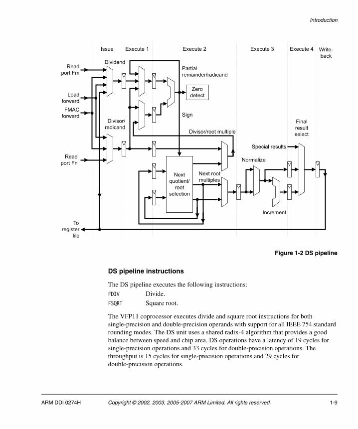
Figure 1-2 on page 1-9 shows the structure of the DS pipeline.
1-8 Copyright © 2002, 2003, 2005-2007 ARM Limited. All rights reserved. ARM DDI 0274H
Introduction
Figure 1-2 DS pipeline
DS pipeline instructions
The DS pipeline executes the following instructions:
FDIV Divide.
FSQRT Square root.
The VFP11 coprocessor executes divide and square root instructions for both single-precision and double-precision operands with support for all IEEE 754 standard rounding modes. The DS unit uses a shared radix-4 algorithm that provides a good balance between speed and chip area. DS operations have a latency of 19 cycles for single-precision operations and 33 cycles for double-precision operations. The throughput is 15 cycles for single-precision operations and 29 cycles for double-precision operations.
ARM DDI 0274H Copyright © 2002, 2003, 2005-2007 ARM Limited. All rights reserved. 1-9

Introduction
1.4.3 LS pipeline
Figure 1-3 shows the structure of the LS pipeline.
Figure 1-3 LS pipeline
The LS pipeline handles all of the instructions that involve data transfer to and from the ARM1136JF-S processor, including loads, stores, moves to coprocessor system registers, and moves from coprocessor system registers. It is synchronized with the ARM1136 processor LS pipeline for the duration of the instruction. Data written to the ARM1136 processor is read from the VFP11 coprocessor register file in the Issue stage and transferred to the ARM1136 processor in the next cycle and is latched on the ARM1136 data cache1 or data cache 2 cycle boundary. The transfer is made on a dedicated 64-bit store data bus between the VFP11 coprocessor and the ARM1136 processor. Load data is written to the VFP11 coprocessor on a dedicated 64-bit load data bus between the ARM1136 processor and all coprocessors. Data is received by the VFP11 coprocessor in the Writeback stage. Data is written to the register file in the Writeback stage, and available for forwarding to data processing operations in the same cycle.
1-10 Copyright © 2002, 2003, 2005-2007 ARM Limited. All rights reserved. ARM DDI 0274H

Introduction
LS pipeline instructions
The LS pipeline executes the following instructions:
FLD Load a single-precision, double-precision, or 32-bit integer value from memory to the VFP11 register file.
FLDM Load up to 32 single-precision or integer values or 16 double-precision values from memory to the VFP11 register file.
FST Store a single-precision, double-precision, or 32-bit integer value from the VFP11 register file to memory.
FSTM Store up to 32 single-precision or integer values or 16 double-precision values from the VFP11 register file to memory.
FMSR Move a single-precision or integer value from an ARM1136JF-S register to a VFP11 single-precision register.
FMRS Move a single-precision or integer value from a VFP11 single-precision register to an ARM1136JF-S register.
FMDHR Move an ARM1136JF-S register value to the upper half of a VFP11 double-precision register.
FMDLR Move an ARM1136JF-S register value to the lower half of a VFP11 double-precision register.
FMRDH Move the upper half of a double-precision value from a VFP11 double-precision register to an ARM1136JF-S register.
FMRDL Move the lower half of a double-precision value from a VFP11 double-precision register to an ARM1136JF-S register.
FMDRR Move two ARM1136JF-S register values to a VFP11 double-precision register.
FMRRD Move a double-precision VFP11 register value to two ARM1136JF-S registers.
FMSRR Move two ARM1136JF-S register values to two consecutively-numbered VFP11 single-precision registers.
FMRRS Move two consecutively-numbered VFP11 single-precision register values to two ARM1136JF-S registers.
FMXR Move an ARM1136JF-S register value to a VFP11 control register.
ARM DDI 0274H Copyright © 2002, 2003, 2005-2007 ARM Limited. All rights reserved. 1-11

Introduction
FMRX Move a VFP11 control register value to an ARM1136JF-S register.
FMSTAT Move N, C, Z, and V flags from the VFP11 FPSCR to the ARM1136JF-S CPSR.
1-12 Copyright © 2002, 2003, 2005-2007 ARM Limited. All rights reserved. ARM DDI 0274H

Introduction
1.5 Modes of operation
The VFP11 coprocessor provides compatibility with the IEEE 754 standard through a combination of hardware and software. There are rare cases that require significant additional compute time to resolve correctly to the requirements of the IEEE 754 standard. For instance, the VFP11 coprocessor does not process subnormal input values directly. To provide correct handling of subnormal inputs according to the IEEE 754 standard, a trap is made to support code to process the operation. Using the support code to process this operation might require hundreds of cycles. In some applications this is unavoidable, because compliance with the IEEE 754 standard is essential for the required operation of the program. In many other applications, strict compliance to the IEEE 754 standard is unnecessary, and determinable runtime, low interrupt latency, and low power are more important. To support a variety of applications, the VFP11 coprocessor provides four modes of operation, described in the following sections:
• Full-compliance mode
• Flush-to-zero mode on page 1-14
• Default NaN mode on page 1-15
• RunFast mode on page 1-15.
1.5.1 Full-compliance mode
When the VFP11 coprocessor is in full-compliance mode, all operations that cannot be processed according to the IEEE 754 standard use support code for assistance. The operations requiring support code are:
• Any Coprocessor Data Processing (CDP) operation involving a subnormal input when not in flush-to-zero mode.
• Any CDP operation involving a NaN input when not in default NaN mode.
• Any CDP operation that has the potential of generating an underflow condition when not in flush-to-zero mode.
• Any CDP operation when Inexact exceptions are enabled.
• Any CDP operation that can cause an overflow while Overflow exceptions are enabled.
• Any CDP operation that involves an invalid arithmetic operation or an arithmetic operation on a signaling NaN when Invalid Operation exceptions are enabled.
• A float-to-integer conversion that has the potential to create an integer that cannot be represented in the destination integer format when Invalid Operation exceptions are enabled.
ARM DDI 0274H Copyright © 2002, 2003, 2005-2007 ARM Limited. All rights reserved. 1-13

Introduction
You can avoid some of these support code requirements by:
• enabling flush-to-zero mode, by setting the FZ bit, FPSCR[24], to 1
• enabling default NaN mode, by setting the DN bit, FPSCR[25], to 1.
Some of the other support code requirements only occur when the appropriate feature is enabled. You enable:
• Inexact exceptions by setting the IXE bit, FPSCR[12], to 1
• Overflow exceptions by setting the OFE bit, FPSCR[10], to 1
• Invalid Operation exceptions by setting the IOE bit, FPSCR[8], to 1.
The support code:
• determines the nature of the exception
• determines if processing is required to perform the computation
• calls a function to compute the result and status
• transfers control to the user trap handler if the enable bit is set for a detected exception
• writes the result to the destination register, updates the FPSCR register, and returns to the user code if no enabled exception is detected
• passes control to the user trap handler and supplies any specified intermediate result for the exception if an enabled exception is detected.
Arithmetic exceptions on page 5-25 describes the conditions under which the VFP11 coprocessor traps to support code.
1.5.2 Flush-to-zero mode
Setting the FZ bit, FPSCR[24], to 1 enables flush-to-zero mode and increases performance on very small inputs and results. In flush-to-zero mode, the VFP11 coprocessor treats all subnormal input operands of arithmetic CDP operations as positive zeros in the operation. Exceptions that result from a zero operand are signaled appropriately. FABS, FNEG, FCPY, and FCMP are not considered arithmetic CDP operations and are not affected by flush-to-zero mode. A result that is tiny, as described in the IEEE 754 standard, for the destination precision is smaller in magnitude than the minimum normal value before rounding and is replaced with a positive zero. The IDC flag, FPSCR[7], indicates when an input flush occurs. The UFC flag, FPSCR[3], indicates when a result flush occurs.
1-14 Copyright © 2002, 2003, 2005-2007 ARM Limited. All rights reserved. ARM DDI 0274H

Introduction
1.5.3 Default NaN mode
Setting the DN bit, FPSCR[25], to 1 enables default NaN mode. In default NaN mode, the result of any operation that involves an input NaN or generated a NaN result returns the default NaN. Propagation of the fraction bits is maintained only by FABS, FNEG, and FCPY operations. All other CDP operations ignore any information in the fraction bits of an input NaN. See NaN handling on page 3-5 for a description of default NaNs.
1.5.4 RunFast mode
RunFast mode is the combination of the following conditions:
• the VFP11 coprocessor is in flush-to-zero mode
• the VFP11 coprocessor is in default NaN mode
• all exception enable bits are cleared to 0.
In RunFast mode the VFP11 coprocessor:
• Processes subnormal input operands as positive zeros
• Processes results that are tiny before rounding as positive zeros. A tiny result is one that is between the positive and negative minimum normal values for the destination precision.
• Processes input NaNs as default NaNs.
• Returns the default result specified by the IEEE 754 standard for the following conditions fully in hardware and without additional latency:
— overflow
— division by zero
— invalid operation
— inexact operation.
• Processes all operations in hardware without trapping to support code.
RunFast mode enables the programmer to write code for the VFP11 coprocessor that runs in a determinable time without support code assistance, regardless of the characteristics of the input data. In RunFast mode, no user exception traps are available. However, the exception flags in the FPSCR register comply with the IEEE 754 standard for Inexact, Overflow, Invalid Operation, and Division by Zero exceptions. The underflow flag is modified for flush-to-zero mode. Each of these flags is set by an exceptional condition and can by cleared only by a write to the FPSCR register.
ARM DDI 0274H Copyright © 2002, 2003, 2005-2007 ARM Limited. All rights reserved. 1-15

Introduction
1.6 Short vector instructions
The VFPv2 architecture supports execution of short vector instructions of up to eight operations on single-precision data and up to four operations on double-precision data. Short vectors are most useful in graphics and signal-processing applications. They reduce code size, increase speed of execution by supporting parallel operations and multiple transfers, and simplify algorithms with high data throughput. Short vector operations issue the individual operations specified in the instruction in a serial fashion. To eliminate data hazards, short vector operations begin execution only after all source registers are available, and all destination registers are not targets of other operations.
See Chapter 4 Instruction Execution for more information on execution of short vector instructions.
1-16 Copyright © 2002, 2003, 2005-2007 ARM Limited. All rights reserved. ARM DDI 0274H

Introduction
1.7 Parallel execution of instructions
The VFP11 coprocessor can execute several floating-point operations in parallel, while the ARM1136JF-S processor is executing ARM instructions. While a short vector operation executes for a number of cycles in the VFP11 coprocessor, it appears to the ARM1136 processor as a single-cycle instruction and is retired in the ARM1136 processor before it completes execution in the VFP11 coprocessor. The three pipelines in the VFP coprocessor operate independently of one another once initial processing is completed. This means you can issue a short vector operation, and issue a load or store multiple operation in the next cycle, and have both executing at the same time, provided no data hazards exist between the two instructions. With this mechanism, you can write algorithms that can be double-buffered to hide much of the time to transfer data to and from the VFP11 coprocessor under the arithmetic operations. This results in a significant improvement in performance. The separate DS pipeline enables both data transfer operations and CDPs that are not to the DS pipeline to execute in parallel with the divide. The DS block has a dedicated write port to the register file, and executing operations in parallel with divide or square root instructions does not require any special care. For more information see Parallel execution on page 4-24.
ARM DDI 0274H Copyright © 2002, 2003, 2005-2007 ARM Limited. All rights reserved. 1-17

Introduction
1.8 VFP11 treatment of branch instructions
The VFP11 coprocessor does not provide branch instructions directly. Instead, the result of a floating-point compare instruction can be stored in the ARM1136 condition code flags using the FMSTAT instruction. This means you can use the ARM1136 branch instructions and conditional execution capability for executing conditional floating-point code.
In some cases, full IEEE 754 standard comparisons are not required. You can make simple comparisons of single-precision data, such as comparisons to zero or to a constant, using an FMRS transfer and the ARM11 CMP and CMN instructions. This method is faster in many cases than using an FCMP instruction followed by an FMSTAT instruction. For more information, see Compliance with the IEEE 754 standard on page 3-3 and Comparisons on page 3-6.
1-18 Copyright © 2002, 2003, 2005-2007 ARM Limited. All rights reserved. ARM DDI 0274H

Introduction
1.9 Writing optimal VFP11 code
The following guidelines provide significant performance increases for VFP11 code:
• Unless there is a read-after-write hazard, program most scalar operations to immediately follow each other. Instead of a VFP11 FMAC instruction, use either a single ARM11 instruction or a VFP11 load or store instruction after the following instructions:
— a scalar double-precision multiply
— a multiply and accumulate
— a short vector instruction of length greater than one iteration.
• Avoid short vector divides and square roots. The VFP11 FMAC and DS pipelines are unavailable until the final iteration of the short vector DS operation issues from the Execute 1 stage. If the short vector DS operation can be separated, other VFP11 instructions can be issued in the cycles immediately following the divide or square root. See Parallel execution on page 4-24.
• For best performance in data-intensive applications, double-buffer looped short vector instructions. You can divide the register banks to provide multiple independent working areas. To take advantage of the simultaneous execution of data transfer and short vector arithmetic instructions, follow the arithmetic instructions on one bank with load or store instructions on the other bank.
• Moves to and from control registers are serializing. Avoid placing these in loops or time-critical code.
• If you do not require comparisons that are fully compliant with the IEEE 754 standard, avoid using FCMPE and FCMPEZ. Using an FMRS instruction with an ARM11 CMP or CMN can be faster for simple comparisons. See Comparisons on page 3-6.
ARM DDI 0274H Copyright © 2002, 2003, 2005-2007 ARM Limited. All rights reserved. 1-19

Introduction
1.10 Product revisions
See Product revision status on page xii for a description of revision numbering. This version of the VFP11 coprocessor is included in the r1p5 ARM1136JF-S processor release.
Note Previous releases of this manual described implementations of the VFP11 coprocessor which were common to more than one ARM processor. However:
• the ARM1176JZF-S Technical Reference Manual (ARM DDI0301) includes a full description of the version of the VFP11 coprocessor which forms part of that processor
• the ARM1156T2F-S Technical Reference Manual (ARM DDI0290) includes a full description of the version of the VFP11 coprocessor which forms part of that processor.
This means that, from issue E, this VFP11 coprocessor manual refers only to the coprocessor included with the ARM1136JF-S processor.
The changes made in the rev1 release of the VFP11 coprocessor are:
rev0 - rev1 Contains the following differences in functionality:
• addition of two Media and VFP Feature Registers
• update to the FPSID register to reflect the r1p0 release.
r1p0 - r1p5 There are no changes to the VFP11 coprocessor functionality between releases r1p0 and r1p5. The release number changes correspond to changes in the release number of the ARM1136JF-S processor, because of errata-fix releases.
Note • ARM1136JF-S processor releases r1p2 and r1p4 were not
generally available.
• The VFP coprocessor version number changes in ARM1136JF-S release r1p5. This is for consistency with the VFP coprocessor version numbers for other ARM11 processors, because of errata-fix updates. For details of the VFP version number see Floating-Point System ID Register, FPSID on page 3-17.
1-20 Copyright © 2002, 2003, 2005-2007 ARM Limited. All rights reserved. ARM DDI 0274H

Chapter 2 Register File
This chapter describes the VFP11 register file. It contains the following sections:
• About the register file on page 2-2
• Register file internal formats on page 2-3
• Decoding the register file on page 2-5
• Loading operands from ARM1136JF-S registers on page 2-6
• Maintaining consistency in register precision on page 2-8
• Data transfer between memory and VFP11 registers on page 2-9
• Access to register banks in CDP operations on page 2-11.
ARM DDI 0274H Copyright © 2002, 2003, 2005-2007 ARM Limited. All rights reserved. 2-1

Register File
2.1 About the register file
The register file is organized in four banks of eight 32-bit registers. Each register can store either a single-precision floating-point number or an integer.
Any consecutive pair of registers, [R2n+1]:[R2n], can store a double-precision floating-point number. Because a load and store operation does not modify the data, another application that does not use floating-point values can use the VFP11 registers as secondary data storage.
The register file can be configured as four circular buffers for use by short vector instructions in applications requiring high data throughput, such as filtering and graphics transforms. For short vector instructions, register addressing is circular in each bank. Because load and store operations do not circulate, you can load or store multiple banks, up to the entire register file, with a single instruction. Short vector operations obey certain rules specifying the conditions under which the registers in the argument list specify circular buffers or single-scalar registers. The LEN and STRIDE fields in the FPSCR register specify the number of operations performed by short vector instructions and the increment scheme in the circular register banks. See the ARM Architecture Reference Manual for more information.
2-2 Copyright © 2002, 2003, 2005-2007 ARM Limited. All rights reserved. ARM DDI 0274H

Register File
2.2 Register file internal formats
The VFPv2 architecture includes the option of an internal data format that is different from some or all of the external formats. In the VFP11 coprocessor, data in the register file has the same format as data in memory. Load or store operations for single-precision, double-precision, or integer data do not modify the format as a consequence of the transfer. However, to ensure compatibility with possible future VFP implementations, you must use FLDMX and FSTMX instructions when saving context and restoring VFP11 registers. See the ARM Architecture Reference Manual for more information.
When programming the VFP, you must be aware of the data type in each register. The hardware does not perform any checking of the agreement between the data type in the source registers and the data type expected by any instruction. Hardware always interprets the data according to the precision implied in the instruction.
Accessing a register that has not been initialized or loaded with valid data is Unpredictable. A way to detect access to an uninitialized register is to load all registers with Signaling NaNs (SNaNs) in the precision of the initial access of the register and enable the Invalid Operation exception.
2.2.1 Integer data format
The VFP11 coprocessor supports signed and unsigned 32-bit integers. It treats signed integers as two’s complement values. A load, store, or transfer operation on integer data does not imply any modification to the data. The format of integer data in the register file is identical to the format in memory and in an ARM11 general-purpose register.
2.2.2 Single-precision data format
Figure 2-1 shows the single-precision bit fields.
Figure 2-1 Single-precision data format
The single-precision data format contains:
• the sign bit, S, bit [31]
• the exponent, bits [30:23]
• the fraction, bits [22:0].
ARM DDI 0274H Copyright © 2002, 2003, 2005-2007 ARM Limited. All rights reserved. 2-3

Register File
The IEEE 754 standard defines the single-precision data format of the VFP11 coprocessor. See the IEEE 754 standard for information about exponent bias, special formats, and numerical ranges.
2.2.3 Double-precision data format
Double-precision format has a Most Significant Word (MSW) and a Least Significant Word (LSW). Figure 2-2 shows the double-precision bit fields.
Figure 2-2 Double-precision data format
The MSW contains:
• the sign bit, S, bit [31]
• the exponent, bits [30:20]
• the upper 20 bits of the fraction, bits [19:0].
The LSW contains the lower 32 bits of the fraction.
The IEEE 754 standard defines the double-precision data format used in the VFP11 coprocessor. See the IEEE 754 standard for details about exponent bias, special formats, and numerical ranges.
2-4 Copyright © 2002, 2003, 2005-2007 ARM Limited. All rights reserved. ARM DDI 0274H

Register File
2.3 Decoding the register file
Each register file access uses the five bits of the register number in the instruction word. For single-precision and integer accesses, the most significant four bits are in the Fm, Fn, or Fd field, and the least significant bit is the M, N, or D bit for each instruction format. For instructions with double-precision operands or destinations, the M, N, and D bit corresponding to a double-precision access must be zero. Figure 2-3 shows the register file. See the ARM Architecture Reference Manual for instruction formats and the positions of these bits.
Figure 2-3 Register file access
ARM DDI 0274H Copyright © 2002, 2003, 2005-2007 ARM Limited. All rights reserved. 2-5

Register File
2.4 Loading operands from ARM1136JF-S registers
Use the MCR, MRC, MCRR, and MRRC coprocessor data transfer instructions to transfer floating-point data between ARM1136 registers and VFP11 registers. No exceptions are possible on these transfer instructions.
MCR instructions transfer 32-bit values from ARM1136 registers to VFP11 registers as Table 2-1 shows.
MRC instructions transfer 32-bit values from VFP11 registers to ARM1136 registers as Table 2-2 shows.
Table 2-1 VFP11 MCR instructions
Instruction Operation Description
FMXR VFP11 system register = Rd Move from ARM1136 register Rd to VFP11 system register FPSIDa, FPSCR, FPEXC, FPINST, or FPINST2.
FMDLR Dn[31:0] = Rd Move from ARM1136 register Rd to lower half of VFP11 double-precision register Dn.
FMDHR Dn[63:32] = Rd Move from ARM1136 register Rd to upper half of VFP11 double-precision register Dn.
FMSR Sn = Rd Move from ARM1136 register Rd to VFP11 single-precision or integer register Sn.
a. Writing to the FPSID register does not change the contents of the FPSID but may be used as a serializing instruction.
Table 2-2 VFP11 MRC instructions
Instruction Operation Description
FMRX Rd = VFP11 system register Move from VFP11 system register FPSID, FPSCR, FPEXC, FPINST, or FPINST2 to ARM1136 register Rd.
FMRDL Rd = Dn[31:0] Move from lower half of VFP11 double-precision register Dn to ARM1136 register Rd.
FMRDH Rd = Dn[63:32] Move from upper half of VFP11 double-precision register Dn to ARM1136 register Rd.
FMRS Rd = Sn Move from VFP11 single-precision or integer register Sn to ARM1136 register Rd.
2-6 Copyright © 2002, 2003, 2005-2007 ARM Limited. All rights reserved. ARM DDI 0274H
Register File
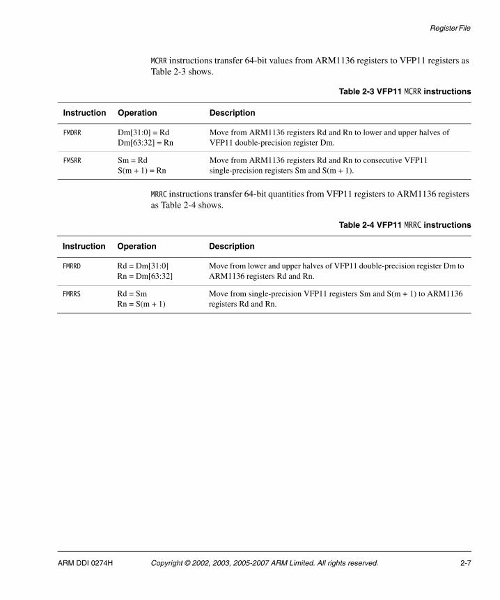
MCRR instructions transfer 64-bit values from ARM1136 registers to VFP11 registers as Table 2-3 shows.
MRRC instructions transfer 64-bit quantities from VFP11 registers to ARM1136 registers as Table 2-4 shows.
Table 2-3 VFP11 MCRR instructions
Instruction Operation Description
FMDRR Dm[31:0] = Rd Dm[63:32] = Rn
Move from ARM1136 registers Rd and Rn to lower and upper halves of VFP11 double-precision register Dm.
FMSRR Sm = Rd S(m + 1) = Rn
Move from ARM1136 registers Rd and Rn to consecutive VFP11 single-precision registers Sm and S(m + 1).
Table 2-4 VFP11 MRRC instructions
Instruction Operation Description
FMRRD Rd = Dm[31:0] Rn = Dm[63:32]
Move from lower and upper halves of VFP11 double-precision register Dm to ARM1136 registers Rd and Rn.
FMRRS Rd = Sm Rn = S(m + 1)
Move from single-precision VFP11 registers Sm and S(m + 1) to ARM1136 registers Rd and Rn.
ARM DDI 0274H Copyright © 2002, 2003, 2005-2007 ARM Limited. All rights reserved. 2-7

Register File
2.5 Maintaining consistency in register precision
The VFP11 register file stores single-precision, double-precision, and integer data in the same registers. For example, D6 occupies the same registers as S12 and S13. The usable format of the register or registers depends on the last load or arithmetic instruction that wrote to the register or registers.
The VFP11 hardware does not check the register format to see if it is consistent with the precision of the current operation. Inconsistent use of the registers is possible but Unpredictable. The hardware interprets the data in the format required by the instruction regardless of the latest store or write operation to the register. The compiler or programmer must maintain consistency in register usage.
2-8 Copyright © 2002, 2003, 2005-2007 ARM Limited. All rights reserved. ARM DDI 0274H

Register File
2.6 Data transfer between memory and VFP11 registers
The B bit in the CP15 c1 Control Register determines whether access to stored memory is little-endian or big-endian. See the ARM Architecture Reference Manual for details of this register. The ARM1136JF-S processor supports both little-endian and big-endian access formats in memory.
The ARM1136 processor stores 32-bit words in memory with the Least Significant Byte (LSB) in the lowest byte of the memory address regardless of the endianness selected. For a store of a single-precision floating-point value, the LSB is located at the target address with the lower two bits of the address cleared to b00. The Most Significant Byte (MSB) is at the target address with the lower two bits set to b11. For best performance, all single-precision data must be aligned in memory to four-byte boundaries, and double-precision data must be aligned to eight-byte boundaries.
Table 2-5 shows how single-precision data is stored in memory and the address to access each byte in both little-endian and big-endian formats. In this example, the target address is 0x40000000.
For double-precision data, the location of the two words that comprise the data are different for little-endian and big-endian data access formats. Table 2-6 shows the data storage in memory and the address to access each byte in little-endian and big-endian access modes. In this example, the target address is 0x40000000.
Table 2-5 Single-precision data memory images and byte addresses
Single-precision data bytes
Address in memory
Little-endian byte address
Big-endian byte address
MSB, bits [31:24] 0x40000003 0x40000003 0x40000000
Bits [23:16] 0x40000002 0x40000002 0x40000001
Bits [15:8] 0x40000001 0x40000001 0x40000002
LSB, bits [7:0] 0x40000000 0x40000000 0x40000003
Table 2-6 Double-precision data memory images and byte addresses
Double- precisiondata bytes
Little-endianaddress in memory
Little-endian byte address
Big-endianaddress in memory
Big-endian byte address
MSB, bits [63:56] 0x40000007 0x40000007 0x40000003 0x40000000
Bits [55:48] 0x40000006 0x40000006 0x40000002 0x40000001
Bits [47:40] 0x40000005 0x40000005 0x40000001 0x40000002
ARM DDI 0274H Copyright © 2002, 2003, 2005-2007 ARM Limited. All rights reserved. 2-9

Register File
In each data word, the memory image for the data is identical for the little-endian and big-endian formats. The ARM1136 hardware performs the address transformations to provide both little-endian and big-endian addressing to the programmer.
Bits [39:32] 0x40000004 0x40000004 0x40000000 0x40000003
Bits [31:24] 0x40000003 0x40000003 0x40000007 0x40000004
Bits [23:16] 0x40000002 0x40000002 0x40000006 0x40000005
Bits [15:8] 0x40000001 0x40000001 0x40000005 0x40000006
LSB, bits [7:0] 0x40000000 0x40000000 0x40000004 0x40000007
Table 2-6 Double-precision data memory images and byte addresses (continued)
Double- precisiondata bytes
Little-endianaddress in memory
Little-endian byte address
Big-endianaddress in memory
Big-endian byte address
2-10 Copyright © 2002, 2003, 2005-2007 ARM Limited. All rights reserved. ARM DDI 0274H

Register File
2.7 Access to register banks in CDP operations
The register file is particularly suitable for short vector operations. The four register banks function as four circular hardware queues. Short vector operations significantly improve the performance of operations with high data throughput such as signal processing and matrix manipulation functions.
2.7.1 About register banks
Figure 2-4 shows how the register file is divided into four banks, with eight registers in each bank for single-precision instructions and four registers per bank for double-precision instructions. CDP instructions access the banks in a circular manner. Load and store multiple instructions do not access the registers in a circular manner but treat the register file as a linearly-ordered structure.
See the ARM Architecture Reference Manual for more information about VFP addressing.
Figure 2-4 Register banks
A short vector CDP operation that has a source or destination vector crossing a bank boundary wraps around and accesses the first register in the bank.
Example 2-1 on page 2-12 shows the iterations of the following short vector add instruction:
FADDS S11, S22, S31
In this instruction, the LEN field contains b101, selecting a vector length of six iterations, and the STRIDE field contains b00, selecting a vector stride of one.
ARM DDI 0274H Copyright © 2002, 2003, 2005-2007 ARM Limited. All rights reserved. 2-11

Register File
Example 2-1 Register bank wrapping
FADDS S11, S22, S31 ; 1st iteration FADDS S12, S23, S24 ; 2nd iteration. The 2nd source vector wraps around
; and accesses the 1st register in the 4th bankFADDS S13, S16, S25 ; 3rd iteration. The 1st source vector wraps around
; and accesses the 1st register in the 3rd bankFADDS S14, S17, S26 ; 4th iterationFADDS S15, S18, S27 ; 5th iterationFADDS S8, S19, S28 ; 6th and last iteration. The destination vector
; wraps around and writes to the 1st register in the; 2nd bank
2.7.2 Operations using register banks
The register file organization supports four types of operation, described in the following sections:
• Scalar-only instructions
• Short vector-only instructions on page 2-13
• Short vector instructions with scalar source on page 2-13
• Scalar instructions in short vector mode on page 2-14.
See Floating-Point Status and Control Register, FPSCR on page 3-18 for details of the LEN and STRIDE fields and the FPSCR register.
Scalar-only instructions
An instruction is a scalar-only operation if the operands are treated as scalars and the result is a scalar.
Clearing the LEN field in the FPSCR register to zero selects a vector length of one iteration. For example, if the LEN field contains b000, then the following operation writes the sum of the single-precision values in S21 and S22 to S12:
FADDS S12, S21, S22
Some instructions can operate only on scalar data regardless of the value in the LEN field. These instructions are:
Compare operations
FCMPS and FCMPD, FCMPZS and FCMPZD, FCMPES and FCMPED, FCMPEZS and FCMPEZD.
2-12 Copyright © 2002, 2003, 2005-2007 ARM Limited. All rights reserved. ARM DDI 0274H

Register File
Integer conversions
FTOUIS and FTOUID, FTOUIZS and FTOUIZD, FTOSIS and FTOSID, FTOSIZS and FTOSIZD, FUITOS and FUITOD, FSITOS and FSITOD.
Precision conversions
FCVTDS and FCVTSD.
Short vector-only instructions
Vector-only instructions require that the value in the LEN field is nonzero, and that the destination and Fm registers are not in bank 0.
Example 2-2 shows the iterations of the following short vector instruction:
FMACS S16, S0, S8
In the example, the LEN field contains b011, selecting a vector length of four iterations, and the STRIDE field contains b00, selecting a vector stride of one.
Example 2-2 Short vector instruction
FMACS S16, S0, S8 ; 1st iterationFMACS S17, S1, S9 ; 2nd iterationFMACS S18, S2, S10 ; 3rd iterationFMACS S19, S3, S11 ; 4th and last iteration
Short vector instructions with scalar source
In the VFPv2 architecture, a scalar operand can operate on a vector. The destination must be a vector, that is, not in bank 0, and the Fm operand must be in bank 0.
Example 2-3 on page 2-14 shows the iterations of the following short vector instruction with a scalar source:
FMULD D12, D8, D2
In the example, the LEN field contains b001, selecting a vector length of two iterations, and the STRIDE field contains b00, selecting a vector stride of one.
ARM DDI 0274H Copyright © 2002, 2003, 2005-2007 ARM Limited. All rights reserved. 2-13

Register File
Example 2-3 Short vector instruction with scalar source
FMULD D12, D8, D2 ; 1st iterationFMULD D13, D9, D2 ; 2nd and last iteration
This scales the two source registers, D8 and D9, by the value in D2 and writes the new values to D12 and D13.
Scalar instructions in short vector mode
You can mix scalar and short vector operations by carefully selecting the source and destination registers. If the destination is in bank 0, the operation is scalar-only regardless of the value in the LEN field. You do not have to change the LEN field from a nonzero value to b000 to perform scalar operations.
Example 2-4 shows the sequence of operations for the following instructions:
FABSD D4, D8FADDS S0, S0, S31FMULS S24, S26, S1
In the example, the LEN field contains b001, selecting a vector length of two iterations, and the STRIDE field contains b00, selecting a vector stride of one.
Example 2-4 Scalar operation in short vector mode
FABSD D4, D8 ; vector DP ABS operation on regs (D8, D9) to (D4, D5)FABSD D5, D9FADDS S0, S0, S31 ; scalar increment of S0 by S31FMULS S24, S26, S1 ; vector (S26, S27) scaled by S1 and written to (S24, S25)FMULS S25, S27, S1
Table 2-7 on page 2-15 to Table 2-10 on page 2-16 show the four types of operations possible in the VFPv2 architecture. In the tables:
Any Refers to the availability of all registers in the precision for the specified operand.
S Refers to a scalar operand with only a single register.
V Refers to a vector operand with multiple registers.
2-14 Copyright © 2002, 2003, 2005-2007 ARM Limited. All rights reserved. ARM DDI 0274H

Register File
Table 2-7 describes single-precision three-operand register usage.
Table 2-8 describes single-precision two-operand register usage.
Table 2-9 describes double-precision three-operand register usage.
Table 2-7 Single-precision three-operand register usage
LEN field Fd Fn Fm Operation type
b000 Any Any Any S = S op S OR S = S S S
Nonzero 0-7 Any Any S = S op S OR S = S S S
8-31 Any 0-7 V = V op S OR V = V V S
8-31 V = V op V OR V = V V V
Table 2-8 Single-precision two-operand register usage
LEN field Fd Fm Operation type
b000 Any Any S = op S
Nonzero 0-7 Any S = op S
8-31 0-7 V = op S
8-31 V = op V
Table 2-9 Double-precision three-operand register usage
LEN field Fd Fn Fm Operation type
b000 Any Any Any S = S op S OR S = S S S
Nonzero 0-3 Any Any S = S op S OR S = S S S
4-15 Any 0-3 V = V op S OR V = V V S
4-15 V = V op V OR V = V V V
ARM DDI 0274H Copyright © 2002, 2003, 2005-2007 ARM Limited. All rights reserved. 2-15

Register File
Table 2-10 describes double-precision two-operand register usage.
Table 2-10 Double-precision two-operand register usage
LEN field Fd Fm Operation type
b000 Any Any S = op S
Nonzero 0-3 Any S = op S
4-15 0-3 V = op S
4-15 V = op V
2-16 Copyright © 2002, 2003, 2005-2007 ARM Limited. All rights reserved. ARM DDI 0274H

Chapter 3 Programmer’s Model
This chapter describes implementation-specific features of the VFP11 coprocessor that are useful to programmers. It contains the following sections:
• About the programmer’s model on page 3-2
• Compliance with the IEEE 754 standard on page 3-3
• ARMv5TE coprocessor extensions on page 3-9
• VFP11 system registers on page 3-15.
ARM DDI 0274H Copyright © 2002, 2003, 2005-2007 ARM Limited. All rights reserved. 3-1

Programmer’s Model
3.1 About the programmer’s model
This section introduces the VFP11 implementation of the VFPv2 floating-point architecture.
Note The ARM Architecture Reference Manual describes the VFPv1 architecture.
The VFP11 coprocessor implements all the instructions and modes of the VFPv2 architecture. The VFPv2 architecture adds the following features and enhancements to the VFPv1 architecture:
• The ARM v5TE instruction set. This includes the MRRC and MCRR instructions to transfer 64-bit data between the ARM1136JF-S processor and the VFP11 coprocessor. These instructions allow the transfer of a double-precision register or two consecutively numbered single-precision registers to or from a pair of ARM1136 registers. See Loading operands from ARM1136JF-S registers on page 2-6 for syntax and usage of VFP MRRC and MCRR instructions.
• Default NaN mode. In default NaN mode, any operation involving one or more NaN operands produces the default NaN as a result, rather than returning the NaN or one of the NaNs involved in the operation. This mode is compatible with the IEEE 754 standard but not with current handling of NaNs by industry.
• Addition of the input subnormal flag, IDC, FPSCR[7]. The IDC flag is set to 1 whenever the VFP11 coprocessor is in flush-to-zero mode and a subnormal input operand is replaced by a positive zero. It remains set until cleared to 0 by writing to the FPSCR register. A new Input Subnormal exception enable bit, IDE, FPSCR[15], is also added. When IDE is set to 1, the VFP11 coprocessor traps to the Undefined trap handler for an instruction that has a subnormal input operand.
• New functionality for the underflow flag, UFC, FPSCR[3], in flush-to-zero mode. In flush-to-zero mode, UFC is set to 1 whenever a result is below the threshold for normal numbers before rounding, and the result is flushed to zero. UFC remains set until cleared to 0 by writing to the FPSCR register. Setting the Underflow exception enable bit, UFE, FPSCR[11], to 1 does not cause a trap in flush-to-zero mode.
• New functionality for the inexact flag, IXC, FPSCR[4], in flush-to-zero mode. In VFPv1, IXC is set to 1 when an input or result is flushed to zero. In VFPv2, the IDC and UFC flags provide this information. See Inexact exception on page 5-23 for more information.
• Addition of RunFast mode. For more information see RunFast mode on page 1-15.
3-2 Copyright © 2002, 2003, 2005-2007 ARM Limited. All rights reserved. ARM DDI 0274H

Programmer’s Model
3.2 Compliance with the IEEE 754 standard
This section introduces issues related to compliance with the IEEE 754 standard for:
• hardware and software components
• software-based components and their availability.
For more information about VFP architecture compliance with the IEEE 754 standard see the ARM Architecture Reference Manual.
3.2.1 An IEEE 754 standard-compliant implementation
The VFP11 hardware and support code together provide VFPv2 floating-point instruction implementations that comply with the IEEE 754 standard. Unless an enabled floating-point exception occurs, it appears to the program that the floating-point instruction was executed by the hardware. If an exceptional condition occurs that requires software support during instruction execution, the instruction takes significantly more cycles than normal to produce the result. This is a common practice in the industry, and the incidence of such instructions is typically very low.
3.2.2 Complete implementation of the IEEE 754 standard
The following operations from the IEEE 754 standard are not supplied by the VFP11 instruction set:
• remainder
• round floating-point number to integer-valued floating-point number
• binary-to-decimal conversions
• decimal-to-binary conversions
• direct comparison of single-precision and double-precision values.
For complete implementation of the IEEE 754 standard, the VFP11 coprocessor and support code must be augmented with library functions that implement these operations. See Application Note 98, VFP Support Code for details of support code and the available library functions.
3.2.3 IEEE 754 standard implementation choices
The ARM Architecture Reference Manual describes some of the implementation choices specified in the IEEE 754 standard and used in the VFPv2 architecture.
The VFP11 coprocessor includes further implementation choices about which cases are handled by the VFP11 hardware and which cases bounce to the support code.
ARM DDI 0274H Copyright © 2002, 2003, 2005-2007 ARM Limited. All rights reserved. 3-3

Programmer’s Model
To execute frequently encountered operations as fast as possible and minimize silicon area, handling of rarely occurring values and some exceptions is relegated to the support code. The VFP11 coprocessor supports two modes for handling rarely occurring values:
Full-compliance mode
Full-compliance mode with support code assistance is fully compliant with the IEEE 754 standard. Full-compliance mode requires the floating-point support code to handle certain operands and exceptional conditions not supported in the hardware. Although the support code gives full compliance with the IEEE 754 standard, it does increase the runtime of an application and the size of kernel code.
RunFast mode
In RunFast mode, default handling of subnormal inputs, underflows, and NaN inputs is not fully compliant with the IEEE 754 standard. No user trap handlers are allowed in RunFast mode.
When flush-to-zero and default NaN modes are enabled, and all exceptions are disabled, the VFP11 coprocessor operates in RunFast mode. While there is a potential loss of accuracy for very small values, RunFast mode removes a significant number of performance-limiting stall conditions. By not requiring the floating-point support code, RunFast mode provides increased performance of typical and optimized code and a reduction in the size of kernel code. See Hazards on page 4-7 for more information on performance improvements in RunFast mode.
Supported formats
The supported formats are:
• Single-precision and double-precision. No extended format is supported.
• Integer formats:
— unsigned 32-bit integers
— two’s complement signed 32-bit integers.
3-4 Copyright © 2002, 2003, 2005-2007 ARM Limited. All rights reserved. ARM DDI 0274H

Programmer’s Model
NaN handling
Any single-precision or double-precision values with the maximum exponent field value and a nonzero fraction field are valid NaNs. A most significant fraction bit of zero indicates a Signaling NaN (SNaN). A most significant fraction bit of one indicates a Quiet NaN (QNaN). Two NaN values are treated as different NaNs if they differ in any bit. Table 3-1 shows the default NaN values in both single and double precision.
Any SNaN passed as input to an operation causes an Invalid Operation exception and sets the IOC flag, FPSCR[0], to 1. If the IOE bit, FPSCR[8], is set to 1, control passes to a user trap handler if present. If IOE is not set to 1, a default QNaN is written to the destination register. See the ARM Architecture Reference Manual for the rules for cases involving multiple NaN operands.
Processing of input NaNs for ARM floating-point coprocessors and libraries is defined as follows:
• In full-compliance mode, NaNs are handled according to the ARM Architecture Reference Manual. The hardware does not process the NaNs directly for arithmetic CDP instructions, but traps to the support code for all NaN processing. For data transfer operations, NaNs are transferred without raising the Invalid Operation exception or trapping to support code. For the nonarithmetic CDP instructions, FABS, FNEG, and FCPY, NaNs are copied, with a change of sign if specified in the instructions, without causing the Invalid Operation exception or trapping to support code.
• In default NaN mode, NaNs are handled completely in the hardware without support code assistance. SNaNs in an arithmetic CDP operation set the IOC flag, FPSCR[0], to 1. NaN handling by data transfer and nonarithmetic CDP instructions is the same as in full-compliance mode. Arithmetic CDP instructions involving NaN operands return the default NaN regardless of the fractions of any NaN operands.
Table 3-1 Default NaN values
Single-precision Double-precision
Sign 0 0
Exponent 0xFF 0x7FF
Fraction Bit [22] = 1
Bits [21:0] are all zeros
Bit [51] = 1
Bits [50:0] are all zeros
ARM DDI 0274H Copyright © 2002, 2003, 2005-2007 ARM Limited. All rights reserved. 3-5

Programmer’s Model
Table 3-2 summarizes the effects of NaN operands on instruction execution.
Comparisons
Comparison results modify condition code flags in the FPSCR register. The FMSTAT instruction transfers the current condition code flags in the FPSCR register to the ARM1136 CPSR register. The condition code flags used are chosen so that subsequent conditional execution of ARM instructions can test the predicates defined in the IEEE 754 standard.
The VFP11 coprocessor handles most comparisons of numeric values in hardware, generating the appropriate condition code depending on whether the result is less than, equal to, or greater than. When the VFP11 coprocessor is not in flush-to-zero mode, comparisons involving subnormal operands bounce to support code.
Table 3-2 QNaN and SNaN handling
Instruction type
Default NaN mode With QNaN operand With SNaN operand
Arithmetic CDP
Off INVa set to 1. Bounce to support code to process operation.
On No bounce. Default NaN returns. IOCb set to 1. If IOEc set to 1, bounce to Invalid Operation user trap handler. If IOE set to 0, default NaN returns.
Nonarithmetic CDP
OffNaN passes to destination with sign changed as appropriate.
On
FCMP(Z)
Off INVa set to 1 to 1. Bounce to support code to process operation.
On No bounce. Unordered compare. IOCb set to 1. If IOEc set to 1, bounce to Invalid Operation user trap handler. If IOE set to 0, unordered compare.
FCMPE(Z)
Off INVa set to 1. Bounce to support code to process operation.
On IOCb set to 1. If IOEc set to 1, bounce to Invalid Operation user trap handler. If IOE set to 0, unordered compare.
Load/storeOff
All NaNs transferred. No bounce.On
a. INV is the Input exception flag, FPEXC[7].b. IOC is the Invalid Operation exception flag, FPSCR[0].c. IOE is the Invalid Operation exception enable bit, FPSCR[8].
3-6 Copyright © 2002, 2003, 2005-2007 ARM Limited. All rights reserved. ARM DDI 0274H
Programmer’s Model
The VFP11 coprocessor supports:
Compare operations
The compare operations are FCMPS, FCMPZS, FCMPD, and FCMPZD.
In default NaN mode, a compare instruction involving a QNaN produces an unordered result. An SNaN produces an unordered result and generates an Invalid Operation exception. If the IOE bit, FPSCR[8], is set to 1, the Invalid Operation user trap handler is called. When the VFP11 coprocessor is not in default NaN mode, comparisons involving NaNs bounce to support code.
Compare with exception operations
The compare with exception operations are FCMPES, FCMPEZS, FCMPED, and FCMPEZD.
In default NaN mode, a compare with exception operation involving either an SNaN or a QNaN produces an unordered result and generates an Invalid Operation exception. When the VFP11 coprocessor is not in default NaN mode, comparisons involving NaNs bounce to support code.
Some simple comparisons on single-precision data can be computed directly by the ARM1136 processor. If only equality or comparison to zero is required, and NaNs are not an issue, performing the comparison in ARM1136 registers using CMP or CMN instructions can be faster.
If branching on the state of the Z flag is required, you can use the following instructions for positive values:
FMRS Rx, SnCMP Rx, #0BEQ label
If the input values can include negative numbers, including negative zero, you can use the following code:
FMRS Rx, SnCMP Rx, #0x80000000CMPNE Rx, #0BEQ label
Using a temporary register is even faster:
FMRS Rx, SnMOVS Rt, Rx, LSL #1BEQ label
Comparisons with particular values are also possible. For example, to check if a positive value is greater or equal to +1.0, use:
ARM DDI 0274H Copyright © 2002, 2003, 2005-2007 ARM Limited. All rights reserved. 3-7

Programmer’s Model
FMRS Rx,SnCMP Rx,#0x3F800000BGE label
When comparisons are required for double-precision values, or when IEEE 754 standard comparisons are required, it is safer to use the FCMP and FCMPE instructions with FMSTAT.
Underflow
In the generation of Underflow exceptions, the after rounding form of tininess and the subnormalization loss form of loss of accuracy as described in the IEEE 754 standard are used.
In flush-to-zero mode, results that are tiny before rounding, as described in the IEEE 754 standard, are flushed to a positive zero, and the UFC flag, FPSCR[3], is set to 1. Support code is not involved. For more information on flush-to-zero mode see the ARM Architecture Reference Manual.
When the VFP11 coprocessor is not in flush-to-zero mode, any operation with a risk of producing a tiny result bounces to support code. If the operation does not produce a tiny result, it returns the computed result, and the UFC flag, FPSCR[3], is not set. The IXC flag, FPSCR[4], is set to 1 if the operation is inexact. If the operation produces a tiny result, the result is a subnormal or zero value, and the UFC flag, FPSCR[3], is set to 1. See Underflow exception on page 5-21 for more information on underflow handling.
Exceptions
The VFP11 coprocessor takes exceptions in an imprecise manner. When exception processing begins, the states of the ARM1136 processor and the VFP11 coprocessor might not be the same as when the exception occurred. Exceptional instructions cause the VFP11 coprocessor to enter the exceptional state, and the next VFP11 instruction triggers exception processing. After the issue of the exceptional instruction and before exception processing begins, non-VFP11 instructions and some VFP11 instructions can be executed and retired. The coprocessor preserves any source registers involved in the exceptional instruction, and the destination register is not overwritten on entry to the support code. If the detected exception enable bit is not set to 1, the support code returns to the program flow at the point of the trigger instruction after processing the exception. If the detected exception enable bit is set to 1, and a user trap handler is installed, the support code passes control to the user trap handler. If the exception is overflow or underflow, the intermediate result specified by the IEEE 754 standard is made available to the user trap handler.
3-8 Copyright © 2002, 2003, 2005-2007 ARM Limited. All rights reserved. ARM DDI 0274H

Programmer’s Model
3.3 ARMv5TE coprocessor extensions
This section describes the syntax and usage of the four ARMv5TE architecture coprocessor extension instructions: The instructions are described in the following sections:
• FMDRR
• FMRRD on page 3-10
• FMSRR on page 3-11
• FMRRS on page 3-13.
Note These instructions are implementations of the MCRR and MRRC instructions, described in the ARM Architecture Reference Manual.
3.3.1 FMDRR
FMDRR transfers data from two ARM1136 registers to a VFP11 double-precision register. The ARM1136 registers do not have to be contiguous. Figure 3-1 shows the format of the FMDRR instruction.
Figure 3-1 FMDRR instruction format
Syntax
FMDRR {<cond>} <Dm>, <Rd>, <Rn>
where:
<cond> Is the condition under which the instruction is executed. If <cond> is omitted, the AL (always) condition is used.
<Dm> Specifies the destination double-precision VFP11 coprocessor register.
<Rd> Specifies the source ARM1136 register for the lower 32 bits of the operand.
<Rn> Specifies the source ARM1136 register for the upper 32 bits of the operand.
ARM DDI 0274H Copyright © 2002, 2003, 2005-2007 ARM Limited. All rights reserved. 3-9

Programmer’s Model
Architecture version
D variants only
Exceptions
None
Operation
if ConditionPassed(cond) thenDm[upper half] = RnDm[lower half] = Rd
Notes
Conversions In the programmer’s model, FMDRR does not perform any conversion of the value transferred. Arithmetic instructions using either Rd or Rn treat the value as an integer, whereas most VFP instructions treat the Dm value as a double-precision floating-point number.
3.3.2 FMRRD
FMRRD transfers data in a VFP11 double-precision register to two ARM1136 registers. The ARM1136 registers do not have to be contiguous. Figure 3-2 shows the format of the FMRRD instruction.
Figure 3-2 FMRRD instruction format
Syntax
FMRRD {<cond>} <Rd>, <Rn>, <Dm>
where:
<cond> Is the condition under which the instruction is executed. If <cond> is omitted, the AL (always) condition is used.
<Rd> Specifies the destination ARM1136 register for the lower 32 bits of the operand.
3-10 Copyright © 2002, 2003, 2005-2007 ARM Limited. All rights reserved. ARM DDI 0274H

Programmer’s Model
<Rn> Specifies the destination ARM1136 register for the upper 32 bits of the operand.
<Dm> Specifies the source double-precision VFP11 coprocessor register.
Architecture version
D variants only
Exceptions
None
Operation
if ConditionPassed(cond) thenRn = Dm[upper half]Rd = Dm[lower half]
Notes
Use of r15 If r15 is specified for <Rd> or <Rn>, the results are Unpredictable.
Conversions In the programmer’s model, FMRRD does not perform any conversion of the value transferred. Arithmetic instructions using Rd and Rn treat the contents as an integer, whereas most VFP instructions treat the Dm value as a double-precision floating-point number.
3.3.3 FMSRR
FMSRR transfers data in two ARM1136 registers to two consecutively numbered single-precision VFP11 registers, Sm and S(m + 1). The ARM1136 registers do not have to be contiguous. Figure 3-3 shows the format of the FMSRR instruction.
Figure 3-3 FMSRR instruction format
ARM DDI 0274H Copyright © 2002, 2003, 2005-2007 ARM Limited. All rights reserved. 3-11

Programmer’s Model
Syntax
FMSRR {<cond>} <registers>, <Rd>, <Rn>
where:
<cond> Is the condition under which the instruction is executed. If <cond> is omitted, the AL (always) condition is used.
<registers> Specifies the pair of consecutively numbered single-precision destination VFP11 registers, separated by a comma and surrounded by brackets. If m is the number of the first register in the list, the list is encoded in the instruction by setting Sm to the top four bits of m and M to the bottom bit of m. For example, if <registers> is {S1, S2}, the Sm field of the instruction is b0000 and the M bit is 1.
<Rd> Specifies the source ARM1136 register for the Sm VFP11 single-precision register.
<Rn> Specifies the source ARM1136 register for the S(m + 1) VFP11 single-precision register.
Architecture version
All
Exceptions
None
Operation
If ConditionPassed(cond) thenSm = RdS(m + 1) = Rn
Notes
Conversions In the programmer’s model, FMSRR does not perform any conversion of the value transferred. Arithmetic instructions using Rd and Rn treat the contents as an integer, whereas most VFP instructions treat the Sm and S(m + 1) values as single-precision floating-point numbers.
3-12 Copyright © 2002, 2003, 2005-2007 ARM Limited. All rights reserved. ARM DDI 0274H

Programmer’s Model
Invalid register lists
If Sm is b1111 and M is 1 (an encoding of S31) the instruction is Unpredictable.
3.3.4 FMRRS
FMRRS transfers data in two consecutively numbered single-precision VFP11 registers to two ARM1136 registers. The ARM1136 registers do not have to be contiguous. Figure 3-4 shows the format of the FMRRS instruction.
Figure 3-4 FMRRS instruction format
Syntax
FMRRS {<cond>} <Rd>, <Rn>, <registers>
where:
<cond> Is the condition under which the instruction is executed. If <cond> is omitted, the AL (always) condition is used.
<Rd> Specifies the destination ARM1136 register for the Sm VFP11 coprocessor single-precision value.
<Rn> Specifies the destination ARM1136 register for the S(m + 1) VFP11 coprocessor single-precision value.
<registers> Specifies the pair of consecutively numbered single-precision VFP11 source registers, separated by a comma and surrounded by brackets. If m is the number of the first register in the list, the list is encoded in the instruction by setting Sm to the top four bits of m and M to the bottom bit of m. For example, if <registers> is {S16, S17}, the Sm field of the instruction is b1000 and the M bit is 0.
Architecture version
All
ARM DDI 0274H Copyright © 2002, 2003, 2005-2007 ARM Limited. All rights reserved. 3-13

Programmer’s Model
Exceptions
None
Operation
If ConditionPassed(cond) thenRd = SmRn = S(m + 1)
Notes
Conversions In the programmer’s model, FMRRS does not perform any conversion of the value transferred. Arithmetic instructions using Rd and Rn treat the contents as an integer, whereas most VFP11 instructions treat the Sm and S(m + 1) values as single-precision floating-point numbers.
Invalid register lists
If Sm is b1111 and M is 1 (an encoding of S31) the instruction is Unpredictable.
Use of r15 If r15 is specified for Rd or Rn, the results are Unpredictable.
3-14 Copyright © 2002, 2003, 2005-2007 ARM Limited. All rights reserved. ARM DDI 0274H

Programmer’s Model
3.4 VFP11 system registers
The VFPv2 architecture describes the following three system registers that must be present in a VFP system:
• Floating-Point System ID Register, FPSID
• Floating-Point Status and Control Register, FPSCR
• Floating-Point Exception Register, FPEXC.
The VFP11 coprocessor provides sufficient information for processing all exceptional conditions encountered by the hardware. In an exceptional situation, the hardware provides:
• the exceptional instruction
• the instruction issued to the VFP11 coprocessor before detection of the exception
• exception status information:
— type of exception
— number of remaining short vector iterations after an exceptional iteration.
To support exceptional conditions, the VFP11 coprocessor provides two additional registers:
• Floating-Point Instruction Register, FPINST
• Floating-Point Instruction Register 2, FPINST2.
Also, the FPEXC register contains additional bits to support exceptional conditions.
These registers are used with the support code software available from ARM Limited. As a result, this document does not fully specify exception handling in all cases.
From release r1p0, the coprocessor also provides two feature registers:
• Media and VFP Feature Register 0, MFVFR0
• Media and VFP Feature Register 1, MFVFR1
Table 3-3 lists the VFP11 system registers.
Table 3-3 VFP11 system registers
Register Access mode Access type Reset state See
Floating-Point System ID Register, FPSID Any Read-only 0x410120Bxa page 3-17
Floating-Point Status and Control Register, FPSCR Any Read/write 0x00000000 page 3-18
Floating-Point Exception Register, FPEXC Privileged Read/write 0x00000000 page 3-21
Floating-Point Instruction Register, FPINST Privileged Read/write 0xEE000A00 page 3-23
ARM DDI 0274H Copyright © 2002, 2003, 2005-2007 ARM Limited. All rights reserved. 3-15

Programmer’s Model
Use the FMRX instruction to transfer the contents of VFP11 registers to ARM1136 registers, and the FMXR instruction to transfer the contents of ARM1136 registers to VFP11 registers.
Table 3-4 lists the ARM1136 processor modes for accessing these VFP11 registers.
Table 3-4 shows that a privileged ARM1136 mode is sometimes required to access a VFP11 system register. When a privileged mode is required, an instruction that tries to access a register in a non-privileged mode takes the Undefined Instruction trap.
The following sections describe the VFP11 system registers:
• Floating-Point System ID Register, FPSID on page 3-17
• Floating-Point Status and Control Register, FPSCR on page 3-18
• Floating-Point Exception Register, FPEXC on page 3-21
• Floating Point Instruction Registers, FPINST and FPINST2 on page 3-23.
Floating-Point Instruction Register 2, FPINST2 Privileged Read/write Unpredictable page 3-23
Media and VFP Feature Register 0, MVFR0 Any Read-only 0x11111111 page 3-24
Media and VFP Feature Register 1, MVFR1 Any Read-only 0x00000000 page 3-26
a. See Floating-Point System ID Register, FPSID on page 3-17 for the value of x, bits [3:0] of the FPSID register.
Table 3-3 VFP11 system registers (continued)
Register Access mode Access type Reset state See
Table 3-4 Accessing VFP11 system registers
FMXR or FMRX <reg> field
ARM1136JF-S processor mode
Register VFP11 coprocessor enabled VFP11 coprocessor disabled
FPSID b0000 Any mode Privileged mode
FPSCR b0001 Any mode Nonea
FPEXC b1000 Privileged mode Privileged mode
FPINST b1001 Privileged mode Privileged mode
FPINST2 b1010 Privileged mode Privileged mode
MVFR0 b0111 Any mode Privileged mode
MVFR1 b0110 Any mode Privileged mode
a. An instruction that tries to access FPSCR while the VFP11 coprocessor is disabled takes the Undefined Instruction trap.
3-16 Copyright © 2002, 2003, 2005-2007 ARM Limited. All rights reserved. ARM DDI 0274H

Programmer’s Model
3.4.1 Floating-Point System ID Register, FPSID
FPSID is a read-only register that identifies the VFP11 coprocessor. Figure 3-5 shows the FPSID bit fields.
Figure 3-5 Floating-Point System ID Register
Table 3-5 describes the FPSID Register bit fields.
Table 3-5 FPSID Register bit fields
Bit Meaning Value
[31:24] Implementor 0x41, A (ARM Limited)
[23] Hardware/software 0, Hardware implementation
[22:21] FSTMX or FLDMX format b00, Format 1
[20] Precisions supported 0, Both single-precision and double-precision data supported
[19:16] Architecture version b0001, VFPv2 architecture
[15:8] Part number 0x20, VFP11
[7:4] Variant 0xB, ARM11 VFP interface
[3:0] Revision 0x5, Sixth versiona
a. Value given for VFP supplied with the r1p5 release of the ARM1136JF-S processor. Will differ for other RTL releases, for example, with the r1p0 to r1p4 releases of the ARM1136JF-S processor this field was 0x3, Fourth version. In ARM1136 releases of the VFP coprocessor, the Revision value of 0x4 is reserved.
ARM DDI 0274H Copyright © 2002, 2003, 2005-2007 ARM Limited. All rights reserved. 3-17

Programmer’s Model
3.4.2 Floating-Point Status and Control Register, FPSCR
FPSCR is a read/write register that can be accessed in both privileged and unprivileged modes. All bits described as SBZ in Figure 3-6 are reserved for future expansion. They must be initialized to zeros. To ensure that these bits are not modified, code other than initialization code must use read/modify/write techniques when writing to FPSCR. Failure to observe this rule might cause Unpredictable results in future systems. Figure 3-6 shows the FPSCR bit fields.
Figure 3-6 Floating-Point Status and Control Register
Table 3-6 describes the FPSCR Register bit fields.
Table 3-6 FPSCR Register bit fields
Bit Name Meaning
[31] N Set if comparison produces a less than result
[30] Z Set if comparison produces an equal result
[29] C Set if comparison produces an equal, greater than, or unordered result
[28] V Set if comparison produces an unordered result
[27:26] - Should Be Zero
[25] DN Default NaN mode enable bit:
0 = default NaN mode disabled
1 = default NaN mode enabled.
[24] FZ Flush-to-zero mode enable bit:
0 = flush-to-zero mode disabled
1 = flush-to-zero mode enabled.
3-18 Copyright © 2002, 2003, 2005-2007 ARM Limited. All rights reserved. ARM DDI 0274H

Programmer’s Model
Vector length and stride control
FPSCR[18:16] is the LEN field and controls the vector length for VFP instructions that operate on short vectors. The vector length is the number of iterations in a short vector instruction.
[23:22] Rmode Rounding mode control field:
b00 = Round to nearest (RN) mode
b01 = Round towards plus infinity (RP) mode
b10 = Round towards minus infinity (RM) mode
b11 = Round towards zero (RZ) mode.
[21:20] Stride See Vector length and stride control
[19] - Should Be Zero
[18:16] LEN See Vector length and stride control
[15] IDE Input Subnormal exception enable bit
[14:13] - Should Be Zero
[12] IXE Inexact exception enable bit
[11] UFE Underflow exception enable bit
[10] OFE Overflow exception enable bit
[9] DZE Division by Zero exception enable bit
[8] IOE Invalid Operation exception enable bit
[7] IDC Input Subnormal cumulative flag
[6:5] - Should Be Zero
[4] IXC Inexact cumulative flag
[3] UFC Underflow cumulative flag
[2] OFC Overflow cumulative flag
[1] DZC Division by Zero cumulative flag
[0] IOC Invalid Operation cumulative flag
Table 3-6 FPSCR Register bit fields (continued)
Bit Name Meaning
ARM DDI 0274H Copyright © 2002, 2003, 2005-2007 ARM Limited. All rights reserved. 3-19

Programmer’s Model
FPSCR[21:20] is the STRIDE field and controls the vector stride. The vector stride is the increment value used to select the registers involved in the next iteration of the short vector instruction.
The rules for vector operation do not allow a vector to use the same register more than once. LEN and STRIDE combinations that use a register more than once produce Unpredictable results, as shown in Table 3-7. Some combinations that work normally in single-precision short vector instructions cause Unpredictable results in double-precision instructions.
Table 3-7 Vector length and stride combinations
LENVector length STRIDE
Vector stride
Single-precision vector instructions
Double-precision vector instructions
b000 1 b00 - All instructions are scalar All instructions are scalar
b000 1 b11 - Unpredictable Unpredictable
b001 2 b00 1 Work normally Work normally
b001 2 b11 2 Work normally Work normally
b010 3 b00 1 Work normally Work normally
b010 3 b11 2 Work normally Unpredictable
b011 4 b00 1 Work normally Work normally
b011 4 b11 2 Work normally Unpredictable
b100 5 b00 1 Work normally Unpredictable
b100 5 b11 2 Unpredictable Unpredictable
b101 6 b00 1 Work normally Unpredictable
b101 6 b11 2 Unpredictable Unpredictable
b110 7 b00 1 Work normally Unpredictable
b110 7 b11 2 Unpredictable Unpredictable
b111 8 b00 1 Work normally Unpredictable
b111 8 b11 2 Unpredictable Unpredictable
3-20 Copyright © 2002, 2003, 2005-2007 ARM Limited. All rights reserved. ARM DDI 0274H

Programmer’s Model
3.4.3 Floating-Point Exception Register, FPEXC
In a bounce situation, the FPEXC register records the exceptional status. The information in the FPEXC register information assists the support code in processing the exceptional condition or reporting the condition to a system trap handler or a user trap handler.
You must save and restore the FPEXC register whenever changing the context. If the EX flag, FPEXC[31], is set to 1, then the VFP11 coprocessor is in the exceptional state, and you must also save and restore the FPINST and FPINST2 registers. You can write the context switch code to determine from the EX flag which registers to save and restore or to simply save all three.
The EN bit, FPEXC[30], is the VFP enable bit. Clearing EN to 0 disables the VFP11 coprocessor. The VFP11 coprocessor clears the EN bit to 0 on reset.
The INV flag, FPEXC[7], signals Input exceptions. An Input exception is a condition in which the hardware cannot process one or more input operands according to the architectural specifications. This includes subnormal inputs when the VFP11 coprocessor is not in flush-to-zero mode and NaNs when the VFP11 coprocessor is not in default NaN mode.
The UFC flag, FPEXC[3], is set to 1 whenever an operation has the potential to generate a result that is below the minimum threshold for the destination precision.
The OFC flag, FPEXC[2], is set to 1 whenever an operation has the potential to generate a result that, after rounding, exceeds the largest representable number in the destination format.
The IOC flag, FPEXC[0], is set to 1 whenever an operation has the potential to generate a result that cannot be represented or is not defined.
Note To prevent an infinite loop of exceptions, the support code must clear the EX flag, FPEXC[31], to 0 immediately on entry to the exception code. All exception flags must be cleared to 0 before returning from exception code to user code.
Figure 3-7 on page 3-22 shows the FPEXC Register bit fields.
ARM DDI 0274H Copyright © 2002, 2003, 2005-2007 ARM Limited. All rights reserved. 3-21

Programmer’s Model
Figure 3-7 Floating-Point Exception Register
Table 3-8 describes the FPEXC Register bit fields.
Table 3-8 FPEXC Register bit fields
Bit Name Description
[31] EX Exception flag.
When EX is set to 1, the VFP11 coprocessor is in the exceptional state. EX must be cleared by the exception handling routine.
[30] EN VFP enable bit.
Setting EN to 1 enables the VFP11 coprocessor. Reset clears EN to 0.
[29] - Should Be Zero.
[28] FP2V FPINST2 instruction valid flag.
Set to 1 when FPINST2 contains a valid instruction. FP2V must be cleared to 0 by the exception handling routine.
[27:11] - Should Be Zero.
[10:8] VECITR Vector iteration count field.
VECITR contains the number of remaining short vector iterations after a potential exception was detected in one of the iterations:
b000 = 1 iteration
b001 = 2 iterations
b010 = 3 iterations
b011 = 4 iterations
b100 = 5 iterations
b101 = 6 iterations
b110 = 7 iterations
b111 = 8 iterations.
3-22 Copyright © 2002, 2003, 2005-2007 ARM Limited. All rights reserved. ARM DDI 0274H

Programmer’s Model
3.4.4 Floating Point Instruction Registers, FPINST and FPINST2
The VFP11 coprocessor has two instruction registers:
• The FPINST register contains the exceptional instruction.
• The FPINST2 register contains the instruction that was issued to the VFP11 coprocessor before the exception was detected. This instruction was retired in the ARM1136 processor and cannot be reissued. It must be executed by support code.
The FPINST and FPINST2 are accessible only in privileged modes.
The instruction in the FPINST register is in the same format as the issued instruction but is modified in several ways. The condition code flags, FPINST[31:28], are forced to b1110, the AL (always) condition. If the instruction is a short vector, the source and destination registers that reference vectors are updated to point to the source and destination registers of the exceptional iteration. See Exception processing for CDP short vector instructions on page 5-9 for more information.
The instruction in the FPINST2 register is in the same format as the issued instruction but is modified by forcing the condition code flags, FPINST2[31:28] to b1110, the AL (always) condition.
[7] INV Input exception flag.
Set to 1 if the VFP11 coprocessor is not in flush-to-zero mode and an operand is subnormal or if the VFP11 coprocessor is not in default NaN mode and an operand is a NaN.
[6:4] - Should Be Zero.
[3] UFC Potential underflow flag.
Set to 1 if the VFP11 coprocessor is not in flush-to-zero mode and a potential underflow condition exists.
[2] OFC Potential overflow flag.
Set to 1 if the OFE bit, FPSCR[10], is set to 1, the VFP11 coprocessor is not in RunFast mode, and a potential overflow condition exists.
[1] - Should Be Zero.
[0] IOC Potential invalid operation flag.
Set to 1 if the IOE bit, FPSCR[8], is set to 1, the VFP11 coprocessor is not in RunFast mode, and a potential invalid operation condition exists.
Table 3-8 FPEXC Register bit fields (continued)
Bit Name Description
ARM DDI 0274H Copyright © 2002, 2003, 2005-2007 ARM Limited. All rights reserved. 3-23

Programmer’s Model
3.4.5 Media and VFP Feature Registers
The purpose of the Media and VFP Feature Registers is to provide information about the features that the VFP unit contains.
The Media and VFP Feature Registers:
• are two 32-bit read-only registers
• when the VFP is enabled by the EN bit in the Floating Point Exception Register, are accessible in any mode
• when the VFP is disabled by the EN bit, are accessible only in Privileged mode.
See Floating-Point Exception Register, FPEXC on page 3-21 for more information about the EN bit.
Media and VFP Feature Register 0
Figure 3-8 shows the Media and VFP Feature Register 0 bit fields.
This register is first implemented in the rev1 (r1p0) release of the ARM1136JF-S processor.
Figure 3-8 Media and VFP Feature Register 0
The values in the Media and VFP Feature Register 0 are implementation defined. Table 3-9 on page 3-25 describes the Media and VFP Feature Register 0 bit fields for the VFP11 coprocessor.
3-24 Copyright © 2002, 2003, 2005-2007 ARM Limited. All rights reserved. ARM DDI 0274H

Programmer’s Model
Table 3-9 Media and VFP Feature Register 0 bit fields
Bit range
Field name
Function
[31:28] - Indicates the VFP hardware support level when user traps are disabled.
0x1, in VFP11 coprocessors when Flush-to-Zero and Default_NaN and Round-to-Nearest are all selected in FPSCR, the coprocessor does not require support code. Otherwise floating point support code is required.
[27:24] - Indicates support for short vectors.
0x1, VFP11 coprocessors support short vectors.
[23:20] - Indicates support for hardware square root.
0x1, VFP11 coprocessors support hardware square root.
[19:16] - Indicates support for hardware divide.
0x1, VFP11 coprocessors support hardware divide.
[15:12] - Indicates support for user traps.
0x1, VFP11 coprocessors support software traps, support code is required.
[11:8] - Indicates support for double precision VFP.
0x1, VFP11 coprocessors support v2.
[7:4] - Indicates support for single precision VFP.
0x1, VFP11 coprocessors support v2.
[3:0] - Indicates support for the media register bank.
0x1, VFP11 coprocessors support 16, 64-bit registers.
ARM DDI 0274H Copyright © 2002, 2003, 2005-2007 ARM Limited. All rights reserved. 3-25

Programmer’s Model
Media and VFP Feature Register 1
Figure 3-9 shows the Media and VFP Feature Register 1 bit fields.
This register is first implemented in the rev1 (r1p0) release of the ARM1136JF-S processor.
Figure 3-9 Media and VFP Feature Register 1
The values in the Media and VFP Feature Register 1 are implementation defined. Table 3-10 describes the Media and VFP Feature Register 0 bit fields for the VFP11 coprocessor.
Table 3-10 Media and VFP Feature Register 1 bit fields
Bit range Field name Function
[31:12] - Reserved. Read as zero.
[11:8] - Indicates support for media extension, single precision floating point instructions.
0x0, no support in VFP11 coprocessors.
[7:4] - Indicates support for media extension, integer instructions.
0x0, no support in VFP11 coprocessors.
[3:0] - Indicates support for media extension, load/store instructions.
0x0, no support in VFP11 coprocessors.
3-26 Copyright © 2002, 2003, 2005-2007 ARM Limited. All rights reserved. ARM DDI 0274H

Chapter 4 Instruction Execution
This chapter describes the VFP11 instruction pipeline and its relationship with the ARM processor instruction pipeline. It contains the following sections:
• About instruction execution on page 4-2
• Serializing instructions on page 4-3
• Interrupting the VFP11 coprocessor on page 4-4
• Forwarding on page 4-5
• Hazards on page 4-7
• Operation of the scoreboards on page 4-8
• Data hazards in full-compliance mode on page 4-15
• Data hazards in RunFast mode on page 4-19
• Resource hazards on page 4-20
• Parallel execution on page 4-24
• Execution timing on page 4-26.
ARM DDI 0274H Copyright © 2002, 2003, 2005-2007 ARM Limited. All rights reserved. 4-1

Instruction Execution
4.1 About instruction execution
Features of the VFP11 implementation of the instruction pipelines include the following:
• The FMXR, FMRX, and FMSTAT instructions stall in the VFP11 LS pipeline until all currently executing instructions are completed. You can use these serializing instructions to:
— capture condition codes and exception status
— modify the mode of operation of subsequent instructions
— create an exception boundary.
See Serializing instructions on page 4-3.
• Load or store instructions that cause a Data Abort exception restart after interrupt service. LDM and STM instructions detect exceptional conditions after the first transfer and restart after interrupt service if reissued.
See Interrupting the VFP11 coprocessor on page 4-4.
• To reduce stall time, the VFP11 coprocessor forwards data:
— from load instructions to CDP instructions
— from CDP instructions to CDP instructions.
See Forwarding on page 4-5.
• In full-compliance mode, the VFP11 coprocessor implements full data hazard and resource hazard detection.
RunFast mode guarantees no instruction bouncing for applications that require less strict hazard detection.
See Hazards on page 4-7 and Operation of the scoreboards on page 4-8.
• The L/S, FMAC, and DS pipelines operate independently, enabling data transfer and CDP operations to execute in parallel.
See Parallel execution on page 4-24.
Execution timing on page 4-26 describes VFP11 instruction throughput and latency.
4-2 Copyright © 2002, 2003, 2005-2007 ARM Limited. All rights reserved. ARM DDI 0274H

Instruction Execution
4.2 Serializing instructions
A serializing instruction is one that stalls due to activity in the VFP11 pipelines without the presence of a register or resource hazard. In general, an access to a VFP11 control or status register is a serializing instruction.
The serializing instructions are FMRX and FMXR, including the FMSTAT instruction. Serializing instructions stall the VFP11 coprocessor in the Issue stage and the ARM processor in the Execute 2 stage until:
• the VFP11 pipeline is past the point of updating either the condition codes or the exception status
• a write to a system register can no longer affect the operation of a current or pending instruction.
An FMRX or FMSTAT instruction stalls until all previous floating-point operations have completed, and the data to be written by the VFP11 coprocessor is valid. For example, until a compare operation updates the FPSCR register condition codes in the Writeback stage of the compare.
An FMXR instruction stalls until all previous floating-point operations are past the point of being affected by the instruction. For example, writing to the FPSCR register stalls until the point when changing the control bits cannot affect any operation currently executing or awaiting execution. A write to the FPEXC, FPINST, or FPINST2 register stalls until the pipeline is completely clear.
Uses of serializing instructions include:
• capturing condition codes and exception status
• delineating a block of instructions for execution with the ability to capture the exception status of that block of instructions
• modifying the mode of operation of subsequent instructions, such as the rounding mode or vector length.
While no instruction can change the contents of the FPSID register, you can access the FPSID register with FMRX or FMXR as a general-purpose serializing operation or to create an exception boundary.
ARM DDI 0274H Copyright © 2002, 2003, 2005-2007 ARM Limited. All rights reserved. 4-3

Instruction Execution
4.3 Interrupting the VFP11 coprocessor
The ARM prefetch unit issues instructions directly to the VFP11 coprocessor. The VFP11 coprocessor has no external interface beyond the ARM processor and cannot be separately interrupted by external sources. Any interrupt that causes a change of flow in the ARM1136JF-S processor is also reflected to the VFP11 coprocessor. Any VFP instruction that is cancelled due to condition code failure in the ARM1136 pipeline is also cancelled in the VFP11 pipeline.
If the interrupt is the result of a Data Abort condition, the load or store operation that caused the abort restarts after interrupt processing is complete. Load and store multiple instructions can detect some exception conditions and interrupt the operation after the initial transfer. If the load or store instruction is reissued after interrupt processing, it can restart with the initial transfer. The source data is guaranteed to be unchanged, and no operations that depend on the load or store data can execute until the load or store operation is complete.
When interrupt processing begins, there can be a delay before the VFP11 coprocessor is available to the interrupt routine. Any prior short vector instruction that passes the ARM1136 Execute 2 stage also passes the VFP11 Execute 1 stage and executes to completion uninterrupted. The maximum delay during which the VFP11 coprocessor is unavailable is equal to the time it takes to process a short vector of eight single-precision divide or square root iterations. Such an operation can cause a delay of as many as 114 cycles after the short vector divide or square root enters the VFP11 Execute 1 stage.
In systems that require fast response time and access to the VFP11 coprocessor by the service routine, avoid short vector divide and short vector square root operations. All other instructions, including short vector instructions, have little or no impact. Limiting the number of VFP11 registers that must be saved and used in the service routine also reduces startup time. If the VFP11 coprocessor is not required in the service routine, you can disable it with EN bit, (FPEXC[30]. This eliminates having to save the VFP11 coprocessor state. For more information see Application Note 98, VFP Support Code.
4-4 Copyright © 2002, 2003, 2005-2007 ARM Limited. All rights reserved. ARM DDI 0274H

Instruction Execution
4.4 Forwarding
In general, any forwarding operation reduces the stall time of a dependent instruction by one cycle. The VFP11 coprocessor forwards data from load instructions to CDP instructions and from CDP instructions to CDP instructions.
The VFP11 coprocessor does not forward in the following cases:
• from an instruction that produces integer data
• to a store instruction, that is, to FST, FSTM, MRC, or MRRC instructions
• to an instruction of different precision.
In the examples that follow, the stall counts given are based on two data transfer assumptions:
• accesses by load operations result in cache hits and are able to deliver one or two data words per cycle
• store operations write directly to the write buffer or cache and can transfer one or two data words per cycle.
When these assumptions are valid, the VFP11 coprocessor operates at its highest performance. When these assumptions are not valid, load and store operations are affected by the delay required to access data. The examples below illustrate the capabilities of the VFP11 coprocessor in ideal conditions.
In Example 4-1, the second FADDS instruction depends on the result of the first FADDS instruction. The result of the first FADDS instruction is forwarded, reducing the stall from eight cycles to seven cycles.
Example 4-1 Data forwarded to dependent instruction
FADDS S1, S2, S3FADDS S8, S9, S1
In Example 4-2, there is no data forwarding of the double-precision FMULD data in D2 to the single-precision FADDS data in S5, even though S5 is the upper half of D2.
Example 4-2 Mixed-precision data not forwarded
FMULD D2, D0, D1FADDS S12, S13, S5
ARM DDI 0274H Copyright © 2002, 2003, 2005-2007 ARM Limited. All rights reserved. 4-5
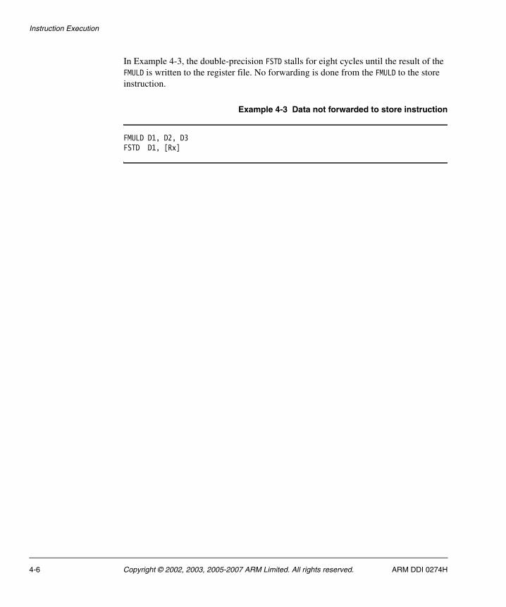
Instruction Execution
In Example 4-3, the double-precision FSTD stalls for eight cycles until the result of the FMULD is written to the register file. No forwarding is done from the FMULD to the store instruction.
Example 4-3 Data not forwarded to store instruction
FMULD D1, D2, D3FSTD D1, [Rx]
4-6 Copyright © 2002, 2003, 2005-2007 ARM Limited. All rights reserved. ARM DDI 0274H

Instruction Execution
4.5 Hazards
The VFP11 coprocessor incorporates full hazard detection with a fully-interlocked pipeline protocol. No compiler scheduling is required to avoid hazard conditions. The source and destination scoreboards process interlocks caused by unavailable source or destination registers or by unavailable data. The scoreboards stall instructions until all data operands and destination registers are available before the instruction is issued to the instruction pipeline.
The determination of hazards and interlock conditions is different in full-compliance mode and RunFast mode. RunFast mode guarantees no bounce conditions and has a less strict hazard detection mechanism, enabling instructions to begin execution earlier than in full-compliance mode.
There are two VFP11 pipeline hazards:
• A data hazard is a combination of instructions that creates the potential for operands to be accessed in the wrong order.
— A Read-After-Write (RAW) data hazard occurs when the pipeline creates the potential for an instruction to read an operand before a prior instruction writes to it. It is a hazard to the intended read-after-write operand access.
— A Write-After-Read (WAR) data hazard occurs when the pipeline creates the potential for an instruction to write to a register before a prior instruction reads it. It is a hazard to the intended write-after-read operand access.
— A Write-After-Write (WAW) data hazard occurs when the pipeline creates the potential for an instruction to write to a register before a prior instruction writes to it. It is a hazard to the intended write-after-write operand access.
• Resource hazard. See Resource hazards on page 4-20.
ARM DDI 0274H Copyright © 2002, 2003, 2005-2007 ARM Limited. All rights reserved. 4-7

Instruction Execution
4.6 Operation of the scoreboards
The VFP11 processor detects all hazard conditions that exist between issued and executing instructions. It uses two scoreboards to ensure that all source and destination registers for an instruction contain valid data and are available for reading or writing:
• The destination scoreboard contains a lock for each destination register for the current operation.
• The source scoreboard contains a lock for each source register for the current operation.
In the Decode stage of the VFP11 pipeline, the VFP11 coprocessor determines which source and destination registers are involved in an operation and generates a lock mask for them. In a short vector operation, the lock mask includes the registers involved in every iteration of the operation. In the Issue stage, the VFP11 coprocessor checks and updates the source and destination scoreboards. If it detects a hazard between the instruction in the Issue stage and a prior instruction, the scoreboards are not updated, and the instruction stalls in the Issue stage.
A VFP11 instruction can begin execution only when its source and destination registers are free of locks. A short vector operation can begin only when the registers for all its iterations are free of locks. When a short vector instruction proceeds in the pipeline beyond the Issue stage, all the registers involved in the operation are locked.
The source scoreboard clears a source register lock in the first Execute 1 stage of the pipeline or in the first Execute 1 stage of the iteration. In store multiple instructions, the source scoreboard clears source register locks in the Execute stage in which the instruction writes the store data to the ARM1136 processor.
The destination scoreboard clears the destination register lock in the cycle before the result data is written back to the register file or is available for forwarding. This cycle is Execute 7 in the FMAC pipeline, and Execute 4 in the DS pipeline. In a load operation, the destination scoreboard normally clears the destination register lock in the Memory 2 stage. If the load is delayed, the destination scoreboard clears the destination register lock in the same cycle as the writeback to the register file.
4.6.1 Scoreboard operation when an instruction bounces
When a bounce occurs in full-compliance mode, support code is called to complete the operation and to deliver the result and the exception status to the user trap handler. The source scoreboard ensures that all source registers for the operation are preserved for the support code. In a short vector operation, this includes the source registers for the
4-8 Copyright © 2002, 2003, 2005-2007 ARM Limited. All rights reserved. ARM DDI 0274H

Instruction Execution
bounced iteration and for any iterations remaining after the bounced iteration. The preserved source registers include the destination register for a multiply and accumulate instruction.
Because RunFast mode guarantees that no bouncing is possible, source registers do not have to be preserved after they are used by the instruction. For all scalar operations and non-multiple store operations, no source registers are locked in RunFast mode. In short vector operations, the length of the vector determines which source registers are locked. When the vector length exceeds four single-precision iterations, the source scoreboard locks the source registers for iterations 5 and above. When the vector length exceeds two double-precision iterations, the source scoreboard locks the source registers for iterations 3 and above.
4.6.2 Single-precision source register locking
In full-compliance mode, the source scoreboard locks all source registers in the Issue stage of the instruction. In RunFast mode, the source scoreboard locks the source registers only for iterations 5, 6, 7, and 8. Table 4-1 summarizes source register locking in single-precision operations.
For the following single-precision short vector instruction, the LEN field contains b100, selecting a vector length of five iterations:
FADDS S8, S16, S24
Table 4-1 Single-precision source register locking
LEN Vector length
Source registers locked in Issue stage
Full-compliance mode RunFast mode
b000 1 Iteration 1 registers -
b001 2 Iteration 1-2 registers -
b010 3 Iteration 1-3 registers -
b011 4 Iteration 1-4 registers -
b100 5 Iteration 1-5 registers Iteration 5 registers
b101 6 Iteration 1-6 registers Iteration 5-6 registers
b110 7 Iteration 1-7 registers Iteration 5-7 registers
b111 8 Iteration 1-8 registers Iteration 5-8 registers
ARM DDI 0274H Copyright © 2002, 2003, 2005-2007 ARM Limited. All rights reserved. 4-9

Instruction Execution
The FADDS instruction performs the following operations:
FADDS S8, S16, S24FADDS S9, S17, S25FADDS S10, S18, S26FADDS S11, S19, S27FADDS S12, S20, S28
In full-compliance mode, the source scoreboard locks S16-S20 and S24-S28 in the Issue stage of the instruction.
In RunFast mode, the source scoreboard locks only the fifth iteration source registers, S20 and S28.
4.6.3 Single-precision source register clearing
In full-compliance mode, the source scoreboard clears the source registers of each iteration in the Execute 1 stage of the iteration. In RunFast mode, it locks the source registers only for iterations 5, 6, 7, and 8, and the source scoreboard begins clearing them in the second Execute 1 cycle of the instruction. Table 4-2 summarizes source register clearing in single-precision operations.
For the following single-precision short vector instruction, the LEN field contains b100, selecting a vector length of five iterations:
FADDS S8, S16, S24
Table 4-2 Single-precision source register clearing
Execute 1 cycle
Source registers cleared in Execute 1 stage of each iteration
Full-compliance mode RunFast mode
1 Iteration 1 registers -
2 Iteration 2 registers Iteration 5 registers
3 Iteration 3 registers Iteration 6 registers
4 Iteration 4 registers Iteration 7 registers
5 Iteration 5 registers Iteration 8 registers
6 Iteration 6 registers -
7 Iteration 7 registers -
8 Iteration 8 registers -
4-10 Copyright © 2002, 2003, 2005-2007 ARM Limited. All rights reserved. ARM DDI 0274H

Instruction Execution
The FADDS instruction performs the following operations:
FADDS S8, S16, S24FADDS S9, S17, S25FADDS S10, S18, S26FADDS S11, S19, S27FADDS S12, S20, S28
In full-compliance mode, the source scoreboard clears the source registers of each iteration in the Execute 1 cycle of the iteration.
In RunFast mode, the source scoreboard locks only the fifth iteration source registers, S20 and S28. It clears S20 and S28 in the second Execute 1 cycle of the instruction.
4.6.4 Double-precision source register locking
In full-compliance mode, the source scoreboard locks all source registers in the Issue stage of the instruction. In RunFast mode, the source scoreboard locks the source registers only for iterations 3 and 4. Table 4-3 summarizes source register locking in double-precision operations.
For the following double-precision, short vector instruction, the LEN field contains b011, selecting a vector length of four iterations:
FADDD D4, D8, D12
The FADDD instruction performs the following operations:
FADDD D4, D8, D12FADDD D5, D9, D13FADDD D6, D10, D14FADDD D7, D11, D15
Table 4-3 Double-precision source register locking
LEN Vector length
Source registers locked in Issue stage
Full-compliance mode RunFast mode
b000 1 Iteration 1 registers -
b001 2 Iteration 1-2 registers -
b010 3 Iteration 1-3 registers Iteration 3 registers
b011 4 Iteration 1-4 registers Iteration 3-4 registers
ARM DDI 0274H Copyright © 2002, 2003, 2005-2007 ARM Limited. All rights reserved. 4-11

Instruction Execution
In full-compliance mode, the source scoreboard locks D8-D11 and D12-D15 in the Issue stage of the instruction.
In RunFast mode, the source scoreboard locks only the third iteration source registers, D10 and D14, and the fourth iteration source registers, D11 and D15.
4.6.5 Double-precision source register clearing
The number of Execute 1 cycles required to clear the source registers of a double-precision instruction depends on the throughput of the instruction, as the following sections show:
• Instructions with one-cycle throughput
• Instructions with two-cycle throughput on page 4-13.
Instructions with one-cycle throughput
In full-compliance mode, the source scoreboard clears the source registers of each iteration in the Execute 1 stage of the iteration. In RunFast mode, only the source registers for iterations 3 and 4 are locked, and the source scoreboard begins clearing them in the first Execute 1 cycle of the instruction. Table 4-4 summarizes source register clearing for double-precision one-cycle instructions such as FADDD and FABSD.
For the following one-cycle, double-precision short vector instruction, the LEN field contains b011, selecting a vector length of four iterations:
FADDD D4, D8, D12
The FADDD performs the following operations:
FADDD D4, D8, D12FADDD D5, D9, D13FADDD D6, D10, D14
Table 4-4 Double-precision source register clearing for one-cycle instructions
Execute 1 cycle
Source registers cleared in Execute 1 stage of each iteration
Full-compliance mode RunFast mode
1 Iteration 1 registers Iteration 3 registers
2 Iteration 2 registers Iteration 4 registers
3 Iteration 3 registers -
4 Iteration 4 registers -
4-12 Copyright © 2002, 2003, 2005-2007 ARM Limited. All rights reserved. ARM DDI 0274H
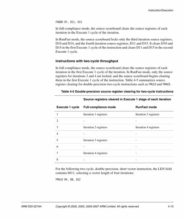
Instruction Execution
FADDD D7, D11, D15
In full-compliance mode, the source scoreboard clears the source registers of each iteration in the Execute 1 cycle of the iteration.
In RunFast mode, the source scoreboard locks only the third iteration source registers, D10 and D14, and the fourth iteration source registers, D11 and D15. It clears D10 and D14 in the first Execute 1 cycle of the instruction and clears D11 and D15 in the second Execute 1 cycle.
Instructions with two-cycle throughput
In full-compliance mode, the source scoreboard clears the source registers of each iteration in the first Execute 1 cycle of the iteration. In RunFast mode, only the source registers for iterations 3 and 4 are locked, and the source scoreboard begins clearing them in the first Execute 1 cycle of the instruction. Table 4-5 summarizes source register clearing for double-precision two-cycle instructions such as FMULD and FMACD.
For the following two-cycle, double-precision, short vector instruction, the LEN field contains b011, selecting a vector length of four iterations:
FMULD D4, D8, D12
Table 4-5 Double-precision source register clearing for two-cycle instructions
Execute 1 cycle
Source registers cleared in Execute 1 stage of each iteration
Full-compliance mode RunFast mode
1 Iteration 1 registers Iteration 3 registers
2 - -
3 Iteration 2 registers Iteration 4 registers
4 - -
5 Iteration 3 registers -
6 - -
7 Iteration 4 registers -
8 - -
ARM DDI 0274H Copyright © 2002, 2003, 2005-2007 ARM Limited. All rights reserved. 4-13

Instruction Execution
The FMULD instruction performs the following operations:
FMULD D4, D8, D12FMULD D5, D9, D13FMULD D6, D10, D14FMULD D7, D11, D15
In full-compliance mode, the source scoreboard clears the source registers of each iteration in the first Execute 1 cycle of the iteration.
In RunFast mode, only the third iteration source registers, D10 and D14, and the fourth iteration source registers, D11 and D15, are locked. The source scoreboard clears D10 and D14 in the first Execute 1 cycle and clears D11 and D15 in the third Execute 1 cycle of the instruction.
4-14 Copyright © 2002, 2003, 2005-2007 ARM Limited. All rights reserved. ARM DDI 0274H

Instruction Execution
4.7 Data hazards in full-compliance mode
The sections that follow give examples of data hazards in full-compliance mode:
• Status register RAW hazard example
• Load multiple-CDP RAW hazard example
• CDP-CDP RAW hazard example on page 4-17
• Load multiple-short vector CDP RAW hazard example on page 4-16
• Short vector CDP-load multiple WAR hazard example on page 4-17.
4.7.1 Status register RAW hazard example
In Example 4-4, the FMSTAT is stalled for four cycles in the Decode stage until the FCMPS updates the condition codes in the FPSCR register. Two cycles later, the FMSTAT writes the condition codes to the ARM1136 processor.
Example 4-4 FCMPS-FMSTAT RAW hazard
FCMPS S1, S2FMSTAT
Table 4-6 shows the VFP11 pipeline stages for Example 4-4.
4.7.2 Load multiple-CDP RAW hazard example
In Example 4-5 on page 4-16, the FADDS is stalled in the Issue stage for six cycles until the FLDM makes its last transfer to the VFP11 coprocessor. S15 is forwarded from the load in cycle 9 to the FADDS.
Table 4-6 FCMPS-FMSTAT RAW hazard
Instruction cycle number
Instruction 1 2 3 4 5 6 7 8 9 10 11
FCMPS D I E1 E2 E3 E4 - - - - -
FMSTAT - D D D D D I E M1 M2 W
ARM DDI 0274H Copyright © 2002, 2003, 2005-2007 ARM Limited. All rights reserved. 4-15
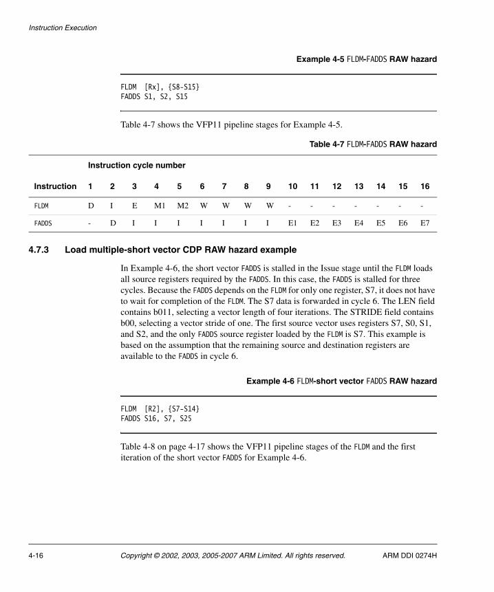
Instruction Execution
Example 4-5 FLDM-FADDS RAW hazard
FLDM [Rx], {S8-S15}FADDS S1, S2, S15
Table 4-7 shows the VFP11 pipeline stages for Example 4-5.
4.7.3 Load multiple-short vector CDP RAW hazard example
In Example 4-6, the short vector FADDS is stalled in the Issue stage until the FLDM loads all source registers required by the FADDS. In this case, the FADDS is stalled for three cycles. Because the FADDS depends on the FLDM for only one register, S7, it does not have to wait for completion of the FLDM. The S7 data is forwarded in cycle 6. The LEN field contains b011, selecting a vector length of four iterations. The STRIDE field contains b00, selecting a vector stride of one. The first source vector uses registers S7, S0, S1, and S2, and the only FADDS source register loaded by the FLDM is S7. This example is based on the assumption that the remaining source and destination registers are available to the FADDS in cycle 6.
Example 4-6 FLDM-short vector FADDS RAW hazard
FLDM [R2], {S7-S14}FADDS S16, S7, S25
Table 4-8 on page 4-17 shows the VFP11 pipeline stages of the FLDM and the first iteration of the short vector FADDS for Example 4-6.
Table 4-7 FLDM-FADDS RAW hazard
Instruction cycle number
Instruction 1 2 3 4 5 6 7 8 9 10 11 12 13 14 15 16
FLDM D I E M1 M2 W W W W - - - - - - -
FADDS - D I I I I I I I E1 E2 E3 E4 E5 E6 E7
4-16 Copyright © 2002, 2003, 2005-2007 ARM Limited. All rights reserved. ARM DDI 0274H

Instruction Execution
4.7.4 CDP-CDP RAW hazard example
In Example 4-7, the FADDS is stalled in the Issue stage for seven cycles until the FMULS data is written and forwarded in cycle 10 to the Issue stage of the FADDS.
Example 4-7 FMULS-FADDS RAW hazard
FMULS S4, S1, S0FADDS S5, S4, S3
Table 4-9 shows the VFP11 pipeline stages of Example 4-7.
4.7.5 Short vector CDP-load multiple WAR hazard example
In Example 4-8 on page 4-18, the load multiple FLDMS creates a WAR hazard to the source registers of the FMULS. The LEN field contains b011, selecting a vector length of four iterations, and the STRIDE field contains b00, selecting a vector stride of one. The VFP11 coprocessor stalls the FLDMS until the FMULS clears the scoreboard locks for all the source registers, S16-S19 and S24-S27.
Table 4-8 FLDM-short vector FADDS RAW hazard
Instruction cycle number
Instruction 1 2 3 4 5 6 7 8 9 10 11 12 13 14 15 16 17
FLDM D I E M1 M2 W W W W - - - - - - - -
FADDS - D I I I I E1 E1 E1 E1 E2 E3 E4 E5 E6 E7 W
Table 4-9 FMULS-FADDS RAW hazard
Instruction cycle number
Instruction 1 2 3 4 5 6 7 8 9 10 11
FMULS D I E1 E2 E3 E4 E5 E6 E7 W -
FADDS - D I I I I I I I I EI
ARM DDI 0274H Copyright © 2002, 2003, 2005-2007 ARM Limited. All rights reserved. 4-17

Instruction Execution
Example 4-8 Short vector FMULS-FLDMS WAR hazard
FMULS S8, S16, S24FLDMS [R2], {S16-S27}
Table 4-10 shows the VFP11 pipeline stages for the first iteration of Example 4-8.
Table 4-10 Short vector FMULS-FLDMS WAR hazard
Instruction cycle number
Instruction 1 2 3 4 5 6 7 8 9 10 11 12 13 14 15 16
FMULS D I E1 E1 E1 E1 E2 E3 E4 E5 E6 E7 W - - -
FLDMS - D I I I I I E M1 M2 W W W W W W
4-18 Copyright © 2002, 2003, 2005-2007 ARM Limited. All rights reserved. ARM DDI 0274H

Instruction Execution
4.8 Data hazards in RunFast mode
In RunFast mode, source registers for the FMAC and FMUL family of instructions are locked:
• when the vector length exceeds four iterations in single-precision instructions
• when the vector length exceeds two iterations in double-precision instructions.
No source registers are locked for scalar instructions.
4.8.1 Short vector CDP-load multiple WAR hazard example
Example 4-9 is the same as Example 4-8 on page 4-18. The LEN field contains b011, selecting a vector length of four iterations, and the STRIDE field contains b00, selecting a vector stride of one. Executing these instructions in RunFast mode reduces the cycle count of the FLDMS by four cycles.
Example 4-9 Short vector FMULS-FLDMS WAR hazard in RunFast mode
FMULS S8, S16, S24FLDMS R2, {S16-S27}
Table 4-11 shows that the VFP11 coprocessor does not stall the FLDMS operation.
Table 4-11 Short vector FMULS-FLDMS WAR hazard in RunFast mode
Instruction cycle number
Instruction 1 2 3 4 5 6 7 8 9 10 11 12 13
FMULS D I E1 E1 E1 E1 E2 E3 E4 E5 E6 E7 W
FLDMS - D I E M1 M2 W W W W W W -
ARM DDI 0274H Copyright © 2002, 2003, 2005-2007 ARM Limited. All rights reserved. 4-19

Instruction Execution
4.9 Resource hazards
A resource hazard exists when the pipeline required for an instruction is unavailable due to a prior instruction. VFP11 resource stalls are possible in the following cases:
• A data transfer operation following an incomplete data transfer operation can cause a resource stall. The ARM1136 processor can stall each data transfer because of unavailable data caused by memory latency or a cache miss, increasing the latency of the data transfer instruction and stalling any following data transfer instructions.
• An arithmetic operation following either a short vector arithmetic operation or a double-precision multiply or multiply and accumulate operation can cause a resource stall. The latency for a double-precision multiply or multiply and accumulate operation is two cycles, causing a single-cycle stall for an arithmetic operation that immediately follows.
• A single-precision divide or square root operation stalls subsequent DS operations for 15 cycles. A double-precision divide or square root operation stalls subsequent DS operations for 29 cycles.
• A short vector divide or square root operation requires the FMAC pipeline for the first cycle of each iteration and stalls any following CDP operation. The following CDP operation stalls until the final iteration of the short vector divide or square root operation completes the Execute 1 stage.
The LS pipeline is separate from the FMAC and DS pipelines. No resource hazards exist between data transfer instructions and arithmetic instructions.
The sections that follow give examples of resource hazards:
• Load multiple-load-CDP resource hazard example
• Load multiple-short vector CDP resource hazard example on page 4-21
• Short vector CDP-CDP resource hazard example on page 4-22.
4.9.1 Load multiple-load-CDP resource hazard example
In Example 4-10 on page 4-21, the FLDM is executing two transfers to the VFP11 coprocessor. The FLDS is stalled behind the FLDM until the FLDM enters the final Execute cycle. The FADDS is stalled for one cycle until the FLDS begins execution.
4-20 Copyright © 2002, 2003, 2005-2007 ARM Limited. All rights reserved. ARM DDI 0274H

Instruction Execution
Example 4-10 FLDM-FLDS-FADDS resource hazard
FLDM [R2], {S8-S10}FLDS [R4], S16 FADDS S2, S3, S4
Table 4-12 shows the pipeline stages for Example 4-10.
4.9.2 Load multiple-short vector CDP resource hazard example
In Example 4-11, no resource hazard exists for the FMULS due to the FLDM in the prior cycle. The FMULS is issued to the VFP11 coprocessor in the cycle following the issue of the FLDM, and executes in parallel with it.
The LEN field contains, b011, selecting a vector length of four iterations. The STRIDE field contains b00, selecting a vector stride of one.
Example 4-11 FLDM-short vector FMULS resource hazard
FLDM [R2], {S8-S10}FMULS S16, S24, S4
Table 4-13 on page 4-22 shows the pipeline stages for Example 4-11.
Table 4-12 FLDM-FLDS-FADDS resource hazard
Instruction cycle number
Instruction 1 2 3 4 5 6 7 8 9 10 11 12 13
FLDM D I E M1 M2 W W - -
FLDS - D D I E M1 M2 W -
FADDS - - - D I E1 E2 E3 E4 E5 E6 E7 W
ARM DDI 0274H Copyright © 2002, 2003, 2005-2007 ARM Limited. All rights reserved. 4-21

Instruction Execution
4.9.3 Short vector CDP-CDP resource hazard example
In Example 4-12, a short vector divide is followed by a FADDS instruction. The short vector divide has b001 in the LEN field, selecting a vector length of two iterations. It requires the Execute 1 stage of the FMAC pipeline for the first cycle of each iteration of the divide, resulting in a stall of the FADDS until the final iteration of the divide completes the first Execute 1 cycle. The divide iterates for 14 cycles in the Execute 1 and Execute 2 stages of the DS pipeline, shown in Table 4-14 as E1. The first and shared Execute 1 cycle for each divide iteration is designated as E1’.
Example 4-12 Short vector FDIVS-FADDS resource hazard
FDIVS S8, S10, S12FADDS S0, S0, S1
Table 4-14 and Table 4-15 on page 4-23 show the pipeline stages for Example 4-12.
Table 4-13 FLDM-short vector FMULS resource hazard
Instruction cycle number
Instruction 1 2 3 4 5 6 7 8 9 10 11 12 13 14
FLDM D I E M1 M2 W W - -
FMULS - D I E1 E1 E1 E1 E2 E3 E4 E5 E6 E7 W
Table 4-14 Short vector FDIVS-FADDS resource hazard, cycles 1 to 22
Instruction cycle number, cycles 1 to 22
Instruction 1 2 3 4 … 16 17 18 19 20 21 22
FDIVS D I E1’ E1 … E1 E1 E1’ E1 E1 E1 E1
FADDS - - D D … D D I E1 E2 E3 E4
4-22 Copyright © 2002, 2003, 2005-2007 ARM Limited. All rights reserved. ARM DDI 0274H

Instruction Execution
Table 4-15 Short vector FDIVS-FADDS resource hazard, cycles 23 to 36
Instruction cycle number, cycles 23 to 36
Instruction 23 24 25 26 … 30 31 32 33 34 35 36
FDIVS E1 E1 E1 E1 … E1 E1 E1 E2 E3 E4 W
FADDS E5 E6 E7 W … - - - - - - -
ARM DDI 0274H Copyright © 2002, 2003, 2005-2007 ARM Limited. All rights reserved. 4-23

Instruction Execution
4.10 Parallel execution
The VFP11 coprocessor can execute in each of the three pipelines independently of the others and without blocking issue or writeback from any pipeline. Separate LS, FMAC, and DS pipelines enable parallel operation of CDP and data transfer instructions. Scheduling instructions to take advantage of the parallelism that occurs when multiple instructions execute in the VFP11 pipelines can result in a significant improvement in program execution time.
A data transfer operation can begin execution if:
• no data hazards exist with any currently executing operations
• the LS pipeline is not currently stalled by the ARM1136 processor or busy with a data transfer multiple.
A CDP can be issued to the FMAC pipeline if:
• No data hazards exist with any currently executing operations
• The FMAC pipeline is available. The pipeline is available if no short vector CDP is executing and no double-precision multiply is in the first cycle of the multiply operation.
• No short vector operation with unissued iterations is currently executing in either the FMAC or DS pipeline.
A divide or square root instruction can be issued to the DS pipeline if:
• No data hazards exist with any currently executing operations.
• The DS pipeline is available. The pipeline is available if no current divide or square root is executing in the DS pipeline E1 stage.
• No short vector operation with unissued iterations is executing in the FMAC pipeline.
Example 4-13 on page 4-25 shows a case of the VFP11 coprocessor executing instructions in parallel in each of the three pipelines:
• a load multiple in the L/S pipeline
• a divide in the DS pipeline
• a short vector add in the FMAC pipeline.
In this example, the LEN field contains b011, selecting a vector length of four iterations, and the STRIDE field contains b00, for a vector stride of one.
4-24 Copyright © 2002, 2003, 2005-2007 ARM Limited. All rights reserved. ARM DDI 0274H

Instruction Execution
Example 4-13 Parallel execution in all three pipelines
FLDM [R4], {S4-S13}FDIVS S0, S1, S2FADDS S16, S20, S24
Table 4-16 shows the pipeline progression of the three instructions.
In Example 4-13, no data hazards exist between any of the three instructions. The load multiple can begin execution immediately, and data is transferred to the register file beginning in cycle 6. Because the destination is in bank 0, the FDIVS is a scalar operation and requires one cycle in the FMAC pipeline E1 stage. If the FDIVS was a short vector operation, the FADDS could not begin execution until the last FDIVS iteration passed the FMAC E1 pipeline stage. The FADDS is a short vector operation and requires the FMAC pipeline E1 stage for cycles 5-8.
Note E1’ is the first cycle in E1 and is in both FMAC and DS blocks. Subsequent E1 cycles represent the iteration cycles and occupy both E1 and E2 stages in the DS block.
Table 4-16 Parallel execution in all three pipelines
Instruction cycle number
Instruction 1 2 3 4 5 6 7 8 9 10 11 12 13 14 15
FLDM D I E M1 M2 W W W W W - - - - -
FDIVS - D I E1’ E1 E1 E1 E1 E1 E1 E1 E1 E1 E1 E1
FADDS - - D I E1 E1 E1 E1 E2 E3 E4 E5 E6 E7 W
ARM DDI 0274H Copyright © 2002, 2003, 2005-2007 ARM Limited. All rights reserved. 4-25

Instruction Execution
4.11 Execution timing
Complex instruction dependencies and memory system interactions make it impossible to describe briefly the exact cycle timing of all instructions in all circumstances. The timing shown in Table 4-17 is accurate in most cases. For precise timing, you must use a cycle-accurate model of the ARM1136JF-S processor.
In Table 4-17, throughput is defined as the cycle after issue in which another instruction can begin execution. Instruction latency is the number of cycles after which the data is available for another operation. Forwarding reduces the latency by one cycle for operations that depend on floating-point data. Table 4-17 shows the throughput and latency for all VFP11 instructions.
Table 4-17 Throughput and latency cycle counts for VFP11 instructions
Instructions
Single-precision Double-precision
Throughput Latency Throughput Latency
FABS, FNEG, FCVT, FCPY 1 4 1 4
FCMP, FCMPE, FCMPZ, FCMPEZ 1 4 1 4
FSITO, FUITO, FTOSI, FTOUI, FTOUIZ, FTOSIZ 1 8 1 8
FADD, FSUB 1 8 1 8
FMUL, FNMUL 1 8 2 9
FMAC, FNMAC, FMSC, FNMSC 1 8 2 9
FDIV, FSQRT 15 19 29 33
FLDa 1 4 1 4
FSTa 1a System- dependent 1 System- dependent
FLDMa Xb Xb + 3 Xb Xb + 3
FSTMa Xb System- dependent Xb System- dependent
FMSTAT 1 2 - -
FMSR, FMSRRc 1 4 - -
FMDHR, FMDHC, FMDRRc - - 1 4
FMRS, FMRRSc 1 2 - -
4-26 Copyright © 2002, 2003, 2005-2007 ARM Limited. All rights reserved. ARM DDI 0274H

Instruction Execution
FMRDH, FMRDL, FMRRDc - - 1 2
FMXRd 1 4 - -
FMRXd 1 2 - -
a. The cycle count for a load instruction is based on load data that is cached and available to the ARM1136 processor from the cache. The cycle count for a store instruction is based on store data that is written to the cache and/or write buffer immediately. When the data is not cached or the write buffer is unavailable, the number of cycles also depends on the memory subsystem.
b. The number of cycles represented by X is (N/2) if N is even or (N/2 + 1) if N is odd. c. FMDRR and FMRRD transfer one double-precision data per transfer. FMSRR and FMRRS transfer two single-precision data per transfer.d. FMXR and FMRX are serializing instructions. The latency depends on the register transferred and the current activity in the VFP11
coprocessor when the instruction is issued.
Table 4-17 Throughput and latency cycle counts for VFP11 instructions (continued)
Instructions
Single-precision Double-precision
Throughput Latency Throughput Latency
ARM DDI 0274H Copyright © 2002, 2003, 2005-2007 ARM Limited. All rights reserved. 4-27

Instruction Execution
4-28 Copyright © 2002, 2003, 2005-2007 ARM Limited. All rights reserved. ARM DDI 0274H

Chapter 5 Exception Handling
This chapter describes VFP11 exception processing. It contains the following sections:
• About exception processing on page 5-2
• Bounced instructions on page 5-3
• Support code on page 5-5
• Exception processing on page 5-8
• Input Subnormal exception on page 5-14
• Invalid Operation exception on page 5-15
• Division by Zero exception on page 5-18
• Overflow exception on page 5-19
• Underflow exception on page 5-21
• Inexact exception on page 5-23
• Input exceptions on page 5-24
• Arithmetic exceptions on page 5-25.
ARM DDI 0274H Copyright © 2002, 2003, 2005-2007 ARM Limited. All rights reserved. 5-1

Exception Handling
5.1 About exception processing
The VFP11 coprocessor handles exceptions imprecisely with respect to both the state of the ARM1136JF-S processor and the state of the VFP11 coprocessor. It detects an exceptional instruction after the instruction passes the point for exception handling in the ARM1136 processor. It then enters the exceptional state and signals the exception by refusing to accept a subsequent VFP instruction. The instruction that triggers exception handling bounces to the ARM1136 processor. The bounced instruction is not necessarily the instruction immediately following the exceptional instruction. Depending on sequence of instructions that follow the exceptional instruction, the bounce can occur several instructions later.
The VFP11 coprocessor can generate exceptions only on arithmetic operations. Data transfer operations between the ARM1136 processor and the VFP11 coprocessor, and instructions that copy data between VFP11 registers, FCPY, FABS, and FNEG, cannot produce exceptions.
In full-compliance mode the VFP11 hardware and support code together process exceptions according to the IEEE 754 standard. VFP11 exception processing includes calling user trap handlers with intermediate operands specified by the IEEE 754 standard. In RunFast mode, the VFP11 coprocessor generates the default, or trap disabled, value when an overflow, invalid operation, division by zero, or inexact condition occurs. RunFast mode does not support user trap handlers.
For descriptions of each of the exception flags and their bounce characteristics, see:
• Input Subnormal exception on page 5-14
• Invalid Operation exception on page 5-15
• Division by Zero exception on page 5-18
• Overflow exception on page 5-19
• Underflow exception on page 5-21
• Inexact exception on page 5-23
• Input exceptions on page 5-24
• Arithmetic exceptions on page 5-25.
5-2 Copyright © 2002, 2003, 2005-2007 ARM Limited. All rights reserved. ARM DDI 0274H

Exception Handling
5.2 Bounced instructions
Normally, the VFP11 hardware executes floating-point instructions completely in hardware. However, the VFP11 coprocessor can, under certain circumstances, refuse to accept a floating-point instruction, causing the ARM Undefined Instruction exception. This is known as bouncing the instruction.
There are three reasons for bouncing an instruction:
• a prior instruction generates a potential or actual floating-point exception that cannot be properly handled by the VFP11 coprocessor, such as a potential underflow when the VFP11 coprocessor is not in flush-to-zero mode
• a prior instruction generates a potential or actual floating-point exception when the corresponding exception enable bit is set to 1 in the FPSCR, such as a square root of a negative value when the IOE bit, FPSCR[8], is set
• the current instruction is Undefined.
When a floating-point exception is detected, the VFP11 hardware sets the EX flag, FPEXC[31], to 1, and loads the FPINST register with a copy of the exceptional instruction. The VFP11 coprocessor is now in the exceptional state. The instruction that bounces as a result of the exceptional state is referred to as the trigger instruction.
See Exception processing on page 5-8.
5.2.1 Potential or actual exception that the VFP11 coprocessor cannot handle
Three exceptional conditions cannot be handled by the VFP11 hardware:
• an operation that might underflow when the VFP11 coprocessor is not in flush-to-zero mode
• an operation involving a subnormal operand when the VFP11 coprocessor is not in flush-to-zero mode
• an operation involving a NaN when the VFP11 coprocessor is not in default NaN mode.
For these conditions the VFP11 coprocessor requires support code to process the operation. See Underflow exception on page 5-21 and Input exceptions on page 5-24.
ARM DDI 0274H Copyright © 2002, 2003, 2005-2007 ARM Limited. All rights reserved. 5-3

Exception Handling
5.2.2 Potential or actual exception with the exception enable bit set
The VFP11 coprocessor evaluates the instruction for exceptions in the E1 and E2 pipeline stages. There is no mechanism to signal exceptions to the ARM1136 processor after the E2 stage. The VFP11 coprocessor enters the exceptional state when it detects that an instruction has a potential to generate a floating-point exception while the corresponding exception enable bit is set to 1. Such an instruction is called a potentially exceptional instruction.
An example of an instruction that generates an actual exception is a division of a normal value by zero when the Division by Zero exception enable bit, FPSCR[9], is set to 1. This mechanism provides support for the IEEE 754 trap mechanism and enables software to halt execution on certain conditions.
The following is an example of an instruction that generates a potential exception. If the overflow exception enable bit, FPSCR[10], is set to 1, and the initial exponent for a multiply operation is the maximum exponent for a normal value in the destination precision, the VFP11 coprocessor bounces the instruction pessimistically. Since the impact on the exponent due to mantissa overflow and rounding is not known in the E1 or E2 stages of the FMAC pipeline, the decision to bounce must be made based on the potential for an exception. Support code performs the multiply operation and determines the exception status. If the multiply operation results in an overflow, the processor jumps to the Overflow user trap handler. If the operation does not result in an overflow, it writes the computed result to the destination, sets the appropriate flags in the FPSCR, and returns to user code.
5-4 Copyright © 2002, 2003, 2005-2007 ARM Limited. All rights reserved. ARM DDI 0274H

Exception Handling
5.3 Support code
The VFP11 coprocessor provides floating-point functionality through a combination of hardware and software support.
When an instruction bounces, software installed on the ARM Undefined Instruction vector determines why the VFP11 coprocessor rejected the instruction and takes appropriate remedial action. This software is called the VFP support code. The support code has two components:
• a library of routines that perform floating-point arithmetic functions
• a set of exception handlers that process exceptional conditions.
See Application Note 98, VFP Support Code for details of support code. Support code is provided with the RealView Compilation Tools, or for the ARM Developer Suite as an add-on downloadable from the ARM web site.
The remedial action is performed as follows:
1. The support code starts by reading the FPEXC register. If the EX flag, FPEXC[31], is set to 1, a potential exception is present. If not, an illegal instruction was detected. See Illegal instructions on page 5-6.
The contents of the FPEXC register must be retained throughout exception processing. Any VFP11 coprocessor activity might change FPEXC register bits from their state at the time of the exception.
2. The support code writes to the FPEXC register to clear the EX flag to 0. Failure to do this can result in an infinite loop of exceptions when the support code next accesses the VFP11 hardware.
3. The support code reads the FPINST register to determine the instruction that caused the potential exception.
4. The support code decodes the instruction in the FPINST register, reads its operands, including implicit information such as the rounding mode and vector length in the FPSCR register, executes the operation, and determines whether a floating-point exception occurred.
5. If no floating-point exception occurred, the support code writes the correct result of the operation and sets the appropriate flags in the FPSCR register.
If one or more floating-point exceptions occurred, but all of them were disabled, the support code determines the correct result of the instruction, writes it to the destination register, and sets the corresponding flags in the FPSCR register.
If one or more floating-point exceptions occurred, and at least one of them was enabled, the support code computes the intermediate result specified by the IEEE 754 standard, if required, and calls the user trap handler for that exception.
ARM DDI 0274H Copyright © 2002, 2003, 2005-2007 ARM Limited. All rights reserved. 5-5
Exception Handling
The user trap handler can provide a result for the instruction and continue program execution, or generate a signal or message to the operating system or the user, or simply terminate the program.
6. If the potentially exceptional instruction specified a short vector operation, the hardware does not execute any vector iterations after the one that encountered the potentially exceptional condition. The support code repeats steps 4 and 5 for any such iterations. See Exception processing for CDP short vector instructions on page 5-9 for more details.
7. If the FP2V flag, FPEXC[28], is set to 1, the FPINST2 register contains another VFP instruction that was issued between the potentially exceptional instruction and the trigger instruction. This instruction is executed by the support code in the same manner as the instruction in the FPINST register. The FP2V flag must be cleared before returning to user code. See Floating Point Instruction Registers, FPINST and FPINST2 on page 3-23 for more information about FPINST2.
8. The support code finishes processing the potentially exceptional instruction and returns to the program containing the trigger instruction. The ARM1136 processor re-fetches the trigger instruction from memory and reissues it to the VFP11 coprocessor. Unless another bounce occurs, the trigger instruction is executed. Returning in this fashion is called retrying the trigger instruction.
The support code can be written to use the VFP11 hardware for its internal calculations, provided that:
• recursive bounces are prevented or handled correctly
• the state of the original program is always restored before returning to it.
Restoring the state of the original program can be difficult if the original program was executing in FIQ mode or in Undefined Instruction mode. It is legitimate for support code to disallow or restrict the use of VFP11 instructions in these two processor modes.
5.3.1 Illegal instructions
If there is not a potential floating-point exception from an earlier instruction, the current instruction can still be bounced if it is architecturally Undefined in some way. When this happens, the EX flag, FPEXC[31], is not set to 1. The instruction that caused the bounce is contained in the memory word pointed to by r14_undef – 4.
It is possible that both conditions for an instruction to be bounced occur simultaneously. This happens when an illegal instruction is encountered and there is also a potential floating-point exception from an earlier instruction. When this happens, the EX flag is set to 1, and the support code processes the potential exception in the earlier instruction. If and when it returns, it causes the illegal instruction to be retried. That instruction is then handled as described in this section.
5-6 Copyright © 2002, 2003, 2005-2007 ARM Limited. All rights reserved. ARM DDI 0274H

Exception Handling
The following instruction types are architecturally Undefined. For more information see the ARM Architecture Reference Manual:
• instructions with opcode bit combinations defined as Reserved in the architecture specification
• load or store instructions with Undefined P, W, and U bit combinations
• FMRX and FMXR instructions to or from a control register that is not defined
• User mode FMRX and FMXR instructions to or from a control register that can be accessed only in a privileged mode
• double precision operations with odd register numbers.
Certain instruction types do not have architecturally-defined behavior and are Unpredictable:
• load or store multiple instructions with a transfer count of zero or greater than 32, and any combination of initial register and transfer count such that an attempt is made to transfer a register beyond S31 for single-precision transfers, or D15 for double-precision transfers
• a short vector instruction with a combination of precision, length, and stride that causes the vector to wrap around and make more than one access to the same register
• a short vector instruction with overlapping source and destination register addresses that are not exactly the same.
ARM DDI 0274H Copyright © 2002, 2003, 2005-2007 ARM Limited. All rights reserved. 5-7

Exception Handling
5.4 Exception processing
The interface between the ARM1136JF-S processor and the VFP11 coprocessor specifies that an exceptional instruction that bounces to support code must signal on a subsequent coprocessor instruction. This is known as imprecise exception handling. It means that when the exception is processed, the VFP11 and ARM1136 user states might be different from their states when the exceptional instruction executed. Parallel execution of VFP11 CDP instructions and data transfer instructions means that the VFP11 and ARM1136 register files and memory might be modified outside the program order.
5.4.1 Determination of the trigger instruction
The issue timing of VFP11 instructions affects the determination of the trigger instruction. The last iteration of a short vector CDP can be followed in the next cycle by a second CDP instruction. If there is no hazard, the VFP11 coprocessor accepts the second CDP instruction before the exception status of the last iteration of the short vector CDP is known. The second CDP instruction is said to be in the pretrigger slot and is retained in the FPINST2 register for the support code.
The following rules determine which instruction is the trigger instruction:
• The first nonserializing instruction after the exceptional condition has been detected is a trigger instruction.
• An instruction that accesses the FPSCR register in any processor mode is a trigger instruction.
• An instruction that accesses the FPEXC, FPINST, or FPINST2 register in a privileged mode is not a trigger instruction.
• An instruction that accesses the FPSID register in any mode is not a trigger instruction.
• A data processing instruction that reaches the LS pipeline Execute stage or a CDP instruction that reaches the FMAC or DS pipeline E1 stage is not the trigger instruction. There can be several of these if the exceptional instruction is a sufficiently long short vector instruction, and the exception is detected on a later iteration.
5-8 Copyright © 2002, 2003, 2005-2007 ARM Limited. All rights reserved. ARM DDI 0274H

Exception Handling
5.4.2 Exception processing for CDP scalar instructions
When the VFP11 coprocessor detects an exceptional scalar CDP instruction, it loads the FPINST register with the instruction word for the exceptional instruction and flags the condition in the FPEXC register. It blocks the exceptional instruction from further execution and completes any instructions currently executing in the FMAC and DS pipelines.
It then examines the pipeline for a trigger instruction:
• If there is a VFP CDP instruction or a load or store instruction in the VFP11 Issue stage, this is the trigger instruction and it is bounced in the cycle after the exception is detected.
• If there is no VFP instruction in the VFP11 Issue stage, the VFP11 coprocessor waits until one is issued. The next VFP instruction is the trigger instruction and is bounced.
When the ARM1136 processor returns from exception processing, it retries the trigger instruction.
5.4.3 Exception processing for CDP short vector instructions
For short vector instructions, any iteration might be exceptional. If an exceptional condition is detected for a vector iteration, the vector iterations issued before the exceptional iteration can complete and retire.
When a short vector iteration is found to be potentially exceptional, the following operations occur:
1. The EX flag, FPEXC[31], is set to 1.
2. The source and destination register addresses are modified in the instruction word to point to the source and destination registers of the potentially exceptional iteration.
3. The FPINST register is loaded with the operation instruction word.
4. The VECITR field, FPEXC[10:8], is written with the number of iterations remaining after the potentially exceptional iteration.
5. The exceptional condition flags are set to 1 in the FPEXC.
ARM DDI 0274H Copyright © 2002, 2003, 2005-2007 ARM Limited. All rights reserved. 5-9

Exception Handling
5.4.4 Examples of exception detection for vector instructions
In Example 5-1, the FMULD instruction is a short vector operation with b011 in the LEN field for a length of four iterations and b00 in the STRIDE field for a vector stride of one. A potential Underflow exception is detected on the third iteration.
Example 5-1 Exceptional short vector FMULD followed by load/store instructions
FMULD D8, D12, D8 ; Short vector double-precision multiply of length 4FLDD D0, [R5] ; Load of 1 double-precision registerFSTMS R3, {S2-S9} ; Store multiple of 8 single-precision registersFLDS S8, [R9] ; Load of 1 single-precision register
A double-precision multiply requires two cycles in the Execute 2 stage. The exception on the third iteration is detected in cycle 8. Before the FMULD exception is detected, the FLDD enters the Decode stage in cycle 2, and the FSTMS enters the Decode stage in cycle 3. The FLDD and the FSTMS complete execution and retire. The FLDS stalls in the Decode stage due to a resource conflict with the FSTMS and is the trigger instruction. It is bounced in cycle 9 and can be retried after exception processing. FPINST2 is invalid, and the FP2V flag, FPEXC[28], is not set to 1.
Table 5-1 shows the pipeline stages for Example 5-1.
Table 5-1 Exceptional short vector FMULD followed by load/store instructions
Instruction cycle number
Instruction 1 2 3 4 5 6 7 8 9 10 11 12 13 14 15 16
FMULD D8, D12, D8 D I E1 E2 E1 E2 E1 E2 - - - - - - - -
FLDD D0, [R5] - D I E M1 M2 W - - - - - - - - -
FSTMS R3, {S2-S9} - - D I E M1 M2 W W W W - - - - -
FLDS S8, [R9] - - - D D D D I * - - - - - - -
5-10 Copyright © 2002, 2003, 2005-2007 ARM Limited. All rights reserved. ARM DDI 0274H

Exception Handling
After exception processing begins, the FPEXC register fields contain the following:
EX 1 The VFP11 coprocessor is in the exceptional state.EN 1FP2V 0 FPINST2 does not contain a valid instruction.VECITR 000 One iteration remains after the exceptional iteration.INV 0UFC 1 Exception detected is a potential underflow.OFC 0IOC 0
The FPINST register contains the FMULD instruction with the following fields modified to reflect the register address of the third iteration.
Fd/D 1010/0 Destination of the third exceptional iteration is D10.Fm/M 1010/0 Fm source of the third exceptional iteration is D10.Fn/N 1110/0 Fn source of the third exceptional iteration is D14.
The FPINST2 register contains invalid data.
In Example 5-2, the first FADDS is a short vector operation with b001 in the LEN field for a vector length of two iterations and b00 in the STRIDE field for a vector stride of one. A potential Invalid Operation exception is detected in the second iteration. The second FADDS progresses to the Execute 1 stage and is captured in the FPINST2 register with the condition field changed to AL, the FP2V flag set to 1, and is not the trigger instruction. The FMULS is the trigger instruction and bounces in cycle 6. It can be retried after exception processing.
Example 5-2 Exceptional short-vector FADDS with a FADDS in the pretrigger slot
FADDS S24, S26, S28 ; Vector single-precision add of length 2FADDS S3, S4, S5 ; Scalar single-precision addFMULS S12, S16, S16 ; Short vector single-precision multiply
Table 5-2 on page 5-12 shows the pipeline stages for Example 5-2.
ARM DDI 0274H Copyright © 2002, 2003, 2005-2007 ARM Limited. All rights reserved. 5-11

Exception Handling
After exception processing begins, the FPEXC register fields contains the following:
EX 1 The VFP11 coprocessor is in the exceptional state.EN 1FP2V 1 FPINST2 contains a valid instruction.VECITR 111 No iterations remaining after exceptional iteration.INV 0UFC 0OFC 0IOC 1 Exception detected is a potential invalid operation.
The FPINST register contains the FADDS instruction with the following fields modified to reflect the register address of the second iteration:
Fd/D 1100/1 Destination is of the second exceptional iteration is S25.Fn/N 1101/1 Fn source is of the second exceptional iteration is S27.Fm/M 1110/1 Fm source is of the second exceptional iteration is S29.
The FPINST2 register contains the instruction word for the second FADDS with the condition field changed to AL.
In Example 5-3, FADDD is a short vector instruction with b011 in the LEN field for a vector length of four iterations and b00 in the STRIDE field for a vector stride of one. It has a potential Overflow exception in the first iteration, detected in cycle 4. The following FMACS is stalled in the Decode stage. The FMACS is the trigger instruction and can be retried after exception processing. FPINST2 is invalid and the FP2V flag is not set.
Example 5-3 Exceptional short vector FADDD with an FMACS trigger instruction
FADDD D4, D4, D12 ; Short vector double-precision add of length 4FMACS S0, S3, S2 ; Scalar single-precision mac
Table 5-2 Exceptional short vector FADDS with a FADDS in the pretrigger slot
Instruction cycle number
Instruction 1 2 3 4 5 6 7 8 9 10 11 12 13 14 15 16
FADDS S24, S26, S28 D I E1 E1 E2 - - - - - - - - - - -
FADDS S3, S4, S5 - D D I E1 - - - - - - - - - - -
FMULS S12, S16, S16 - - - D I * - - - - - - - - - -
5-12 Copyright © 2002, 2003, 2005-2007 ARM Limited. All rights reserved. ARM DDI 0274H

Exception Handling
Table 5-3 shows the pipeline stages for Example 5-3 on page 5-12.
After exception processing begins, the FPEXC register fields contain the following:
EX 1 The VFP11 coprocessor is in the exceptional state.EN 1FP2V 0 FPINST2 does not contain a valid instruction.VECITR 010 Three iterations remain.INV 0UFC 0OFC 1 Exception detected is a potential overflow.IOC 0
The FPINST register contains the FADDD instruction with the following fields modified to reflect the register address of the first iteration:
Fd/D 0100/0 Destination of exceptional iteration is D4.Fn/N 0100/0 Fn source of the first exceptional iteration is D4.Fm/M 1100/0 Fm source of the first exceptional iteration is D12.
FPINST2 contains invalid data.
Table 5-3 Exceptional short vector FADDD with an FMACS trigger instruction
Instruction cycle number
Instruction 1 2 3 4 5 6 7 8 9 10 11 12 13 14 15 16
FADDD D4, D4, D12 D I E1 E2 - - - - - - - - - - - -
FMACS S0, S3, S2 - D D I * - - - - - - - -
ARM DDI 0274H Copyright © 2002, 2003, 2005-2007 ARM Limited. All rights reserved. 5-13

Exception Handling
5.5 Input Subnormal exception
The IDC flag, FPSCR[7], is set to 1 whenever a floating-point operand is subnormal. The behavior of the VFP11 coprocessor with a subnormal input operand is a function of the FZ bit, FPSCR[24]. If FZ is not set to 1, the VFP11 coprocessor bounces on the presence of a subnormal input. If FZ is set to 1, the IDE bit, FPSCR[15], determines whether a bounce occurs.
5.5.1 Exception enabled
Setting the IDE bit to 1 enables Input Subnormal exceptions. On an Input Subnormal exception, the coprocessor sets the following flags to 1:
• the EX flag, FPEXC[31]
• the IDC flag, FPSCR[7].
It then calls the Input Subnormal user trap handler. The source and destination registers for the instruction are unchanged in the VFP11 register file.
5.5.2 Exception disabled
Clearing the IDE bit to 0 disables Input Subnormal exceptions. In flush-to-zero mode, the result of the operation, with the subnormal input replaced with a positive zero, is completed and written to the register file. Any appropriate flags in the FPSCR register are set.
5-14 Copyright © 2002, 2003, 2005-2007 ARM Limited. All rights reserved. ARM DDI 0274H

Exception Handling
5.6 Invalid Operation exception
An operation is invalid if the result cannot be represented, or if the result is not defined.
Table 5-4 shows the operand combinations that produce Invalid Operation exceptions. In addition to the conditions in Table 5-4, any CDP instruction other than FCPY, FNEG, or FABS causes an Invalid Operation exception if one or more of its operands is an SNaN. For more information see Table 3-1 on page 3-5.
Table 5-4 Possible Invalid Operation exceptions
Instruction Invalid Operation exceptions
FADD (+infinity) + (–infinity) or (–infinity) + (+infinity).
FSUB (+infinity) – (+infinity) or (–infinity) – (–infinity).
FCMPE, FCMPEZ Any NaN operand
FMUL, FNMUL Zero × ±infinity or ±infinity × zero.a
FDIV Zero/zero or infinity/infinity.a
FMAC, FNMAC Any condition that can cause an Invalid Operation exception for FMUL or FADD can cause an Invalid Operation exception for FMAC and FNMAC. The product generated by the FMAC or FNMAC multiply operation is considered in the detection of the Invalid Operation exception for the subsequent sum operation.
FMSC, FNMSC Any of the conditions that can cause an Invalid Operation exception for FMUL or FSUB can cause an Invalid Operation exception for FMSC and FNMSC. The product generated by the FMSC or FNMSC multiply operation is considered in the detection of the Invalid Operation exception for the subsequent difference operation.
FSQRT Source is less than 0.
FTOUI Rounded result would lie outside the range 0 ≤ result < 232.
FTOSI Rounded result would lie outside the range –231 ≤ result < 231.
a. In flush-to-zero mode, a subnormal input is treated as a positive zero for detecting an Invalid Operation exception.
ARM DDI 0274H Copyright © 2002, 2003, 2005-2007 ARM Limited. All rights reserved. 5-15

Exception Handling
5.6.1 Exception enabled
Setting the IOE bit, FPSCR[8], to 1 enables Invalid Operation exceptions.
The VFP11 coprocessor causes a bounce to support code for all the invalid operation conditions listed in Table 5-4 on page 5-15. Any arithmetic operation involving an SNaN also causes a bounce to support code. The VFP11 coprocessor detects most Invalid Operations exceptions conclusively but some are detected based on the possibility of an invalid operation. The potentially invalid operations are:
• FTOUI with a negative input. A small negative input might round to a zero, which is not an invalid condition.
• A float-to-integer conversion with a maximum exponent for the destination integer and any rounding mode other than round-towards-zero. The impact of rounding is unknown in the Execute 1 stage.
• An FMAC family operation with an infinity in the A operand and a potential product overflow when an infinity with the sign of the product would result in an invalid condition.
When the VFP11 coprocessor detects a potentially invalid condition, the EX flag, FPEXC[31], and the IOC flag, FPEXC[0], are set to 1. The IOC flag in the FPSCR register, FPSCR[0], is not set to 1 by the hardware and must be set to 1 by the support code before it calls the Invalid Operation user trap handler.
The support code determines the exception status of all bounced instructions. If an invalid condition exists, the support code must call the Invalid Operation user trap handler. The source and destination registers for the instruction are valid in the VFP11 register file.
5.6.2 Exception disabled
If the IOE bit is not set to 1, the VFP11 coprocessor writes a default NaN into the destination register for all operations except integer conversion operations.
Conversion of a floating-point value that is outside the range of the destination integer is an invalid condition rather than an overflow condition. When an invalid condition exists for a float-to-integer conversion, the VFP11 coprocessor delivers a default result to the destination register and sets the IOC flag, FPSCR[0], to 1. Table 5-5 on page 5-17 shows the default results for input values after rounding.
If the VFP11 coprocessor is not in default NaN mode, an arithmetic instruction with an SNaN operand sets the IOC flag to 1 and causes a bounce to support code.
5-16 Copyright © 2002, 2003, 2005-2007 ARM Limited. All rights reserved. ARM DDI 0274H

Exception Handling
Note A negative input to an unsigned conversion that does not round to a true zero in the conversion process sets the IOC flag, FPEXC[0], to 1.
Table 5-5 Default results for invalid conversion inputs
FTOUIS and FTOUID FTOSIS and FTOSID
Input value after rounding Result FPSCR IOC flag set? Result FPSCR IOC flag set?
x 232 0xFFFFFFFF Yes 0x7FFFFFFF Yes
231 ≤ x < 232 Integer No 0x7FFFFFFF Yes
0 ≤ x < 231 Integer No Integer No
0 ≥ x ≥ –231 0x00000000 Yes Integer No
x < –231 0x00000000 Yes 0x80000000 Yes
NaN 0x00000000 Yes 0x00000000 Yes
+infinity 0xFFFFFFFF Yes 0x7FFFFFFF Yes
–infinity 0x00000000 Yes 0x80000000 Yes
ARM DDI 0274H Copyright © 2002, 2003, 2005-2007 ARM Limited. All rights reserved. 5-17

Exception Handling
5.7 Division by Zero exception
The Division by Zero exception is generated for a division by zero of a normal or subnormal value. In flush-to-zero mode, a subnormal input is treated as a positive zero for detection of a division by zero. What happens depends on whether or not the Invalid Operation exception is enabled.
5.7.1 Exception enabled
If the DZE bit, FPSCR[9], is set to 1, the Division by Zero user trap handler is called. The source and destination registers for the instruction are unchanged in the VFP11 register file.
5.7.2 Exception disabled
Clearing the DZE bit to 0 disables Division by Zero exceptions. A correctly signed infinity is written to the destination register, and the DZC flag, FPSCR[1], is set to 1.
5-18 Copyright © 2002, 2003, 2005-2007 ARM Limited. All rights reserved. ARM DDI 0274H

Exception Handling
5.8 Overflow exception
When the OFE bit, FPSCR[10], is set to 1, the hardware detects overflow pessimistically based on the preliminary calculation of the final exponent value. If the OFE bit is not set to 1, the hardware detects overflow conclusively.
5.8.1 Exception enabled
Setting the OFE bit to 1 enables overflow exceptions. The VFP11 coprocessor detects most overflow conditions conclusively, but it detects some based on the possibility of overflow. The initial computation of the result exponent might be the maximum exponent or one less than the maximum exponent of the destination precision. Then the possibility of overflow due to significand overflow or rounding exists, but cannot be known in the first Execute stage. The VFP11 coprocessor bounces such cases and uses the support code to determine the exceptional status of the operation. If there is no overflow, the support code writes the computed result to the destination register and does not set the OFC flag, FPSCR[2], to 1. If there is an overflow, the support code writes the intermediate result to the destination register, sets OFC to 1, and calls the Overflow user trap handler. The support code sets the IXC flag, FPSCR[4], to the appropriate value. When the VFP11 coprocessor detects a potential overflow condition, it sets the EX flag, FPEXC[31], and the OFC flag, FPEXC[2], to 1. The OFC flag in the FPSCR register, FPSCR[2], is not set to 1 by the hardware and must be set to 1 by the support code before it calls the user trap handler. The source and destination registers for the instruction are unchanged in the VFP11 register file. See Arithmetic exceptions on page 5-25 for the conditions that cause an overflow bounce.
5.8.2 Exception disabled
Clearing the OFE bit to 0 disables overflow exceptions. A correctly signed infinity or the largest signed finite number for the destination precision is written to the destination register as Table 5-6 on page 5-20 shows. The coprocessor sets the OFC and IXC flags, FPSCR[2] and FPSCR[4], to 1.
ARM DDI 0274H Copyright © 2002, 2003, 2005-2007 ARM Limited. All rights reserved. 5-19

Exception Handling
Table 5-6 Rounding mode overflow results
Rounding mode Result
Round to nearest Infinity, with the sign of the intermediate result.
Round towards zero Largest magnitude value for the destination size, with the sign of the intermediate result.
Round towards plus infinity
Positive infinity if positive overflow. Largest negative value for the destination size if negative overflow.
Round towards minus infinity
Largest positive value for the destination size if positive overflow. Negative infinity if negative overflow.
5-20 Copyright © 2002, 2003, 2005-2007 ARM Limited. All rights reserved. ARM DDI 0274H

Exception Handling
5.9 Underflow exception
If the coprocessor is not in RunFast mode, it detects Underflow pessimistically. If the support code confirms the potential underflow for an operation with a floating-point result, it generates an underflow exception. How this is confirmed depends on whether the VFP11 coprocessor is in flush-to-zero mode.
If the FZ bit is set to 1, all underflowing results are forced to a positive signed zero and written to the destination register. The UFC flag is set to 1 in the FPSCR. No trap is taken. If the Underflow exception enable bit is set to 1, it is ignored.
If the FZ bit is not set to 1 what happens next depends on whether the Underflow exception is enabled.
5.9.1 Exception enabled
Setting the UFE bit, FPSCR[11] to 1, enables Underflow exceptions. The VFP11 coprocessor detects most underflow conditions conclusively, but it detects some based on the possibility of an underflow. The initial computation of the result exponent might be below a threshold for the destination precision. In this case, the possibility of underflow due to massive cancellation exists, but cannot be known in the first Execute stage. The VFP11 coprocessor bounces such cases and uses the support code to determine the exceptional status of the operation. Underflow is confirmed if the result of the operation after rounding is less in magnitude than the smallest normalized number in the destination format. If there is no underflow, either catastrophic or to a subnormal result, the support code writes the computed result to the destination register and returns without setting the UFC flag, FPSCR[3], to 1. If there is underflow, regardless of any accuracy loss, the support code writes the intermediate result to the destination register, sets UFC to 1, and calls the Underflow user trap handler. The support code sets s the IXC flag, FPSCR[4], to the appropriate value.
When the VFP11 coprocessor detects a potential underflow condition, it sets the EX flag, FPEXC[31], and the UFC flag, FPEXC[3], to 1. The UFC flag in the FPSCR register is not set to 1 by the hardware and must be set by the support code before it calls the user trap handler. The source and destination registers for the instruction are valid in the VFP11 register file. See section Arithmetic exceptions on page 5-25 for the conditions that cause an underflow bounce.
ARM DDI 0274H Copyright © 2002, 2003, 2005-2007 ARM Limited. All rights reserved. 5-21

Exception Handling
5.9.2 Exception disabled
Clearing the UFE bit, FPSCR[11], to 0 disables Underflow exceptions. When the FZ bit, FPSCR[24], is not set to 1, the VFP11 coprocessor bounces on potential underflow cases using the mechanism described in Exception enabled on page 5-21. The correct result is written to the destination register, setting the appropriate exception flags.
When the FZ bit is set to 1, the VFP11 coprocessor makes the determination of underflow before rounding and flushes any result that underflows. A result that underflows returns a positive zero to the destination register and sets the UFC flag, FPSCR[3] to 1.
Note The determination of an underflow condition in flush-to-zero mode is made before rounding rather than after. This means that the VFP11 coprocessor might not return the minimum normal value when rounding would have produced it. Instead, it flushes to zero an intermediate value with the minimum exponent for the destination precision, a fraction of all ones, and a round increment. If the intermediate value was the minimum normal value before the underflow condition test is made, it is not flushed to zero.
5-22 Copyright © 2002, 2003, 2005-2007 ARM Limited. All rights reserved. ARM DDI 0274H

Exception Handling
5.10 Inexact exception
The result of an arithmetic operation on two floating-point values can have more significant bits than the destination register can contain. When this happens, the result is rounded to a value that the destination register can hold and is said to be inexact.
The Inexact exception occurs whenever:
• a result is not equal to the computed result before rounding
• an untrapped Overflow exception occurs
• an untrapped Underflow exception occurs, and there is loss of accuracy.
Note The Inexact exception occurs frequently in normal floating-point calculations and does not indicate a significant numerical error except in some specialized applications. Enabling the Inexact exception by setting the IXE bit, FPSCR[12], to 1 can significantly reduce the performance of the VFP11 coprocessor.
The VFP11 coprocessor handles the Inexact exception differently from the other floating-point exceptions. It has no mechanism for reporting inexact results to the software, but can handle the exception without software intervention as long as the IXE bit, FPSCR[12], is cleared to 0, disabling Inexact exceptions.
5.10.1 Exception enabled
If the IXE bit, FPSCR[12], is set to 1, all CDP instructions are bounced to the support code without any attempt to perform the calculation. The support code must then perform the calculation, determining if any exceptions take place, and handling them appropriately. If it detects an Inexact exception, it calls the Inexact user trap handler.
Note If an Overflow or Underflow exception is also detected, it takes priority over the Inexact exception.
5.10.2 Exception disabled
If the IXE bit, FPSCR[12], is not set to 1, the VFP11 coprocessor writes the result to the destination register and sets the IXC flag, FPSCR[4], to 1.
ARM DDI 0274H Copyright © 2002, 2003, 2005-2007 ARM Limited. All rights reserved. 5-23

Exception Handling
5.11 Input exceptions
The VFP11 hardware processes most input operands without support code assistance. However, the hardware is incapable of processing some operands and bounces the instruction to support code for processing. An arithmetic operation bounces with an Input exception when it has either of the following:
• a NaN operand or operands, and default NaN mode is not enabled
• a subnormal operand or operands, and flush-to-zero mode is not enabled.
Note In default NaN mode, an SNaN input to an arithmetic operation causes an Invalid Operation exception. When the IOE bit, FPSCR[8], is set to 1, the instruction bounces to the Invalid Operation user trap handler. When the IOE bit is set to 0, and the VFP11 coprocessor is not in default NaN mode, the instruction bounces to the support code.
5-24 Copyright © 2002, 2003, 2005-2007 ARM Limited. All rights reserved. ARM DDI 0274H

Exception Handling
5.12 Arithmetic exceptions
This section describes the conditions under which the VFP11 coprocessor bounces an arithmetic instruction based on the potential for an exception. The support code must determine the actual exception status of the instruction. The support code must return either the result and appropriate exception status bits, or the intermediate result and a call to a user trap handler.
The following sections describe the circumstances in which arithmetic exceptions occur:
• FADD and FSUB
• FCMP, FCMPZ, FCMPE, and FCMPEZ on page 5-27
• FMUL and FNMUL on page 5-27
• FMAC, FMSC, FNMAC, and FNMSC on page 5-29
• FDIV on page 5-29
• FSQRT on page 5-30
• FCPY, FABS, and FNEG on page 5-30
• FCVTDS and FCVTSD on page 5-31
• FUITO and FSITO on page 5-31
• FTOUI, FTOUIZ, FTOSI, and FTOSIZ on page 5-31.
5.12.1 FADD and FSUB
In an addition or subtraction, the exponent is initially the larger of the two input exponents. For clarity, we define the operation as a Like-Signed Addition (LSA) or an Unlike-Signed Addition (USA). Table 5-7 specifies how this distinction is made. In the table, + indicates a positive operand, and – indicates a negative operand.
Table 5-7 LSA and USA determination
Instruction Operand A sign Operand B sign Operation type
FADD + + LSA
+ – USA
– + USA
– – LSA
ARM DDI 0274H Copyright © 2002, 2003, 2005-2007 ARM Limited. All rights reserved. 5-25

Exception Handling
Because it is possible for an LSA operation to cause the exponent to be incremented if the significand overflows, overflow bounce ranges for an LSA are more pessimistic than they are for a USA. The LSA ranges are made slightly more pessimistic to incorporate FMAC instructions (see FMAC, FMSC, FNMAC, and FNMSC on page 5-29).
Underflow bounce ranges for a USA are more pessimistic than they are for an LSA. This is to accommodate a massive cancellation in which the result exponent is smaller than the larger operand exponent by as much as the length of the significand. The overflow range for a USA is slightly pessimistic, to reduce the number of logic terms, and therefore it is set to the LSA overflow range. Table 5-8 shows the USA and LSA values and conditions. The exponent values in Table 5-8 are in biased format.
FSUB + + USA
+ – LSA
– + LSA
– – USA
Table 5-7 LSA and USA determination (continued)
Instruction Operand A sign Operand B sign Operation type
Table 5-8 FADD family bounce thresholds
Initial result exponent value
Float value
Condition when not in flush-to-zero mode
DPa SPb SP DP
>0x7FF - DP overflow - Bounce
0x7FF - DP overflow, NaN, or infinity
- Bounce
0x7FE - DP overflow - Bounce
0x7FD - DP overflow - Bounce
0x7FC - DP normal - Normal
>0x47F >0xFF SP overflow Bounce Normal
0x47F 0xFF SP NaN or infinity Bounce Normal
0x47E 0xFE SP overflow Bounce Normal
0x47D 0xFD SP overflow Bounce Normal
5-26 Copyright © 2002, 2003, 2005-2007 ARM Limited. All rights reserved. ARM DDI 0274H

Exception Handling
5.12.2 FCMP, FCMPZ, FCMPE, and FCMPEZ
Compare operations do not generate potential exceptions.
5.12.3 FMUL and FNMUL
Detection of a potential exception is based on the initial product exponent, which is the sum of the multiplicand and multiplier exponents. Table 5-9 on page 5-28 shows the result for specific values of the initial product exponent. The exponent values in Table 5-9 on page 5-28 are in biased format. The exponent can be incremented by a
0x47C 0xFC SP normal Normal Normal
0x3FF 0x7F e = 0 bias value Normal Normal
0x3A0 0x20 SP normal (LSA) Minimum (USA) Normal
0x39F 0x1F SP underflow (USA) Bounce (USA) or normal (LSA) Normal
0x381 0x01 SP normal (LSA) MIN (LSA) Normal
0x380 0x00 SP subnormal Bounce Normal
<0x380 <0x00 SP underflow Bounce Normal
0x040 - DP normal (USA) - Normal (LSA) or minimum (USA)
0x03F - DP underflow (USA) - Normal (LSA) or bounce (USA)
0x001 - DP normal (LSA) - Minimum (LSA) or bounce (USA)
0x000 - DP subnormal - Bounce
<0x000 - DP underflow - Bounce
a. DP = double-precision.b. SP = single-precision.
Table 5-8 FADD family bounce thresholds (continued)
Initial result exponent value
Float value
Condition when not in flush-to-zero mode
DPa SPb SP DP
ARM DDI 0274H Copyright © 2002, 2003, 2005-2007 ARM Limited. All rights reserved. 5-27

Exception Handling
significand overflow condition, which is the cause for the additional bounce values near the real overflow threshold. The one additional value in the bounce range makes the FMUL and FNMUL overflow detection ranges identical to those in Table 5-8 on page 5-26.
Table 5-9 FMUL family bounce thresholds
Initial product exponent value
Float value
Condition in full-compliance mode
DPa SPb SP DP
>0x7FF - DP overflow - Bounce
0x7FF - DP NaN or infinity - Bounce
0x7FE - DP maximum normal - Bounce
0x7FD - DP normal - Bounce
0x7FC - DP normal - Normal
>0x47F >0xFF SP overflow Bounce Normal
0x47F 0xFF SP NaN or infinity Bounce Normal
0x47E 0xFE SP maximum normal Bounce Normal
0x47D 0xFD SP normal Bounce Normal
0x47C 0xFC SP normal Normal Normal
0x3FF 0x7F e = 0 bias value Normal Normal
0x381 0x01 SP normal Normal Normal
0x380 0x00 SP subnormal Bounce Normal
<0x380 <0x00 SP underflow Bounce Normal
0x001 - DP normal - Normal
0x000 - DP subnormal - Bounce
<0x000 - DP underflow - Bounce
a. DP = double-precision.b. SP = single-precision.
5-28 Copyright © 2002, 2003, 2005-2007 ARM Limited. All rights reserved. ARM DDI 0274H

Exception Handling
5.12.4 FMAC, FMSC, FNMAC, and FNMSC
The FMAC family of operations adds to the potential overflow range by generating significand values from zero up to but not including four. In this case it is possible for the final exponent to require incrementing by two to normalize the significand.
The bounce thresholds for the FADD family in Table 5-8 on page 5-26 and for the FMUL family in Table 5-9 on page 5-28 incorporate this additional factor. Those ranges are used to detect potential exceptions for the FMAC family.
5.12.5 FDIV
The thresholds for divide are simple and based only on the difference of the exponents of the dividend and the divisor. It is not possible in a divide operation for the significand to overflow and cause an increment of the exponent. However, it is possible for the significand to require a single bit left shift and the exponent to be decremented for normalization. To reduce logic complexity, the overflow ranges are the same as those of the LSA operations in FADD and FSUB on page 5-25. The underflow ranges include the minimum normal exponent, 0x01 for single-precision and 0x001 for double-precision. Table 5-10 shows the FDIV bounce thresholds. The exponent values shown in Table 5-10 are in biased format.
Table 5-10 FDIV bounce thresholds
Initial quotient exponent value
Float value
Condition in full-compliance mode
DPa SPb SP DP
>0x7FF - DP overflow - Bounce
0x7FF - DP NaN or infinity - Bounce
0x7FE - DP maximum normal - Bounce
0x7FD - DP normal - Bounce
0x7FC - DP normal - Normal
>0x47F >0xFF SP overflow Bounce Normal
0x47F 0xFF SP NaN or infinity Bounce Normal
0x47E 0xFE SP maximum normal Bounce Normal
0x47D 0xFD SP normal Bounce Normal
0x47C 0xFC SP normal Normal Normal
ARM DDI 0274H Copyright © 2002, 2003, 2005-2007 ARM Limited. All rights reserved. 5-29

Exception Handling
5.12.6 FSQRT
It is not possible for FSQRT to overflow or underflow.
5.12.7 FCPY, FABS, and FNEG
It is not possible for FCPY, FABS, or FNEG to bounce for any operand.
0x3FF 0x7F e = 0 bias value Normal Normal
0x382 0x02 SP normal Normal Normal
0x381 0x01 SP normal Bounce Normal
0x380 0x00 SP subnormal Bounce Normal
<0x380 <0x00 SP underflow Bounce Normal
0x002 - DP normal - Normal
0x001 - DP normal - Bounce
0x000 - DP subnormal - Bounce
<0x000 - DP underflow - Bounce
a. DP = double-precision.b. SP = single-precision.
Table 5-10 FDIV bounce thresholds (continued)
Initial quotient exponent value
Float value
Condition in full-compliance mode
DPa SPb SP DP
5-30 Copyright © 2002, 2003, 2005-2007 ARM Limited. All rights reserved. ARM DDI 0274H

Exception Handling
5.12.8 FCVTDS and FCVTSD
Only the FCVTSD operation can overflow or underflow. To reduce logic complexity, the overflow ranges are the same as the LSA ranges. Table 5-11 lists the FCVTSD bounce conditions. The exponent values shown in Table 5-11 are in biased format.
5.12.9 FUITO and FSITO
It is not possible to generate overflow or underflow in an integer-to-float conversion.
5.12.10 FTOUI, FTOUIZ, FTOSI, and FTOSIZ
Float-to-integer conversions generate Invalid Operation exceptions rather than Overflow or Underflow exceptions. To support signed conversions with round-towards-zero rounding in the maximum range possible for C, C++, and Java compiled code, the thresholds for pessimistic bouncing are different for the various rounding modes.
Table 5-12 on page 5-32 shows the single-precision float-to-integer bounce range and the results returned for exceptional conditions. The exponent values shown in Table 5-12 on page 5-32 are in biased format.
Table 5-13 on page 5-33 shows the double-precision float-to-integer bounce range and the results returned for exceptional conditions.
Table 5-11 FCVTSD bounce thresholds
Double-precision operand exponent value
Float valueFCVTSD condition in full-compliance mode
>0x47F SPa overflow Bounce
0x47F SP NaN or infinity Bounce
0x47E SP maximum normal Bounce
0x47D SP normal Bounce
0x47C SP normal Normal
0x3FF e = 0 bias value Normal
0x381 SP normal Normal
0x380 SP subnormal Bounce
<0x380 SP underflow Bounce
a. SP = single-precision.
ARM DDI 0274H Copyright © 2002, 2003, 2005-2007 ARM Limited. All rights reserved. 5-31

Exception Handling
Table 5-12 and Table 5-13 on page 5-33, use the following notation:
In the VFP Response column, the response notations are:
all These input values are bounced for all rounding modes.
S These input values are bounced for signed conversions in all rounding modes.
SnZ These input values are bounced for signed conversions in all rounding modes except round-towards-zero.
U These input values are bounced for unsigned conversions in all rounding modes.
UnZ These input values are bounced for unsigned conversions in all rounding modes except round-towards-zero.
In the Unsigned results and Signed results columns, the rounding mode notations are:
N Round-to-nearest mode.
P Round-towards-plus-infinity mode.
M Round-towards-minus infinity mode.
Z Round-towards-zero mode.
Table 5-12 Single-precision float-to-integer bounce thresholds and stored results
Floating-point value Integer value
Unsigned result Status
Signed result Status
VFP11 response
NaN - 0x00000000 Invalid 0x00000000 Invalid Bounce all
0x7F800000 +infinity 0xFFFFFFFF Invalid 0x7FFFFFFF Invalid Bounce all
0x7F7FFFFF to 0x4F800000
+maximum SPa to 232
0xFFFFFFFF Invalid 0x7FFFFFFF Invalid Bounce all
0x4F7FFFFF to 0x4F000000
232 – 28 to 231 0xFFFFFF00 to 0x80000000
Valid 0x7FFFFFFF Invalid Bounce S UnZ
0x4EFFFFFF to 0x4E800000
231 – 27 to 230 0x7FFFFF80 to 0x40000000
Valid 0x7FFFFF80 to 0x40000000
Valid Bounce SnZ
0x4E7FFFFF to 0x00000000
230 – 26 to +0 0x3FFFFFC0 to 0x00000000
Valid 0x3FFFFFC0 to 0x00000000
Valid No bounce
5-32 Copyright © 2002, 2003, 2005-2007 ARM Limited. All rights reserved. ARM DDI 0274H
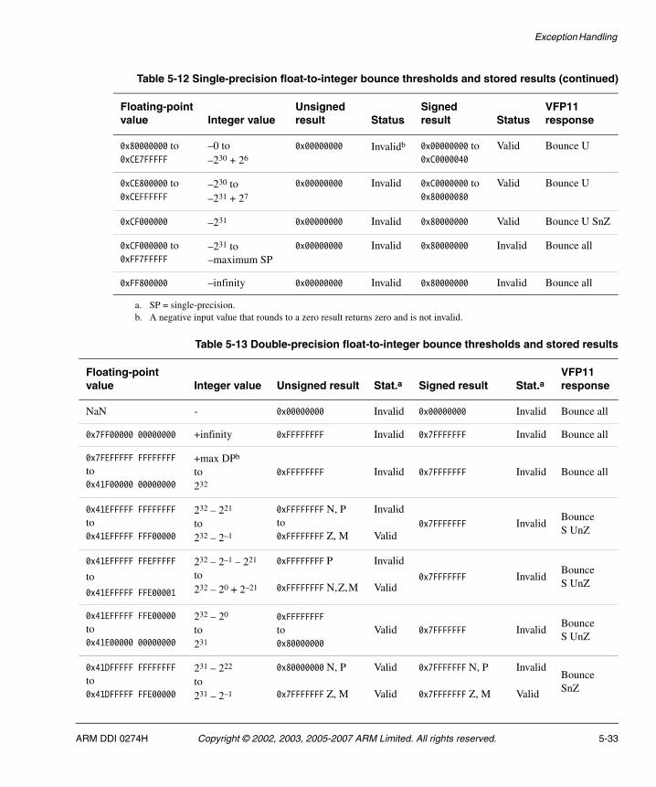
Exception Handling
0x80000000 to 0xCE7FFFFF
–0 to –230 + 26
0x00000000 Invalidb 0x00000000 to 0xC0000040
Valid Bounce U
0xCE800000 to 0xCEFFFFFF
–230 to–231 + 27
0x00000000 Invalid 0xC0000000 to 0x80000080
Valid Bounce U
0xCF000000 –231 0x00000000 Invalid 0x80000000 Valid Bounce U SnZ
0xCF000000 to 0xFF7FFFFF
–231 to –maximum SP
0x00000000 Invalid 0x80000000 Invalid Bounce all
0xFF800000 –infinity 0x00000000 Invalid 0x80000000 Invalid Bounce all
a. SP = single-precision.b. A negative input value that rounds to a zero result returns zero and is not invalid.
Table 5-13 Double-precision float-to-integer bounce thresholds and stored results
Floating-point value Integer value Unsigned result Stat.a Signed result Stat.a
VFP11 response
NaN - 0x00000000 Invalid 0x00000000 Invalid Bounce all
0x7FF00000 00000000 +infinity 0xFFFFFFFF Invalid 0x7FFFFFFF Invalid Bounce all
0x7FEFFFFF FFFFFFFF to 0x41F00000 00000000
+max DPb
to 232
0xFFFFFFFF Invalid 0x7FFFFFFF Invalid Bounce all
0x41EFFFFF FFFFFFFF
to0x41EFFFFF FFF00000
232 – 221
to232 – 2–1
0xFFFFFFFF N, Pto0xFFFFFFFF Z, M
Invalid
Valid0x7FFFFFFF Invalid
Bounce S UnZ
0x41EFFFFF FFEFFFFF
to
0x41EFFFFF FFE00001
232 – 2–1 – 221
to232 – 20 + 2–21
0xFFFFFFFF P
0xFFFFFFFF N,Z,M
Invalid
Valid0x7FFFFFFF Invalid
Bounce S UnZ
0x41EFFFFF FFE00000
to0x41E00000 00000000
232 – 20 to 231
0xFFFFFFFF to 0x80000000
Valid 0x7FFFFFFF InvalidBounce S UnZ
0x41DFFFFF FFFFFFFF
to0x41DFFFFF FFE00000
231 – 222
to231 – 2–1
0x80000000 N, P
0x7FFFFFFF Z, M
Valid
Valid
0x7FFFFFFF N, P
0x7FFFFFFF Z, M
Invalid
Valid
Bounce SnZ
Table 5-12 Single-precision float-to-integer bounce thresholds and stored results (continued)
Floating-point value Integer value
Unsigned result Status
Signed result Status
VFP11 response
ARM DDI 0274H Copyright © 2002, 2003, 2005-2007 ARM Limited. All rights reserved. 5-33

Exception Handling
0x41DFFFFF FFDFFFFF
to0x41DFFFFF FFC00001
231–2–1–2–22
to231–20+2–22
0x80000000 P
0x7FFFFFFF N,Z,M
Valid
Valid
0x7FFFFFFF P
0x7FFFFFFF N,Z,M
Invalid
Valid
Bounce SnZ
0x41DFFFFF FFC00000 to 0x41D00000 00000000
231 – 20 to 230 0x7FFFFFFF to 0x40000000
Valid0x7FFFFFFF to 0x40000000
ValidBounce SnZ
0x41CFFFFF FFFFFFFF
to0x00000000 00000000
230 – 223 to+0
0x40000000 N, P 0x3FFFFFFF Z, M to 0x00000000
ValidValid
0x40000000 N, P0x3FFFFFFF Z, M to 0x00000000
ValidValid
Bounce none
0x80000000 00000000to0xC1CFFFFF FFFFFFFF
–0 to –230+2–23
0x00000000c Invalid0x00000000 to0xC0000001 Z, P0xC0000000 N, M
Valid
ValidBounce U
0xC1D00000 00000000
to0xC1DFFFFF FFFFFFFF
–230 to –231+2–22
0x00000000 Invalid0xC0000000 to0x80000001 Z, P0x80000000 N, M
Valid
ValidBounce U
0xC1E00000 00000000 –231 0x00000000 Invalid 0x80000000 Valid Bounce U SnZ
0xC1E00000 00000001
to0xC1E00000 00100000
–231 – 2–21 to –231 – 2–1
0x00000000 Invalid0x80000000 N, Z, P
0x80000000 M
Valid
Invalid
Bounce U SnZ
0xC1E00000 00100001
to0xC1E00000 001FFFFF
–231–2–1–2–21
to231–20+2–21
0x00000000 Invalid0x80000000 Z, P
0x80000000 N, M
Valid
Invalid
Bounce U SnZ
0xC1E00000 00200000 to 0xFFEFFFFF FFFFFFFF
231 – 20 to –maximum DP
0x00000000 Invalid 0x80000000 Invalid Bounce all
0xFFF00000 00000000 –infinity 0x00000000 Invalid 0x00000000 Invalid Bounce all
a. Status.b. DP = double-precision.c. A negative input value that rounds to a zero result returns zero and is not invalid.
Table 5-13 Double-precision float-to-integer bounce thresholds and stored results (continued)
Floating-point value Integer value Unsigned result Stat.a Signed result Stat.a
VFP11 response
5-34 Copyright © 2002, 2003, 2005-2007 ARM Limited. All rights reserved. ARM DDI 0274H

Glossary
This glossary defines some of the terms used in this manual.
Arithmetic instruction
Any VFPv2 Coprocessor Data Processing (CDP) instruction except FCPY, FABS, and FNEG.
See also CDP instruction.
Bounce The VFP11 coprocessor bounces an instruction when it fails to signal the acceptance of a valid VFP instruction to the ARM11 processor. This action initiates Undefined Instruction processing by the ARM11 processor. The VFP support code is called to complete the instruction that was found to be exceptional or unsupported by the VFP11 coprocessor.
See also Trigger instruction, Potentially exceptional instruction, and Exceptional state.
CDP instruction Coprocessor data processing instruction. For the VFP11 coprocessor, CDP instructions are arithmetic instructions and FCPY, FABS, and FNEG.
See also Arithmetic instruction.
Default NaN mode A mode in which all operations that result in a NaN return the default NaN, regardless of the cause of the NaN result. This mode is compliant with the IEEE 754 standard but implies that all information contained in any input NaNs to an operation is lost.
Denormalized value See Subnormal value.
ARM DDI 0274H Copyright © 2002, 2003, 2005-2007 ARM Limited. All rights reserved. Glossary-1

Glossary
Disabled exception An exception is disabled when its exception enable bit in the FPCSR is not set. For these exceptions, the IEEE 754 standard defines the result to be returned. An operation that generates an exception condition can bounce to the support code to produce the result defined by the IEEE 754 standard. The exception is not reported to the user trap handler.
Enabled exception An exception is enabled when its exception enable bit in the FPCSR is set. When an enabled exception occurs, a trap to the user handler is taken. An operation that generates an exception condition might bounce to the support code to produce the result defined by the IEEE 754 standard. The exception is then reported to the user trap handler.
Exceptional state When a potentially exceptional instruction is issued, the VFP11 coprocessor sets the EX bit, FPEXC[31], and loads a copy of the potentially exceptional instruction in the FPINST register. If the instruction is a short vector operation, the register fields in FPINST are altered to point to the potentially exceptional iteration. When in the exceptional state, the issue of a trigger instruction to the VFP11 coprocessor causes a bounce.
See also Bounce, potentially exceptional instruction, and trigger instruction.
Exponent The component of a floating-point number that normally signifies the integer power to which two is raised in determining the value of the represented number.
Fd The destination register and the accumulate value in triadic operations. Sd for single-precision operations and Dd for double-precision.
Flush-to-zero mode In this mode, the VFP11 coprocessor treats the following values as positive zeros:
• arithmetic operation inputs that are in the subnormal range for the input precision
• arithmetic operation results, other than computed zero results, that are in the subnormal range for the input precision before rounding.
The VFP11 coprocessor does not interpret these values as subnormal values or convert them to subnormal values.
The subnormal range for the input precision is –2Emin < x < 0 or 0< x < 2Emin.
Fm The second source operand in dyadic or triadic operations. Sm for single-precision operations and Dm for double-precision
Fn The first source operand in dyadic or triadic operations. Sn for single-precision operations and Dn for double-precision.
Fraction The floating-point field that lies to the right of the implied binary point.
Glossary-2 Copyright © 2002, 2003, 2005-2007 ARM Limited. All rights reserved. ARM DDI 0274H

Glossary
IEEE 754 standard IEEE Standard for Binary Floating-Point Arithmetic, ANSI/IEEE Std 754-1985. The standard that defines data types, correct operation, exception types and handling, and error bounds for floating-point systems. Most processors are built in compliance with the standard in either hardware or a combination of hardware and software.
Illegal instruction An instruction that is architecturally Undefined.
Infinity In the IEEE 754 standard format to represent infinity, the exponent is the maximum for the precision and the fraction is all zeros.
Input exception A VFP exception condition in which one or more of the operands for a given operation are not supported by the hardware. The operation bounces to support code for processing.
Intermediate result An internal format used to store the result of a calculation before rounding. This format can have a larger exponent field and fraction field than the destination format.
MCR/MCRR A class of data transfer instructions that transfer 32-bit or 64-bit quantities from ARM registers to VFP11 registers.
MRC/MRRC A class of data transfer instructions that transfer 32-bit or 64-bit quantities from VFP11 registers to ARM registers.
NaN Not a number. A symbolic entity encoded in a floating-point format that has the maximum exponent field and a nonzero fraction. An SNaN causes an invalid operand exception if used as an operand and a most significant fraction bit of zero. A QNaN propagates through almost every arithmetic operation without signaling exceptions and has a most significant fraction bit of one.
Potentially exceptional instruction
An instruction that is determined, based on the exponents of the operands and the sign bits, to have the potential to produce an overflow, underflow, or invalid condition. After this determination is made, the instruction that has the potential to cause an exception causes the VFP11 coprocessor to enter the exceptional state and bounce the next trigger instruction issued.
See also Bounce, Trigger instruction, and Exceptional state.
Register banks Four banks of registers for both scalar and short vector floating-point operations. In single-precision operations, each bank contains eight single-precision registers. In double-precision operations, each bank contains four double-precision registers.
Reserved A field in a control register or instruction format is reserved if the field is to be defined by the implementation, or produces Unpredictable results if the contents of the field are not zero. These fields are reserved for use in future extensions of the architecture or are implementation-specific. All reserved bits not used by the implementation must be written as 0 and read as 0.
ARM DDI 0274H Copyright © 2002, 2003, 2005-2007 ARM Limited. All rights reserved. Glossary-3

Glossary
Rounding mode The IEEE 754 standard requires all calculations to be performed as if to an infinite precision. For example, a multiply of two single-precision values must accurately calculate the significand to twice the number of bits of the significand. To represent this value in the destination precision, rounding of the significand is often required. The IEEE 754 standard specifies four rounding modes:
• In round-to-nearest mode, the result is rounded at the halfway point, with the tie case rounding up if it would clear the least significant bit of the significand, making it even.
• Round-towards-zero mode chops any bits to the right of the significand, always rounding down, and is used by the C, C++, and Java languages in integer conversions.
• Round-towards-plus-infinity mode and round-towards-minus-infinity mode are used in interval arithmetic.
RunFast mode In RunFast mode, hardware handles exceptional conditions and special operands. RunFast mode is enabled by enabling default NaN and flush-to-zero modes and disabling all exceptions. In RunFast mode, the VFP11 coprocessor does not bounce to the support code for any legal operation or any operand, but supplies a result to the destination. For all inexact and overflow results and all invalid operations that result from operations not involving NaNs, the result is as specified by the IEEE 754 standard. For operations involving NaNs, the result is the default NaN.
Scalar operation A VFP coprocessor operation involving a single source register and a single destination register.
See also Vector operation.
Short vector operation
A VFP coprocessor operation involving more than one destination register and perhaps more than one source register in the generation of the result for each destination.
Significand The component of a binary floating-point number that consists of an explicit or implicit leading bit to the left of the implied binary point and a fraction field to the right.
Stride The stride field, FPSCR[21:20], specifies the increment applied to register addresses in short vector operations. A stride of 00, specifying an increment of +1, causes a short vector operation to increment each vector register by +1 for each iteration, while a stride of 11 specifies an increment of +2.
Subnormal value A value in the range (–2Emin < x < 2Emin), except for ±0. In the IEEE 754 standard format for single-precision and double-precision operands, a subnormal value has a zero exponent and a nonzero fraction field. The IEEE 754 standard requires that the generation and manipulation of subnormal operands be performed with the same precision as normal operands.
Glossary-4 Copyright © 2002, 2003, 2005-2007 ARM Limited. All rights reserved. ARM DDI 0274H

Glossary
Support code Software that must be used to complement the hardware to provide compatibility with the IEEE 754 standard. The support code has a library of routines that performs supported functions, such as divide with unsupported inputs or inputs that might generate an exception as well as operations beyond the scope of the hardware. The support code has a set of exception handlers to process exceptional conditions in compliance with the IEEE 754 standard.
Tiny A nonzero result or value that is between the positive and negative minimum normal values for the destination precision.
Trap A exceptional condition that has the respective exception enable bit set in the FPSCR register. The user trap handler is executed.
Trigger instruction The VFP coprocessor instruction that causes a bounce at the time it is issued. A potentially exceptional instruction causes the VFP11 coprocessor to enter the exceptional state. A subsequent instruction, unless it is an FMXR or FMRX instruction accessing the FPEXC, FPINST, or FPSID register, causes a bounce, beginning exception processing. The trigger instruction is not necessarily exceptional, and no processing of it is performed. It is retried at the return from exception processing of the potentially exceptional instruction.
See also Bounce, Potentially exceptional instruction, and Exceptional state.
UND See Undefined.
Undefined (UND) Indicates an instruction that generates an Undefined instruction trap. See the ARM Architecture Reference Manual for more information on ARM exceptions.
UNP See Unpredictable.
Unpredictable (UNP)For reads, the data returned when reading from this location is unpredictable. It can have any value. For writes, writing to this location causes unpredictable behavior, or an unpredictable change in device configuration. Unpredictable instructions must not halt or hang the processor, or any part of the system
Unsupported values Specific data values that are not processed by the VFP coprocessor hardware but bounced to the support code for completion. These data can include infinities, NaNs, subnormal values, and zeros. An implementation is free to select which of these values is supported in hardware fully or partially, or requires assistance from support code to complete the operation. Any exception resulting from processing unsupported data is trapped to user code if the corresponding exception enable bit for the exception is set.
Vector operation A VFP coprocessor operation involving more than one destination register, perhaps involving different source registers in the generation of the result for each destination.
See also Scalar operation.
ARM DDI 0274H Copyright © 2002, 2003, 2005-2007 ARM Limited. All rights reserved. Glossary-5

Glossary
Glossary-6 Copyright © 2002, 2003, 2005-2007 ARM Limited. All rights reserved. ARM DDI 0274H