Embed Size (px)
Citation preview

VARIATION AND POWER ISSUES IN VLSI CLOCK NETWORKS
A Dissertation
by
GANESH VENKATARAMAN
Submitted to the Office of Graduate Studies ofTexas A&M University
in partial fulfillment of the requirements for the degree of
DOCTOR OF PHILOSOPHY
May 2007
Major Subject: Computer Engineering
VARIATION AND POWER ISSUES IN VLSI CLOCK NETWORKS
A Dissertation
by
GANESH VENKATARAMAN
Submitted to the Office of Graduate Studies ofTexas A&M University
in partial fulfillment of the requirements for the degree of
DOCTOR OF PHILOSOPHY
Approved by:
Chair of Committee, Jiang HuCommittee Members, Sunil Khatri
Vivek SarinWeiping Shi
Head of Department, Costas N. Georghiades
May 2007
Major Subject: Computer Engineering

iii
ABSTRACT
Variation and Power Issues in VLSI Clock Networks. (May 2007)
Ganesh Venkataraman, B. E. (Hons), Birla Institute of Technology and Science;
M. Sc. (Hons), Birla Institute of Technology and Science;
M. S., University of Iowa
Chair of Advisory Committee: Dr. Jiang Hu
Clock Distribution Network (CDN) is an important component of any syn-
chronous logic circuit. The function of CDN is to deliver the clock signal to the clock
sinks. Clock skew is defined as the difference in the arrival time of the clock signal at
the clock sinks. Higher uncertainty in skew (due to PVT variations) degrades circuit
performance by decreasing the maximum possible delay between any two sequential
elements. Aggressive frequency scaling has also led to high power consumption espe-
cially in CDN. This dissertation addresses variation and power issues in the design of
current and potential future CDN. The research detailed in this work presents algo-
rithmic techniques for the following problems: (1) Variation tolerance in useful skew
design, (2) Link insertion for buffered clock nets, (3) Methodology and algorithms for
rotary clocking and (4) Clock mesh optimization for skew-power trade off.
For clock trees this dissertation presents techniques to integrate the different
aspects of clock tree synthesis (skew scheduling, abstract topology and layout embed-
ding) into one framework - tolerance to variations. This research addresses the issues
involved in inserting cross-links in a buffered clock tree and proposes design criteria
to avoid the risk of short-circuit current. Rotary clocking is a promising new clocking
scheme that consists of unterminated rings formed by differential transmission lines.
Rotary clocking achieves reduction in power dissipation clock skew. This dissertation
addresses the issues in adopting current CAD methodology to rotary clocks. Alter-

iv
native methodology and corresponding algorithmic techniques are detailed. Clock
mesh is a popular form of CDN used in high performance systems. The problem
of simultaneous sizing and placement of mesh buffers in a clock mesh is addressed.
The algorithms presented remove the edges from the clock mesh to trade off skew
tolerance for low power.
For clock trees as well as link insertion, our experiments indicate significant re-
duction in clock skew due to variations. For clock mesh, experimental results indicate
18.5% reduction in power with 1.3% delay penalty on a average. In summary, this dis-
sertation details methodologies/algorithms that address two critical issues - variation
and power dissipation in current and potential future CDN.

v
To my grandparents, parents and in special memory of my grandmom

vi
ACKNOWLEDGMENTS
I must thank Dr. Jiang Hu for his guidance and support. He introduced me to
Physical Design and served as a constant source of encouragement throughout my
stay at Texas A&M.
I would like to thank the Semiconductor Research Corporation (SRC) for sup-
porting my research. Many thanks to the Office of Graduate Studies at Texas A&M
for granting the Graduate Merit Fellowship.
I have been fortunate enough to work with and learn from different professors
and students throughout my doctoral studies. I would like to thank Dr. Sunil Khatri
and Nikhil Jayakumar for helping me out with the link insertion work as well as some
insightful discussions. I enjoyed working with Dr. Peng Li on developing driver models
for fast simulation of clock mesh. Dr. Li’s course introduced me to the exciting area of
circuit simulation. I would like to thank Dr. Weiping Shi for teaching some very fine
algorithmic concepts in VLSI CAD and for serving on my dissertation committee.
I would like to thank Dr. Vivek Sarin for serving on my dissertation committee.
The basic idea for clock mesh optimization was inspired from a lecture by Dr. Alex
Sprintson. I would like to thank Dr. Sprintson for all the discussions. I am thankful to
all my teachers - right from kindergarden for passing on their knowledge and wisdom.
I am deeply indebted to my uncle Dr. S. V. Ramakrishnan and aunt Mrs. Sita
Ramakrishnan for their love and support. I would like to thank my grandparents for
their incredible love. I would like to thank my parents, my brother and his wife for
just about everything.

vii
TABLE OF CONTENTS
CHAPTER Page
I INTRODUCTION . . . . . . . . . . . . . . . . . . . . . . . . . . 1
A. Background and Motivation . . . . . . . . . . . . . . . . . 1
1. Impact of PVT Variations on Clock Skew . . . . . . . 3
2. Power Dissipation in CDN . . . . . . . . . . . . . . . 3
B. Contributions . . . . . . . . . . . . . . . . . . . . . . . . . 4
1. Variation Tolerance in Useful Skew Design . . . . . . . 4
2. Link Insertion for Buffered Clock Nets . . . . . . . . . 5
3. Methodology and Algorithms for Rotary Clocking . . 6
4. Combinatorial Algorithms for Fast Clock Mesh Op-
timization . . . . . . . . . . . . . . . . . . . . . . . . . 8
C. Organization . . . . . . . . . . . . . . . . . . . . . . . . . . 9
II VARIATION TOLERANCE IN USEFUL SKEW DESIGN . . . 10
A. Preliminaries . . . . . . . . . . . . . . . . . . . . . . . . . 10
B. Previous Work . . . . . . . . . . . . . . . . . . . . . . . . . 11
C. Problem Statement . . . . . . . . . . . . . . . . . . . . . . 15
D. Algorithm . . . . . . . . . . . . . . . . . . . . . . . . . . . 15
1. Algorithm Overview . . . . . . . . . . . . . . . . . . . 15
2. Process Variation Aware Skew Scheduling . . . . . . . 17
3. Process Variation Aware Layout Embedding . . . . . . 18
4. Alternative Layout Embedding . . . . . . . . . . . . . 23
5. Abstract Tree Generation . . . . . . . . . . . . . . . . 24
6. Algorithm Complexity . . . . . . . . . . . . . . . . . . 24
E. Experimental Results . . . . . . . . . . . . . . . . . . . . . 25
III LINK INSERTION IN BUFFERED CLOCK NETS . . . . . . . 30
A. Preliminaries . . . . . . . . . . . . . . . . . . . . . . . . . 30
B. Previous Work . . . . . . . . . . . . . . . . . . . . . . . . . 31
C. Problem Statement . . . . . . . . . . . . . . . . . . . . . . 33
D. Multi-driver Nets . . . . . . . . . . . . . . . . . . . . . . . 33
1. Short Circuit Avoidance . . . . . . . . . . . . . . . . . 34
2. Multi-driver Delay Analysis . . . . . . . . . . . . . . . 35
E. Localized Skew Tuning . . . . . . . . . . . . . . . . . . . . 36

viii
CHAPTER Page
F. Link Based Buffered Clock Network Construction . . . . . 38
1. Buffered Clock Tree Construction . . . . . . . . . . . 38
2. Impact of Tunable Buffers and Delay Balancing . . . . 40
3. Link Insertion . . . . . . . . . . . . . . . . . . . . . . 43
G. Experiment . . . . . . . . . . . . . . . . . . . . . . . . . . 46
1. Experiment Setup . . . . . . . . . . . . . . . . . . . . 46
2. Experiment Design . . . . . . . . . . . . . . . . . . . . 47
3. Experimental Results . . . . . . . . . . . . . . . . . . 48
IV METHODOLOGY AND ALGORITHMS FOR ROTARY CLOCK-
ING . . . . . . . . . . . . . . . . . . . . . . . . . . . . . . . . . 55
A. Previous Work . . . . . . . . . . . . . . . . . . . . . . . . . 55
B. Rotary Traveling Wave Clock and Traditional Design Flow 57
C. Relaxation via Flexible Tapping . . . . . . . . . . . . . . . 60
D. Proposed Methodology . . . . . . . . . . . . . . . . . . . . 63
E. Flip-flop Assignment to Minimize Tapping Cost . . . . . . 65
F. Flip-flop Assignment to Minimize Load Capacitance . . . . 66
1. Solution by LP-relaxation . . . . . . . . . . . . . . . . 67
G. Skew Optimization . . . . . . . . . . . . . . . . . . . . . . 70
H. Experimental Results . . . . . . . . . . . . . . . . . . . . . 73
V COMBINATORIAL ALGORITHMS FOR FAST CLOCK MESH
OPTIMIZATION . . . . . . . . . . . . . . . . . . . . . . . . . . 82
A. Preliminaries . . . . . . . . . . . . . . . . . . . . . . . . . 82
B. Previous Work . . . . . . . . . . . . . . . . . . . . . . . . . 83
C. Problem Statement . . . . . . . . . . . . . . . . . . . . . . 86
D. Simultaneous Mesh Buffer Placement and Sizing via Set Cover 87
1. Algorithm Description . . . . . . . . . . . . . . . . . . 87
2. Complexity Analysis and Near-Continuous Sizing . . . 91
E. Mesh Reduction and Post-Processing . . . . . . . . . . . . 93
1. Mesh Reduction . . . . . . . . . . . . . . . . . . . . . 93
2. Post-Processing for Mesh Reduction . . . . . . . . . . 96
F. Experimental Results . . . . . . . . . . . . . . . . . . . . . 99
1. Experiment Set up . . . . . . . . . . . . . . . . . . . . 99
2. Experiment Design . . . . . . . . . . . . . . . . . . . . 100
3. Results . . . . . . . . . . . . . . . . . . . . . . . . . . 101

ix
CHAPTER Page
VI CONCLUSIONS . . . . . . . . . . . . . . . . . . . . . . . . . . . 112
REFERENCES . . . . . . . . . . . . . . . . . . . . . . . . . . . . . . . . . . . 115
VITA . . . . . . . . . . . . . . . . . . . . . . . . . . . . . . . . . . . . . . . . 123
x
LIST OF TABLES
TABLE Page
I Results for the base case. . . . . . . . . . . . . . . . . . . . . . . . . 26
II Single pair and multiple pair embedding schemes - when abstract
topology is distance based. . . . . . . . . . . . . . . . . . . . . . . . . 28
III Single pair and multiple pair embedding schemes - when abstract
topology is embedding aware. . . . . . . . . . . . . . . . . . . . . . . 29
IV Comparison between snaking and delay balancing. . . . . . . . . . . 43
V Results for clock trees without delay balancing, without tuning. . . . 50
VI Comparison between (delay balancing, no tuning) vs (no delay
balancing, no tuning). . . . . . . . . . . . . . . . . . . . . . . . . . . 51
VII Comparison between (delay balancing, WITH tuning) vs (delay
balancing WITHOUT tuning). . . . . . . . . . . . . . . . . . . . . . 52
VIII Variation results for clock trees with delay balancing and tuning. . . 53
IX Variation/resource comparison between links and clock trees. . . . . 53
X Variation/resource comparison between mesh and clock trees. . . . . 54
XI Integrality gap of greedy rounding and ILP-solver. . . . . . . . . . . 70
XII Testcases. PL is the average source-sink path length in conven-
tional clock trees [17, 20]. . . . . . . . . . . . . . . . . . . . . . . . . 74
XIII Experimental results for the base case, wirelength in µm, power in mW . 77
XIV Experimental results for network flow based optimization, wire-
length in µm. . . . . . . . . . . . . . . . . . . . . . . . . . . . . . . . 78
XV Comparison of network flow and ILP formulations, cap in pF . . . . . 79
xi
TABLE Page
XVI Power dissipation results (mW ) for network flow and ILP formulations. 80
XVII Wirelength capacitance product comparison. . . . . . . . . . . . . . . 81
XVIII Benchmark characteristics. . . . . . . . . . . . . . . . . . . . . . . . . 99
XIX Results for the buffer placement/sizing algorithm. . . . . . . . . . . . 103
XX Results for uniform sizing - smallest size. . . . . . . . . . . . . . . . . 104
XXI Results for uniform sizing - medium buffer size. . . . . . . . . . . . . 105
XXII Results for uniform sizing - largest buffer size. . . . . . . . . . . . . . 106
XXIII Results for mesh reduction. . . . . . . . . . . . . . . . . . . . . . . . 110
XXIV Reduction in buffer area and power after post-processing. . . . . . . . 111

xii
LIST OF FIGURES
FIGURE Page
1 Overview of the contributions. . . . . . . . . . . . . . . . . . . . . . . 5
2 Merging and embedding of subtrees. . . . . . . . . . . . . . . . . . . 13
3 Scheduling and routing algorithm. . . . . . . . . . . . . . . . . . . . 16
4 Plot of Sij with two pairs. . . . . . . . . . . . . . . . . . . . . . . . . 23
5 If there is significant difference ∆ between signal arrival time to
the two drivers, there is risk of short circuit indicated by the
dashed line. . . . . . . . . . . . . . . . . . . . . . . . . . . . . . . . . 34
6 The dual driver net in (a) can be converted to the single driver
net in (b) when signal departure time t1 at node 1 is no less than
the signal departure time t2 at node 2. . . . . . . . . . . . . . . . . . 36
7 Tuning the location of merging node m3 in a buffered clock tree
falls into a cyclic dependency. . . . . . . . . . . . . . . . . . . . . . . 37
8 Tunable clock buffer. . . . . . . . . . . . . . . . . . . . . . . . . . . . 38
9 Link insertion in buffered clock tree. Dashed lines indicate links. . . . 39
10 Merging subtrees for zero skew tree. . . . . . . . . . . . . . . . . . . 40
11 Algorithm of selecting node pairs between two subtrees. . . . . . . . 44
12 (a) A rotary clock ring. The numbers indicate relative clock signal
phase. (b) An array of 13 rotary clock rings. The small triangles
points to the equal-phase points for the 13 rings. . . . . . . . . . . . 55
13 The tapping point p for a flip-flop can be found by solving the
delay satisfying clock signal delay target. . . . . . . . . . . . . . . . . 60
14 Proposed methodology flow. . . . . . . . . . . . . . . . . . . . . . . . 63

xiii
FIGURE Page
15 Min-cost network flow model for flip-flop assignment. Each arc is
associated with cost/capacity. . . . . . . . . . . . . . . . . . . . . . . 65
16 Greedy rounding algorithm. . . . . . . . . . . . . . . . . . . . . . . . 70
17 Mesh driven by a top level tree. . . . . . . . . . . . . . . . . . . . . . 83
18 Overall flow for mesh buffer sizing and reduction. . . . . . . . . . . . 88
19 Example of covering region. . . . . . . . . . . . . . . . . . . . . . . . 90
20 Greedy set cover for mesh buffer placement/sizing. . . . . . . . . . . 92
21 CPU time vs # buffer types for s35932. . . . . . . . . . . . . . . . . 93
22 Simple example for mesh reduction. . . . . . . . . . . . . . . . . . . . 95
23 Greedy mesh reduction. . . . . . . . . . . . . . . . . . . . . . . . . . 97
24 Post processing after mesh reduction. . . . . . . . . . . . . . . . . . . 98
25 Worst case output waveform with small buffer size. . . . . . . . . . . 108
26 Worst case output waveform with medium buffer size. . . . . . . . . 109
27 Worst case output waveform with large buffer size. . . . . . . . . . . 109
28 Worst case output waveform with sizing algorithm. . . . . . . . . . . 109
29 Power vs. skewmax trade off for s9234 . . . . . . . . . . . . . . . . . 111

1
CHAPTER I
INTRODUCTION
A. Background and Motivation
Millions of transistors running in tandem have had a significant impact on our day-
to-day life. Very Large Scale Integration (VLSI) is the process of creating Integrated
Circuits (IC) by combining thousands of transistors on a single chip. The design, im-
plementation, manufacturing and testing of VLSI circuits are done using automated
computational techniques along with manual intervention as and when deemed nec-
essary. The area of study devoted to developing algorithmic techniques and method-
ologies towards automating electronic design is commonly referred to as Electronic
Design Automation (EDA).
For nearly three decades, the trend in the growth of IC design was dictated by
an empirical observation also known as the Moore’s Law. Moore’s Law states that
the number of transistors in a chip doubles every 18 months implying an exponential
growth in transistor count. The operating frequency has so far been following the
same trend. A key enabler of this rapid frequency scaling is constant reduction in
minimum channel length of the CMOS transistor with every process generation. With
every process generation also comes a new set of challenges for EDA. The function
of EDA research is not just to solve the current problems but also identify the issues
that may arise with future technologies. VLSI design involves multiple objectives
like timing, power dissipation, area, manufacturing yield, testability etc. Very often
these objectives might conflict with each other. A common example with conflicting
objectives is power dissipation and circuit delay. Higher gate sizes could reduce circuit
The journal model is IEEE Transactions on Automatic Control.

2
delay at the expense of higher power. EDA tools should also have the capability to
trade off one objective for another and should allow the designer the flexibility to
choose the desired trade off point.
Clock Distribution Network (CDN) is an integral part of any synchronous logic
circuit. The function of CDN is to deliver the clock signal to the sequential elements.
These elements are also referred to in literature as clock registers, flip-flops or clock
sinks - all referring to the final destination of the clock signal. Clock skew between
two clock sinks is defined as the difference between the arrival time of the clock signal
at corresponding two clock sinks. Let ti denote the arrival time of the clock signal at
sink i. In order to avoid a logic failure the skew between a register pair (i, j) should
be within the followings limits [1]:
thold −Dijmin ≤ ti − tj ≤ Tclock − tsetup −Dij
max (1.1)
In the above equation, Tclock, thold and tsetup denote the clock period, hold time and set
up time respectively. Dijmax (Dij
min) denotes the maximum (minimum) combinational
delay between i and j. Based on the assignment of arrival times, there are two types of
CDN design: (1) Useful skew (also referred to as intentional skew) design, where clock
skew is exploited to optimize design objectives such as wire length, clock frequency,
tolerance of variations etc. (2) Zero Skew design, there CDN is constructed such
that the arrival time of the clock signal at all the clock sinks is the same. For zero
skew design, it is evident from Equation (1.1) that higher skew reduces the maximum
delay possible between two sequential elements (implies a reduction in maximum
circuit delay).

3
1. Impact of PVT Variations on Clock Skew
Process, voltage and temperature (often referred to as PVT) variations are becoming
prominent factors that affect the design parameters of modern VLSI chips. Clock
skew is a design parameter that is highly sensitive to PVT variations. On analyzing
the impact of variations on the clock skew of a gigahertz microprocessor, it was
observed that interconnect variations alone can cause up to 25% variation in clock
skew [2]. Apart from interconnect, variation in clock skew can also occur from the
following factors (1) power supply (2) clock buffer channel length and (3) sink load
capacitance. Clock buffers are required to meet the constraints on signal slew and
delay. The percentage of clock sinks in the total cell count keeps increasing with the
successive process technologies. It has been projected that this number could rise to
as much as 18.55% in future technologies [3]. Higher number of clock sinks implies
that we would need larger number of clock buffers to drive the clock net. This will
mean larger variations in clock skew. Further, a 10% drop in power grid voltage (IR-
drop) could cause 5-10% change in clock timing [4]. Further, the impact of IR-drop
gets worst as voltage is scaled down. In summary, clock skew is susceptible to PVT
variations and the effect is getting worst with technology scaling.
2. Power Dissipation in CDN
In CMOS, dynamic power is dissipated when the output switches value. The dynamic
power dissipation is given by:
Pdynamic =1
2SfV
2ddfclkCload (1.2)
In the above equation Vdd denotes the supply voltage, fclk the clock frequency, Cload
the load capacitance and Sf the switching activity. For signal nets, Sf is usually

4
between 0.10 and 0.20 [5]. The clock net switches every cycle. Hence, the switching
activity equals 1 and this accounts for high power dissipation in the clock net. In high
performance systems, the clock net could account for as much as 40% of the total
power dissipation [6]. With the percentage of clock sinks increasing with every process
generation [3], this figure could get higher. While power dissipation is of paramount
importance in portable electronic devices, it has now become a significantly important
design objective in high performance systems as well. Examples of such high perfor-
mance systems include laptop computers (low power implies longer battery life) and
server farms (commonly used in Internet search engines). In summary, the impor-
tance of power dissipation in VLSI design is becoming increasingly important. Since
the clock net consumes a major portion of the total power dissipation, it is imperative
to address this issue in EDA research.
B. Contributions
This dissertation deals with two keys in the design of modern CDN - variation and
power dissipation. Figure (1) gives the overview of our contributions classified on
the basis of different types of clock distributions. Our main contributions include (1)
Variation tolerance in useful skew design (2) Link insertion for buffered clock nets,
(3) Methodology and algorithms for rotary clocking and (4) Clock mesh optimization
for skew-power trade off.
1. Variation Tolerance in Useful Skew Design
Useful skew design consists of manipulating the clock skew in order to achieve the
design objectives [7], such as high frequency and variation tolerance. We integrate all
the above three steps namely - clock skew scheduling, abstract topology construction

5
Tree: Rotary Clocking:
Clock Distribution Network
Placement and schedulingmethodology
Combinatorial algorithms forBuffered NetworksExtend Link Insertion forNon Tree:
fast clock mesh optimization
useful skew designVariation tolerance in
Fig. 1. Overview of the contributions.
and layout embedding in to one framework. The objective of the work is to minimize
the maximum skew due to variations. In skew scheduling, an estimation of variations
based on clock sink locations is employed to guide skew safety margin towards sink
pairs which are more vulnerable to variations. Abstract topology is generated based
on the estimated delay targets. In clock routing, an embedding technique is developed
to minimize the maximum skew violation among all sink pairs optimally.
2. Link Insertion for Buffered Clock Nets
Link insertion refers to the process of adding cross-links to a clock tree thereby con-
verting it into a non-tree. The primary purpose of link insertion is to improve the
tolerance of the tree towards variations in clock skew. Link insertion has been shown
to provide an effective trade off between skew reduction and increase in wire length.
Previous works on link insertion focused on unbuffered clock networks [8, 9]. In re-
ality, buffers are required to meet constraints on signal slew and delay. The main
contributions of the work include:
• Link insertion in a buffered network may result in multiple drivers for a subnet.

6
A design criterion for avoiding short circuit risk in a multi-driver net is proposed.
• Skew tuning is used to synthesize a clock tree with low nominal skew under a
higher order delay model. The effect of link insertion depends on a well-designed
buffered clock tree. The proposed technique can decrease nominal clock skew
considerably and therefore enhances the effectiveness of link insertion.
• A complete methodology of link based buffered clock network under accurate
gate and wire delay models is proposed. This methodology utilizes the buffered
clock tree construction techniques which are friendly to link insertion.
• The proposed method is validated with HSPICE based Monte Carlo simulations
considering spatially correlated power supply variations, buffer and wire process
variations.
3. Methodology and Algorithms for Rotary Clocking
In order to solve the power and the variation problem more effectively, several novel
clocking technologies have been developed. Among them, rotary traveling wave clock
is a promising approach [10]. The basic component of a rotary clock is a pair of
cross-connected differential transmission line circles, namely a rotary clock ring. A
clock signal propagates along the ring without termination so that the energy can be
recirculated and the charging/discharging power dissipation is greatly reduced.
There is one technical hurdle that prevents wide applications of the rotary clock:
the clock signal has different phases at different locations on the rotary clock ring.
If zero skew design is insisted, the usage of rotary clocks would be very restrictive.
Hence, non-zero intentional skew design is a better approach to fully utilize the ro-
tary clock. Unlike the intentional skew design in the conventional clocking technology
where no restrictions are imposed on the flip-flop locations, the skew at each flip-flop

7
has to be matched with a specific location at the rotary clock ring. This requirement
forms a difficult chicken-and-egg problem: the flip-flop placement depends on skew
optimization while it is well known that skew optimization depends on flip-flop lo-
cations. This is quite different from traditional intentional skew designs where the
placement does not depend on skew optimization.
We make the following contributions:
• A relaxation technique based on flexible tapping is suggested to break the loop
in the chicken-and-egg problem.
• An integrated placement and skew optimization methodology is proposed to
facilitate the application of rotary clocking. This methodology has the advan-
tage that traditional placement methods can be employed directly without any
change.
• A min-cost network flow algorithm is found to assign flip-flops to the rotary clock
rings so that the movement of flip-flops has the least disturbance to traditional
placement.
• A pseudo net technique is introduced to guide flip-flops toward their preferred
locations without intrusive disturbance to traditional placement.
• A cost driven skew optimization formulation is developed to reduce the connec-
tion cost between flip-flops and their corresponding rotary clock rings.
Our techniques can be easily augmented with existing CAD tools/flow thereby making
rotary clocks usable for practical designs.

8
4. Combinatorial Algorithms for Fast Clock Mesh Optimization
Clock mesh is a popular form of CDN used in high performance systems [11, 12, 13].
Mesh has a high tolerance to variations. The tolerance comes from the redundancy
created by the multiple paths between the clock source and the sinks. However, such
a high tolerance comes at an expense of increased resource consumption - namely
high wire length and power dissipation. Mesh is usually driven by a top-level tree
with buffers at the leaves of the this tree - henceforth referred to as mesh buffers.
Previous works on clock mesh do not address the issue of where to place the mesh
buffers in the clock mesh. It is also not clear if there is a scope to use buffers of
different size. We address the issue of mesh buffer sizing as well as their placement
in the mesh. We then remove the edges in the mesh to trade off the skew tolerance
for lower power dissipation. Our contributions include:
• We propose a set-cover based algorithm for finding the mesh buffer locations
and their sizes. Our algorithm works fast on a discrete library of buffer sizes.
We show that such a buffer placement and sizing yields better results compared
to uniform sizing.
• We formulate the mesh reduction problem by using survivable network theory.
We present heuristics for solving the formulation efficiently.
• Our techniques allow the designer to trade off between skew and power dissipa-
tion. In fact, the formulation presented is flexible enough to allow a high range
of trade off (that is either a high skew- low power design or a low skew - high
power design or anywhere in between).
• Our algorithms run very fast. It can process test cases with over a thousand
sinks within a few seconds. Such a high speed helps the designer to run the same

9
algorithm several times with different parameter values that produce different
solutions in the power delay curve.
C. Organization
The remainder of this dissertation is organized as follows. Chapter II deals with
variation tolerance in useful skew design. We detail some of the problems encountered
while inserting links in buffered clock nets in Chapter III. We then proceed to describe
our procedure for clock tree generation as well as link insertion. Chapter IV details
the issues involved in adopting the current CAD methodologies for rotary clocking.
We then propose our flow and corresponding algorithms. Chapter V details our
work on clock mesh optimization. We present fast algorithms for simultaneous mesh
buffer placement and sizing. This chapter also presents mesh reduction techniques.
Chapter VI details our conclusions.

10
CHAPTER II
VARIATION TOLERANCE IN USEFUL SKEW DESIGN
This chapter details our techniques that improve variation tolerance in useful skew
design. The objective of the work is to minimize the maximum deviation of clock
skew from the allowed limits.
A. Preliminaries
The following notations/conventions will be followed in this chapter:
• Clock sinks, registers and flip-flops refer to sequential elements unless otherwise
specified.
• Two clock sinks are said to be sequentially adjacent if they have only com-
binational logic between them.
• S = s1, s2, ...sn denotes the set of clock sinks.
• Ci denotes the sink load capacitance.
• For each sink i, ti denotes the signal arrival time.
• Tclock, thold and tsetup denote the clock period, hold time and set up time respec-
tively.
• Dijmax (Dij
min) denotes the maximum (minimum) combinational delay between
sinks i and j.
• In order to avoid a logic failure the skew between a register pair (i, j) should be
within the followings limits [1]:
thold −Dijmin ≤ ti − tj ≤ Tclock − tsetup −Dij
max (2.1)

11
• tl(i, j) = thold−Dmin and tu(i, j) = T − tsetup−Dmax form the lower and upper
skew permissible range respectively.
• w denotes the wire width.
• The capacitance of an interconnect of length l is given by c·l ·w, where c denotes
the capacitance per unit area.
• The resistance of an interconnect of length l is given by r · lw
where r denotes
the sheet resistance.
• We assume the wire width and sink load variations follow normal distributions
and the variation is approximately bounded by the 3σ value represented by
Wl ≤ w ≤ Wu and C li ≤ Ci ≤ Cu
i .
• The skew violation due to variations is defined as:
tvio(i, j) = max(tl(i, j)− tij, tij − tu(i, j)) (2.2)
• T (vi) denotes the subtree with root node vi.
• ms(vi) denotes the merging segment at node vi.
• As in the previous works [7, 14], we employ the Elmore delay model [15, 16].
B. Previous Work
Zero Skew Tree (ZST) refers to a clock tree where the arrival time of the clock signal
at all the sinks is the same. The input to ZST construction is a set of clock sinks,
their positions (or co-ordinates) and the load capacitances at each sink. The output
is a tree connecting all the sinks to the source that minimizes the wire length subject

12
to the constraint that the arrival time of the clock signal at all the clock sinks is the
same.
Most published works on clock tree construction follow the framework laid down
by the Deferred Merge Embedding (DME) algorithm [17]. DME consists of two phases
(a) Bottom-up phase and (b) Top down phase. The bottom-up phase is recursive and
at any given point it operates on a set of subtrees. Initially, the set of subtrees is
the set of clock sinks. Subtrees are merged in such a manner that all clock sinks
that are part of the merged subtree have the same signal arrival time [18]. In other
words, while merging two subtrees (to form one subtree), the merging point is chosen
in such a manner that zero skew is maintained. The main aspect of DME lies in
the following key observation. The merging point to maintain zero skew is not a
single point but a locus of points in the 2-dimensional plane - also referred to as the
merging segment. Figure (2) illustrates the concept of merging segments. In the
figure vi and vj denote the subtrees to be merged. In-order to meet the zero skew
constraints the distance from the root of vi (vj) to the merged subtree should be evi
(evj). The distances can be computed using the technique detailed in [18]. Distance
refers to Manhattan distance unless otherwise specified. It was shown in [17] that the
locus of the points that satisfy the distance constraint corresponds to a Manhattan
arc (shown in dotted lines in Figure (2)). The bottom-up phase of DME proceeds
in this fashion to compute a bunch of merging segments. After completion of the
bottom-up phase, we are left with one subtree. The top-down phase chooses the
actual location of the merging points in order to minimize the wire length.
In reality the clock skew need not be zero across all the sink pairs. Clock skew
for every pair of registers need to be within the bounds dictated by Equation (2.1).
The idea of exploiting the skew constraints as indicated in Equation (2.1) is referred
to as Useful Skew Tree (UST) design. Clock tree construction for useful skew design

13
j
i
ij
ev i
ev
ms(v )
vi
v
ms(v )
ms(v )
j
j
Fig. 2. Merging and embedding of subtrees.
usually follows three stages:
1. Clock skew scheduling - determines the relative clock signal delay for each clock
sink (also known as the delay targets), the objective is usually to minimize clock
period.
2. Abstract topology generation - determines the merging order of the clock sinks
in the clock tree.
3. Layout embedding - determines the location of the merging point such that the
skew constraints are satisfied.
Clock skew scheduling can be stated as a linear programming (LP) problem [1].
The objective could be to maximize the operating clock frequency or to increase the
tolerance to variations. The LP could then be solved using standard LP-solvers or
using combinatorial techniques [19].
Since DME assumes the abstract topology of the tree is given (that is, part of
the input), it is important to employ a good topology generation scheme that suits

14
the target objective. The usual objective in topology generation is to minimize the
total wire length. An effective way to choose the merging order is to use clustering
and Delaunay triangulation at the same time [20]. An uncertainty driven abstract
tree construction algorithm was proposed in [21]. The authors use the observation
that the variations in clock skew (between two clock sinks) is caused only due to
timing variations in the uncommon region between the two corresponding clock sinks
in the clock tree. Hence the proposed technique merges clock sinks based solely on
their skew permissible range. However, this scheme does not consider the physical
distance and could end up merging sinks that are far apart earlier in the tree thereby
increasing the wire length. An abstract topology algorithm for useful clock skew was
presented in [22]. Each sink is assigned a delay-target - which can be obtained from
skew scheduling. The delay targets are updated when a new subtree is created upon
merging two subtrees whose delay targets are known. The first subtree is chosen to be
the one with the maximum delay target. The second subtree is chosen on the basis of
distance. Hence the merging scheme is aware of both skew scheduling and distance.
However such a scheme assumes that skew schedule (or delay target of sink nodes)
is part of the input. In the work presented in UST/DME [7], the clock routing is
integrated with incremental skew scheduling such that further wire length reduction
is obtained compared with DME. However, process variations are not considered in
UST/DME. Process variation aware layout embedding was considered in [14]. The
authors employ a heuristic to find a critical pair among all possible pairs in the
merged subtree. The authors then try to optimize the layout embedding scheme for
this chosen pair. Since the optimization is done for only one pair, it is possible that
that other sink pairs might have a lower safety margin in their skew.

15
C. Problem Statement
Given a set of clock sinks S = s1, s2, ...sn, and a set of skew constraints as shown in
Equation (2.1), find the clock arrival time assignment ti for each clock element si and
construct a clock tree such that the maximum skew violation among all pairs of clock
sinks is minimized while wire width varies between Wu and Wl and load capacitance
Ci of each sink si varies between C li and Cu
i .
D. Algorithm
1. Algorithm Overview
Our algorithm consists of two major parts: (1) variation aware skew scheduling and
(2) variation aware clock routing. The algorithm overview is provided in Figure (3).
In the variation aware skew scheduling, an estimated skew variation between each
pair of sequentially adjacent registers is computed based on their locations. Then, a
linear programming based skew scheduling algorithm is performed to maximize the
relative skew safety margin according to the estimated skew variations. The delay
target to each register is obtained after skew scheduling.
The variation aware clock routing is a procedure of interleaving abstract tree
generation with layout embedding. The abstract tree generation or the merging
scheme is similar to [22] and consists of two steps: (1) finding a sink node vr (which
is a part of the subtree say T (vi)) with the maximum delay target and (2) finding
the other sink node vl (which is a part of subtree say T (vj)) to be merged with T (vi)
such that the merging cost is minimized. The merging cost will be defined later. The
layout embedding is based on DME with consideration on process variations. The
merging segment between subtrees T (vi) and T (vj) is found such that the maximum
skew violation between sinks of two subtrees is minimized.
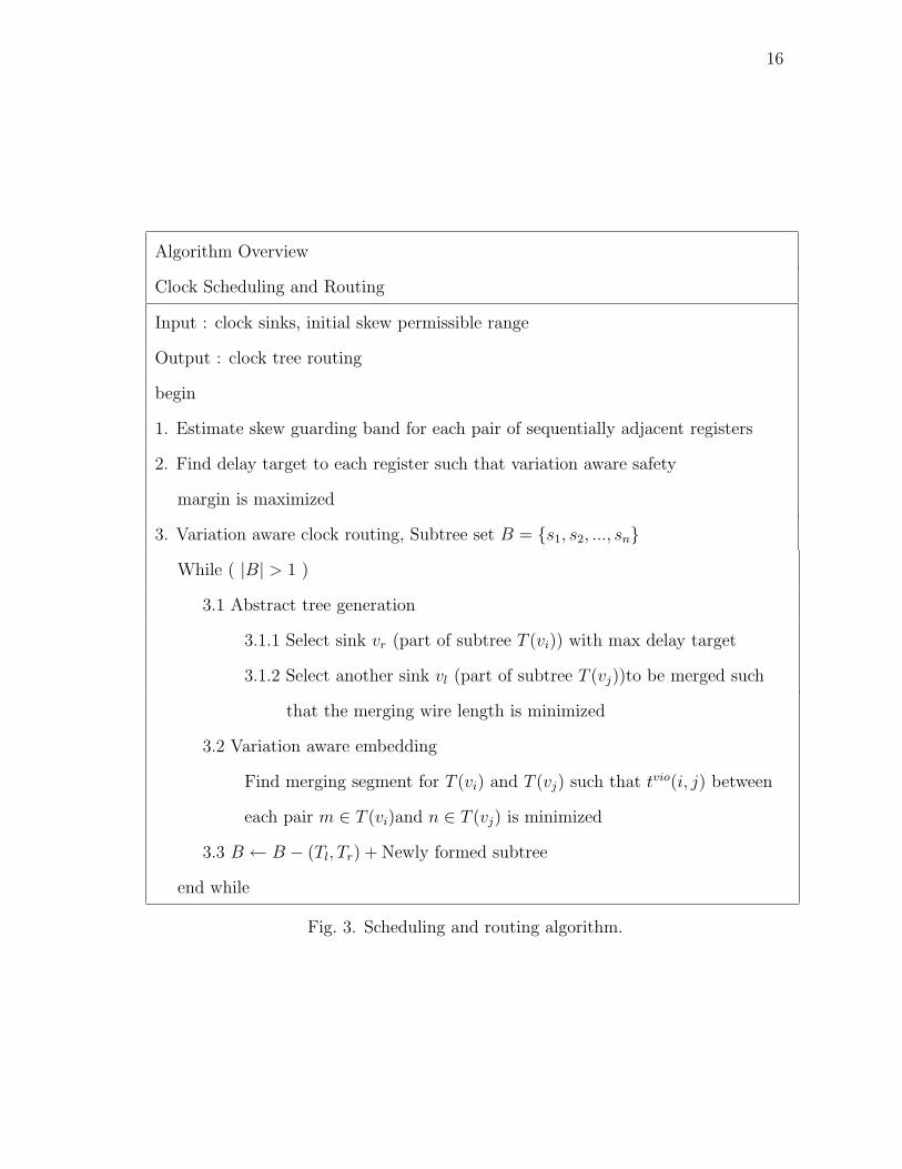
16
Algorithm Overview
Clock Scheduling and Routing
Input : clock sinks, initial skew permissible range
Output : clock tree routing
begin
1. Estimate skew guarding band for each pair of sequentially adjacent registers
2. Find delay target to each register such that variation aware safety
margin is maximized
3. Variation aware clock routing, Subtree set B = s1, s2, ..., sn
While ( |B| > 1 )
3.1 Abstract tree generation
3.1.1 Select sink vr (part of subtree T (vi)) with max delay target
3.1.2 Select another sink vl (part of subtree T (vj))to be merged such
that the merging wire length is minimized
3.2 Variation aware embedding
Find merging segment for T (vi) and T (vj) such that tvio(i, j) between
each pair m ∈ T (vi)and n ∈ T (vj) is minimized
3.3 B ← B − (Tl, Tr) + Newly formed subtree
end while
Fig. 3. Scheduling and routing algorithm.

17
2. Process Variation Aware Skew Scheduling
In skew scheduling, delay target ti to each register i is determined while the permis-
sible range as defined by Equation (2.1) is satisfied. In order to improve tolerance
to process variations, the skew safety margin min(tu(i, j) − tij, tij − tl(i, j)) needs
to be maximized for each pair of sequentially adjacent registers. Since the distance
between each pair of registers may be different from each other, the skew variation
for each pair is usually different from each other as well. Therefore, different amount
of safety margin should be allocated for different register pairs. The objective of our
skew scheduling scheme is to maximize skew safety margin with consideration of skew
variation between registers. If the estimated skew variation between register i and j
is δij, we formulate the scheduling problem as:
Maximize M (2.3)
∀ seq adj reg i and j
M ≤ tu(i, j)− δij − (ti − tj)
M ≤ (ti − tj)− tl(i, j)− δij
where M is the shared safety margin for each pair. This formulation may allocate
safety margins according to anticipated variation effect instead of uniform allocation
in previous works [1, 23, 24]. This linear programming problem can be solved by the
binary search method introduced in [19].
The estimated skew variation is obtained based on distance between registers
since the clock routing information is not available in the scheduling stage. For two
registers i and j, we assume they are merged at the middle point between them and
use the skew variation from this merging as an estimation. A wire segment of length
l driving a load of Cl has delay of 12rcl2 + rl
wCL. If wire width w varies around nominal

18
value w0 with bound of w0 ± dw and sink load varies as CLi = C0Li ± dCLi, the skew
variation between i and j is estimated to be:
δij =Dijr
2w0
(dCLi +CLi · dw
w0
+ dCLj +CLj · dw
w0
) (2.4)
where Dij is the Manhattan distance between register i and j. Even though this
estimation is an approximation, it reflects the trend that variability may grow with
distance.
3. Process Variation Aware Layout Embedding
In this section, we detail a layout embedding scheme that aims to minimize the max-
imum violation in skew due to process variation. Process variation aware embedding
was handled in [14], where a heuristic was used to identify a single critical pair and the
layout embedding focused on this pair alone. In our work, we propose a formulation
that considers the effect due to variation in all pairs.
Consider two subtrees T (vi) and T (vj) to be merged. In our approach, we shall
show that there exists a locus of points that has fixed distances from merging segments
ms(vi) and ms(vj) such that it minimizes the maximum skew violation. Maximum
skew violation is defined as the maximum deviation of the skew from its allowed
bounds among all sequentially adjacent register pairs. Let T viomax denote the maximum
skew violation. Then:
T viomax = max
(i,j)(tl(i, j)− tij, tij − tu(i, j)) (2.5)
Ideally, we would like T viomax to be negative implying that there is no violation. We
first formally state the problem that is addressed in this section.
Process variation aware layout embedding
Given two subtrees T (vi) and T (vj) to be merged, find a parent merging segment

19
ms(vij) such that the maximum skew violation among all sequentially adjacent pairs
(sr, sl) where sr ∈ T (vi) and sl ∈ T (vj) is minimized.
The above problem can also be formulated mathematically as described below.
For sr ∈ T (vi) and sl ∈ T (vj), let trl(evi, evj
) (trl(evi, evj
)) denote the maximum (min-
imum) skew between sr and sl due to process variation. Let trl denote the nominal
skew value. We intend to minimize the maximum skew violation, or equivalently
maximize the minimum difference between the skew bounds and the worst case skew
among all pairs. This is similar to the scheduling described in Equation (2.3) and can
be written as:
Maximize Sij (2.6)
∀ r ∈ T (vi) and l ∈ T (vj)
Sij ≤ tu(r, l)− trl(evi, evj
)
Sij ≤ trl(evi, evj
)− tl(r, l)
where Sij is a variable similar to the safety margin in skew scheduling. Maximizing
Sij is equivalent to minimizing skew violation.
The procedure to evaluate trl(evi, evj
) and trl(evi, evj
) under variation in wire-
width and load capacitances was detailed in [14]. We shall state it in brief and show
how formulation (2.6) can be transformed into a mathematical programming problem
with quadratic constraints. We also outline a technique which can be used to solve
this problem. Though we concentrate on wire-width and load capacitance variations,
the formulation given in (2.6) is generic and can be easily modified to take care of
other variations as well.
(tr, tr, tr) denote the minimum, nominal and maximum delays from sr (which is
part of the subtree T (vi)) to the node vi. (C li , Ci, C
ui ) represent the minimum, nom-

20
inal and maximum downstream capacitances at node vi respectively. Let αli(α
ui ) =
rCl
i
Wu(r
Cui
Wl) and φ = 1
2rc. Then:
trl(evi, evj
) = (tr + φe2vi
+ αui evi
)− (tl + φe2vj
+ αljevj
) (2.7)
Wu and Wl denote the bounds on the wire width. Interested reader may refer to [14]
for detailed derivation of the these equations.
Similarly trl(evi, evj
) may be written as:
trl(evi, evj
) = (tr + φe2vi
+ αlievi
)− (tl + φe2vj
+ αuj evj
) (2.8)
We can transform the formulation (2.6) into a mathematical programming problem
using equations (2.7) and (2.8).
Maximize Sij (2.9)
∀ r ∈ T (vi) and l ∈ T (vj)
Sij ≤ (tu(r, l)− tr + tl)− φ(e2vi− e2
vj)− (αu
i evi− αl
jevj)
Sij ≤ (−tl(r, l)− tl + tr) + φ(e2vi− e2
vj) + (αl
ievi− αu
j evj)
evi, evj≥ 0 evi
+ evj≥ Dij
The above formulation is quite different from the work in [14] where a single pair
of critical sinks were identified. After this, embedding was done in such a way that
the center of the worst case skew matches with the center of the permissible range.
However, this is a heuristic and there could be other pairs (other than the critical one)
which could face a significant deviation in skew due to process variations. Formula-
tion (2.6) attempts to overcome this difficulty. The parent merging segment cannot
exist if (evi+ evj
< Dij) and the final constraint takes care of that. The formulation
appears to be a difficult one to solve because of the presence of quadratic constraints.
21
But, we can consider two separate cases: case 1 does not require any wire snaking
and case 2 requires wire snaking. In each of these cases, the formulation can be trans-
formed in to another one with linear constraints. The method to identify the need
for wire snaking has been presented in [14].
Case 1: No wire snaking
In this case, evi+ evj
= Dij. Define the following parameters:
m1(r, l) = (tu(r, l)− tr + tl) + φD2ij + αl
jDij (2.10)
m2(r, l) = (−tl(r, l)− tl + tr)− φD2ij − αu
j Dij
k1 = 2φDij + αui + αl
j, k2 = 2φDij + αuj + αl
i
With no snaking formulation (2.9) gets modified in to the following linear program-
ming problem with just one variable:
Maximize Sij (2.11)
∀ r ∈ T (vi) and l ∈ T (vj), Sij ≤ m1(r, l)− k1evi
Sij ≤ m2(r, l) + k2evi, evi
≥ 0
Notice that the constraints in (2.11) represent straight lines with a positive slope of
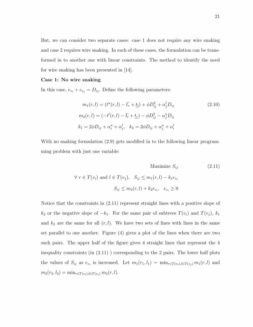
k2 or the negative slope of −k1. For the same pair of subtrees T (vi) and T (vj), k1
and k2 are the same for all (r, l). We have two sets of lines with lines in the same
set parallel to one another. Figure (4) gives a plot of the lines when there are two
such pairs. The upper half of the figure gives 4 straight lines that represent the 4
inequality constraints (in (2.11) ) corresponding to the 2 pairs. The lower half plots
the values of Sij as eviis increased. Let m1(r1, l1) = minr∈T (vi),l∈T (vj) m1(r, l) and
m2(r2, l2) = minr∈T (vi),l∈T (vj) m2(r, l).

22
Lemma 1
If no snaking is required, that is 0 ≤ evi, evj≤ Dij, then the optimal solution to (2.11)
exists at a point
evi=
m1(r1, l1)−m2(r2, l2)
k1 + k2
(2.12)
The proof is Lemma 1 is straightforward and Figure (3) gives the geometric intuition
behind the proof.
Case 2: With wire snaking
Wire snaking could mean either (evi= 0, evj
> Dij) or (evi= 0, evj
> Dij). We
discuss the latter and the equations can be modified to fit the former. Let m′
1(r, l) =
(tu(r, l) − tr + tl) and m′
2(r, l) = (−tl(r, l) − tl + tr). When we substitute evi= 0 in
formulation (2.9) we get:
Maximize Sij (2.13)
∀ r ∈ T (vi) and l ∈ T (vj)
Sij ≤ m′
1(r, l) + φe2vj
+ αljevj
Sij ≤ m′
2(r, l)− φe2vj− αu
j evj, evj
≥ 0
The optimal solution for (2.13) is obtained in a manner similar to that discussed for
case 1. Here, we have non-linear terms. But still the coefficients of evjand e2
vjare
the same for all (r, l). Let m1′(r1, l1) = minr∈T (vi),l∈T (vj) m
′
1(r, l) and m2′(r2, l2) =
minr∈T (vi),l∈T (vj) m′
2(r, l).
Lemma 2
If wire snaking is required with evi= 0 and evj
> Dij, then the optimal solution to
(2.13) exists at a point evjthat satisfies the following equation:
m′
1(r1, l1) + φe2vj
+ αljevj
= m′
2(r2, l2)− φe2vj− αu
j evj(2.14)

23
m (r ,l )
m (r ,l )
m (r ,l )
m (r ,l )
2 21
1 1 1
2 1 1
2 2 2
ev
evi
i
ij
Optimal Point
2 21 i
1 1 1 i
2 1 1 2
2 2 2
m (r , l ) - k ev
m (r , l ) - k ev
2m (r , l ) + k evm (r , l ) + k ev
i
i
1
1
S
Fig. 4. Plot of Sij with two pairs.
4. Alternative Layout Embedding
An alternative embedding procedure was also performed to make a comparison with
our proposed scheme. This method closely follows [14] with a key difference. In
[14], one critical pair was selected using a weighted function that considers both the
physical distance as well as the permissible range. Here we consider the feasible skew
range (FSR) [7] instead of the permissible range. The FSR matrix is updated after
every merge operation. After such an update, it is possible that the feasible skew
range of two sinks (say sr and sl) gets reduced. Interested reader may refer to [7] for
a detailed description of the FSR matrix and the process used to update it after every
merge. In such a scenario, we reduce the range by an additional factor (δrl) whose
value equals the difference between the maximum and the nominal skew multiplied

24
by a scaling factor. This way, we have an incremental scheduling scheme that reflects
the effect due to process variation.
5. Abstract Tree Generation
We first select a sink node (sa in a subtree rooted at vi) which has the maxi-
mum delay target. The second node is selected based on basis of expected wire
length added. Consider a sink node sb in a subtree rooted at (vj). We compute
the values of eviand evj
by the following procedure. To compute the actual val-
ues of eviand evj
, we first need to find two sink pairs (r1, l1) and (r2, l2) such that
m1(r1, l1) = minr∈T (vi),l∈T (vj) m1(r, l) and m2(r2, l2) = minr∈T (vi),l∈T (vj) m2(r, l). This
could be prohibitively expensive for all pairs. So we use the heuristic where we assign
(r1, l1) = (r2, l2) = (a, b). Then by using the procedure detailed earlier, we iden-
tify the need for snaking and use equation (2.12) or (2.14) to compute eviand evj
.
This serves as the merging cost. We claim that such a heuristic performs better and
have experimental results to support the claim. This procedure will be referred to as
embedding aware abstract topology construction.
6. Algorithm Complexity
The complexity of the process variation aware scheduling is O(nm) where n is the
number of sinks and m is the number of constraints for the linear programming
formulation. The complexity of each embedding is O(n) and the total run time for
O(n) embeddings is O(n2). Even though m = O(n2) in theory, in practice m = O(n).
Therefore, the overall complexity of our algorithm is O(n2).

25
E. Experimental Results
The proposed procedure was tested on five benchmark circuits [18]. The values of
the technology parameters used were obtained from [14]. The benchmark circuits do
not contain the timing information (permissible range for each sink pair). So, we
generated the permissible ranges randomly such that for every (sr, sl), tl(r, l) < 0 <
tu(r, l). The permissible ranges were not symmetric but chosen such that ||tu(r, l)| −
|tl(r, l)|| < 100ps, tl(r, l) ∈ (−600ps,−100ps) and tu(r, l) ∈ (100ps, 600ps). The code
was written in C and run on a Sun Solaris Ultra Sparc machine with 2 GB RAM.
We ran our experiments for five methods (based on scheduling, topology and
embedding) denoted as:
• BASE CASE: No scheduling, topology based on distance, embedding follows [14]
• SP-DISTANCE: Process variation aware scheduling, topology based on dis-
tance, embedding follows [14]
• MP-DISTANCE: Process variation aware scheduling, topology based on dis-
tance, the new embedding scheme
• SP-eAWARE: Process variation aware scheduling and topology, embedding fol-
lows [14]
• MP-eAWARE: Process variation aware scheduling and topology, the new em-
bedding scheme
In the above mentioned methods, BASE CASE is almost similar to [14] and MP-
eAWARE represents our complete solution proposed. Experiments were run on the
remaining three methods to show the effect of each individual technique, thereby
providing a better insight. Monte Carlo simulations (1000 runs) were done for all

26
Table I. Results for the base case.
Case #Sinks BASE CASE
WL #Vio Max Vio CPU
r1 267 1.97 0.21 3.43 00:01
r2 598 3.85 18.60 69.91 00:06
r3 862 4.59 33.37 88.52 00:13
r4 1903 9.53 553.39 573.64 00:51
r5 3101 14.39 1523.30 1392.39 02:31
five methods. In each run, the wire width and load capacitance were chosen at ran-
dom from a uniform distribution with mean being the nominal value and standard
deviation set such that 3σ corresponds to 10% deviation from the nominal value.
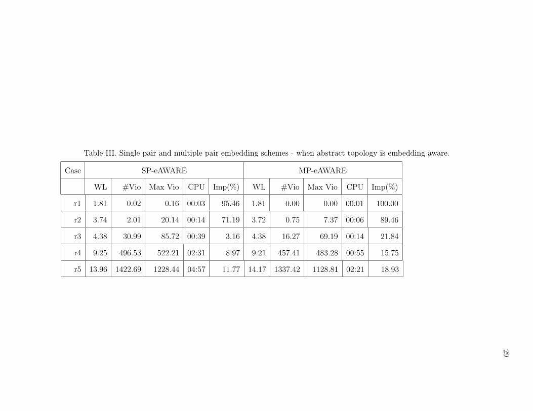
Table (I) shows the results for BASE CASE, Table (II) for SP-DISTANCE and MP-
DISTANCE, Table (III) for SP-eAWARE and MP-eAWARE. The sub columns repre-
sent wire length (WL) (in 1e+6µm), Number of violations (#Vio), average maximum
violation in ps (Max Vio) CPU (in min:sec) and Improvement (of maximum violation
in percentage compared to the base).
As it is evident from the Table (III) there is a significant difference in the maxi-
mum skew violation between our proposed scheme and the base case. Moreover (MP-
DISTANCE, MP-eAWARE) perform better than (SP-DISTANCE, SP-eAWARE)
highlighting the effectiveness of our embedding technique. Our primary focus is to
reduce the maximum skew violation and not number of violations since the former
has a greater impact on the choice of the clock frequency. For example consider two
scenarios: case (a) 50 violations with a maximum violation of 25 ps and case (b) 1
violation of 50 ps. Case (a) could be handled by slowing the clock by 25 ps whereas

27
case (b) would require a reduction of 50 ps in clock speed. Nevertheless, proposed
technique results in a significant gain in the number of violations as well.

28
Table II. Single pair and multiple pair embedding schemes - when abstract topology is distance based.
Case SP-DISTANCE MP-DISTANCE
WL #Vio Max Vio CPU Imp(%) WL #Vio Max Vio CPU Imp(%)
r1 1.87 0.01 0.07 00:03 98.11 1.83 0.00 0.00 00:01 99.85
r2 3.84 6.98 42.57 00:16 39.11 3.80 2.93 17.80 00:06 74.54
r3 4.39 27.55 93.87 00:40 -6.04 4.37 15.95 58.73 00:14 33.65
r4 9.25 516.73 544.63 02:40 5.07 9.33 521.49 488.19 00:56 14.90
r5 14.37 1491.21 1383.35 05:09 0.65 14.44 1474.21 1251.36 02:20 10.13
29
Table III. Single pair and multiple pair embedding schemes - when abstract topology is embedding aware.
Case SP-eAWARE MP-eAWARE
WL #Vio Max Vio CPU Imp(%) WL #Vio Max Vio CPU Imp(%)
r1 1.81 0.02 0.16 00:03 95.46 1.81 0.00 0.00 00:01 100.00
r2 3.74 2.01 20.14 00:14 71.19 3.72 0.75 7.37 00:06 89.46
r3 4.38 30.99 85.72 00:39 3.16 4.38 16.27 69.19 00:14 21.84
r4 9.25 496.53 522.21 02:31 8.97 9.21 457.41 483.28 00:55 15.75
r5 13.96 1422.69 1228.44 04:57 11.77 14.17 1337.42 1128.81 02:21 18.93

30
CHAPTER III
LINK INSERTION IN BUFFERED CLOCK NETS
Link insertion consists of adding cross-links to an existing clock tree, thereby con-
verting it in to a non-tree. The primary objective of link insertion is to increase
the tolerance of the clock network to PVT variations. In this chapter, we address
the issues involved in inserting links in a buffered clock network. We analyze the
short-circuit risk involved in inserting cross links in a buffered tree. Based on this
analysis, we propose a design criteria to avoid the risk. Link insertion assumes a
zero skew tree as input. We detail a skew tuning technique that produces low skew
trees. In the experimental section, we compare the variation and power results of our
approach with clock trees as well as clock mesh (a popular form of non-tree based
clock distribution).
A. Preliminaries
The following notations/conventions will be followed in this chapter:
• S = s1, s2, ...sn denotes the set of clock sinks.
• The capacitance of an interconnect of length l is given by c · l, where c denotes
the capacitance per unit length.
• The resistance of an interconnect of length l is given by r · l where r denotes
the resistance per unit length.
• For initial tree construction, we use linear delay model for the buffers. The
delay of a buffer is given by:
tbuf = rbCload + tb (3.1)

31
In the above equation rb denotes the resistance and tb the intrinsic delay of the
buffer. Cload denotes the load driven by the inverter.
• SPICE simulations refer to simulations using HSPICE unless otherwise speci-
fied.
B. Previous Work
We summarize a few important conclusions from previous work on link insertion [8].
The basic idea behind the link based non-tree clock network construction is to obtain
a non-tree by inserting cross links between nodes in an existing clock tree. A link can
be modeled as a link resistor with a pair of link capacitors at the two ends. Adding
only link capacitances to a clock tree may change the skew but does not change the
tree topology. The original skew can be restored by tuning the tree as in conventional
clock tree routing methods.
If a link resistor is inserted between a pair of nodes with equal nominal delay
(or zero nominal skew), there is no change on nominal delay at any node in the clock
network. If there is skew variation between the two end nodes of the link resistor, the
magnitude of the variation is always scaled down by the link resistance. The effect of
the scaling is strong when the link resistance is small or the nearest common ancestor
node of the two end nodes is close to the root. If one end of the link is in subtree
Tl and the other end is in a disjoint subtree Tr, the link resistance can reduce skew
variation between any pair of nodes of Tl and Tr. However, the link resistance may
worsen skew variability between nodes in some other circumstances (see [8]). The
major guidelines for link insertions include:
• Links are always inserted between nodes with zero nominal skew.
• Links are preferentially inserted between node pairs which are close to each

32
other and their nearest common ancestor node is close to the root in the abstract
topology.
• Links need to be distributed evenly in the clock network so that their skew
worsening effects can cancel each other.
The main advantage of link insertion is that it provides a good trade off between
skew reduction and increase in wire length. Compared to clock trees, cross link inser-
tion can reduce the maximum skew variation by over 30% with less than 2% increase
in wirelength [8]. A clock mesh can reduce the maximum skew variation by 90% but
with over 60% increase in wirelength [8]. Therefore, a link based non-tree approach is
an appealing choice for many ASIC designs which have relatively stringent cost/power
constraints. Since such non-trees are built upon existing clock trees, this method can
be easily incorporated with traditional tree based design methodology. Moreover, it
can be easily extended to achieve useful non-zero clock skews. The relatively difficult
non-tree delay computation is circumvented in the methods introduced in [8]. The
link insertion in [25] is a special case which handles only H-trees.
Despite the advantages, previous works on link based non-tree clock network [8, 9]
have a few shortcomings which hamper their applicability. The major weakness is
that these works [8, 9] are limited to unbuffered clock networks. In reality, most clock
networks are buffered due to the requirements on signal slew rate and maximum path
delay. More importantly, buffer variations [26, 27] are usually the major contributors
to clock skew variations. The effect of link insertion in buffered networks is more
difficult to control than that in unbuffered cases due to the nonlinear behavior of buffer
delays and the appearance of multi-driver nets. In addition to this methodological
weakness, the experimental setup of [8, 9] neglected spatial correlations [28, 29] in
the variation models. It has been recognized that many variations such as intra-

33
die process variations [29] and power supply fluctuations are spatially correlated.
Link insertion for buffered clock nets was also handled in [30] (published after the
preliminary version [31] of this work). We differ from [30] in the following aspects.
1. Our work addresses the issue of multi-driver nets - which is a key concern while
inserting links in buffered clock nets.
2. In the experimental results section, we quantify the impact of link insertion on
power dissipation.
3. We compare the results from link insertion (wire length, skew variation and
power dissipation) with that of clock mesh - a popular form of non-tree based
clock distribution.
C. Problem Statement
Link Insertion for Buffered Clock Networks
Given a set of clock sinks S = s1, s2, ...sn, and their load capacitances (a) construct
a zero skew buffered clock tree and (b) Insert links in this clock tree such that (i) The
risk of short-circuit current is avoided (ii) The tolerance of the clock net to variations
in clock skew is improved and (iii) The increase in wire length/ power dissipation is
minimized.
D. Multi-driver Nets
If cross links are inserted in a buffered clock network, it is likely that a sub-net is
driven by multiple buffers or drivers. This fact causes two issues which do not exist in
link insertion for unbuffered clock networks. One is the risk of short circuit between
the outputs of different buffers. The other is whether or not the analysis on delay

34
and skew in [8] is still valid in the multi-driver nets.
1. Short Circuit Avoidance
If the signal arrival times at the inputs of two buffers driving the same sub-net are
significantly different, there is a risk of short circuit power consumption. This arrival
time difference can be caused by either nominal delay difference or delay variations.
Consider the example in Figure (5) where the outputs of the two buffers are initially
low and then switch to high with time difference ∆. There is an time interval ∆
during which the output of upper buffer is high while the output of the lower buffer is
low. Therefore, there could be a short circuit current flowing from the power supply
to the ground through the upper buffer and then the lower buffer as indicated by the
dashed line in Figure (5).
∆
Link
Fig. 5. If there is significant difference ∆ between signal arrival time to the two drivers,
there is risk of short circuit indicated by the dashed line.
However, the signal propagates with a finite time delay from one buffer to an-
other. If this delay is greater than ∆, then there is not enough time to establish the
short circuit current. In other words, the output of the lower buffer may switch to
high before the signal of the upper buffer propagates to it. Based on this observation,
a design criterion for avoiding short circuit current between two buffers is derived as
35
follows.
Denote the two buffers as Bi and Bj. Let the upper bound of the difference
between signal arrival time to Bi and Bj be ∆ij,max considering variations. The lower
bound τi7−→j of signal propagation delay from Bi to Bj can be obtained through the
method detailed in [16, 32].
τi7−→j =
∑
(u,v)∈path(Bi 7−→Bj) R2uvCv
∑
(u,v)∈path(Bi 7−→Bj) Ruv
(3.2)
where (u, v) indicates two end nodes of an edge, Ruv is the edge resistance and Cv
is the total capacitance downstream of node v. The lower bound τj 7−→i of signal
propagation delay from Bj to Bi can be obtained similarly. Then, the criterion for
avoiding short circuit between Bi and Bj is:
min(τi7−→j, τj 7−→i) > α∆ij,max (3.3)
where α > 1 is a constant used for added safety margin.
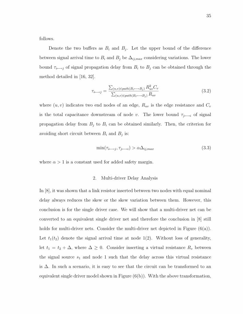
2. Multi-driver Delay Analysis
In [8], it was shown that a link resistor inserted between two nodes with equal nominal
delay always reduces the skew or the skew variation between them. However, this
conclusion is for the single driver case. We will show that a multi-driver net can be
converted to an equivalent single driver net and therefore the conclusion in [8] still
holds for multi-driver nets. Consider the multi-driver net depicted in Figure (6(a)).
Let t1(t2) denote the signal arrival time at node 1(2). Without loss of generality,
let t1 = t2 + ∆, where ∆ ≥ 0. Consider inserting a virtual resistance Rv between
the signal source s1 and node 1 such that the delay across this virtual resistance
is ∆. In such a scenario, it is easy to see that the circuit can be transformed to an
equivalent single driver model shown in Figure (6(b)). With the above transformation,

36
ii
Rd1 Rd1
Rd2Rd2
(a)
s1
1
2
1
2
s2s2
Rv
(b)
Fig. 6. The dual driver net in (a) can be converted to the single driver net in (b) when
signal departure time t1 at node 1 is no less than the signal departure time t2
at node 2.
the analysis detailed in [8] still holds good. Since inserting a link between two equal
delay nodes does not affect the delay at any node, the delay across Rv can be obtained
by ripping up all of the link resistance and finding the Elmore delay in the resulting
tree. Therefore, the value of Rv is equal to ∆C1
where C1 is the total downstream
capacitance at node 1 for the tree.
E. Localized Skew Tuning
For link insertion to be effective, we need to insert links between nodes with zero
nominal skew [8]. However, generation of a low nominal skew tree (under a higher
order delay model) is non-trivial. We will illustrate this difficulty through an example
of zero skew clock tree construction in Figure (7). If zero skew has already been
obtained for the buffered subtrees rooted at a1 and a2, we attempt to tune the
location of the merging node m3 such that the delay from m3 to each sink (s1, s2,
s3 or s4) is the same. Let downstream delay at a node k, or the delay from k to
sinks, be denoted as dk. The location of m3 is decided based on downstream delay
da1 = delay(B1) + dm1 and da2 = delay(B2) + dm2. The buffer delays delay(B1) and

37
m3 location
buffer delay
downstream delay input slewB1
a1 a2
B2
s3s2s1
m1 m2
s4
m3
Fig. 7. Tuning the location of merging node m3 in a buffered clock tree falls into a
cyclic dependency.
delay(B2) depend on their input slew rates. However, the input slew rates depend
on the location of merging node m3. We thus get into a vicious cycle that makes it
very difficult to accurately find a merging node location that gives zero skew. This
cycle is depicted at the right part of Figure (7).
The weakest link in this cycle is the dependence of merging node location on the
downstream delay da1 and da2. Tunable delay elements were discussed in [33] as a
technique used to improve the post-silicon yield. We employ this technique to break
the weakest link as well as the vicious cycle. If buffer delay delay(B1) and delay(B2)
can be tuned without affecting other delay or slew in the buffered tree, we can decide
the location of m3 regardless downstream delay da1 and da2 and then obtain zero skew
at sinks by tuning the buffer delays. Figure (8) shows an example of a tunable buffer
containing three cascaded inverters even though different number of inverters can be
employed. There is a tunable dummy capacitor C between inverter I1 and inverter I2.
For a given input slew and a given output load, the delay of the buffer can be tuned
by sizing the dummy capacitor. Since the dummy capacitor is sandwiched between
inverters in the buffer, changing its size does not affect any other delay or slew in the
buffered tree but the buffer delay itself. In contrast to post-silicon tuning in [33], the
tuning in our case is performed during the clock network layout and therefore does

38
not involve any testing cost.
C
I1 I2 I3
Fig. 8. Tunable clock buffer.
F. Link Based Buffered Clock Network Construction
1. Buffered Clock Tree Construction
The link based non-tree clock network construction starts with an initial buffered
clock tree. There are many previous works on clock tree routing [17, 20] and buffered
clock tree construction [34, 35, 36, 37] and various techniques are included in these
different works. We integrate the best of them, those friendly to link insertion and
the tuning technique (Section E) into a method to construct buffered clock trees.
We show that the techniques are integrated in such a manner that facilitates link
insertion.
Similar to previous works [34, 35, 36], we try to build a balanced tree with
equal number of buffers along every source-sink path. This balanced buffered clock
tree scheme is illustrated in Figure (9). Such balanced structure itself has certain
tolerance to inter-die variations [34, 35]. Further, we will show later that it is friendly
to link insertion.
The buffered clock tree is constructed through a bottom-up merging procedure
like many traditional clock routing algorithms [17, 20, 37]. The merging order is
based on the nearest neighbor method [20] which selects a pair of subtrees closest to

39
level i
level i+1
p
v
wu
r2 r3 r4r1k
l r
l2 l4l3l1
Nearest common ancestor
Fig. 9. Link insertion in buffered clock tree. Dashed lines indicate links.
each other for merging. In order to maintain the tree balance, we impose an extra
restriction that only subtrees with fewer levels are merged first. The location of each
merging node is decided by the DME (Deferred Merge Embedding) technique [17]
based on the Elmore delay model. Buffers are inserted at every internal node at
the same level as in Figure (9) such that the maximum load of each buffer/driver is
limited. This is an indirect way to ensure proper signal slew rate [37].
In addition to the structural balance, we perform delay balancing [34] for
subtrees at each level. After the buffer insertions, the entire tree can be partitioned
into subtrees at different levels indicated by the dotted lines in Figure (9). In delay
balancing, we make the delay of subtrees at the same level identical. For example,
delay(l 7−→ u) = delay(r 7−→ w) for Figure 9. The delay balancing can be achieved
by using the tunable buffer detailed in Section E and sizing the dummy capacitors.
Delay balancing has several advantages. First, delay balancing results in almost
equal signal arrival time at each buffer of the same level. Hence, the risk of short
circuit is greatly reduced if link insertion is restricted among subtrees of the same level
40
according to the discussions in Section 1. The other reason is for the convenience of
multilevel link insertion. Every subtree rooted at a buffer/driver becomes a zero
skew subtree after delay balancing. Then, cross links can be easily inserted between
subtrees at higher levels like the link between u and w in Figure 9. Further, as it will
be explained in detail in section 2, delay balancing could lead to significant reduction
in wire length.
After the buffered clock tree is constructed, a SPICE simulation is performed to
obtain a precise estimation on clock skew. Usually, the skew within a subtree rooted
at a buffer/driver is negligible. Since there is no buffers within such a subtree, the
Elmore model provides a fairly good fidelity which is verified by SPICE simulations in
[9]. However, there could be a significant delay difference between different subtrees
at the same level. Thus, we perform a post-processing of delay balancing through
tuning the clock buffers based on the SPICE based skew information. Compared to
previous skew tuning work [38] using SPICE model, our method is much easier.
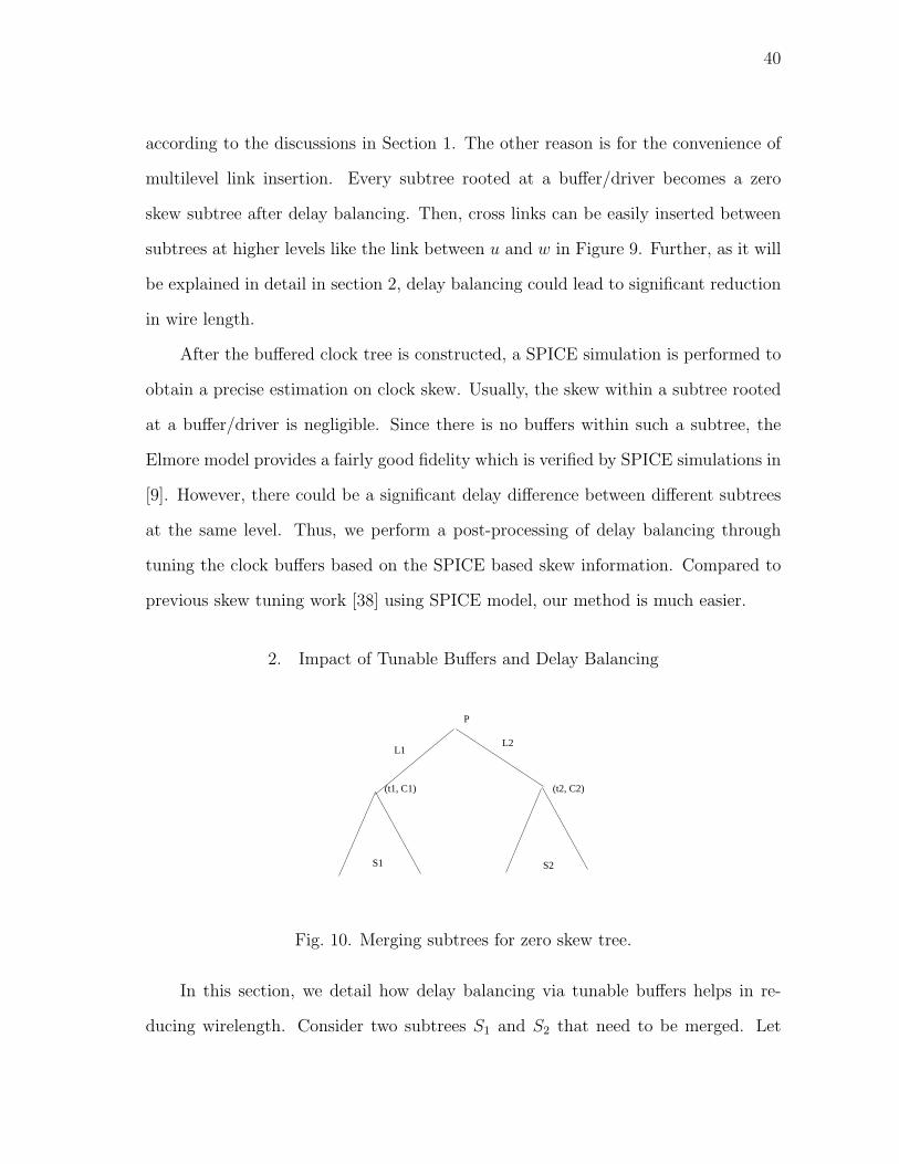
2. Impact of Tunable Buffers and Delay Balancing
(t1, C1) (t2, C2)
P
L1L2
S1 S2
Fig. 10. Merging subtrees for zero skew tree.
In this section, we detail how delay balancing via tunable buffers helps in re-
ducing wirelength. Consider two subtrees S1 and S2 that need to be merged. Let

41
t1 (t2) and C1 (C2) denote the downstream delay and capacitance at the root of S1
(S2) respectively. Let r and c denote the per-unit resistance and capacitance of the
interconnect. The subtree characteristics are illustrated in Figure 10. Let L1 and L2
denote the distances between the merging point and the root of the subtrees S1 and
S2 respectively. Let L denote the distance between the root of the subtrees. In order
to achieve zero skew, the lengths should satisfy [18].
L1 = L(t2 − t1) + rL(C2 + cL
2)
rL(cL + C1 + C2)(3.4)
L2 = L− L1
The above equations are valid when 0 ≤ L1, L2 ≤ L. If t1 >> t2, it is possible that
L2 > L. In such a case (and the converse where L1 > L) we need to assign L1 = 0
and L2 > L. This scenario is also known as wire snaking. If wire snaking is required
with L2 > L, L2 can be computed using the following formula [18]:
L2 =
√
(rC1)2 + 2rc(t2 − t1)− rC1
rc(3.5)
Notice that, in case there is no snaking, the extra wirelength added as a result of
merging the two subtrees equals L. With snaking, let Lsnaking denote the snaking
length defined as L2 − L. In other words:
Lsnaking = (
√
(rC1)2 + 2rc(t2 − t1)− rC1
rc)− L (3.6)
In case of delay balancing, we make sure that the subtrees to be merged have equal
delays (or t1 = t2. This implies that L1 = L2 = L2
or there is no snaking. Delay
balancing is achieved via adding an extra capacitance between inverters I1 and I2 in
the inverter chain (Figure 8). Let the delay of inverter I1 be characterized by the

42
following equation:
tinv = rbCload + tb (3.7)
In the above equation rb, Cload and tb denote the output resistance, load capacitance
and intrinsic delay of the inverter respectively. Hence, the length of the capacitance
that needs to be added for delay balancing equals:
lbalance =(t1 − t2)
rbc(3.8)
Hence, lbalance would be the extra wirelength spent on delay balancing. Table IV
shows the comparison between delay balancing and traditional wire snaking for some
typical values of subtree delay differences. The first column denotes the difference
between the downstream delays of the two subtrees in psec. The second and third
columns denote the values of Lsnaking and lbalance in µm respectively. The final column
denotes the ratio of lbalance to Lsnaking. The downstream capacitances of the subtrees
were set to 0.2 and 0.1 pF respectively. The distance between the subtrees (L) was
set to 50 µm, the per unit capacitance and resistance were set to 0.39Ω/µm and
1.55fF/µm respectively (parameters taken out of 65nm process [39]). The chain of
inverters (I1, I2, I3) were sized at 5x, 15x and 45x times the size of the minimum size
inverters in the 65nm process. The value of rb was found to be 2224.6Ω using HSPICE
simulations on a 5x size inverter using 65nm model cards from BPTM [40]. It can
be seen from Table IV that delay balancing tend to consume far lesser wirelength as
compared to traditional wire snaking. This is mainly due to the fact that rb >> r
(rb is large since the first inverter in the chain is the smallest). Experimental results
on the clock benchmarks indicate that delay balancing results in 46% reduction in
wirelength and 54% reduction in skew on an average.

43
Table IV. Comparison between snaking and delay balancing.
(t1 − t2) Lsnaking lbalance Ratio
5.0 2542.8 14.5 0.01
10.0 2567.8 29 0.01
20.0 2617.2 58 0.02
30.0 2665.9 87 0.03
40.0 2713.9 116 0.04
3. Link Insertion
The algorithm for link insertion in buffered clock networks has some significant differ-
ences from the unbuffered case [8, 9], although they share the same top-level frame-
work illustrated below.
1. Select the node pairs for link insertion.
2. Add link capacitance to the selected nodes and perform skew tuning to restore
the original skew. The skew tuning includes two steps. First, the locations of
merging nodes in each subtree rooted at a buffer/driver are tuned to restore
zero skew for the subtree. Next, SPICE simulation is performed to obtain a
precise inter-subtree skew estimation. And the inter-subtree skew is minimized
by sizing the dummy capacitors in the tunable clock buffers. This step is the
same as the post-processing in the initial buffered clock tree construction.
3. Insert link resistance into the selected node pairs. Since we always select node
pairs with zero nominal skew and restore such zero skew in skew tuning of
previous step, the link resistances do not affect nominal skew.

44
Procedure: NodePairsBetweenTrees(Tl, Tr,m)
Input: Two subtree Tl and Tr,
size indicator m for each sink/buffer level
Output: A set P of node pairs
1. P ← ∅
2. For each sink/buffer level deeper than l and r
3. Decompose Tl to sub-subtrees Sl = l1, l2...lm
4. Decompose Tr to sub-subtrees Sr = r1, r2...rm
5. Construct bipartite graph Gl,r between Sl and Sr
6. Gp ← MST of Gl,r
7. For each edge (li, rj) in Gp
8. If link between li and rj has short circuit risk
10. Remove (li, rj) from Gp
12. Else if weight(li, rj) > threshold
13. Remove (li, rj) from Gp
14. P ← P∪ edges in Gp
15. Return P
Fig. 11. Algorithm of selecting node pairs between two subtrees.

45
The most important step is node pair selection. Similar to [8, 9], the selection proceeds
from the root node toward the leaf nodes recursively. In Figure (9), when an internal
node p is visited during this tree traversal, node pairs between its left subtree Tl rooted
at node l and right subtree Tr rooted at r are selected. Every node pair between Tl
and Tr share the same nearest common ancestor node p. Then, the same procedure
is performed for nodes l, r and their child nodes. The algorithm for selection of
node pairs between Tl and Tr is shown in Figure (11). The input to this algorithm
is a user-specified parameter m which roughly indicates the number of pairs to be
selected.
The node pair selection procedure at each sink/buffer level is derived from the
MST (Minimum Spanning Tree) based algorithm in [9]. Both the left subtree Tl
and the right subtree Tr are decomposed into m sub-subtrees. In Figure (9), each
subtree is decomposed into 4 sub-subtrees. Then, a bipartite graph is generated with
each vertex corresponding to a sub-subtree. The weight of an edge is equal to the
minimum sink/buffer distance between the two sub-subtrees it is incident on. For
example, if the nearest sink pair between sub-subtree l3 and sub-subtree r2 is k and
v in Figure (9), the weight of edge (l3, r2) is equal to the distance between sink k and
sink v. Next, an MST (Minimum Spanning Tree) on this bipartite graph is obtained.
The edges in the MST correspond to candidate node pairs for the selection.
These candidate edges are further pruned through a rule based iterative deletion as
in line 7-13 of Figure 11. However, our algorithm differs from [9] by the fact that
we employ delay balancing at levels where buffers are inserted. Such a balancing
creates several pairs of zero skew nodes where a link could potentially be inserted. In
addition to [9], our algorithm considers one more criteria for edge deletion. This is
to ensure that there is no short circuit risk when a link is inserted for a node pair. If
the inequality (3.3) is violated, the corresponding edge is removed.

46
Since the bipartite graph has m vertices, the MST has 2m− 1 edges. Hence, the
number of node pairs selected for Tl and Tr at a sink/buffer level is on the order of
m.
G. Experiment
1. Experiment Setup
We use both the ISCAS89 benchmark suites as well as the well known r1− r5 bench-
marks [18] for our experiments. The ISCAS89 benchmark suites were synthesized
using SIS [41] and placed using mPL [42]. The interconnect parameters (per-unit
resistance and per-unit capacitance) were obtained from [39]. All buffers were char-
acterized (for buffer resistance and intrinsic delays) using 65nm model cards from
BPTM [40]. Our tunable buffer consists of a chain of three inverters of size 5x, 15x
and 45x times that of the minimum size inverter in the 65nm process. All simulations
were performed using HSPICE. The skew results presented (nominal as well as due
to due to variation) refers to the maximum skew among all clock sink pairs (in other
words the global skew) after running accurate simulation using HSPICE (since the
sequential adjacency information is not available for the benchmark circuits r1− r5,
we used the global skew as the metric).
Our techniques were implemented in C++ and run on a Linux Work station with
2GB RAM. Clock skew variations were evaluated through Monte Carlo simulations.
We consider the following sources for on-chip variations:
• Buffer channel length.
• Power supply voltage.
• Interconnect wire width variation.

47
• Sink load capacitance variation.
These variations are assumed to follow Gaussian distribution with standard deviations
equal to 5% (for power supply, we set it to 3% of the nominal value) of their nominal
values. Spatial correlations among the variations are handled by the PCA (Principle
Component Analysis) method as in [29]. Power dissipation was measured by accurate
HSPICE simulations. This includes all sources of power dissipation - dynamic, leakage
and short-circuit.
2. Experiment Design
In this work, we propose three different techniques, namely:
1. Delay balancing.
2. Skew tuning via tunable buffers.
3. Link insertion for buffered clock networks.
We need to evaluate the impact of the above three methods with respect to the
following design parameters:
1. Resource Consumption - consists of wire length (WL) and power dissipation.
2. Nominal Skew (NS) - the skew measured when all the parameters are set to
their ideal values (no variations).
3. Skew Due to Variations - the skew measured via Monte Carlo simulations.
In all the tables presented, the following conventions will be used unless otherwise
specified.
• WL denotes the wire length in µm.

48
• NS denotes the nominal skew. µskew, σskew and MSV denote the mean skew,
standard deviation of the skew, and the maximum skew among 1000 runs of
Monte Carlo. All skew results are reported in psec.
• Pow denotes the power dissipation in mW .
• BA denotes the buffer area in µm2.
• CPU time is reported in seconds.
• Imp denotes Improvement in %.
3. Experimental Results
We first explore the impact of delay balancing and skew tuning on resource consump-
tion and nominal skew. Table (V) gives the results for clock trees with no delay
balancing and no skew tuning. In other words, this table gives the results obtained
none of the techniques detailed on this work are used. The columns in Table (V)
denotes the test case name, number of clock sinks, wire length, # of buffers, buffer
area, power dissipation, Nominal Skew and the CPU time.
Table (VI) presents the results for clock trees with delay balancing and no tuning.
For each of the parameter, we also present the improvements as compared to the ones
obtained with clock trees without balancing (shown in Table V). It is evident that
delay balancing alone can improve the wire length by 46%, power by 35% and skew
by 54%. Since we pre-characterize the buffers, the CPU time is identical to the ones
when no delay balancing is done. This table gives the experimental validation for the
discussions presented in Section 2.
Table (VII) presents the results for clock trees with delay balancing and tuning.
For each of the parameter, we also present the improvements as compared to the ones

49
obtained with clock trees with balancing and without tuning. It may be noted that
using skew tuning, we can reduce the nominal skew by up to 33%. Since the wire
length increase is insignificant, we use the same number of buffers. Consequently,
there is no increase in area or power dissipation. The run time is determined by one
run of HSPICE on the clock tree which is also very reasonable.
Table (VIII) presents the variations results obtained by running Monte Carlo
simulations (1000 HSPICE runs) on clock trees obtained using delay balancing and
tuning. Since such a scheme gives the best clock tree, we use this as the base case for
comparison with non-trees (links and mesh). We present the mean (µskew), variance
(σskew) and the maximum (MSV) of the skew variations.
Table (IX) presents the variation and resource consumption results for link in-
sertion and compares it with clock trees. With link insertion, we could reduce the
maximum skew variation by over 32% with less than 5% increase in power dissi-
pation. Table (X) presents similar results for clock mesh. It may be noted that
clock mesh does have a better variation tolerance than links. However, the power
consumption of mesh is also quite high - more than 70% on an average.

50
Table V. Results for clock trees without delay balancing, without tuning.
No Balancing, No tuning
Case #Sinks WL #Buffers BA Pow NS CPU
s9234 135 8249 10 10.99 1.90 15.31 0.02
s5378 164 9681 12 13.18 2.31 10.97 0.04
r1 267 11470 22 24.17 3.57 5.19 0.08
r2 598 49607 114 125.23 17.25 57.48 0.94
r3 862 79351 155 170.27 22.45 67.51 3.10
r4 1903 173534 467 513.00 57.57 104.62 31.23
r5 3101 439896 1544 1696.08 166.32 50.43 138.00
Ave 879 110255 332 364.7 38.77 44.5 24.77

51
Table VI. Comparison between (delay balancing, no tuning) vs (no delay balancing, no tuning).
Balancing, No tuning
Case WL Imp Buffers Imp BA Imp Pow Imp NS Imp CPU
s9234 5202 36.94 8 20.00 8.79 20 1.20 37 3 80.40 0.02
s5378 6118 36.80 10 16.67 10.99 16.67 1.48 35.93 5.44 50.41 0.04
r1 6805 40.67 16 27.27 17.58 27.27 2.44 31.65 5.22 -0.58 0.08
r2 24737 50.13 83 27.19 91.18 27.19 10.47 39.30 15.03 73.85 0.94
r3 43178 45.59 123 20.65 135.12 20.65 16.25 27.62 34.00 49.64 3.10
r4 92701 46.58 279 40.26 306.48 40.26 35.87 37.69 28.93 72.35 31.23
r5 308887 29.78 949 38.54 1042.48 38.54 120.68 27.44 50.43 79.87 136.00
Ave 29687.50 46.33 86.50 25.34 95.02 25.34 11.28 34.87 15.27 54.35 5.90

52
Table VII. Comparison between (delay balancing, WITH tuning) vs (delay balancing WITHOUT tuning).
Balancing AND tuning
Case WL Imp Buffers Imp BA Imp NS Imp Pow Imp CPU
s9234 5202 0.00 8 0.00 520 0.00 3.00 0.00 1.20 0.00 0.61
s5378 6118 0.00 10 0.00 650 0.00 5.44 0.00 1.48 0.00 0.68
r1 6805 0.00 16 0.00 1040 0.00 5.22 0.00 2.44 0.00 1.25
r2 24737 -0.48 83 0.00 5395 0.00 7.98 46.91 10.47 0.00 7.98
r3 43178 -0.51 123 0.00 7995 0.00 11.93 64.91 16.25 0.00 14.32
r4 92701 -0.30 279 0.00 18135 0.00 12.36 57.28 35.87 0.00 82.79
r5 309614 -0.24 949 0.00 61685 0.00 18.81 62.7 120.68 0.00 137.00
Ave 69765 -0.22 209.71 0.00 13631.43 0.00 9.25 33.11 26.91 0.00 34.95

53
Table VIII. Variation results for clock trees with delay balancing and tuning.
Balancing and tuning
Case µskew σskew MSV
s9234 31.47 9.41 61
s5378 31.82 9.28 70
r1 34.80 8.31 69
r2 76.42 16.29 158
r3 98.04 22.16 177
r4 124.03 24.83 214
r5 230.40 39.59 357
Ave 89.57 18.55 158
Table IX. Variation/resource comparison between links and clock trees.
Clock trees with link insertion
Case µskew Imp σskew MSV Imp WL Imp Pow Imp
s9234 18.27 41.94 8.51 51 16.39 5695 -9.48 1.30 -8.85
s5378 16.35 48.62 6.76 38 45.71 6712 -9.71 1.60 -8.38
r1 9.14 73.74 4.68 28 59.42 7445 -9.40 2.54 -4.10
r2 57.00 25.41 9.68 95 39.87 26350 -6.52 10.69 -2.10
r3 69.07 29.55 18.41 142 19.77 46657 -8.06 16.74 -3.02
r4 85.98 30.68 16.77 159 25.70 99731 -7.58 36.96 -3.04
r5 171.56 25.54 35.08 284 20.45 35511 -14.96 126.19 -4.57
Ave 61.05 39.35 14.27 114 32.47 78243 -9.39 28.00 -4.86
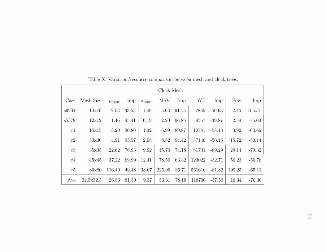
54
Table X. Variation/resource comparison between mesh and clock trees.
Clock Mesh
Case Mesh Size µskew Imp σskew MSV Imp WL Imp Pow Imp
s9234 10x10 2.03 93.55 1.00 5.03 91.75 7836 -50.63 2.46 -105.51
s5378 12x12 1.46 95.41 0.19 2.20 96.86 8557 -39.87 2.59 -75.00
r1 15x15 3.20 90.80 1.32 6.99 89.87 10781 -58.43 3.92 -60.66
r2 30x30 4.91 93.57 2.08 8.82 94.42 37146 -50.16 15.72 -50.14
r3 35x35 22.62 76.93 9.92 45.70 74.18 81731 -89.29 29.14 -79.32
r4 45x45 37.22 69.99 12.41 78.50 63.32 123022 -32.71 56.23 -56.76
r5 80x80 116.40 49.48 38.67 225.96 36.71 561616 -81.82 199.25 -65.11
Ave 32.5x32.5 26.83 81.39 9.37 53.31 78.16 118706 -57.56 18.34 -70.36

55
CHAPTER IV
METHODOLOGY AND ALGORITHMS FOR ROTARY CLOCKING
Rotary clocking has been shown to be a promising new clocking scheme that handles
both power and variation issues [10]. In this chapter, we discuss the issues involved
in using the current CAD flows for rotary clocks. We detail alternative flow and
algorithms.
A. Previous Work
(b)
180
270
90
0
135
225 45
(a)
315
Fig. 12. (a) A rotary clock ring. The numbers indicate relative clock signal phase. (b)
An array of 13 rotary clock rings. The small triangles points to the equal-phase
points for the 13 rings.
In order to solve the power and the variation problem more effectively, several
novel clocking technologies have been developed [10, 43, 44]. Among them, rotary
traveling wave clock [10] is a promising approach. The basic component of a rotary
clock is a pair of cross-connected differential transmission line circles, namely a rotary
clock ring (as shown in Figure 12(a)). A clock signal propagates along the ring without

56
termination so that the energy can be recirculated and the charging/discharging power
dissipation is greatly reduced. A recent study [45] shows that rotary clocks can
reduce power dissipation by 70% compared to conventional clock networks. The
measurement results from a test chip also showed that a low skew variation of 5.5ps
at 950MHz can be achieved [10]. Rotary clock can provide uniform clock signal
amplitude in contrast to the non-uniform amplitude in standing wave clock [43].
There is one technical hurdle that prevents wide applications of the rotary clock:
the clock signal has different phases at different locations on the rotary clock ring.
If zero skew design is insisted, the usage of rotary clocks would be very restrictive.
Hence, non-zero intentional skew design is a better approach to fully utilize the ro-
tary clock. Unlike the intentional skew design in the conventional clocking technology
where no restrictions are imposed on the flip-flop locations, the skew at each flip-flop
has to be matched with a specific location at the rotary clock ring. This requirement
forms a difficult chicken-and-egg problem: the flip-flop placement depends on skew
optimization while it is well known that skew optimization depends on flip-flop loca-
tions. This is quite different from traditional intentional skew designs [46] where the
placement does not depend on skew optimization.
The goal of this work is to break this technical hurdle so that rotary clocks can
be easily deployed in practice to alleviate the power and variation issues. We make
the following contributions in this work.
• A relaxation technique based on flexible tapping is suggested to break the loop
in the chicken-and-egg problem.
• An integrated placement and skew optimization methodology is proposed. This
methodology has the advantage that it fits well with the current CAD flow and
the placers can be used without any change.
• A min-cost network flow algorithm is found to assign flip-flops to the rotary clock

57
rings so that the movement of flip-flops has the least disturbance to traditional
placement.
• A pseudo net technique is introduced to guide flip-flops toward their preferred
locations without intrusive disturbance to traditional placement.
• A cost driven skew optimization formulation is developed to reduce the connec-
tion cost between flip-flops and their corresponding rotary clock rings.
• We develop an Integer Linear Programming (ILP) formulation to minimize the
maximum capacitance loaded at any rotary ring. Since the operating frequency
is inversely proportional to the load capacitance, this formulation could be used
in delay critical designs. We also detail a fast and effective heuristic used to
solve the formulation.
B. Rotary Traveling Wave Clock and Traditional Design Flow
In this section, we discuss the basics of rotary clocking, its advantages, whether a
rotary clock can fit into a traditional design flow and if not, what are the difficulties.
The basic component of a rotary clock is a pair of cross-connected transmission line
circles as shown in Figure 12(a). In the rotary clock ring, an oscillation can start
spontaneously upon any noise event [10]. When the oscillation is established, the
square wave signal can travel along the ring without termination. An arbitrary point
on the ring can be designated as the reference point with clock signal delay t = 0 and
clock phase φ = 0. Starting from this reference point, the clock signal travels along
the ring and reaches back to the reference point with delay equal to clock period
T and phase φ = 360. The numbers in Figure 12(a) indicate clock signal phases.
Clock signal delay t and clock signal phase φ can be converted to each other by
φ
360= t
T− ⌊ t
T⌋.

58
The energy loss due to the wire resistance is compensated by the anti-parallel
inverters as shown in Figure 12(a). In addition, these inverter pairs help to achieve
phase locking as the phases of the two circles at the same location are always opposite.
In order to maintain uniform capacitance distribution along the ring, dummy capaci-
tive load needs to be inserted at places where no flip-flops exist. In chip level designs,
multiple rotary clock rings can be connected together to form an array as shown in
Figure 12(b), where the dashed arrows indicate the signal propagation directions and
the small triangles indicate equal phase locations for all rings.
A rotary clock has the advantage of both low power dissipation and low skew
variation. It consumes less power as the energy is recirculated along the ring as
opposed to energy loss during the charging/discharging through transistors in con-
ventional clocking. In the rotary clock ring array (Figure 12(b)), the phase averaging
at the junction points can reduce skew variation remarkably.
In spite of the appealing advantages, the rotary clocking scheme is not compatible
with existing design flows. Consider the cross-coupled rings shown in Figure 12(b).
Since at each spot on a rotary clock ring, the clock signal has a distinct phase, a
zero clock skew design implies that only one spot on each ring can be utilized. In
Figure 12(b), there are 13 rings and there are only 13 useful spots for a zero clock skew
design. Obviously, such usage of rotary clock is very inefficient. In order to fully utilize
rotary clock, intentional skew design is a much better choice. Even with intentional
clock skews, rotary clocking poses an important problem. A typical intentional skew
design flow, which is employed in IBM high performance ASIC designs [46] proceeds
in the order of the following stages.
1. Placement. In placement [47, 48], cells are placed in a non-overlapping manner
so that an objective function, such as the total signal net wirelength, congestion,
critical path timing or a combination of them, is minimized.

59
2. Clock skew optimization. For intentional skew designs, clock signal delay target
to each flip-flop is found so as to minimize clock period or maximize timing
slack, subject to long path and short path constraints. Since the long path and
short path constraints depend heavily on cell and flip-flop locations, placement
information is essential in order to perform skew optimization. We will discuss
skew optimization in Section G.
3. Clock distribution network synthesis. In this stage, a clock distribution net-
work layout is generated to approximately deliver intentional skews [46], which
correspond to the clock delay targets obtained in skew optimization. Of course,
the clock distribution network layout depends on flip-flop locations.
The feasibility of this flow is based on its one-way dependency that each stage relies on
the result of the previous stages, but not vice versa. More specifically, the placement
(with the inclusion of flip-flops), does not depend on skew optimization or clock
distribution network synthesis. Likewise, skew optimization does not depend on clock
distribution network synthesis.
Rotary clock is usually designed independently. In placement, each flip-flop
needs to be placed at a rotary clock ring and the clock phase at its location has to
match the clock signal delay target for the flip-flop. This requirement causes a cyclic
dependency. The flip-flop placement depends on its clock signal delay target, which
is generated by skew optimization. But skew optimization is always dependent on
placement. This chicken-and-egg problem has to be solved to enable the application
of rotary clocking technique.
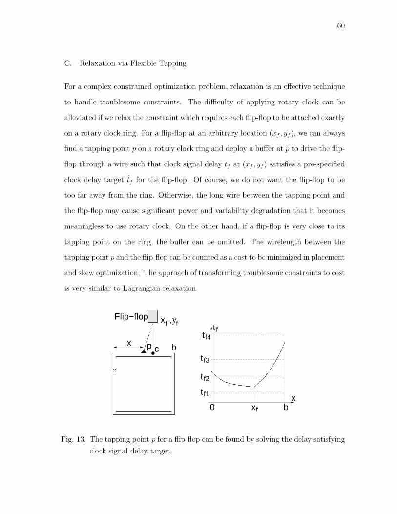
60
C. Relaxation via Flexible Tapping
For a complex constrained optimization problem, relaxation is an effective technique
to handle troublesome constraints. The difficulty of applying rotary clock can be
alleviated if we relax the constraint which requires each flip-flop to be attached exactly
on a rotary clock ring. For a flip-flop at an arbitrary location (xf , yf ), we can always
find a tapping point p on a rotary clock ring and deploy a buffer at p to drive the flip-
flop through a wire such that clock signal delay tf at (xf , yf ) satisfies a pre-specified
clock delay target tf for the flip-flop. Of course, we do not want the flip-flop to be
too far away from the ring. Otherwise, the long wire between the tapping point and
the flip-flop may cause significant power and variability degradation that it becomes
meaningless to use rotary clock. On the other hand, if a flip-flop is very close to its
tapping point on the ring, the buffer can be omitted. The wirelength between the
tapping point p and the flip-flop can be counted as a cost to be minimized in placement
and skew optimization. The approach of transforming troublesome constraints to cost
is very similar to Lagrangian relaxation.
,y
xbxf
x p
t
t f3
t f2
t f1
t f4
b
f
0
c
xf fFlip−flop
Fig. 13. The tapping point p for a flip-flop can be found by solving the delay satisfying
clock signal delay target.

61
Now we will show how to find the location of the tapping point so that the delay
target tf for the flip-flop at (xf , yf ) can be satisfied. We illustrate this procedure
through an example in Figure 13. A rotary clock ring is implemented in square shape
in layout and is composed by four inside segments and four outside segments, as
shown in Figure 13. Without loss of generality, we only consider the case when the
tapping point is on the top segment. Other cases can be derived in an almost identical
manner. We assume that the left end of the segment is set at coordinate (0, 0), the
location for the right end, the flip-flop and the tapping point are represented as (b, 0),
(xf , yf ) and (x, 0), respectively. If the delay of the clock signal at (0, 0) is t0, then
the delay at p can be expressed as t0 + ρx [10] with ρ being a positive constant. We
denote the distance between the tapping point and the flip-flop as l, assuming wire
resistance and capacitance per unit length are r and c, respectively. Let Cflip−flop
denote the input capacitance of the flip-flop. In order to satisfy the clock signal delay
target at the flip-flop, the clock signal delay tf has to satisfy:
tf (x) = t0 + ρx +1
2rcl2 + rlCflip−flop = tf (4.1)
Since l = |x− xf |+ yf , l is a function of x. The location of the tapping point can be
obtained by solving the above equation.
Figure 13 shows an example of curve tf (x) which is composed by two parabolas
joining at x = xf . The function tf (x) can be decomposed into a quadratic function
plus the term of |x−xf |. The quadratic function leads to a single parabola. However,
the term of |x − xf | consists of two pieces of linear parts with a non-differentiable
joint point at x = xf . Therefore, the overall shape of the tf (x) curve becomes two
pieces of parabolas joining at x = xf . Depending on the value of tf , there are four
cases for solving Equation (4.1).
• Case 1: tf is very small like tf1 in Figure 13. There is no direct solution for this

62
case. This case can be circumvented by reducing t0 by integer number of clock
period time T . Note that such reduction does not affect clock phase. This is
equivalent to lowering the curve tf (x) by multiple T and eventually results in
one of the following three cases. Obviously, the number of T for the reduction
needs to be minimized.
• Case 2: tf is moderately small like tf2 in Figure 13. There are two solutions in
the case and the solution with smaller wirelength is selected.
• Case 3: tf is at middle level like tf3 in Figure 13. There is a unique solution.
• Case 4: tf is large like tf4 in Figure 13. There is no direct solution for this case.
However, we can choose (b, 0) as the tapping point and intentionally introduce
wire detour between p and the flip-flop so that delay target tf is satisfied. This
is almost the same as the wire snaking in clock tree routing [18].
After the tapping points on each of the eight segments are calculated, the one leading
to the minimum wirelength is selected as the tapping point for the ring. The actual
wirelength for achieving the clock signal delay target is defined as the tapping cost.
Note that we could also use a buffer to drive the signal from point p. If needed,
equation (4.1) can be easily modified to take care of the buffer delay.
It may be noted that in a rotary ring, a phase and its complementary phase (two
phases are complementary to each other if they are 180 degrees apart, for example 90
and 270 are complementary phases) are available at points that are physically close
to each other. Let φ1 and φ2 denote the two complementary phases available at a
points p1 and p2 in the rotary ring. If two flip-flops F1 and F2 are both assigned to p1,
then one can connect F1 to point p1 (with phase φ1), F2 to point p2 (with phase φ2)
and assign opposite polarities to F1 and F2 (that is we can make one positive-edge
triggered and another one as negative edge triggered).

63
D. Proposed Methodology
The flexible tapping technique breaks the cyclic dependency between the placement
and skew optimization. It also facilitates a new methodology flow as shown in Fig-
ure 14, in which skew awareness for the placement is achieved indirectly through a
pseudo net technique. By doing so, the traditional placement methods can be used
without any change. This is an appealing feature because placement is a much more
complicated problem than skew optimization.
DoneY
N
Is cost satisfactory?
4. Cost driven skew optimization
5. Assign pseudo net and/or net weight
6. Incremental placement
1. Initial placement
2. Slack driven skew optimization
3. Assign flip−flops to rings
Fig. 14. Proposed methodology flow.
The first two stages are almost the same as the traditional flow. The initial
placement can be implemented with any existing placement method [47, 48] without
special considerations of flip-flop locations or their skews. In stage 2, skew optimiza-

64
tion [1] is performed based on the placement of stage 1 to maximize the timing slack.
The details of this part will be described in Section G.
In stage 3, each flip-flop is assigned to a ring of the rotary clock ring array. This
assignment only establishes an association between a particular flip-flop to a ring and
does not change the flip-flop location. When a flip-flop is assigned to a specific ring,
the corresponding tapping cost can be computed according to Section C. Depending
upon the design objective, we propose two different techniques for flip-flop assignment:
1. A network flow based assignment algorithm which aims at minimizing the total
tapping length subject to capacity constraints. This technique is detailed in
section E.
2. An Integer Linear Programming (ILP) based approach that aims at minimizing
the maximum capacitance loaded at any of the rotary rings. This technique
(detailed in section F) can be used in high speed designs.
After each flip-flop is assigned to a ring, another skew optimization can be performed
to reduce the tapping cost. This is somewhat different from traditional skew opti-
mization and will be discussed in details in Section G. After stage 4, the overall cost
is evaluated as a weighted sum of total tapping cost and traditional placement cost,
which is usually total signal wirelength. If the overall cost is sufficiently small, this
flow is completed. Otherwise, the flow proceeds to stage 5.
Since the initial placement is based on the traditional objectives such as signal
wirelength and ignores tapping cost, it is quite likely that the tapping cost is very
high when we enter stage 5 for the first time. In order to reduce tapping cost, we
insert a pseudo net between each flip-flop and its ring. The flip-flops can be pulled
toward their associated rings in the placement stage 6. Since stage 6 is an incremental
placement, it normally runs considerably faster than the initial placement. Of course,

65
the incremental placement is preferred to be a stable one [47], i.e., small changes on
the netlist should not cause dramatic change on the placement result.
E. Flip-flop Assignment to Minimize Tapping Cost
In stage 3 of the above flow, each flip-flop needs to be assigned to a ring in the rotary
clock ring array. It is required that the assignment minimizes the tapping cost defined
in Section C. We denote the tapping cost as ci,j, when a flip-flop i is assigned to ring
j. Each ring j has limited space and can accommodate no more than Uj flip-flops. We
introduce a decision variable xi,j: if flip-flop i is assigned to ring j, xi,j = 1, otherwise
xi,j = 0. The flip-flop assignment problem can then be formulated as the following
0-1 programming problem.
Minimize∑
i,j ci,jxi,j
Subject to∑
j xi,j = 1 ∀i∑
i xi,j ≤ Uj ∀j
xi,j ∈ 0, 1 ∀i, j
S
0/1
Ring k
Ring 1
Ring 2
0/U
c /1
c /1
0/U0/1
1,1
m,k
T
FF1
FFm
FF2
k
1
Fig. 15. Min-cost network flow model for flip-flop assignment. Each arc is associated
with cost/capacity.
This assignment problem can be solved using min-cost network flow model [49]

66
as shown in Figure 15. The vertices in the network include a column of flip-flop
vertices, a column of ring vertices, a source vertex and a target vertex. There is an
arc from a flip-flop vertex to a particular ring vertex only if the corresponding flip-flop
is considered to be a potential candidate of the ring. If a flip-flop and a ring are too
far away from each other, it is not necessary to insert an arc between them. Each arc
between a flip-flop vertex i and a ring vertex j has a cost of ci,j. The rest arcs have
zero cost. Each arc from a ring vertex j to the target vertex has a capacity of Uj.
The other arcs have a capacity of 1. It is well known that this min-cost network flow
problem can be solved optimally in polynomial time [49].
F. Flip-flop Assignment to Minimize Load Capacitance
In this section, we present an alternative formulation that can be used in place of the
one discussed in section (E). The frequency of operation of the rotary clock is given
by [50]:
fosc =1
2√
LtotalCtotal
(4.2)
Ctotal consists of two components - the ring capacitance and the capacitance of the
load that the ring drives. The latter shall hence forth be referred to as load capac-
itance. Since the ring capacitance for a given ring dimension is a constant, we can
minimize Ctotal by minimizing the load capacitance. If the design objective is to run
the maximum possible frequency, then the load capacitance at the rings is a more rel-
evant optimization objective. The network flow formulation discussed in section (E)
attempts to distribute the flip-flops uniformly across the rotary rings while optimiz-
ing the tapping length. While this is ideal if the design objective is to minimize the
tapping length, it is not a direct measure of the load capacitance.
We present an alternative formulation which takes into account the load capaci-

67
tance at the rotary rings. Let Cijp denote the load capacitance of a flip-flop i when it
is assigned to a ring j. This capacitance includes both the interconnect capacitance
as well as the flip-flop input capacitance (or buffer capacitance). Let xij denote the
indicator variable that is set to one if flip-flop i is assigned to ring j and zero other-
wise. Then the formulation to minimize the maximum load capacitance can be stated
as follows:
min max∑
Cijp xij (4.3)
∑
∀j
xij = 1∀i
xij ∈ 0, 1
The following key observations can be made about formulation (4.3):
• The cost (Cijp ) is a direct measure of the load capacitance in contrast to the
cost used in formulation (4.2)
• The formulation is an integer programming (ILP) problem. ILP in general is
NP-hard and hence there is a need to employ fast and effective heuristics.
1. Solution by LP-relaxation
LP-relaxation has been used to solve a certain class of combinatorial optimization
problems like the set cover [51]. The basic steps involved in LP-relaxation are as
follows:
1. Relax the integer constraints (usually 0-1 constraints on decision variables) to
continuous constraints. For example an integer constraint xij ∈ 0, 1 would be
replaced by 0 ≤ xij ≤ 1.
2. Solve the resulting LP. For a minimization problem, the optimal solution to the

68
LP gives a lower bound on the optimal solution to the ILP. This is due to the
fact that any feasible solution to the ILP is also a feasible solution to the LP.
3. Now round the LP solution to the get an integer solution.
The key to any LP-relaxation procedure is the rounding process. The rounding pro-
cess should be such that (a) Feasibility of the ILP is maintained and (b) The deviation
of the objective function is minimized. With the above two restrictions in mind, we
employ a rounding procedure which shall henceforth be referred to as greedy round-
ing.
Let I denote the set of flip-flops, J the set of rotary rings, X lp = xlpij the
solution obtained from the LP-relaxation and X ilp = xilpij the ILP solution obtained
on LP-rounding. For feasibility, we need to make sure that each flip-flop is assigned
to exactly one ring. This is done by ensuring upon rounding xilpij is set to exactly one
j ∈ J .
The greedy rounding procedure is described in Figure (16). If the LP solution
also happens to be integral, we retain it. If not each flip-flop i is assigned to the ring
j whose corresponding assignment variable xlpij is maximum. Hence our procedure is
referred to as greedy rounding. The complexity of the rounding procedure is linear in
the number of flip-flops and the number of rings. Since the number of rings is much
smaller than the number of flip-flops and the solution to LP generally runs in linear
time (in practice), the overall procedure of greedy rounding is linear in the problem
size.
Let OPT (LP ) denote the optimum solution of the LP-relaxation and SOLN(ILP )
denote the solution of obtained after solving the ILP (by any procedure). Then we

69
define integrality gap IG as:
IG =SOLN(ILP )
OPT (LP )(4.4)
The following observations can be made about IG:
1. IG ≥ 1, since the LP solution is always lower than the ILP solution.
2. ILP in general is NP-complete. But, whether the ILP described in Equa-
tion (4.3) can be solved optimally in polynomial time remains open. Since
we currently do not know the optimal solution, IG acts as a good base case for
comparison.
3. The value of IG should not be interpreted in an absolute sense. For example,
IG = 1.40 does NOT mean that the solution of the heuristic is 40% away from
optimal value.
In order to compare the efficacy of the proposed heuristic, we ran the same
formulation using a public domain ILP-solver [52]. Table (XI) presents the comparison
between greedy rounding and ILP-solver. The comparisons are made in terms of
both run-time and quality of solution (measured by the Integrality Gap). While
greedy rounding produced a solution within few seconds, the ILP-solver took several
hours. We bounded the simulation time for the ILP-solver to 10 hours and report
the best solution that it produced within this time. For 3 of the test cases, the ILP-
solver did not produce a feasible solution. For the remaining 2 the greedy rounding
outperformed ILP-solver by a significant margin. This is not unexpected since the
ILP solver is generic in nature whereas our rounding procedure exploits the problem
structure.
It was observed that the ILP formulation reduces the maximum capacitance
significantly. But this reduction comes at the expense of increased signal and clock

70
Table XI. Integrality gap of greedy rounding and ILP-solver.
Circuit Greedy Rounding ILP-Solver
IG CPU(s) IG CPU
s9234 1.32 0.25 1.83 > 10hrss5378 1.57 0.31 22.05 > 10hrs
s15850 1.32 2.0 – > 10hrss38417 1.23 6.10 – > 10hrss35932 1.63 13.10 – > 10hrs
wire length. The details are discussed in section (H).
Procedure: Greedy Rounding
Input: X lp = xlpij: Solution for the relaxed LP
I - set of flip-flops, J - set of rings
Output: xilpij : Solution to the ILP
1. For each i ∈ I do
1.1 If xlpij1
= 1 for some j1 ∈ J ,
xilpij1
= 1 and xilpij = 0 ∀j 6= j1
1.2 Else
Find jmax ∈ J such that
xlpijmax
≥ xlpij∀j ∈ J
xilpijmax
= 1 and xilpij = 0 ∀j 6= j1
2. Return X ilp = xilpij
Fig. 16. Greedy rounding algorithm.
G. Skew Optimization
Skew optimization is an important part of the proposed flow. The skew optimization
in stage 2 is the same as the max-slack version of the traditional method [1] and we
summarize it here for completeness. If two flip-flops i and j are said to be sequentially
71
adjacent if they have only combinational logic between them. Sequential adjacency is
denoted by i 7−→ j. Let Dijmax (Dij
min) denote the maximum (minimum) combinational
logic delay between i and j. Let ti denote the clock signal arrival time at i, tsetup (
thold) the setup (hold) time and T the clock period. Then the max-slack version of
skew optimization can be formulated as [1]:
Maximize M (4.5)
Subject to ti − tj + M ≤ T −Dijmax − tsetup i 7−→ j (4.6)
ti − tj ≥M + thold −Dijmin i 7−→ j (4.7)
where M is the slack. Inequalities (4.6) and (4.7) are referred to as the long path
constraint and short path constraints, respectively. It has been shown that this
problem can be solved using linear programming [1] or graph based algorithms [19, 23].
We propose a cost driven method so that skew optimization can be leveraged to
assist placement on reducing the total tapping cost. The computation of the tapping
cost (Section C) is based on a known clock signal delay target while the delay target
is a decision variable in skew optimization. Therefore, we try to minimize the tapping
cost indirectly by finding clock signal delay targets such that the tapping point can
be moved to the flip-flop as close as possible. For example, in Figure 13, if the
delay target of the flip-flop can result in tapping point at c, then the tapping cost is
minimized. In other words, if the actual delay to a flip-flop i is ti through tapping
point at c, we try to make the delay target ti to be as close to ti as possible.
For flip-flop i, we first find the closest point c on its ring and the distance between
i and c, which is the shortest distance between i and the ring, is denoted as li. The
delay ti at i through tapping point at c depends on the reference clock signal delay on
the rotary clock rings. We can arbitrarily choose a set of equal phase points for all the
72
rotary clock rings as reference points like the small triangular spots in Figure 12(b).
Let the clock signal delay at the reference points be tref . If the delay from the
reference point to c is tref,c, then the clock signal delay at c is tc = tref + tref,c. The
delay from c to i is tc,i = 12rcl2i + rliCflip−flop which is very similar to Equation (4.1).
Hence, the clock signal delay at i is ti = tc + tc,i, If the difference |ti− ti| is minimized,
there is a good chance that the tapping point is the closest to c and the flip-flop.
When a flip-flop i is far from its ring, i.e., tc,i is large, it is especially desired that the
tapping point is closest to c. Therefore, |ti − ti|+ tc,i is minimized in the cost driven
skew optimization.
Minimize ∆
Subject to ti − tj + M ≤ T −Dijmax − tsetup i 7−→ j
ti − tj ≥M + thold −Dijmin i 7−→ j
tref + tref,c + 2tc,i − ti ≤ ∆ ∀i
ti − tref − tref,c ≤ ∆ ∀i
where ∆ is the maximum difference and M is a pre-specified slack. The constraint
from the two inequalities in this formulation is equivalent to |ti − ti| + tc,i ≤ ∆.
Obviously, this problem can be solved through linear programming [1].
Alternatively, the skew optimization problem can be formulated to minimize a
weighted sum of the differences as follows.
Minimize∑
∀i wiδi
Subject to ti − tj + M ≤ T −Dijmax − tsetup i 7−→ j
ti − tj ≥M + thold −Dijmin i 7−→ j
ti − ti ≤ δi ∀i

73
ti − ti ≤ δi ∀i
where δi is the difference for flip-flop i and wi is its weighting factor. A natural choice
of the weighting factors is to let wi = li, as we wish to focus our effort on those flip-
flops far away from their rings. Again, this problem can be solved directly through
linear programming [1].
H. Experimental Results
The proposed methodology and algorithms are tested on the ISCAS89 benchmark
suite. The benchmark characteristics are summarized in Table (XII). The first four
columns indicate the circuit name, number of standard cells, number of flip-flops
and the number of nets respectively. In the fifth column of Table (XII), we report
average source-sink path length in conventional clock trees [17, 20] for reference. The
number of rotary rings for each test case is indicated in the final column. The rotary
clock ring arrays are generated as in [10]. The operating frequency was set at 1GHz.
The circuits are synthesized using SIS [41]. The main algorithms are implemented
in C++. The initial placement as well as the incremental placement are obtained
from an academic placement tool mPL [48, 42]. Soplex was used to solve the LP-
relaxation problem [53]. All experiments are performed on a Pentium 4 workstation
running Linux operating system with 1 GB RAM. The interconnect parameters are
obtained from bptm [40]. The skew permissible ranges can be computed using any
static timing analysis tool as detailed in [1]. We used the Elmore delay model [16] in
our static timing analyzer. However, our techniques are generic and can be extended
to more accurate timing analysis tool without any changes in the underlying skew
optimization algorithms or the overall flow.
To the best of our knowledge, there is no published work on placement and skew

74
Table XII. Testcases. PL is the average source-sink path length in conventional clock
trees [17, 20].
Circuit #Cells #Flip-flops #Nets PL(µm) # Rings
s9234 1510 135 1471 2471 16
s5378 1112 164 1063 2718 25
s15850 3549 566 3462 5175 36
s38417 11651 1463 11545 8261 49
s35932 17005 1728 16685 8290 49
optimization for rotary clocking. There are three issues which we care about:
1. Each flip-flop needs to be close to the ring it associated with so that the off-ring
variation effect is negligible
2. Moving flip-flops toward their associated rings should not degrade signal wire-
length significantly and the total wirelength including tapping wirelength needs
to be minimized.
3. If the design objective is speed, then the maximum load capacitance at any of
the rotary ring should be minimized.
Table (XIII) gives the results for the base case. These results (base case) are
obtained by running the flip-flop assignment algorithm using network flow at stage 3
of our overall flow (indicated in Figure (14)). In all the tables shown, AFD denotes
the Average Flip-flop Distance and WL the wire length. All wire lengths are reported
in µm, capacitances are reported in pF and power in mW . Table (XIII) presents the
AFD, tapping wirelength, signal wirelength, total wirelength, power dissipation in
the clock net, power dissipation in the signal net and total power dissipation for the
75
base case. It can be seen that the average flip-flop distance is significantly smaller
than the average source-sink path length in conventional clock trees [17, 20] (as shown
in the rightmost column of Table (XII)). The power dissipation is obtained by the
technique(s) detailed below. The power dissipation in the clock net includes the
dynamic power dissipated in the tapping wires from the rotary ring as well as the
power dissipated in the flip-flops. The power dissipated in the signal length includes
the power dissipated in the interconnect, logic gates as well the the buffers. The
power dissipation is measured using the following formula.
Pdynamic =1
2αV 2
ddfclkCload (4.8)
In the above equation, α denotes the switching activity, fclk the clock frequency, and
Cload the total capacitive load and Vdd the supply voltage. For the clock net, α is
set to 1. Estimating α for signal net is a hard problem and setting it to 0.15 usually
gives a reasonable approximation [5]. For clock nets, we know the actual interconnect
capacitance and the flip-flop capacitance accurately and hence estimating the power
is straightforward. The capacitance in the signal net consists of three components:
(a) the interconnect capacitance (b) the input capacitance of logic gates and (c) the
input capacitance of the buffers used in the signal net. The first two capacitances are
easy to estimate since we have a placed/mapped design. To estimate the number of
buffers in the signal net, we use the technique detailed in [54]. The above technique
estimates the buffer delay (while estimating the number of buffers inserted) at an
early stage (floorplan) with a reasonable accuracy. Thus we estimate the dynamic
power dissipated at the clock and signal net and sum them up to get the total power.
The total leakage power in a circuit can be approximated to [5]:
Pleakage = VddIoff (S + NF SF ) (4.9)

76
In the above equation Ioff denotes the unit leakage current, NF the total number of
flip-flops, S the total inverter size and SF the gate size of one flip-flop. Since our
methodology does not change the gate sizes in the mapped design, the leakage power
remains largely unaffected and so we concentrate on the dynamic power dissipation
alone.
Table (XIV) gives the results on running stages 4-6 in our overall flow along with
the improvements from stage 3 (as reported in Table (XIII)). The data shows that
the iterations of stage 4-6 can reduce tapping wirelength by 37%-52% with only 1.3%-
4.06% penalty on signal wirelength increase. In fact, the total wirelength is reduced
by 2.6%-6.0%. After the iterations of stage 4-6, the average distance has reduced to
the range of 100 − 200µm, which is significantly smaller than the stub length limit
indicated in [10]. The CPU time is reported at the rightmost column of Table (XIV).
As one can see, most of run time is dominated by the placer. Our method converges
within five iterations for all these circuits.
Table (XV) presents the results for maximum load capacitance for the network
flow and ILP formulations. We compare the AFD, maximum cap and total signal
wirelength of the two techniques. We observe that ILP based formulation reduces
the maximum load capacitance by 25.7%-48.33%. However it increases the AFD (by
11.32%-30.82%) and total wire length (by 0.15% -7.09%). This is expected since the
formulations target different objective. Hence the designer can choose between the
two formulations depending upon the optimization objective. The run time for the
ILP is low as explained in section (F) (Table (XI)) and repeated here for the sake of
completeness.
Table (XVI) gives the power dissipation results (in mW ) for network flow and
the ILP formulations. The results (clock, signal and total power) are then compared
with those obtained for the base case (shown in Table (XIII)) and the percentage

77
Table XIII. Experimental results for the base case, wirelength in µm, power in mW .
AFD Tap. WL Signal WL Tot. WL Clock Power Signal Power Tot. Power CPU(s)
s9234 285.6 38550 244485 283035 5.06 6.72 11.78 70
s5378 194.1 31839 260931 292770 4.67 6.84 11.51 158.1
s15850 266.6 150907 643336 794243 20.16 18.07 38.23 399
s38417 383.5 559586 1634920 2194506 68.8 48.35 117.15 410
s35932 340.8 588823 1735820 2324643 74.17 57.88 132.05 423

78
Table XIV. Experimental results for network flow based optimization, wirelength in µm.
AFD Tap. WL Signal WL Tot. WL CPU(s)
Circuit Final Imp Final Imp Final Imp Stg 2-5 mPL
s9234 136.3 18395 52.28% 247797 -1.35% 266192 5.95% 59 283
s5378 124.51 20419 35.87% 263878 -1.13% 284297 2.89% 25 439
s15850 168 95136 36.96% 664534 -3.3% 759670 4.35% 186 995
s38417 222.9 326136 41.72% 1701352 -4.0% 202744 7.61% 192 930
s35932 223.12 385555 34.52% 1799431 -3.67% 2184986 6.0% 195 1153
79
Table XV. Comparison of network flow and ILP formulations, cap in pF .
Network Flow ILP Formation
Circuit Cap AFD Imp Cap Imp Tot. WL Imp CPU(s)
s9234 0.49 178.25 -30.82% 0.33 32.65% 273633 -2.8% 0.25
s5378 0.39 138.6 -11.32% 0.29 25.64% 284297 -0.15% 0.31
s15850 1.23 205.8 -22.5% 0.70 43.1% 759670 -1.94% 2.0
s38417 2.52 274.2 -23.0% 1.34 46.83% 2027488 -6.59% 6.10
s35932 1.8 276.54 23.9% 0.93 48.33% 1927039 -7.09% 13.1
80
Table XVI. Power dissipation results (mW ) for network flow and ILP formulations.
Network Flow Formulation ILP Formation
Circuit Clock Imp Signal Imp Total Imp Clock Imp Signal Imp Total Imp
s9234 3.08 39.13% 6.78 -0.89% 9.86 16.3% 3.63 28.26% 6.81 -1.34% 10.44 11.38%
s5378 3.55 23.98% 6.89 -0.73% 10.44 9.3% 3.79 18.84% 6.84 0% 10.63 7.65%
s15850 14.67 27.23% 18.45 -2.1% 33.12 13.37% 16.77 16.82% 18.06 0.06% 34.83 8.89%
s38417 45.82 33.4% 49.56 -2.5% 95.38 18.58% 53.21 22.66% 48.19 0.33% 101.4 13.44%
s35932 54.15 26.99% 59.05 -2.02% 113.2 14.27% 63.24 14.74% 52.64 9.05% 115.88 12.25%
Ave 29.55 30.15% 28.15 -1.65% 52.4 14.36% 28.13 20.26% 26.51 1.62% 54.64 10.72%

81
Table XVII. Wirelength capacitance product comparison.
Circuit Network Flow, WCP ILP Formation, WCP Imp
s9234 130434 90298.9 30.77%
s5378 110717.6 82446.1 25.53%
s15850 934394.1 542083.5 41.99%
s38417 5109269.8 2895290.9 43.32%
s35932 3238975.8 1792146.3 44.67%
improvement is also reported. The network flow algorithm gives an average power
improvement of 14.36% whereas the corresponding improvement for the ILP formu-
lation is 10.72%. This is expected since the network flow algorithm tries to minimize
the total tapping length which in-turn minimizes the clock net length and the power
dissipation. It may be noted that the trend in power dissipation follows that of
wirelength reduction for both clock and signal nets (as expected).
It is often difficult to compare two techniques that have different optimization
objectives. In such cases, it is better to come up with one objective that can be
used for comparison. A classic example of such a case is the Power-Delay-Product
(PDP). In circuit optimization (especially gate-sizing), one could trade-off power for
delay improvement and vice-versa. Hence PDP is used a metric to compare different
techniques. In our methodology we trade-off wirelength and maximum load capac-
itance and hence we introduce the metric Wirelength-Capacitance-Product (WCP).
This has obvious parallels with the PDP since wire length is directly related to power
dissipation and maximum load capacitance is related to delay. Table (XVII) presents
the results for both the techniques in terms of WCP. WCP is reported in µm pF . It
may be observed that the ILP formulation results in much better WCP.

82
CHAPTER V
COMBINATORIAL ALGORITHMS FOR FAST CLOCK MESH OPTIMIZATION
We present fast and efficient combinatorial algorithms for clock mesh optimization.
Our contributions in this work are two-fold. We first present a set-cover based formu-
lation that performs simultaneous mesh buffer placement and sizing. We also present
mesh reduction algorithms that trade off skew tolerance for low power dissipation.
This algorithm gives a framework for the designer to choose the desired trade off
point (between circuit delay and power dissipation).
A. Preliminaries
We shall introduce certain notations and conventions which will be followed through-
out this chapter.
• m × n denotes the dimension of the clock mesh. I denotes the set of nodes in
the mesh.
• Clock buffers of B sizes b1, b2, . . . bk in non-decreasing order. Buffer bi can
drive a load of capacitance at most ci.
• Buffer Mapping Function BM : i→ j maps each node location i ∈ I to j ∈ B.
BM(i) = φ implies that the location i has no buffer in it.
• S = s1, s2 . . . sc denotes the set of clock sinks. Without loss of generality, we
assume that each sink si is connected to node i ∈ I (in reality, the clock sinks
will be connected to the closest point in the mesh which need not be in the
intersection of the horizontal and vertical grid lines). The node i in the mesh is
referred to as the connection node of sink si. dij denotes the minimum distance

83
between node i and j in the mesh.
• Tclock, thold and tsetup denote the clock period, hold time and set up time respec-
tively.
• The maximum permissible delay of logic network between any two registers
(i, j) is given by [1]:
P ijdelay = Tclock − tsetup − skewij (5.1)
• Pdelay = min∀(i,j)Pijdelay denotes the maximum permissible delay of the entire
circuit.
B. Previous Work
Clock Sinks
Mesh Buffers
Fig. 17. Mesh driven by a top level tree.
One of the most widely used non-tree based CDN is clock mesh. Figure (17)
shows a typical clock mesh [55, 50, 25]. The mesh consists of a rectangular grid

84
driven by a top level tree. The buffers at the leaf of the top level tree shall henceforth
be referred to as mesh buffers. The clock sinks or subnetworks are connected to
the closest point in the mesh. Since there are several paths between the source and
the clock sinks, there is a high level of redundancy and this redundancy translates to
high tolerance to variations in clock skew. Mesh architecture is used mainly in high
performance systems. In fact, it has been used in commercial microprocessors such
as IBM G5 [11], Power4 [12] and SUN Sparc V9 [13]. In all the above processors,
a very low clock skew has been reported which proves the effectiveness of the clock
mesh in mitigating skew variability.
The skew tolerance in mesh based architecture does not come for free. Clock
mesh consumes significantly higher wire area compared to tree based distributions.
In fact, a hybrid mesh architecture could consume up to 168% higher area compared to
tree [56]. Higher wire area leads that a higher load capacitance for the clock buffers
which in turn implies a higher power dissipation. There is an increasing demand
to deliver devices with higher battery life - even at the expense of lower operating
frequency. It is possible that future designs may trade off frequency for lower power
dissipation.
The maximum permissible delay of logic network between any two registers (i, j)
is given by Equation (5.1). The maximum permissible delay is a more direct metric
to evaluate circuit characteristic than clock skew. Skew becomes important when
it affects circuit delay (for example, in non-zero skew design, skew could be made
intentionally to deviate from zero to meet the delay specifications). Typically, in the
zero skew design skewij is designed to be zero. However, this may increase due to
variations subsequently reducing the maximum speed at which the circuit can func-
tion. Higher skew would bring down the maximum permissible delay Pdelay. Hence a
mesh architecture is suited well for high performance systems since it mitigates the

85
variations in clock skew even though the resource consumption is high (wire length,
power etc.). With power occupying an increasingly important role in chip design, it
is necessary to find the most desirable skew-power trade off. At the very least, the
designer should be given the flexibility to do so. For CDN design, this could imply a
higher skew for lower power dissipation. Since a significant portion of the total power
consumption comes from the clock network (up to 40% of the total power dissi-
pated in high performance systems [57]) and clock mesh consumes a high area/power
overhead, there is a need to address more efficient ways of designing/optimizing the
clock mesh. Even though there has been previous works on in mesh architecture, the
following issues remain largely unaddressed:
• What are the ideal locations for the mesh buffers to drive the clock mesh? Is it
ok to distribute the mesh buffers uniformly across the mesh?
• Can the mesh buffers be sized differently? If yes, then does it work better than
sizing uniformly?
• A mesh has a high level of redundancy. Can some amount of redundancy be
sacrificed to reduce the wire length? If yes, then how much is the trade-off?
Can we quantify the skew vs power trade-off?
In this work, we address all the above mentioned issues. Our contributions include:
• We propose a set-cover based algorithm for finding the mesh buffer locations
and their sizes. Our algorithm works fast on a discrete library of buffer sizes.
We show that such a buffer placement and sizing yields better results compared
to uniform sizing.
• We formulate the mesh reduction problem by using survivable network the-
ory. We present heuristics for solving the formulation efficiently. Experimental

86
results indicate up to 29% reduction in wire length, 28% reduction in
power with less than 3.3% increase in delay penalty.
• Our techniques allow the designer to trade-off between skew and power dissipa-
tion. In fact, the formulation presented is flexible enough to allow a high range
of trade-off (that is either a high skew- low power design or a low skew - high
power design or anywhere in between).
• Our algorithms run very fast. It can process test cases with over a thousand
sinks within a few seconds. Such a high speed helps the designer to run the same
algorithm several times with different parameter values that produce different
solutions in the power delay curve.
C. Problem Statement
Simultaneous Mesh Buffer Placement and Sizing
Find the function BM or for each candidate buffer location (there are m · n such
locations), find (a) If a buffer is required and (b) The size of buffer needed such that
the following constraints are satisfied: (i) Each node in the mesh is allocated to at
least one buffer, (ii) Each buffer drives less than the maximum load it can drive, and
(iii) The total sum of the buffer sizes is minimized.
Mesh Reduction
Remove edges from the mesh such that (i) Each sink si has at least k node locations
such that for each such node location j, dij ≤ Lmax, BM(j) 6= φ and there exists
at least l edge disjoint paths between j and i, (ii) The number of edges removed is
maximized. k, Lmax and l are user defined constants.
The mesh reduction problem attempts to remove edges such that there exists at least
certain number of buffers that connect each clock sink with short paths. The user

87
defined parameters control impact the solution in the following manner: Setting k
and l high would mean more redundancy and hence more tolerance to variations but
less number of edges removed or more power dissipation. By varying the parameters k
and l, the designer has the flexibility to trade variation tolerance to power dissipation.
The restriction Lmax helps in restricting the delay between the mesh buffers and the
clock sinks. This in turn, helps in keeping the skew low.
The buffers are sized with the assumption that they are driving a complete mesh.
After mesh reduction, the buffers could be driving a load that is significantly lesser
than that of a complete mesh. Hence, as a post-processing step, we compute the new
load and down-size the buffers accordingly. This procedure (as indicated in Figure 18)
will be detailed in this chapter.
D. Simultaneous Mesh Buffer Placement and Sizing via Set Cover
1. Algorithm Description
The Set Cover problem can be stated as follows: Given a set universe U and a col-
lection S of subsets of U , find a minimum size subset C ⊂ S such that C covers U . The
above definition can be modified to weighted set cover problem by assigning weights
of each set in S. In this section, we shall show that the mesh buffer placement/sizing
problem can be formulated as an instance of the set cover problem.
For each node in the mesh, define a Covering Region as follows. Covering
Region of the node for a particular buffer is defined as the set of nodes around
the node in the 2-dimensional mesh such that the total capacitance of the nodes
included in the covering region (including the mesh capacitance as well as the nodes
that the mesh drives) is less than the maximum capacitance that the buffer can drive.
Figure (19) depicts the covering region of a buffer placed at a point in a 2-dimensional

88
Complete Meshk, l, Lmax values
Simultaneous buffer
Placement/Sizing via set cover
Mesh reduction via
Steiner Network
to resize buffersPost−process reduced mesh
Fig. 18. Overall flow for mesh buffer sizing and reduction.

89
mesh grid. The dashed lines indicate the regions of the mesh that can be driven by
the buffer without violating the maximum load constraint of the buffer. If any more
edges in the mesh are added, then the capacitance of the region will be greater than
the maximum load that the buffer can drive. Let CRji denote the covering region of
node i ∈ I while driven by buffer j ∈ B. That is CRji ∈ I for each i ∈ I and j ∈ B.
Let SCR denote the super set of covering regions. We can draw the parallels between
the above defined variables and the instance of set cover defined earlier:
• The set of I of node locations can be considered as the universe U .
• The covering regions CRji form the collection of subsets S.
• If the buffer size bj denotes the weight of a subset CRji , then the objective is to
“pick” minimum weighted sum of subsets such that each node has at least one
subset covering it.
In other words, the mesh buffering problem is identical to the set cover problem with
I ⇔ U and SCR ⇔ C. If CRji is picked, then node i ∈ I is driven by buffer
j ∈ B. For example, consider a 2x2 mesh whose nodes are numbered 0, 1, 2, 3. Let
the number of buffer types be 2 namely (a, b). The number of subsets would then
be 8. Let the subsets be numbered (a0, a1, a2, a3, b0, b1, b2, b3). If the solution picks
subset a0, then node “0” of the mesh will be driven by buffer type “a”.
To motivate the solution approach, we shall now state the same problem in
mathematical terms using indicator variables. Let xji denote the indicator variable
that is set to 1 if CRji is picked in the solution. Then the problem can be stated as:
minimize∑
j∈B
∑
i∈I
bjxji (5.2)
∪(i,j):xji=1CRj
i ⊇ I

90
Clock Sink
Clock Sink
Dashed lines indicate covering region of the buffer shown
Mesh Buffer
Fig. 19. Example of covering region.
Note that irrespective of the approach towards solving the set cover problem, it is
possible that the algorithm may return two buffers for the same location, which is
not a feasible solution. However such a situation can be easily avoided by using the
observation and lemma stated below.
Observation 1: For any node i ∈ S, CRji ⊇ CRl
i if bj > bl. The observation comes
from the fact that a bigger buffer size can drive a bigger load.
Lemma 1: In any optimal solution Φ, for any node i, there can be at most one buffer
j such that xji = 1.
Proof: Direct consequence of Observation 1. If there exists two buffers j and l such
that xji = 1 and xl
i = 1 and bj ≥ bl, then CRli can be removed from Φ without loss of
feasibility. This implies that Φ is not optimal and hence a contradiction.
Corollary 1: In any solution Φ, for any node i, if there are more than one buffer
driving a node, one can pick the biggest buffer without losing feasibility.
At the end of algorithm, the solution is pruned using Corollary 1.
Although there are several ways to implement the set cover algorithm, we shall

91
implement it using the greedy algorithm. The greedy algorithm can be stated as
follows: Pick the set that covers the most nodes and then throw away the nodes that
are covered. Repeat this process until all nodes are covered. The greedy algorithm is
simple, yet has a proven approximation guarantee. If OPT is the value of the optimal
solution and |U| is the size of the universe U , then it can be shown that the greedy
algorithm produces a solution of size at most OPT (ln( |U|OPT
) + 1) [51]. This essen-
tially proves that greedy algorithm has an approximation guarantee of O(ln(|U|)).
Inapproximability results show that this is the best approximation guarantee that
any algorithm can produce for the set cover problem [58]. The algorithm is detailed
in Figure (20). Notice that we have modified the algorithm slightly to take care of
set weights (in this case the buffer sizes). As it will be detailed in the experimental
section, the set cover implementation runs very fast in practice (within few seconds
a test case with more than 1700 sinks).
2. Complexity Analysis and Near-Continuous Sizing
In this section, we present the complexity analysis and show how our algorithm can
be extended to continuous sizing (in practice). Let α denotes the minimum size of a
subset. In other words, α denotes the minimum number of nodes in the mesh covered
by the minimum buffer size in the library. Let N denotes the number of nodes in
the mesh and β the size of the buffer library. Since each iteration of the algorithm
(in Figure (20)) covers at least α nodes, it is easy to see that the complexity of
the algorithm is O(Nβ
α). Essentially, the algorithm is linear with the mesh size and
number of buffer types. Figure (2) shows the plot of CPU time verses the number of
buffer types for the test case s35932. The figure illustrates the following aspects of
our buffer placement/sizing algorithm:

92
1. The run time increases linearly with number of buffer types.
2. We ran the experiment with 41 buffer types. The minimum and maximum
buffer sizes were set to 20x and 60x times that of a minimum size inverter. In
other words, we had a buffer size granularity equal to the size of a minimum
inverter. Our set up is equivalent to near continuous sizing. Even in such a
scenario, the run time of our algorithm (as indicated in Figure (2)) was about
half a minute. Hence we can conclude that our algorithm is expendable for
large library sizes as well as continuous sizing - if necessary.
Greedy set cover for mesh buffer placement/sizing.
Input : SCR = ∪ CRji for each i ∈ I and j ∈ B
Output : M = set of covering regions that are picked
1. M ← φ
2. While M does not cover I do
2.1 For each unpicked covering region CRji
define Ceff = bj
|CRji−M |
2.2 Pick set C with least Ceff .
2.3 M ←M ∪ C
3. For each node i ∈ I, if there exists j ∈ B and l ∈ B
both CRji and CRl
i are picked and bj > bl
drop CRli from the solution.
Fig. 20. Greedy set cover for mesh buffer placement/sizing.

93
5
10
15
20
25
30
35
5 10 15 20 25 30 35 40 45
CP
U ti
me
(sec
)
# Buffer Types
CPU time Vs # Buffer Types
Fig. 21. CPU time vs # buffer types for s35932.
E. Mesh Reduction and Post-Processing
1. Mesh Reduction
Once we locate the position of the mesh buffers and their sizes (from the buffer
library), the next task is to reduce the size of the mesh. This is done by removing
edges such that a certain level of redundancy is still maintained. The exact definition
of the problem was stated in section (C).
We propose to solve the mesh reduction problem using similar solutions used
in the design of robust communication networks. The communication networks are
prone to frequent failures. Survivability makes the network functional even in the
presence of link failures. This is often done by creating redundant paths that are
edge disjoint (thereby increasing the chances of at least one path being active in the
presence of failures). This concept has striking parallels to the clock mesh which is
designed with redundancy to account for tolerance to variations. The Steiner Net-
work Problem and its variants have been used in the design of survivable networks.
In its generalized form the Steiner Network problem can be stated as follows:

94
Given (a) Graph G = (V,E) (b) A cost function c for the edges and (c) A connectiv-
ity requirement function r : V 2 → Z+, find a minimum cost subgraph in G such that
there exists at least r(u, v) edge disjoint paths for every ordered pair u, v ∈ V .
Notice that one may set r(u, v) = 0 for those vertex pairs that do not have a connec-
tivity requirement. One could also set an upper bound on the number of time an edge
is used in the network. The Steiner Network problem generalizes the Steiner Forest
problem which in turn generalizes the Steiner tree problem. Hence it is NP-Hard.
Interested reader may refer to [51, 59, 60] for details about the Steiner network prob-
lem and survivable networks. We shall abstract the problem of mesh reduction into
Steiner Network problem.
Three parameters: k, l and Lmax define an instance of the mesh reduction prob-
lem (please refer to section (C) for definition of the parameters). For the sake of
simplicity, we shall first assume that there is no constraint on Lmax or path length.
We shall later show that the constraint is taken care of implicitly in our formulation.
We transform the mesh reduction problem into Steiner Network by the following
procedure:
1. Let the mesh be represented by a graph G = (V,E).
2. Set connectivity requirement function r(u, v) = 0 for all (u, v) ∈ V .
3. For each clock sink si ∈ S, identify k closest mesh buffer locations (say) Ti =
(t1, t2, . . . tk).
4. Set r(i, j) = l for all si ∈ S and Ti.
Figure (22) gives a simple example that illustrates the concept of mesh reduction.
Let the parameters be set to the following values: k = 1, l = 2 and Lmax = 3. This
implies that for each clock sink there must be at least one buffer at a distance less
95
than or equal to 3 and there must be at least 2 edge disjoint paths between this buffer
and the clock sinks. It is easy to see that such a requirement is satisfied even after
removing the edges indicated with dashed lines in Figure (22).
Redundant Edge
Redundant Edge
Clock sink
Clock sink
Fig. 22. Simple example for mesh reduction.
Now, one may use any Steiner Network Optimization algorithm (like [59]) on the
above instance. Since we identify the k closest buffers in the connectivity requirement,
the short path constraint (by means of Lmax) is implicitly taken care of. This is due the
fact that if these closest buffers do not satisfy the Lmax requirement, it is easy to see
that there exists no other buffer locations than can satisfy the constraint and Lmax
requirement should be relaxed. Further, because of the connectivity requirement,
edges in the shortest pairs will be retained. To solve the Steiner Network problem,
we use a simple greedy heuristic. Other complicated approaches like LP-rounding [59]
or path length constrained network approaches [61] can also be used. But we found
that the one detailed above produces good results with a very low run-time.
An overview of our algorithm for Steiner Network minimization is shown in
Figure (23). The algorithm starts with initializing the cost of all edges to unity.

96
This is followed by identifying edge disjoint paths between clock sinks and the closest
k mesh buffers. It is worthy to mention three points about identifying these paths:
(a) The disjoint path requirement is between a clock sink and a particular mesh buffer
and not across all the k assigned buffers. For example, if a sink a is assigned to buffers
at locations b and c, then we need to identify l disjoint paths between a to b (say
Pab) and a to c (say Pac). While the paths within Pab and Pac are edge disjoint, they
are allowed to share edges across each other. (b) Since it is cost driven, the cost of
an added edge is set to zero and the algorithm tries to maximize the usage of edges
which improves the quality of the solution and (c) Since the mesh graph has a very
regular structure (planar grid), it is easy to identify the paths. Also, we would like
to point out that our algorithm is tailor made for the problem in hand and hence
works fast. It may not produce good results on general graphs. In essence, this should
be treated as a heuristic that exploits our specific problem structure. Experimental
results indicate that our algorithm runs very fast achieving run-time within few
seconds even for a test case with more than 1,700 sinks.
2. Post-Processing for Mesh Reduction
The buffers are placed and sized with the assumption that they are driving a complete
mesh. However, this may not be the case after mesh reduction. Hence there is a
potential to reduce the size of the buffers after mesh reduction. In post-processing,
we find the new capacitance of the covering regions and under-size the buffers if
necessary. Let:
• R denote the set of edges that were removed from the mesh.
• cap(e) denote the capacitance of edge e.
• cap(CRji ) denote the capacitance of a covering region. This capacitance includes

97
Greedy Steiner Network for Mesh Reduction
Input : G = (V,E), and connectivity requirements
Output : E ′ ⊂ E satisfies connectivity requirements
1. For each e ∈ E, set c(e) = 1.
2. Initialize E ′ ← φ
3. For each sink si ∈ S
3.1 Find k closest buffers locations
3.2 Identify l minimum cost disjoint paths
(denoted by Pi) between si and
identified buffer locations
3.3 For each e ∈ Pi,
3.3.1 E ′ ← E ′ ∪ e, c(e) = 0.
4. Output E ′.
Fig. 23. Greedy mesh reduction.

98
Post processing of buffer sizes after mesh reduction
Input : Mesh buffer sizes and reduced mesh
Output : New buffer sizes for the reduces mesh
1. For each i ∈ I (set of buffer nodes) with bi > 0
1.1 Find minimum buffer size (say bk) that can
drive capr(CRji ).
1.2 If bk < bi, bi ← bk
Fig. 24. Post processing after mesh reduction.
capacitance of the mesh edges as well as the input capacitance of the clock sinks.
• capr(CRji ) denote the capacitance of the covering region in the reduced mesh.
capr(CRji ) is computed using:
capr(CRji ) = cap(CRj
i )−∑
e∈R,e∈CRj
i
cap(e) (5.3)
• bi denote the size of the buffer at node i.
Figure (24) gives the description of the post processing algorithm. We first
compute the capacitance of the covering regions after accounting for the deleted
edges. Each buffer in the library is characterized by the maximum capacitance that
it can drive. If a certain node in a mesh has a buffer assigned to it, we then assign
the minimum size buffer in the library than can drive the capacitance of the covering
region - after accounting for the removed edges.
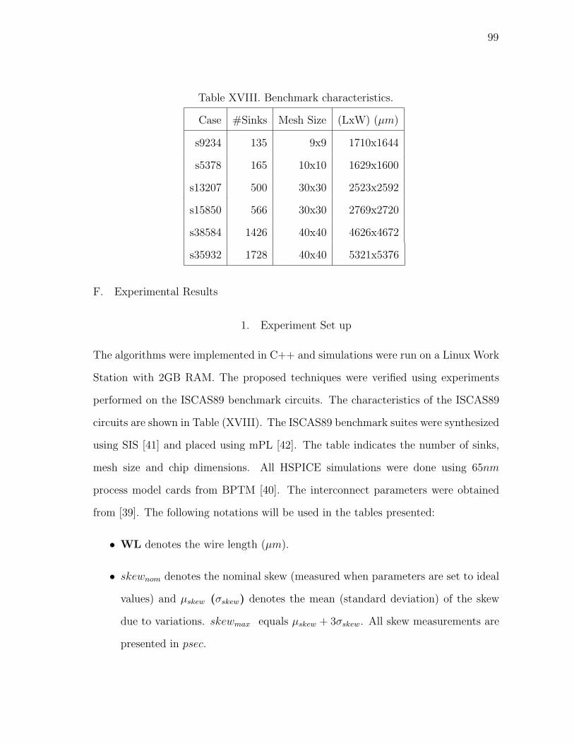
99
Table XVIII. Benchmark characteristics.
Case #Sinks Mesh Size (LxW) (µm)
s9234 135 9x9 1710x1644
s5378 165 10x10 1629x1600
s13207 500 30x30 2523x2592
s15850 566 30x30 2769x2720
s38584 1426 40x40 4626x4672
s35932 1728 40x40 5321x5376
F. Experimental Results
1. Experiment Set up
The algorithms were implemented in C++ and simulations were run on a Linux Work
Station with 2GB RAM. The proposed techniques were verified using experiments
performed on the ISCAS89 benchmark circuits. The characteristics of the ISCAS89
circuits are shown in Table (XVIII). The ISCAS89 benchmark suites were synthesized
using SIS [41] and placed using mPL [42]. The table indicates the number of sinks,
mesh size and chip dimensions. All HSPICE simulations were done using 65nm
process model cards from BPTM [40]. The interconnect parameters were obtained
from [39]. The following notations will be used in the tables presented:
• WL denotes the wire length (µm).
• skewnom denotes the nominal skew (measured when parameters are set to ideal
values) and µskew (σskew) denotes the mean (standard deviation) of the skew
due to variations. skewmax equals µskew + 3σskew. All skew measurements are
presented in psec.

100
• Pow denotes power dissipation measured in mW . The power dissipation is
measured using HSPICE simulations that measure the current drawn by the
devices in an entire clock cycle and computing the area under the voltage vs.
current curve. Hence this power includes both dynamic, leakage and crow-bar
power dissipation.
• SV (Slew Violation) is the maximum positive deviation at all the clock sink
locations from the user specified value. That is if slewr denotes the required
slew and slewmax denotes the maximum slew among the sink nodes, then:
SV = 100 ∗ (slewmax − slewr)
slewr
(5.4)
If the slew violation is negative, then it is set to zero. The slewr is set to
150psec.
• Pdelay measures the maximum permissible delay as defined by equation (5.1).
Pdelay measurements are presented in psec.
2. Experiment Design
In this work, we propose the following techniques:
1. Simultaneous mesh buffer placement/sizing.
2. Mesh reduction.
In order to measure the effectiveness of the above mentioned techniques, we conducted
the following experiments:
• Compare our mesh buffer placement/sizing algorithm with uniform sizing. By
uniform sizing, we mean placing buffer of single size uniformly distributed

101
throughout the mesh. We do the experiments for small, medium and large
buffer sizes from the library.
• Compare our mesh reduction with that of complete mesh.
We make comparisons in terms of wire length, power dissipation, nominal skew and
variation skew. For measuring the impact of variation on clock skew, we constructed
a zero skew buffered clock tree to drive the clock mesh. The clock tree construction
follows the techniques presented in [31].
For Monte Carlo simulations, the following parameters were varied (a) buffer
channel length (b) interconnect wire width (c) VDD and (d) sink load capacitance.
The above parameters are varied with mean as the nominal value and the σ value set
to 5% of the nominal value. Spatial correlation among all the variations was accounted
by using the Principal Component Analysis [29]. The Monte Carlo simulations were
done using HSPICE.
3. Results
The results for our mesh simultaneous buffer placement/sizing algorithm (henceforth
referred to as sizing algorithm) is shown in Table (XIX). The second, third and fourth
columns indicate the total buffer area, wire length and power dissipation respectively.
Buffer area is reported in terms of the buffer area of a minimum size inverter (that is,
if the buffer area is 100, then the actual buffer area is 100x times the active area of a
minimum size inverter). In the next column, we report the nominal skew. This is fol-
lowed by a set of three columns that denote mean, standard deviation and maximum
skew due to variations (obtained by running 1000 Monte Carlo simulations). The last
three columns denote the Slew Violation (computed using Equation (5.4)), maximum
permissible delay and CPU time respectively. Pdelay is computed by subtracting the

102
clock period (assuming 1GHz clock) with skewmax. The following conclusions can be
drawn from Table (XIX).
• Our sizing algorithm meets the slew specifications (within 2.5% on an average).
• The run time of our algorithm is within a few seconds and is therefore largely
inconsequential.
We compare our approach with the one where identical buffers were placed at
symmetric nodes in the mesh. Tables (XX), (XXI) and (XXII) present the nominal,
variation skew area, power and Pdelay values when the smallest, medium size and
largest buffer sizes are used to drive the mesh at symmetric nodes respectively. The
tables also provide the ratio comparison (of area, power and Pdelay) between uniform
sizing and our sizing algorithm (results in Table (XIX)). It is worth noting that the
skew results (both nominal and variation) from our sizing algorithm is not very dif-
ferent (within 15psec) from the ones obtained by using uniform sizing. The following
inferences can be made:
• Using the smallest buffer uniformly results in an area reduction of 37% compared
to our sizing algorithm. However, it also leads to 33% slew violation on an
average and up to 77% in some cases. Pdelay values are identical for almost all
the approaches.
• Medium buffer sizes satisfy slew constraints in all but one case and large buffer
size satisfies the slew constraints in all the cases. But, this comes at an area
penalty of 21% (46%) for medium (large) buffer size.
Figures (25,26,27) gives the worst case output signal (signal at the sink that has
the worst slew) while using small, medium, large buffer sizes. Figure (28) gives the
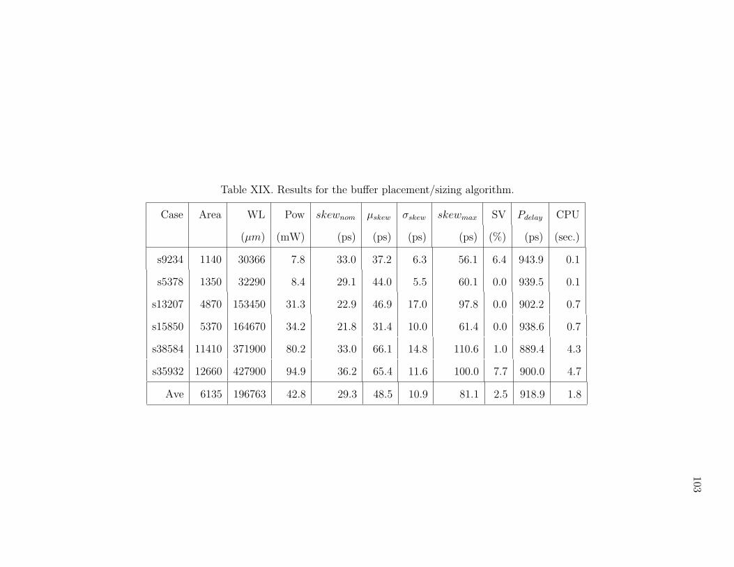
103
Table XIX. Results for the buffer placement/sizing algorithm.
Case Area WL Pow skewnom µskew σskew skewmax SV Pdelay CPU
(µm) (mW) (ps) (ps) (ps) (ps) (%) (ps) (sec.)
s9234 1140 30366 7.8 33.0 37.2 6.3 56.1 6.4 943.9 0.1
s5378 1350 32290 8.4 29.1 44.0 5.5 60.1 0.0 939.5 0.1
s13207 4870 153450 31.3 22.9 46.9 17.0 97.8 0.0 902.2 0.7
s15850 5370 164670 34.2 21.8 31.4 10.0 61.4 0.0 938.6 0.7
s38584 11410 371900 80.2 33.0 66.1 14.8 110.6 1.0 889.4 4.3
s35932 12660 427900 94.9 36.2 65.4 11.6 100.0 7.7 900.0 4.7
Ave 6135 196763 42.8 29.3 48.5 10.9 81.1 2.5 918.9 1.8
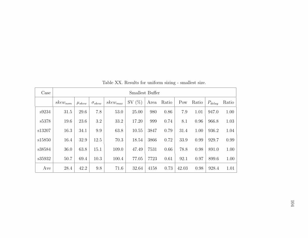
104
Table XX. Results for uniform sizing - smallest size.
Case Smallest Buffer
skewnom µskew σskew skewmax SV (%) Area Ratio Pow Ratio Pdelay Ratio
s9234 31.5 29.6 7.8 53.0 25.00 980 0.86 7.9 1.01 947.0 1.00
s5378 19.6 23.6 3.2 33.2 17.20 999 0.74 8.1 0.96 966.8 1.03
s13207 16.3 34.1 9.9 63.8 10.55 3847 0.79 31.4 1.00 936.2 1.04
s15850 16.4 32.9 12.5 70.3 18.54 3866 0.72 33.9 0.99 929.7 0.99
s38584 36.0 63.8 15.1 109.0 47.49 7531 0.66 78.8 0.98 891.0 1.00
s35932 50.7 69.4 10.3 100.4 77.05 7723 0.61 92.1 0.97 899.6 1.00
Ave 28.4 42.2 9.8 71.6 32.64 4158 0.73 42.03 0.98 928.4 1.01

105
Table XXI. Results for uniform sizing - medium buffer size.
Case Medium Buffer
skewnom µskew σskew skewmax SV (%) Area Ratio Pow Ratio Pdelay Ratio
s9234 25.6 25.3 7.0 46.2 0.00 1642 1.44 8.4 1.08 953.8 1.01
s5378 21.5 23.0 3.4 33.2 0.00 1661 1.23 8.7 1.04 966.8 1.03
s13207 14.6 35.6 9.9 65.2 0.00 6380 1.31 32.7 1.04 934.8 1.04
s15850 14.9 40.7 13.6 81.4 0.00 6390 1.19 35.2 1.03 918.6 0.98
s38584 28.3 61.3 14.8 105.7 0.00 12551 1.10 81.5 1.02 894.4 1.01
s35932 39.3 68.7 13.6 109.3 13.23 12787 1.01 95.3 1.00 890.7 0.99
Ave 24.0 42.4 10.4 73.5 2.21 7442 1.21 43.63 1.03 926.5 1.01

106
Table XXII. Results for uniform sizing - largest buffer size.
Case Largest Buffer
skewnom µskew σskew skewmax SV (%) Area Ratio Pow Ratio Pdelay Ratio
s9234 23.2 24.8 5.9 42.6 0.00 1972 1.73 8.8 1.13 957.5 1.01
s5378 17.7 21.2 3.2 30.7 0.00 1998 1.48 9.1 1.08 969.3 1.03
s13207 13.0 38.6 4.2 51.2 0.00 7695 1.58 34.1 1.09 948.8 1.05
s15850 11.9 44.8 14.6 88.7 0.00 7679 1.43 36.6 1.07 911.3 0.97
s38584 24.7 62.7 14.8 107.0 0.00 15175 1.33 75.3 0.94 893.0 1.00
s35932 34.9 69.4 13.7 110.6 0.00 15319 1.21 91.1 0.96 889.4 0.99
Ave 20.9 43.6 9.4 71.8 0.00 8955 1.46 42.50 1.05 928.2 1.01

107
corresponding plot while using our sizing algorithm. In each of the above mentioned
plots, the ideal signal output (with signal slew of 150psec) is also shown for compari-
son. The plots were obtained for the test case s35932. Notice that using large buffer
type as well as using our sizing algorithm gives a waveform that closely resembles the
ideal output. However, using large buffer size will result in 46% increase in buffer
area. Using small and medium buffer sizes gives a signal waveform that deviates
significantly from the slew specification.
Next we compare the results of the mesh reduction algorithm. We compare
both resource consumption and tolerance to variation. The results are indicated in
Table (XXIII). We present the wire length and power reduction when compared to
the complete mesh. Table (XXIII) also presents the nominal skew, mean, standard
deviation, maximum skew value and the maximum delay (Pdelay) obtained on running
Monte Carlo simulations run with the set up described earlier. The results can be
summarized as follows:
• Mesh leads to a wire length reduction of 25.9% and power savings of
18.5% on an average.
• In some test cases the power savings can be as high as 28%.
• These savings do have an impact on the tolerance to variations. However, it can
be seen that the delay penalty is less than 3.3% on all the cases. In fact, the
delay penalty is less than 1% for the two largest test cases. The nominal skew
results are identical to those obtained without reduction. Hence mesh reduction
preserves the nominal skew.
Figure (29) gives the power vs. maximum skew trade off curve for test case
s9234. The Y-axis measures the power dissipation and X-axis measures the skewmax

108
value after measuring the skew using Monte Carlo simulations. Each point in the
curve is obtained by setting a different value of k. A higher value would imply more
paths, more wire length, more power dissipation, lower skew and higher Pdelay and
vice-versa for lower k (k is the number of buffers each sink should be connected to
with paths of short length as defined in section (C)). Since our algorithm is very fast,
the user can potentially run it for different values of k and pick the one meets the
design specifications. Thus it provides a framework for trade off between skew
and power dissipation.
Table (XXIV) gives the buffer area, power and Pdelay results for the post process-
ing technique detailed in section (2). The table also compares the results with those
shown in Table (XXIII. The following inferences can be drawn from Table (XXIV).
Post processing technique can be treated as a fine tuning technique and not an opti-
mization procedure of its own. However, it does result in 3.8% reduction in buffer
area (and could be as high 9.9%) on an average. Such a reduction though small could
be significant in high performance designs. Post-processing does not have much of an
impact on power dissipation and permissible delay.
Fig. 25. Worst case output waveform with small buffer size.

109
Fig. 26. Worst case output waveform with medium buffer size.
Fig. 27. Worst case output waveform with large buffer size.
Fig. 28. Worst case output waveform with sizing algorithm.

110
Table XXIII. Results for mesh reduction.
Case Wire Length Pow skewnom µskew σskew skewmax Pdelay
µm % Imp. mW % Imp (ps) (ps) (ps) (ps) (ps) % Red
s9234 27177 10.5 6.7 6.1 33.0 45.4 7.8 68.7 931.3 1.3
s5378 24911 22.9 6.7 14.0 29.1 44.7 6.4 63.8 936.2 0.3
s13207 109538 28.6 23.8 21.5 22.9 60.0 22.5 127.5 872.5 3.3
s15850 100778 38.8 23.8 28.1 21.8 37.5 11.3 71.2 928.8 1.0
s38584 262528 29.4 60.9 22.0 33.0 70.5 16.0 118.5 881.5 0.9
s35932 321293 24.9 74.3 19.6 36.2 71.2 12.3 108.1 891.9 0.9
Ave 131981 25.9 32.7 18.5 29.7 54.9 12.7 93.0 907.0 1.3

111
5
5.5
6
6.5
7
7.5
50 60 70 80 90 100 110
Pow
er d
issi
patio
n (m
W)
Maximum skew (psec)
Power skew trade off
Fig. 29. Power vs. skewmax trade off for s9234
Table XXIV. Reduction in buffer area and power after post-processing.
Case Buffer Area Imp (%) Pow Imp(%) Pdelay Imp(%)
s9234 1100 3.5 7.35 0.68 931.3 0.0
s5378 1350 0.0 7.42 0.00 936.1 0.0
s13209 4740 2.7 24.48 0.41 872.5 0.0
s15850 4840 9.9 23.98 2.12 928.8 0.0
s38584 10880 4.7 63.20 0.88 881.5 0.0
s35932 12660 1.8 78.51 0.24 891.9 0.0
Ave 5890 3.8 34.16 0.72 907.0 0.0

112
CHAPTER VI
CONCLUSIONS
We presented several techniques for two key problems in clock distribution networks:
(a) Skew degradation due to PVT variations and (b) Power dissipation. Our tech-
niques have been tested through extensive experimentation.
For tree based distributions, we integrated skew scheduling, topology generation
and layout embedding into one framework - reduce maximum skew due to variations.
In the proposed skew scheduling algorithm, process variations were considered directly
in skew safety margin allocations so that a larger safety margin can be obtained for
registers far apart. In the clock routing algorithm, a new layout embedding technique
was developed to optimally minimize the maximum skew violation due to process
variations. The effectiveness of the proposed algorithms was validated through Monte
Carlo simulations on benchmark circuits. Experimental results indicate that our
techniques can reduce the maximum skew violation by 19% on an average.
Link insertion has been shown to be an effective technique to reduce the clock
skew due to variations with minimal increase in wire length. However, previous works
on link insertion were restricted to unbuffered clock nets. In reality, buffers are needed
to meet signal delay and slew constraints. We addressed the issues/risks involved in
inserting links in buffered clock nets. A design criteria to avoid the short-circuit
current was detailed. Link insertion works under the assumption that a low skew
tree is available as input. We detail techniques to produce low skew trees under a
higher order delay model. The tree generated is friendly towards link insertion. The
effectiveness of link insertion was demonstrated via Monte Carlo simulations that
considered all major source of variations. The simulations also took care of spatial
correlations between the sources of variations. We compared our technique with both

113
tree and mesh (a popular form of non-tree based clock distribution). Experimental
results indicate that our technique can be used to reduce the skew by over 32% with
less than 5% increase in power dissipation.
Rotary clocking is a promising new clocking scheme that handles both power
dissipation and skew variation simultaneously. We detailed the issues involved in
adopting current CAD flow towards rotary clocking. Based on the problem specific
constraints, we presented an alternative flow and algorithms. The proposed flow
integrates clock skew optimization with placement. By utilizing intentional skew
management and flip-flop clustering, both the phase and physical location constraints
of the rotary clocking can be satisfied. We also proposed techniques to minimize the
maximum load capacitance seen by the rotary rings. To the best of our knowledge, this
is the first placement and skew optimization work for rotary clocking. Experimental
results indicate that our techniques can reduce the tapping cost by 37%-52% with
2.6%-6% reduction in total wirelength. Since our method enables a concurrent clock
network and placement design, it is potentially useful for other clocking methodologies
like [62] as well. In our current methodology, we connect the ring directly to the flip-
flops assigned to them. However, this could be improved by creating local trees that
connect the ring location to a set of flip-flops. In such a construction, care should
be taken to take care of the skew permissible ranges of the flip-flop pairs. Such a
scheme could lead to potential benefits in wirelength and power dissipation. Further,
our formulations take the number of rotary rings as part of the input. A better
approach would be to integrate the number of rings as a variable in our methodology.
This could lead to better optimization as it increases the solution space. We wish to
investigate both these aspects in our future work.
Clock mesh is a very popular form of CDN among high performance systems.
We addressed some key issues involved in the design and optimization of clock mesh.

114
We detailed a mesh buffer sizing/placement algorithms that places and sizes the mesh
buffers in order to meet the signal slew constraints while minimizing the buffer cost.
Clock mesh is tolerant towards variations in clock skew. The tolerance comes at the
expense of redundancy created due to the multiple paths between the mesh buffers
and the clock sinks. Such a redundancy also results in high power dissipation. We
formulate the problem of mesh reduction by using concepts from survivable network
theory. We remove selective number of mesh edges thereby trading off skew tolerance
for lower power dissipation. The number of edges removed depends upon user defined
parameters. Depending on these parameters the user can choose to remove large
(implies low skew tolerance and low power) number of edges or small number of edges
(implies high skew tolerance and high power). Our technique for mesh reduction is
fast. Hence, the user can run the algorithm for different parameter values and choose
the desired trade-off point. Our techniques indicate up to 28% reduction in power
with less than 3.3% increase in maximum permissible delay.

115
REFERENCES
[1] J. P. Fishburn, “Clock skew optimization”, IEEE Transactions on Computers,
vol. 39, no. 7, pp. 945–950, 1990.
[2] Y. Liu, S. R. Nassif, L. T. Pileggi, and A. J. Strojwas, “Impact of interconnect
variations on the clock skew of a gigahertz microprocessor”, IEEE/ACM Design
Automation Conference, pp. 168–171, 2000.
[3] P. Saxena, N. Menezes, P. Cocchini and D. A. Kirkpatrick, “Repeater scaling and
its impact on CAD”, IEEE Transactions Computer-Aided Design of Integrated
Circuits and Systems, vol. 23, no. 4, pp. 451–463, 2004.
[4] R. Saleh, S. Z. Hussain, S. Rochel and D. Overhauser, “Clock skew verification
in the presence of IR-drop in the power distribution network”, IEEE Transac-
tions Computer-Aided Design of Integrated Circuits and Systems, vol. 19, no. 6,
pp. 635–644, 2000.
[5] W. Liao and L. He, “Full-Chip interconnect power estimation and simulation
considering concurrent repeater and flip-flop insertion”, IEEE/ACM Interna-
tional Conference on Computer-Aided Design, pp. 574–580, 2003.
[6] V. Tiwari, D. Singh, S. Rajagopal, G. Mehta, R. Patel and F. Baez, “Reducing
power in high-performance microprocessors”, IEEE/ACM Design Automation
Conference, pp. 732–737, 1998.
[7] C.-W. A. Tsao and C.-K. Koh, “UST/DME: a clock tree router for general skew
constraints”, ACM Transactions on Design Automation of Electronic Systems,
vol. 7, no. 3, pp. 359–379, 2002.

116
[8] A. Rajaram, J. Hu, and R. Mahapatra, “Reducing clock skew variability via
cross links”, IEEE/ACM Design Automation Conference, pp. 18–23, 2004.
[9] A. Rajaram, D. Pan, and J. Hu, “Improved algorithms for link based non-tree
clock network for skew variability reduction”, ACM International Symposium
on Physical Design, pp. 55–62, 2005.
[10] J. Wood, T. C. Edwards, and S. Lipa, “Rotary traveling-wave oscillator arrays:
a new clock technology”, IEEE Journal of Solid-State Circuits, vol. 36, no. 11,
pp. 1654–1665, November 2001.
[11] G. Northrop, G. Averill, R. Barkley, K. Carey, S. Chan, et al., “609 MHz G5
S/399 microprocessor”, International Solid-State Circuits Conference, pp. 88–89,
1999.
[12] P. J. Restle, C. A. Carter, J. P. Eckhardt, B. L. Krauter, B. D. McCredie, et al.,
“The clock distribution of the Power4 microprocessor”, International Solid-State
Circuits Conference, pp. 144–145, 2002.
[13] R. Heald. “Implementation of a 3rd-generation SPARC V9 64 b microprocessor”,
International Solid-State Circuits Conference, pp. 412–413, 2000.
[14] B. Lu, J. Hu, G. Ellis, and H. Su, “Process variation aware clock tree routing”,
ACM International Symposium on Physical Design, pp. 174–181, 2003.
[15] W. C. Elmore, “The transient analysis of damped linear networks with particular
regard to wideband amplifiers”, Journal of Applied Physics, vol. 19, no. 1, pp.
55–63, 1948.
[16] J. Rubinstein, P. Penfield, and M. A. Horowitz, “Signal delay in RC tree net-
works”, IEEE Transactions on Computer-Aided Design of Integrated Circuits

117
and Systems, CAD vol. 2, no. 3, pp. 202–211, July 1983.
[17] T.-H. Chao, Y.-C. Hsu, J.-M.Ho, K. D. Boese and A. B. Kahng, “Zero skew
clock routing with minimum wirelength”, IEEE Transactions on Circuits and
Systems-II, vol. 39, no. 39, pp. 799–814, 1992.
[18] R. S. Tsay. “An exact zero-skew clock routing algorithm”, IEEE Transactions
Computer-Aided Design of Integrated Circuits and Systems, vol. 12, no. 2, pp.
242–249, 1993.
[19] R. B. Deokar and S. S. Sapatnekar, “A graph-theoretic approach to clock skew
optimization”, International Symposium of Circuits and Systems, pp. 407–410,
1994.
[20] M. Edahiro, “A clustering-based optimization algorithm in zero-skew routings”,
IEEE/ACM Design Automation Conference, pp. 612–616, 1993.
[21] D. Velenis, M. C. Papaefthymiou, and E. G. Friedman, “Reduced delay uncer-
tainty in high performance clock distribution networks”, Design Automation and
Test Europe, pp. 68–73, 2003.
[22] R. Chaturvedi and J. Hu, “A simple yet effective merging scheme for prescribed-
skew clock routing”, International Conference on Computer Design, pp. 282-287,
2003.
[23] C. Albrecht, B. Korte, J. Schietke, and J. Vygen, “Cycle time and slack optimiza-
tion for VLSI-chips”, IEEE/ACM International Conference on Computer-Aided
Design, pp. 232–238, 1999.
[24] I. S. Kourtev and E. G. Friedman, “Clock skew scheduling for improved reli-
ability via quadratic programming”, IEEE/ACM International Conference on

118
Computer-Aided Design, pp. 239–243, 1999.
[25] N. Bindal, T. Kelly, N. Velastegui, and K. L. Wong, “Scalable sub-10ps skew
global clock distribution for a 90nm multi-GHz IA microprocessor”, IEEE In-
ternational Solid-State Circuits Conference, pp. 346–355, 2003.
[26] S. Zanella, A. Nardi, A. Neviani, M. Quarantelli, S. Saxena, and C. Guardiani,
“Analysis of the impact of process variations on clock skew”, IEEE Transactions
on Semiconductor Manufacturing, vol. 13, no. 4, pp. 401–407, November 2000.
[27] R. Saleh, S. Z. Hussain, S. Rochel, and D. Overhauser, “Clock skew verification
in the presence of IR-drop in the power distribution network”, IEEE Transac-
tions on Computer-Aided Design, vol. 19, no. 6, pp. 635–644, June 2000.
[28] C. Visweswariah, “Death, taxes and failing chips”, IEEE/ACM Design Automa-
tion Conference, pp. 343–347, 2003.
[29] H. Chang and S. S. Sapatnekar, “Statistical timing analysis considering spatial
correlations using a single PERT-like traversal”, IEEE/ACM Int Conference on
Computer Aided Design , pp. 621–625, 2003.
[30] A. Rajaram, D. Z. Pan, “Variation tolerant buffered clock network synthesis with
cross links”, ACM International Symposium oh Physical Design, pp. 157–164,
2006.
[31] G. Venkataraman, N. Jayakumar, J. Hu, P. Li, S. Khatri, A. Rajaram,
P. McGuinness and C. Alpert, “Practical techniques to reduce skew and its
variations in buffered clock networks”, IEEE/ACM International Conference on
Computer Aided Design, pp. 592–596, 2005.

119
[32] J. Wyatt, “Signal delay in RC mesh networks”, IEEE Transactions on
Computer-Aided Design, vol. 32, no. 5, pp. 507–510, May 2005.
[33] J. L. Tsai, D. Baik, C. C. Chen and K. Saluja, “A yield improvement methodol-
ogy using pre- and post-silicon statistical clock scheduling”, IEEE/ACM Inter-
national Conference on Computer Aided Design, pp. 611–618, 2004.
[34] S. Pullela, N. Menezes, J. Omar, and L. T. Pillage, “Skew and delay optimiza-
tion for reliable buffered clock trees”, IEEE/ACM International Conference on
Computer-Aided Design, pp. 556–562, 1993.
[35] J. G. Xi and W. W.-M. Dai, “Buffer insertion and sizing under process variations
for low power clock distribution”, IEEE/ACM Design Automation Conference,
pp. 491–496, 1995.
[36] X. Zeng, D. Zhou, and W. Li, “Buffer insertion for clock delay and skew mini-
mization”, ACM International Symposium on Physical Design, pp. 36–41, 1999.
[37] R. Chaturvedi and J. Hu, “Buffered clock tree for high quality IC design”, IEEE
International Symposium on Quality Electronic Design, pp. 381–386, 2004.
[38] K. Wang and M. Marek-Sadowska, “Clock network sizing via sequential linear
programming with time-domain analysis”, ACM International Symposium on
Physical Design, pp. 182–189, 2004.
[39] A. B. Kahng and B. Liu. ”Q-Tree: A new iterative improvement approach for
buffered interconnect optimization”, IEEE Comp. Soc. Annual Symp. On VLSI,
pp. 183-188, February, 2003.
[40] Y. Cao. “Predictive Technology Model”, Nanoscale integration and mod-
eling group, Arizona State Univerity, Downloaded on April 2, 2006 from

120
http://www.eas.asu.edu/∼ptm/.
[41] E. M. Sentovich, K. J. Singh, L. Lavagno, C. Moon, R. Murgai, A. Saldanha,
H. Savoj, P. R. Stephan, R. K. Brayton, and A. L. Sangiovanni-Vincentelli,
“SIS: a system for sequential circuit synthesis”, Memorandum no. M92/41, ERL,
University of California, Berkeley, May 1992.
[42] “CPMO-constrained placement by multilevel optimization”, Computer
Science Department, UCLA, Downloaded on March 1, 2005 from
http://cadlab.cs.ucla.edu/cpmo/mpl.
[43] R. O’Mahony, C. P. Yue, M. A. Horowitz, and S. S. Wong, “A 10-GHz global
clock distribution using coupled standing-wave oscillators”, IEEE Journal of
Solid-State Circuits, vol. 38, no. 11, pp. 1813–1820, November 2003.
[44] S. C. Chan, K. L. Shepard, and P. J. Restle, “Uniform-phase uniform-amplitude
resonant-load global clock distributions”, IEEE Journal of Solid-State Circuits,
vol. 40, no. 1, pp. 102–109, January 2005.
[45] Z. Yu and X. Liu, “Power analysis of rotary clock”, IEEE Computer Society
Annual Symposium on VLSI, pp. 150–155, 2005.
[46] S. Held, B. Korte, J. Maβberg, M. Ringe, and J. Vygen, “Clock scheduling and
clock tree construction for high performance ASICs”, IEEE/ACM International
Conference on Computer-Aided Design, pp. 232–239, 2003.
[47] H. Eisenmann and F. M. Johannes, “Generic global placement and floorplan-
ning”, IEEE/ACM Design Automation Conference, pp. 269–274, 1998.
[48] T. F. Chan, J. Cong, J. Shinnerl, and K. Sze, “An enhanced multilevel algorithm
121
for circuit placement”, IEEE/ACM International Conference on Computer-
Aided Design, pp. 299–306, 2003.
[49] R. K. Ahuja, T. L. Magnanti, and J. B. Orlin, Network Flows: Theory, Algo-
rithms, and Applications. Upper Saddle River, NJ:Prentice Hall, 1993.
[50] P. J. Restle, T. G. McNamara, D. A. Webber, P. J. Camporese, K. F. Eng, K. A.
Jenkins, D. H. Allen, M. J. Rohn, M. P. Quaranta, D. W. Boerstler, C. J. Alpert,
C. A. Carter, R. N. Bailey, J. G. Petrovick, B. L. Krauter, and B. D. McCredie,
“A clock distribution network for microprocessors”, IEEE Journal of Solid-State
Circuits, vol. 36, no. 5, pp. 792–799, May 2001.
[51] V. V. Vazirani, Approximation Algorithms, New York:Springer 2001.
[52] “GNU linear programming kit”, Downloaded on December 15, 2005 from
http://www.gnu.org/software/glpk/glpk.html.
[53] R. Wunderling, “Paralleler und Objektorientierter Simplex-Algorithmus”, ZIB
Technical Report TR 96-09, Berlin, 1996.
[54] C. J. Alpert, J. Hu, S. S. Sapatnekar and C. N. Sze, “Accurate estimation of
global buffer delay within a floorplan”, IEEE Transactions on Computer-Aided
Design, vol. 25, no. 6, pp. 1140–1145, June 2006.
[55] N. A. Kurd, J. S. Barkatullah, R. O. Dizon, T. D. Fletcher, and P. D. Madland,
“A multigigahertz clocking scheme for the Pentium 4 microprocessor”, IEEE
Journal of Solid-State Circuits, vol. 36, no. 11, pp. 1647–1653, November 2001.
[56] H. Su and S. Sapatnekar, “Hybrid structured clock network construction”, In-
ternational Conference on Computer-Aided Design, pp., 333–336, 2001.

122
[57] M. Donno, Enrico Macii and L. Mazzoni, “Power aware clock tree planning”,
ACM International Symposium on Physical Design, pp. 138–147, 2004.
[58] U. Feige, “A threshold of ln(n) for approximating set cover”, Journal of ACM,
vol. 45, no. 4, pp. 634–652, 1998.
[59] K. Jain, “A factor 2 approximation algorithm for the generalized steiner network
problem”, IEEE Symposium on Foundations of Computer Science, pp. 448–457,
1998.
[60] H. Kerivin and A. R. Mahjoub, “Design of survivable networks: A survey”,
Networks, vol. 46, no. 1, pp. 1–21, April 2005.
[61] W Ben-Ameur, “Constrained length connectivity and survivable networks”,
Networks, vol. 36, no. 1, pp. 17–23, August 2000.
[62] Y. Lu, C. N. Sze, X. Hong, Q. Zhou, Y. Cai, L. Huang, and J. Hu, “Navigating
registers in placement for clock network minimization”, IEEE/ACM Design
Automation Conference, pp. 176–181, 2005.

123
VITA
Ganesh Venkataraman received his B. E. (Hons) Electrical and Electronics and
M. Sc. (Hons) Physics from the Birla Institute of Technology and Science, Pilani,
India in 2000. He completed his M. S. in Electrical and Computer Engineering from
the University of Iowa in the year 2003.
Ganesh worked as Design Engineer at Cypress Semiconductor between June 2000
and June 2001. He worked as a summer intern at Intel (summer 2005) and IBM Austin
Research Lab (2006).
His research interests include VLSI physical design, variation tolerant clock dis-
tributions, low power, placement, routing, gate sizing, graph theory and combinato-
rial optimization. His works have been published in leading international conferences
including International Conference of Computer-Aided Design (ICCAD), Asia and
South Pacific Design Automation Conference (ASPDAC), Design Automation and
Test Europe (DATE) and Symposium on Discrete Algorithms (SODA).
Ganesh received the Graduate Merit Fellowship from Texas A&M University.
This fellowship is awarded via university wide competition among incoming graduate
students. He received the Government Merit Scholarship in the year 1993 and 1995.
This is awarded by the Government of India to the 0.1% of the 100,000+ students
who took the 10th and 12th standard CBSE examinations in the year 1993 and 1995
respectively. He was the President of the Association for India’s Development (AID)
TAMU chapter in the year 2005-06.
Ganesh can be reached at the Department of Electrical and Computer Engineer-
ing, 333 WERC, Texas A&M University, TX - 77843.
The typist for this dissertation was Ganesh Venkataraman.