Embed Size (px)
Citation preview

CMOS VLSI For Computer Engineering
Lecture 8: Clock Distribution, PLL & DLL
Parts adapted from http://www3.hmc.edu/~harris/cmosvlsi/
4e/index.html

CMOS VLSI for Computer Engineering
2
Clock Distribution
• On a small chip, the clock distribution network is just a wire And possibly an inverter for clkb
• On practical chips, the RC delay of the wire resistance and gate load is very long Variations in this delay cause clock to get to different
elements at different times This is called clock skew
• Most chips use repeaters to buffer the clock and equalize the delay Reduces but doesn’t eliminate skew

CMOS VLSI for Computer Engineering
3
Example
• Skew comes from differences in gate and wire delay With right buffer sizing, clk1 and clk2 could ideally arrive at
the same time. But power supply noise changes buffer delays clk2 and clk3 will always see RC skew
3 mm
1.3 pF
3.1 mmgclk
clk1
0.5 mm
clk2clk3
0.4 pF 0.4 pF

CMOS VLSI for Computer Engineering
4
Review: Skew Impact
F1
F2
clk
clk clk
Combinational Logic
Tc
Q1 D2
Q1
D2
tskew
CL
Q1
D2
F1
clk
Q1
F2
clk
D2
clk
tskew
tsetup
tpcq
tpdq
tcd
thold
tccq
setup skew
sequencing overhead
hold skew
pd c pcq
cd ccq
t T t t t
t t t t
• Ideally full cycle is
available for work
• Skew adds sequencing
overhead
• Increases hold time too

CMOS VLSI for Computer Engineering
5
Solutions
• Reduce clock skew Careful clock distribution network design Plenty of metal wiring resources
• Analyze clock skew Only budget actual, not worst case skews Local vs. global skew budgets
• Tolerate clock skew Choose circuit structures insensitive to skew

CMOS VLSI for Computer Engineering
6
Clock Dist. Networks
• Ad hoc
• Grids
• H-tree
• Hybrid

CMOS VLSI for Computer Engineering
7
Clock Grids
• Use grid on two or more levels to carry clock
• Make wires wide to reduce RC delay
• Ensures low skew between nearby points
• But possibly large skew across die
CMOS VLSI for Computer Engineering
8
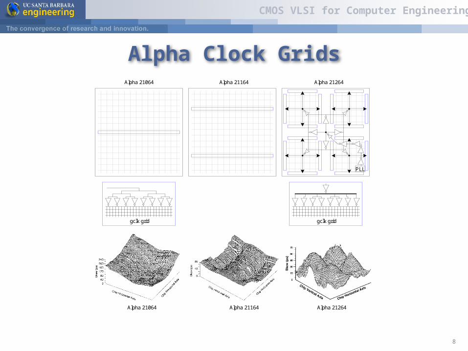
Alpha Clock Grids
PLL
gclk grid
Alpha 21064 Alpha 21164 Alpha 21264
gclk grid
Alpha 21064 Alpha 21164 Alpha 21264

CMOS VLSI for Computer Engineering
9
H-Trees
• Fractal structure Gets clock arbitrarily close to any point Matched delay along all paths
• Delay variations cause skew
• A and B might see big skew A B

CMOS VLSI for Computer Engineering
10
Itanium 2 H-Tree
• Four levels of buffering: Primary driver Repeater Second-level
clock buffer Gater
• Route around
obstructions
Primary Buffer
Repeaters
Typical SLCBLocations

CMOS VLSI for Computer Engineering
11
Pentium 4 Clock Grid

CMOS VLSI for Computer Engineering
12
Recent Microprocessor Skews

CMOS VLSI for Computer Engineering
13
Hybrid Networks
• Use H-tree to distribute clock to many points
• Tie these points together with a grid
• Ex: IBM Power4, PowerPC H-tree drives 16-64 sector buffers Buffers drive total of 1024 points All points shorted together with grid

CMOS VLSI for Computer Engineering
14
Clock Generation
• Low frequency: Buffer input clock and drive to all registers
• High frequency Buffer delay introduces large skew relative to input clocks
• Makes it difficult to sample input data
Distributing a very fast clock on a PCB is hard

CMOS VLSI for Computer Engineering
15
Zero-Delay Buffer
• If the periodic clock is delayed by Tc, it is indistinguishable from the original clock
• Build feedback system to guarantee this delay
Phase-Locked Loop (PLL)
Delay-Locked Loop (PLL)

CMOS VLSI for Computer Engineering
16
Frequency Multiplication
• PLLs can multiply the clock frequency

CMOS VLSI for Computer Engineering
17
Phase and Frequency
• Analyze PLLs and DLLs in term of phase F(t) rather than voltage v(t)
• Input and output clocks may
deviate from locked phase Small signal analysis
1 mod 2clk
0 mod 2
t
t
0
2t
t f t dt
in in
out out
t t t
t N t t

CMOS VLSI for Computer Engineering
18
Linear System Model
• Treat PLL/DLL as a linear system Compute deviation DF from locked position Assume small deviations from locked Treat system as linear for these small changes
• Analysis is not valid far from lock e.g. during acquisition at startup
• Continuous time assumption PLL/DLL is really a discrete time system
• Updates once per cycle If the bandwidth << 1/10 clock freq, treat as continuous
• Use Laplace transforms and standard analysis of linear continuous-time feedback control systems

CMOS VLSI for Computer Engineering
19
Phase-Locked Loop (PLL)
• System
• Linear Model

CMOS VLSI for Computer Engineering
20
Voltage-Controlled Oscillator
• VCO
ctrl ctrl0 ctrl
ctrl
2
outvco
out vco
ctrl
V t V V t
fK
V
s K
V s s

CMOS VLSI for Computer Engineering
21
Alternative Delay Elements

CMOS VLSI for Computer Engineering
22
Frequency Divider
• Divide clock by N Use mod-N counter
outfb
outfb
ff
N
N

CMOS VLSI for Computer Engineering
23
Phase Detector
• Difference of input and
feedback clock phase
• Often built from phase-frequency detector (PFD)

CMOS VLSI for Computer Engineering
24
Phase Detector
• Convert up and down pulses into current proportional to phase error using a charge pump
cp
err 2pd
pd
I s IK
s

CMOS VLSI for Computer Engineering
25
Loop Filter
• Convert charge pump
current into Vctrl
• Use proportional-integral control (PI) to generate a control signal dependent on the error and its integral Drives error to 0
ctrl
pd
1V sR
I s sC (negligible)

CMOS VLSI for Computer Engineering
26
PLL Loop Dynamics
• Closed loop transfer function of PLL
• This is a second order system
• wn indicates loop bandwidth
• z indicates damping; choose 0.7 – 1 to avoid ringing
vco
out
vcoin
21
21 11
pd
pd
KK R
s sC sH s
Ks K RN sC s
vco
2
2 2
2
2
2
cpn
n n
n n n
I Ks NCH s N
s sRC

CMOS VLSI for Computer Engineering
27
Delay Locked Loop
• Delays input clock rather than creating a new clock with an oscillator
• Cannot perform frequency multiplication
• More stable and easier to design 1st order rather than 2nd
• State variable is now time (T) Locks when loop delay is exactly Tc
Deviations of DT from locked value

CMOS VLSI for Computer Engineering
28
Delay-Locked Loop (DLL)
• System
• Linear Model
CMOS VLSI for Computer Engineering
29
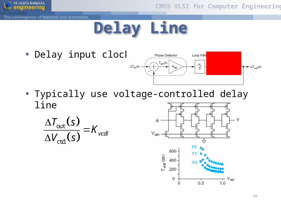
Delay Line
• Delay input clock
• Typically use voltage-controlled delay line
out
ctrlvcdl
T sK
V s

CMOS VLSI for Computer Engineering
30
Phase Detector
• Detect phase error
• Typically use PFD and charge pump, as in PLL
err
pd cp
c
I s I
T s T

CMOS VLSI for Computer Engineering
31
Loop Filter
• Convert error current
into control voltage
• Integral control is sufficient
• Typically use a capacitor as the loop filter
ctrl 1I
pd
V s K
I s s sC

CMOS VLSI for Computer Engineering
32
DLL Loop Dynamics
• Closed loop transfer function of DLL
• This is a first order system
• t indicates time constant (inverse of bandwidth) Choose at least 10Tc for continuous time approx.
out
in
1
1
T sH s
T s s
1 c
pd I vcdl cp vcdl
CT
K K K I K