Embed Size (px)
Citation preview

ELECTRONICS & COMMUNICATION ENGG V SEMESTER COURSE DIARY
PAGE 1 MVJCE
V SEMESTER

ELECTRONICS & COMMUNICATION ENGG V SEMESTER COURSE DIARY
PAGE 2 MVJCE
06XX-51: Entrepreneurship Development and Management

ELECTRONICS & COMMUNICATION ENGG V SEMESTER COURSE DIARY
PAGE 3 MVJCE
SYLLABUS
Sub Code : 06XX51 I A Marks: 25 Hours / Week: 4 Exam Marks: 100 Total Hours: 52 Exam Hours: 03
Part A Unit 1
Entrepreneurship: Concept, meaning, need and Competencies/qualities/traits of an entrepreneur, technopreneurship. 5 Hrs Innovation:Introduction, Motivating to innovate, Introduce core ideas about how to think about innovation, including key theories about factors that affect innovation. An in depth review of how companies structure to encourage and develop innovation. Product development and design.
5 Hrs Unit 2
Role of financial institutions in entrepreneurship development Role of financial institutions in entrepreneurship development like District Industry Centres (DICs), State Financial Corporations, Small Industries Service Institutes (SISIs), Small Industries Development, Bank of India (SIDBI), National Small Industries Corporation (NSIC) and other relevant institutions/organizations. 6 Hrs
Unit 3 Market Survey and Opportunity Identification (Business Planning) :How to start an industry, procedures for registration of industry, assessment of demand and supply, in potential areas of growth, understanding business opportunity, considerations in product selection, data collection for setting up new ventures 6 Hrs
Unit 4 Legal Aspects of Small Business: Elementary knowledge of Income Tax, Sales Tax, Patent Rules, Excise Rules, Factory Act and Payment of Wages Act. Knowledge of Government policies to promote entrepreneurship like SEZ, technology parks etc. 4 Hrs
Part B Unit 5
Introduction to Engineering Management: Engineering and Management, historical development of engineering management. 4 Hrs
Unit 6 Functions of technology management: planning and forecasting, decision making, organizing, motivating and leading technical people, controlling. 13 Hrs
Unit 7 Managing projects: Project planning and acquisition, project organization, leadership and control. 6 Hrs
Unit 8 Project Report Preparation: Preliminary report, Techno-economic feasibility report, Project viability. 4 Hrs

ELECTRONICS & COMMUNICATION ENGG V SEMESTER COURSE DIARY
PAGE 4 MVJCE
Text Books: 1. Peter Duckers, Innovation and Entrepreneurship Practice and Principles, Heinnemann, 1985 2. Babcock and Morse, Managing Engineering and Technology , Pearson Education, 2004. References: 1. B. S. Rathore and J. S. Saini, A Handbook of Entrepreneurship, Aapga Publications, Panchkula (Haryana) 2. C. B. Gupta and P. Srinivasan , Entrepreneurship Development, Sultan Chand and Sons, New Delhi, 1999 3. J. Tidd, J.Bessant and K. Pavitt, Managing Innovation: Integrating Technical, Marke Organizational Change, Wiley, 3rd ed, 2005t and

ELECTRONICS & COMMUNICATION ENGG V SEMESTER COURSE DIARY
PAGE 5 MVJCE
Lesson Plan
Sub Code : 06XX51 I A Marks: 25 Hours / Week: 4 Exam Marks: 100 Total Hours: 52 Exam Hours: 03
Hour
No Topics To Be Covered
UNIT
- 1
01 Entrepreneurship: Concept
02 Entrepreneurship: meaning
03 Entrepreneurship: need
04 Entrepreneurship: Competencies/qualities/traits of an entrepreneur
05 Technopreneurship
06 Innovation: Introduction, Motivating to innovate
07 Innovation: Introduce core ideas about how to think about innovation
08 Innovation: Including key theories about factors that affect innovation
09 An in depth review of how companies structure to encourage and
develop innovation.
10 Product development and design
UNIT - 2
11 Role of financial institutions in entrepreneurship development
12 Role of financial institutions in entrepreneurship development like
District Industry Centers (DICs)
13 State Financial Corporations, Small Industries Service Institutes (SISIs),
14 Small Industries Development Bank of India (SIDBI)
15 National Small Industries Corporation (NSIC)
16 Other relevant institutions/organizations.
UNIT - 3
17 Market Survey and Opportunity Identification (Business Planning) :How
to start an industry
18 Procedures for registration of industry
19 Assessment of demand and supply
20 In potential areas of growth
21 Understanding business opportunity in potential areas of growth
22 Data collection for setting up new ventures
23 Legal Aspects of Small Business: Elementary knowledge of Income Tax
24 Sales Tax
25 Patent Rules, Excise Rules
26 Knowledge of Government policies to promote entrepreneurship like
SEZ, etc, technology parks
UNIT - 5
27 Introduction to Engineering Management
28 Engineering
29 Management
30 Historical development of engineering management
UNIT - 6

ELECTRONICS & COMMUNICATION ENGG V SEMESTER COURSE DIARY
PAGE 6 MVJCE
31 Functions of technology management planning
32 Functions of technology management planning
33 Forecasting
34 Forecasting
35 Decision making
36 Decision making
37 Organizing
38 Organizing
39 Motivating
40 leading technical people
41 leading technical people
42 Controlling
UNIT - 7
43 Managing projects
44 Project planning
45 Acquisition
46 project organization
47 Leadership
48 Control
UNIT - 8
49 Project Report Preparation
50 Preliminary report
51 Techno-economic feasibility report
52 Techno-economic feasibility report
53 Preliminary report
54 Techno-economic feasibility report
55 Preliminary report
56 Project Report Preparation
57 Leadership Case study
58 Motivation Case study
59 Case Study on Decision Making
60 Assignment on Project survey
61 Assignment on Banking
62 Report submission on survey

ELECTRONICS & COMMUNICATION ENGG V SEMESTER COURSE DIARY
PAGE 7 MVJCE
Model Question Paper
1. a. Discuss impact of liberalization, Privatization and globalization on Small Scale Industries. b. Discuss the need for SSIs and mention its objectives 2.a. Briefly list out the objectives of Karnataka State Financial Corporation. b. What are the objectives and functions of KIADB. 3. a. What is a Project report and what are its necessities. b. Briefly outline the contents of a Project Report
1. Write a note on ‘Quantitative Approach’ to management 2. Explain “ Management By Objectives.” 3. Explain Span of Control. 4. Write a note on Project organization. 5. Write on Departmentalization and its importance. 6. What is meant by staffing? 7. What are the different styles of leadership? 8. Write a note on Maslows need hierarchy model. 9. What are the qualities of Entrepreneur? 10. What are the barriers of entrepreneurship? 11. Explain the various Government policies towards SSI. 12. Distinguish between PERT & CPM. 13. Distinguish between management & administration. 14. Is Management a science or art or a profession? Justify your answer 15. Explain the roles of managers.

ELECTRONICS & COMMUNICATION ENGG V SEMESTER COURSE DIARY
PAGE 8 MVJCE
06EC52 – Digital Signal Processing

ELECTRONICS & COMMUNICATION ENGG V SEMESTER COURSE DIARY
PAGE 9 MVJCE
SYLLABUS
Sub Code: 06EC52 I A Marks: 25 Hours / Week: 04 Exam Hours: 03 Total Hours: 52 Exam Marks: 100
PART – A Unit 1
Brief review of signals and systems: Basicdefinitions, properties and applications.Discrete Fourier ransforms (DFT): Frequencydomain sampling and reconstruction of discrete time signals. DFT as a linear transformation, its relationship with other transforms. 07 Hrs
Unit 2 Properties of DFT, multiplication of two DFTs- the circular convolution, additional DFT properties, use of DFT in linear filtering, overlap-save and overlap-add method. 06 Hrs
Unit 3 Fast-Fourier-Transform(FFT) algorithms:Direct computation of DFT, need for efficient Computation of the DFT (i.e. FFT algorithms). 08 Hrs
Unit 4 Radix-2 FFT algorithm for the computation of DFT and IDFT–decimation-in-time and decimation-in-frequency lgorithms. Composite FFT, Goertzel algorithm, and chirp-z transform algorithm. 06 Hrs
PART B Unit 5
IIR filter design: Characteristics of commonly used analog filters – Butterworth and Chebysheve filters. 06 Hrs
Unit 6 Design of IIR filters from analog filters (i. e. Butterworth and Chebyshev ) – impulse invariance method. Mapping of transfer functions: Approximation of derivative (backward difference, forward difference and bilinear transformation) method. 07 Hrs
Unit 7 Matched z transform. Verification for stability and linearity during mapping. FIR filter design: Introduction to FIR filters, design of FIR filters using frequency sampling windowing method- Rectangular, Hamming, Hanning, Bartlet and Kaiser windows 06 Hrs
Unit 8 FIR filter design using frequency sampling technique Implementation of discrete-time systems:Structures for IIR and FIRsystems direct Form I and direct form II systems, cascade and parallel realization. 06Hrs Text book: 1. Proakis & Monalakis, Digital signal processing – Principles Algorithms & Applications, PHI, 4th Edition, New Delhi, 000.2007. (However, III edition can also be referred ) Reference Books: 1. Oppenheim & Schaffer, Discrete Time Signal Processing, PHI, 2003. 2. S..K.Mitra, Digital Signal Processing, Tata Mc-Graw Hill, 2nd Edition, 2004. Question Paper Pattern: Student should answer FIVE full questions out of 8 questions to be set each carrying 20 marks, selecting at least TWO questions from each part.

ELECTRONICS & COMMUNICATION ENGG V SEMESTER COURSE DIARY
PAGE 10 MVJCE
LESSON PLAN
Sub Code: 06EC52 I A Marks: 25 Hours / Week: 04 Exam Hours: 03 Total Hours: 62 Exam Marks: 100
Hours Topics to be Covered Unit:1
1 Brief review of signals and systems: Basic definitions, properties 2 Application of signals and systems 3 Discrete Fourier Transforms (DFT) 4 Frequency domain sampling 5 Reconstruction of discrete time signals 6 DFT as a linear transformation 7 DFT relationship with other transforms 8 DFT relationship with other transforms 9 DFT relationship with other transforms
Unit:2 10 Properties of DFT 11 Multiplication of two DFTs- the circular convolution 12 Additional DFT properties 13 Use of DFT in linear filtering 14 Overlap-save method and Examples 15 Overlap-add method 16 Overlap-add method
Unit:3 17 Fast-Fourier-Transform(FFT) algorithms 18 Direct computation of DFT 19 Direct computation of DFT - Examples 20 Direct computation of DFT - Examples 21 Need for efficient Computation of the DFT (i.e. FFT algorithms) 22 Need for efficient Computation of the DFT (i.e. FFT algorithms) 23 Need for efficient Computation of the DFT (i.e. FFT algorithms) 24 Fast-Fourier-Transform(FFT) algorithms
Unit:4 25 Radix-2 FFT algorithm for the computation of DFT 26 Radix-2 FFT algorithm for the computation of DFT 27 Decimation-in-time algorithms 28 Decimation-in-frequency algorithms 29 Composite FFT 30 Goertzel algorithm 31 Chirp-z transform algorithm 32 Chirp-z transform algorithm
Unit:5 33 IIR filter design - Introduction 34 Characteristics of commonly used analog filters - Introduction 35 Butterworth Filters 36 Butterworth Filters

ELECTRONICS & COMMUNICATION ENGG V SEMESTER COURSE DIARY
PAGE 11 MVJCE
Hours Topics to be Covered 37 Chebysheve filters 38 Chebysheve filters 39 Problems on Chebysheve filters
Unit:6 40 Design of IIR filters from analog filters - Butterworth 41 Design of IIR filters from analog filters - Chebyshev 42 impulse invariance method 43 Mapping of transfer functions 44 Approximation of derivative backward difference method 45 Approximation of derivative forward difference method 46 Approximation of derivative bilinear transformation method 47 Approximation of derivative bilinear transformation method
Unit: 7 48 Matched z transform 49 Verification for stability and linearity during mapping 50 FIR filter design: Introduction to FIR filters 51 Design of FIR filters using frequency sampling windowing method Rectangular 52 Design of FIR filters using Hamming, Hanning Windows 53 Design of FIR filters Bartlet and Kaiser windows 54 Design of FIR filters using Hamming, Hanning Windows 55 Design of FIR filters Bartlet and Kaiser windows
Unit: 8
56 FIR filter design using frequency sampling technique Implementation of discrete-time systems
57 Structures for IIR and FIR systems - direct Form 1 58 Structures for IIR and FIR systems - direct Form 2 59 Cascade and parallel realization 60 Cascade and parallel realization 61 Cascade and parallel realization 62 Problems Structures for IIR and FIR systems - direct Form 2

ELECTRONICS & COMMUNICATION ENGG V SEMESTER COURSE DIARY
PAGE 12 MVJCE
QUESTION BANK
01 Find the N-point DFT of the sequence: x (n) = 4+cos2(2 πn/N) n = (0,1,…..N-1)
02 x (n)= δ(n) + 2δ(n-2) + δ(n-3): i. Find the four point DFT of x(n) ii. If y (n) is the four point circular convolution of x (n) with itself iii. Find y(n) and the four point DFT y(k)
03 Let x (n) be the sequence: X (n) = 2 δ (n) + δ (n-1) + δ (n-3), find the sequence y (n) = x (n) Ο5 x (n), i.e. the five point circular convolution of x (n) with x (n) itself.
04 Consider the finite length sequence x (n) = δ (n) + 2 δ (n-5): i. Find the 10-pt DFT of x (n) ii. Find the sequence that has a DFT Y (K) = ej2k2Π/10 X (K) where X(K) is the 10-
point DFT of x(n) iii. Find the 10 – point sequence y(n) that has a DFT Y(K) = X(K)W(K)
05 Establish the relationship between Z-transform and discrete Fourier Transform 06 Find the DFT of the sequence: x [n] = 0.5n u (n); 0 <=n <=3 07 Develop the N-point DIF radix 2 FFT algorithm to find the DFT of a sequence x (n) 08 Use the eight – point DIF radix 2 FFT algorithm to find the DFT of the sequence:
x (n) = 0.707,1,0.707,0,-0.707,-1,-0.707,0 09 Describe Chirp ZT algorithm to compute Discrete Fourier Transform of a given sequence 10 Compute circular convolution using DFT and inverse –DFT for the following sequences:
X1 (n) = 2,3,1,1 and X2 (n) = 1,3,5,3 11 Briefly discuss the computation of DFT (8 point) by Decimation – in – time algorithm. Use
Butterfly configuration for implementation 12 The DFT X(K) of sequence is given as: X(K) = 0, 2√2(1-j),0,0,0,0,0,2√2(1+j) Determine
the corresponding time sequence x(n) & write its signal flow graph 13 The system function of the first order normalized low pass filter is given by: Han(s) =
1/(s+1). Obtain the system function of order band pass filter having pass band from 1khz to 2khz.
14 The system function of pro type filter is given as: Han(s) = 0.245/(s4+0.952s3+1.45s2+0.742s+0.275). Obtain the system function for low pass filter having pass band edge frequency of 10 rad/sec.
15 Convert the following low pass digital filter of cutoff frequency 0.2PAI into high pass filter of cutoff frequency 0.3PAI radians: H (z) = (0.245(1+z-1))/(1-0.509z-1)
16 Show that the bilinear transformation maps the jΩ – axis in the s-plane on the unit circle, [Z] = 1,and maps the left-half s-plane, Re(s) <0 inside the unit circle, |Z| <1.
17 Realize the FIR filter whose transfer function is given by H(Z) = 1 + ¾ Z –1 + 17/8 Z-2 + ¾ Z-3 + Z –4 in Direct form and Cascade form
18 Explain design of FIR filters using windowing technique with appropriate expressions and sketches

ELECTRONICS AND COMMUNICATION VSEMESTER COURSE DIARY
PAGE 13 MVJCE
19 Determine the filter coefficients hd(n) , for the desired frequency response of a low pass
filter given by: Hd (e jw) = ej2w ; -π/4 <= W <= π/4, π/4 <= | W| <= π. if we define the new filter coefficients by h(n) = hd(n).w(n), where w(n) = 1.0; 0<=n<=4 0 else, Determine h(n) and also the frequency response H(ejw) and compare with |Hd(e
jw)| 20 Write note on frequency sampling method of design of FIR Filters. 21 Design a low-pass filter with a cutoff frequency Wc= π/4 , a transition width ∆w = 0.02 π,
and a stop band ripple δs =0.01. Use Kaiser window for your design 22 Design a low-pass filter with a cutoff frequency Wc= π/4 , a transition width ∆w =
0.02 π, and a stop band ripple δs =0.01. Use Kaiser window for your design 23 Use the bilinear transformation to design a first –order low pass Butter worth filter that has
a 3 – db cutoff frequency Wc = 0.2π. 24 Design an IIR digital filter H (z) that when used in a pre filter A/D – H(z) – D/A
structure will satisfy the following equivalent analog specifications (use Chebyshev prototype). (S1) Low – pass filter with – 2dB cutoff at 100 Hz, (S2) Stop band attenuation of 20 dB or greater at 500 Hz, (S3) Sampling rate 4000 samples/sec, Obtain a difference equation realization.
25 Explain ‘Impulse Invariant Technique’ of designing digital –IIR Filter with a relevant example
26 Design a digital LPF to satisfy the following pass band ripple –1 < |H(jΩ)| <= 0 for 0<= Ω <= 1404 π rad/sec and stop band attenuation |H(jΩ)| db > 60 for Ω >= 8268| π rad/sec. The sampling interval Ts = 10 – 4 sec. Use Bilinear transformation technique for designing.
27 Use the impulse invariance method to design a digital filter from an analog prototype that
has a system function 22)(
)(bas
aSsHa
+++=
28 The transfer function of a discrete casual system is given as
follows21
1
15.02.01
1)(
−−
−
−−−=
zz
zzH Find the difference equation, Draw Cascade and
parallel realization, Calculate the impulse response of the system

ELECTRONICS AND COMMUNICATION VSEMESTER COURSE DIARY
PAGE 14 MVJCE
06EC-53: Analog Communication Systems

ELECTRONICS AND COMMUNICATION VSEMESTER COURSE DIARY
PAGE 15 MVJCE
SYLLABUS
Sub Code: 06EC53 I A Marks: 25 Hours / Week: 04 Exam Hours: 03 Total Hours: 52 Exam Marks: 100
UNIT - 1 RANDOM PROCESS: Random variables: Several random variables. Statistical averages: Function of Random variables, moments, Mean, Correlation and Covariance function: Principles of autocorrelation function, cross – correlation functions. Central limit theorem, Properties of Gaussian process. 7 Hours UNIT - 2 AMPLITUDE MODULATION: Introduction, AM: Time-Domain description, Frequency – Domain description. Generation of AM wave: square law modulator, switching modulator. Detection of AM waves: square law detector, envelop detector. Double side band suppressed carrier modulation (DSBSC): Time-Domain description, Frequency-Domain representation, Generation of DSBSC waves: balanced modulator, ring modulator. Coherent detection of DSBSC modulated waves. Costas loop. 7 Hours UNIT - 3 SINGLE SIDE-BAND MODULATION (SSB): Quadrature carrier multiplexing, Hilbert transform, properties of Hilbert transform, Pre envelope, Canonical representation of band pass signals, Single side-band modulation, Frequency-Domain description of SSB wave, Time-Domain description. Phase discrimination method for generating an SSB modulated wave, Time-Domain description. Phase discrimination method for generating an SSB modulated wave. Demodulation of SSB waves. 6 Hours UNIT - 4 VESTIGIAL SIDE-BAND MODULATION (VSB): Frequency – Domain description, Generation of VSB modulated wave, Time – Domain description, Envelop detection of VSB wave plus carrier, Comparison of amplitude modulation techniques, Frequency translation, Frequency division multiplexing, Application: Radio broadcasting, AM radio. 6 Hours
PART - B UNIT - 5 ANGLE MODULATION (FM)-I: Basic definitions, FM, narrow band FM, wide band FM, transmission bandwidth of FM waves, generation of FM waves: indirect FM and direct FM. 6 Hours UNIT - 6 ANGLE MODULATION (FM)-II: Demodulation of FM waves, FM stereo multiplexing, Phase-locked loop, Nonlinear model of the phase – locked loop, Linear model of the phase – locked loop, Nonlinear effects in FM systems. 6 Hours UNIT - 7 NOISE: Introduction, shot noise, thermal noise, white noise, Noise equivalent bandwidth, Narrow bandwidth, Noise Figure, Equivalent noise temperature, cascade connection of two-port networks 6 Hours UNIT - 8 NOISE IN CONTINUOUS WAVE MODULATION SYSTEMS: Introduction, Receiver model, Noise in DSB-SC receivers, Noise in SSB receivers, Noise in AM receivers, Threshold effect, Noise in FM receivers, FM threshold effect, Pre-emphasis and De-emphasis in FM,. 8 Hours

ELECTRONICS AND COMMUNICATION VSEMESTER COURSE DIARY
PAGE 16 MVJCE
TEXT BOOKS: 1. Communication Systems, Simon Haykins, 3rd Edition, John Willey, 1996. 2. An Introduction to Analog and Digital Communication, Simon Haykins, John Wiley, 2003. REFERENCE BOOKS: 1. Modern digital and analog Communication systems B. P. Lathi, 3rd ed 2005 Oxford University press. 2. Communication Systems, Harold P.E, Stern Samy and A Mahmond, Pearson Edn, 2004. 3. Communication Systems: Singh and Sapre: Analog and digital TMH 2nd , Ed 2007.

ELECTRONICS AND COMMUNICATION VSEMESTER COURSE DIARY
PAGE 17 MVJCE
LESSON PLAN Sub Code: 06EC53 I A Marks: 25 Hours / Week: 04 Exam Hours: 03 Total Hours: 62 Exam Marks: 100
Sl. No. Topics
Unit I 1 Random process: Random variables: Several random variables. 2 Statistical averages: Function of Random variables 3 Moments, Mean 4 Correlation 5 Covariance function 6 Principles of autocorrelation function 7 Cross –correlation functions. 8 Central limit theorem 9 Properties of Gaussian process.
Unit II 10 Introduction, AM: Time-Domain description, Frequency – Domain description. 11 Generation of AM wave: square law modulator, switching modulator. 12 Detection of AM waves: square law detector, envelop detector.
13 Double side band suppressed carrier modulation (DSBSC): Time-Domain description,
14 Frequency-Domain representation 15 Generation of DSBSC waves: balanced modulator, ring modulator. 16 Coherent detection of DSBSC modulated waves. 17 Costas loop 18 Problems Unit III
19 Quadrature carrier multiplexing 20 Hilbert transform, properties of Hilbert transform 21 Pre-envelope, Canonical representation of band pass signals,
22 Single side-band modulation, Frequency- Domain description of SSB wave, Time-Domain description.
23 Phase discrimination method for generating an SSB modulated wave, Time-Domain description.
24 Phase discrimination method for generating an SSB modulated wave. 25 Demodulation of SSB waves.
Unit IV 26 Introduction, Frequency – Domain description, 27 Generation of VSB modulated wave, Time - Domain description, 28 Envelop detection of VSB wave plus carrier
29 Comparison of amplitude modulation techniques,
30 Frequency translation, 31 Frequency division multiplexing 32 Application: Radio broadcasting, AM radio.
Unit V 33 Introduction, Basic definitions

ELECTRONICS AND COMMUNICATION VSEMESTER COURSE DIARY
PAGE 18 MVJCE
Sl. No. Topics
34 FM, narrow band FM, 35 Wide band FM, 36 Transmission bandwidth of FM waves, 37 Generation of FM waves: indirect FM 38 Direct FM 39 Problems Unit VI
40 Demodulation of FM waves, 41 Different Demodulation Techniques 42 FM stereo multiplexing, 43 Phase-locked loop 44 Nonlinear model of the phase – locked loop, 45 Linear model of the phase – locked loop, 46 Nonlinear effects in FM systems
Unit VII 47 Introduction, shot noise, 48 Thermal noise, white noise 49 Noise equivalent bandwidth, Narrow bandwidth 50 Noise Figure 51 Equivalent noise temperature 52 Cascade connection of two-port networks. 53 Problems
Unit VIII 54 Introduction, Receiver model, 55 Noise in DSB-SC receivers 56 Noise in SSB receivers 57 Noise in AM receivers 58 Threshold effect, 59 Noise in FM receivers, 60 FM threshold effect 61 Preemphasis and De-emphasis in FM. 62 Problems

ELECTRONICS AND COMMUNICATION VSEMESTER COURSE DIARY
PAGE 19 MVJCE
Model Paper-I
PART-A 1 a Compute the first four terms in the Fourier series for a 1Khz rectangular waveform with a pulse width of 500micro sec and amplitude of 10V. [08] b List all the electronic communications techniques and services that you use on a rectangular basis. Which additional services use? [08] c. Write a short notes on Electromagnetic Spectrum. [04] 2 a Discuss how each of the following could be used as the transmission medium for intelligence signals:(a) the earth, (b) a rubber hose, (c) a piece of string [08] b Explain how it is use the ordinary ac power line wiring as a transmission medium for voice or digital data. [07] c Evaluate a single pulse with amplitude of 8mv and a first zero crossing at 0.5khz [05] 3 a Define Probability. Explain conditions and joint probability? [08] b State and prove various properties of probability? [07] c What is mean value of a random variables? How it is calculated for continues and discrete random variables? [05] 4 a. Give the properties of the Autocorrelation functions. [08] b . The PDF of a random variable ‘X’ is given as fx(x)=1/A2(X+A) for x≤ 1/A2(-X+A) for x≥0. [12]
PART-B 5 a. With a neat block diagram explain the synchronous receiving systems for receiving DSBSC modulated waves. [08] b Using the ‘phase shift’ concept, explain the function of a SSB demodulation along with related block diagram equations. [07] c Explain in detail Super heterodyne receiver. [05] 6 a what is mean by VSB? Explain how VSB signal can be obtained from a modulating signal m(t) using a carrier Ac cos(2πfct) and later demodulated. [08] b Derive the equation of a FM signals S(t),from basic principles and further analyse the sinusoidal FM wave in terms of S(f) and Bessel function Jn(b) . [08] c Write short notes on Balanced frequency discriminator . [04] 7 a Explain with block diagram Linearised PLL. [08] b Write short notes on QAM system and FDM system. [08] c Explain with related equations and diagrams Pre and de emphasis. [06] 8 a) Define the following along with related equation . i). Noise equivalent Bandwidth, ii) Narrow Band noise, iii) Ideal Band pass Filtered Noise [09] b.) A mixer stage has a noise figure of 20DB it is preceded by an amplifier, which has a noise figure of 9DB and an available power gain of 15DB.Calculate the overall noise figure referred to the input [05] c) Explain with related equation and diagrams [06] i) FM threshold effect
Model Paper-II PART-A
1)a. What is CDF ? Explain various properties of CDF [06] b. What is PDF explain various properties of PDF [06] c. How nth movement of a random variable is defined? Also explain what are central Movements of a random variable? [08] 2)a. Explain the properties of PSD what is Gausian process ?explain its properties[08] b. For a binary schematic channel drive the equation for P(B0),P(B1),P(A0/B0)and P(A1/B1) if A0, A1 are the inputs and B0,B1 are the outputs [06]

ELECTRONICS AND COMMUNICATION VSEMESTER COURSE DIARY
PAGE 20 MVJCE
c. Explain the application of Central Limit Therom with the help of an example [06] 3) a. Consider an FM board cast system with parameters ∆ =75Khz and B=15Khz Assume average signal power Sx being ½ , find the output SNR and calculate the improvement (in DB)over base band system .Given Si /ηB =Y and Si =1/2 A2
C
for both FM and base band system [06] b. Derive an expression for noise figure and equivalent noise temperature for n noisy networks in cascade [08] c.A 200W carrier is modulated to the depth of 70%.find the total power in AM wave ,carrier power and powers in USB and LSB . [06] 4)a. State an prove Baye’s rule of probability [10] b.Consider the probability density function fx(X)=ke-lx1 for -∞<x<∞.find I) the value of k ii)Fx(X) iii)P(1≤X≤ 2) [10]
PART-B 5a. Explain how PLL can be used to demodulate an FM wave, with relevant block diagram and expression [10] b. a Composite wave is obtained by adding a non coherent carrier Ac cos(2πfct +φ)to a DSBSC wave m(t)cos(2πfct).the composite wave is then applied to an envelope detector .Evaluate the detector output for φ≠0, m(t)<<Ac/2 [10] 6a. Explain the scheme for generation and demodulation of VSB modulated wave, with revelant spectrum of signals in the demodulation scheme. Give relevant mathematical expressions. [10] b. Briefly explain indirect method of generating a FM wave. [10] 7a.Explain the concept of frequency division multiplexing by drawing a suitable block diagram [08] b.With a neat block diagram explain the generation of wide band FM signals [06] c. With reference to the radio receiver define the terms sensitivity, selectivity and image rejection. [06] 8)a. Assuming a Noisy model of an AM receiver using an envelope detector ,derive an expression for (SNR)c ,(SNR)o and figure of merit . [08] b.Write short notes on I)PAM ii)PCM ii)PWM [12]
1. Define Amplitude Modulation Derive the expression of AM by both time domain and frequency domain representation with necessary waveforms
2. Explain with the help of a neat sketch, how square law modulator is used to generate AM.
3. Explain the operation of coherent detection of DSBSC modulating wave along with the costas loop of obtaining synchronous receiving system.
4. Explain the generation of an SSB wave using Third method. 5. Compare the various parameters of SSB suppression methods. 6. Define Angle modulation.Describe with the help of block diagrams, generating
a) FM wave using PM b) PM wave using FM 7. Write the block diagrm of PLL and explin. 8. Explain clearly how a balanced slope detector is used for FM damodulation. 9. Define the noise factor and noise figure. Derive an expression for overall equivalent
noise temparature of the cascade connection of any number of noise for two port network.
10. What is pre emphasis and deemphasis? How is it useful in FM.

ELECTRONICS AND COMMUNICATION VSEMESTER COURSE DIARY
PAGE 21 MVJCE
06EC-54: Microwaves and Radar

ELECTRONICS AND COMMUNICATION VSEMESTER COURSE DIARY
PAGE 22 MVJCE
SYLLABUS
Sub Code: 06EC54 I A Marks: 25 Hours / Week: 04 Exam Hours: 03 Total Hours: 52 Exam Marks: 100
PART A
Unit 1 Basic concepts of transmission line:Application of Maxwell’s equations to rectangular wave guides, TE & TM modes in rectangular wave guide, cylindrical waveguides, TEM wave in co-axial lines, Planar transmission lines, Excitation of waveguides, Resonant cavities. 08Hrs
Unit 2 Impedance transformation for matching narrow band matching, Broad band matching. 06Hrs
Unit 3 Microwave ‘S’ matrix representation of multipart network, Microwave passive devices co-axial connecters & adaptors, Matched termination, waveguide corners and bends, Coaxial to waveguide adopters, Coupling loops, Phase shifters, Attenuators, Waveguide tees, Magic tees.
06 Hrs Unit 4
Directional couplers: Two hole directional coupler, ‘S’ matrix circulator and isolators, Microwave filters. 06Hrs
PART-B Unit 5
Microwave vacuum tube devices: Klystron, Reflex klystrons, Velocity modulation process, Output power and efficiency, Traveling wave tubes, Amplification process, Magnetrons.
08 Hrs
Unit 6 Microwave solid state devices: Crystal diode, Schottky diode, IMPATT, TRAPATT & BARITT diodes, Parametric amplifiers. 07 Hrs
Unit 7 Microwave measurements: Introduction to tunable detector, Slotted line carriage, VSWR meter, Spectrum analysis power measurements, Insertion loss and attenuation measurements, VSWR measurements, Impedance and frequency measurements. 06 Hrs
Unit 8 Applications of Microwaves: Aspects of antennas, Microwave communication system, Microwave radar system, Radiometry, Microwave propagation, Industrial applications.
05 Hrs Text Books: 1.Annapurana Das, Sisir K. Das, Microwave engineering, 7th Ed TMH Publications, 2006 2.Merryl Skolnik: Introduction to radar Systems 3rd ed TMH 2001. Reference Books: 1.Samuel Y Liao: Microwave devices and Circuits Pearson Edn 3rd Ed 2006 (recommend as text) 2.David M Pozar: Microwave Engineering, John Wiley 2nd Edn 2004 Question Paper Pattern: Student should answer FIVE full questions out of 8 questions to be set each carrying 20 marks, selecting at least TWO questions from each part.

ELECTRONICS AND COMMUNICATION VSEMESTER COURSE DIARY
PAGE 23 MVJCE
LESSON PLAN
Sub Code: 06EC54 I A Marks: 25 Hours / Week: 04 Exam Hours: 03 Total Hours: 62 Exam Marks: 100
HOUR TOPIC
Part – A
Unit - 1
01 Microw Microwave transmission lines: Introduction
02 Transmission lines equations and solutions
03 Transmission lines equations and solutions
04 Reflection and transmission coefficients
05 Standing waves 06 Standing wave ratio 07 Line impedance 08 Line admittance 09 Smith chart 10 Impedance matching using single stubs 11 Impedance matching using single stubs 12 Microwave coaxial connectors
Unit – 2 13 Microwave waveguides and components: Introduction
14 Rectangular waveguides
15 Rectangular waveguides
16 Circular waveguides 17 Circular waveguides 18 Microwave cavities 19 Microwave cavities 20 Microwave hybrid circuits 21 Directional couplers 22 Directional couplers 23 Circulators 24 Isolators
Unit – 3 25 Microwave diodes, Transfer electron devices: Introduction 26 GUNN effect diodes – GaAs diode
27 GUNN effect diodes – GaAs diode
28 RWH theory 29 Modes of operation Avalanche transit time devices: READ diode 30 Avalanche transit time devices: READ diode
31 IMPATT diode 32 Parametric amplifiers 33 PIN diodes 34 Schottky barrier diodes
Unit – 4

ELECTRONICS AND COMMUNICATION VSEMESTER COURSE DIARY
PAGE 24 MVJCE
HOUR TOPIC
35 Microwave network theory and passive devices
36 Microwave network theory and passive devices
37 Symmetrical Z and Y parameters for reciprocal Networks 38 S matrix representation of multi port networks.
Part B
Unit – 5 39 Microwave passive devices
40 Coaxial connectors and adapters
41 Phase shifters 42 Attenuators 43 Waveguide Tees 44 Waveguide Tees 45 Magic tees
Unit - 6 46 Strip lines : Introduction 47 Microstrip lines 48 Parallèl strip lines 49 Coplanar strip lines 50 Coplanar strip lines 51 Shielded strip Lines 52 Problems
Unit – 7
53 An Introduction to Radar: Basic Radar
54 The simple form of the Radar equation
55 Radar block diagram 56 Radar frequencies 57 Application of Radar 58 The origins of Radar
Unit – 8 59 MTI and Pulse Doppler Radar: Introduction to Doppler and MTI Radar 60 Delay line Cancellers
61 digital MTI processing 62 Moving target detector, Pulse Doppler Radar

ELECTRONICS AND COMMUNICATION VSEMESTER COURSE DIARY
PAGE 25 MVJCE
Question Bank
1. Discuss briefly about Microstrip lines.
2. An air filled rectangular waveguide of dimension 2.3 cm × 1 cm is operating in dominant
mode at a frequency of 9.35 Ghz. If the electric break down occurs at 30 kV/cm, determine
the breakdown power.
3. Design a double stub tuner with a stub separation of 3 /8 and first stub position at the load
ZL = 80 + j50 Ω to a 50Ω line. The generator side is matched. Realize using coaxial cables.
Use smith chart.
4. What is S parameter ? State and prove unitary and phase shift properties of [S].
5. With neat diagram explain the working principle of two hole directional coupler and derive
its S- matrix notation.
6. Explain in detail about Magic Tee with S- matrix notation.
7. With a help of neat sketch explain the Apple gate diagram.
8. A reflex klystron operates at 8 GHz at the peak of n = 2 mode with Vo = 300 V,
Rsh = 20 K and L = 1 mm. Find a) Repeller voltage b) beam coupling coefficient c) beam
current necessary to obtain a RF gap voltage of 200 V and d) electronic efficiency.
9. With neat diagram explain the mechanism of oscillations in cylindrical Magnetron.
10. Assume that TWTA uses a helix of diameter 1 cm, length of 20 cm and characteristic
impedance 30 Ω. The axial RF field travels with a speed of beam which is 0.8893 × 10 8
m/sec. TWTA operates at 5 GHz under a beam current of 500 mA. Determine i) pitch of the
helix ii) Output power gain iii) Propagation constant.
11. Explain the working principle of Reflex klystron. Also write a note on Velocity
modulation along with the derivation.
12. Give a detailed explanation of BARITT diodes.
13. What are Parametric amplifiers. Explain in detail.
14. With neat diagram explain the TRAPATT diodes.
15. Along with the block diagram explain the Spectrum analyzer. How the power
measurements done using it.
16. Write a note on a) Tunable detector, b) VSWR meter c) Insertion loss, d) Slotted line
carriage.
17. How is the impedance and frequency measured using microwave measuring instruments.
18. Explain in detail about Microwave Communication System.
19. Can you explain how Microwave is used in Radar system.

ELECTRONICS AND COMMUNICATION VSEMESTER COURSE DIARY
PAGE 26 MVJCE
20. A radar system operates at 10 GHz with a common antenna with gain of 30 dB. The
receiver has a bandwidth of 1 KHz and the noise factor is 5dB. The transmitted power is 1kW
and the target echoing area is 10 m2. Calculate its range for S/N = 10.
21. Explain the application of Magic -T as a duplexer.

ELECTRONICS AND COMMUNICATION VSEMESTER COURSE DIARY
PAGE 27 MVJCE
06EC-55: Digital Switching Systems

ELECTRONICS AND COMMUNICATION VSEMESTER COURSE DIARY
PAGE 28 MVJCE
SYLLABUS Sub Code: 06EC55 I.A. Marks: 25 Hours per week: 04 Exam Hours: 03 Total Hours: 52 Exam Marks: 100
PART – A
Unit 1: Developments of telecommunications, Network structure, Network services, terminology, regulation, Standards. Introduction to telecommunications transmission, Power levels, Four wire circuits, Digital transmission, FDM, TDM, PDH and SDH, Transmission performance. Text 1: Chapter 1 and 2 06 Hrs Unit 2: Evolution of Switching Systems: Introduction, Message switching, Circuit switching, Functions of switching systems, Distribution systems, Basics of crossbar systems, Electronic switching, Digital switching systems Text 1: Chapter 3: 3.1,3.2.3.3, 3.5,3.8, 3.9,3.11,3.12 05 Hrs Digital Switching System Analysis: Purpose of analysis, Basic central office linkages, Outside plant venous inside plant, Switching system hierarchy, Evolution of digital switching systems, Stored program control switching systems, Digital switching system fundamentals, Building blocks of a digital switching system, Basic call processing. Text 2: Chapter 1 03 Hrs Unit 3: Telecommunications Traffic: Introduction, Unit of traffic, Congestion, Traffic measurement, Mathematical model, Lost call systems, Queuing systems. Text 1: Chapter 4: 4.1, 4.2, 4.3, 4.4, 4.5, 4.6, 4.7 06 Hrs Unit 4: Switching Systems: Introduction, Single stage networks, Gradings, Link Systems, GOS of Linked systems. 06 Hrs Text 1: Chapter 5: 5.1, 5.2, 5.3, 5.4, 5.5
PART-B Unit 5: Time Division Switching: Introduction, space and time switching, Time switching networks, Synchronisation. Text 1: Chapter 6 03 Hrs Signaling: Customer line signaling, FDM carrier systems, PCM signaling CCITT System Text 1: Chapter 8.1, 8.2, 8.4, 8.5, 8.9 03 Hrs Unit 6: Switching System Software: Introduction, Scope, Basic software architecture, Operating systems, Database Management, Concept of generic program, Software architecture for level 1 control, Software architecture for level 2 control, Software architecture for level 3 control, Digital switching system software classification, Call models, Connect sequence, Software linkages during call, Call features, Feature flow diagram, Feature interaction. Text 2: Chapter 5 06 Hrs Unit 7: Maintenance of Digital Switching System: Introduction, Scope, Software maintenance, Interface of a typical digital switching system central office, System outage and its impact on digital switching system reliability, Impact of software patches on digital switching system maintainability, Embedded patcher concept, Growth of digital switching system central office, Generic program upgrade, A methodology for proper maintenance of digital switching system, Effect of firmware deployment on digital switching system, Firmware-software coupling, Switching system maintainability metrics, Upgrade process success rate, Number of patches applied per year, Diagnostic resolution rate, Reported critical and major faults corrected, A strategy improving software quality, Program for software process improvement, Software processes improvement, Software processes, Metrics, Defect analysis, Defect analysis. Text 2: Chapter 7 06 Hrs

ELECTRONICS AND COMMUNICATION VSEMESTER COURSE DIARY
PAGE 29 MVJCE
Unit 8 : A Generic Digital Switching System Model: Introduction, Scope, Hardware architecture, Software architecture, Recovery strategy, Simple call through a digital system, Common characteristics of digital switching systems. Analysis report. Reliability analysis. Text 2: Chapter 9 06 Hrs Text Books: 1. J E Flood: Telecommunication and Switching, Traffic and Networks Pearson 2002 2. Syed R. Ali, Digital Switching Systems, TMH Ed 2002. Reference Book: 1. John C Bellamy: Digital Telephony Wiley India 3rd Ed, 2000 Question Paper Pattern: Student should answer FIVE full questions out of 8 questions to be set each carrying 20 marks, selecting at least TWO questions from each part

ELECTRONICS AND COMMUNICATION VSEMESTER COURSE DIARY
PAGE 30 MVJCE
LESSON PLAN
Sub Code: 06EC55 I.A. Marks: 25 Hours per week: 04 Exam Hours: 03 Total Hours: 62 Exam Marks: 100
Hour Topics to be Covered
1 UNIT I - Developments of telecommunications, Network structure 2 Network services, Terminology 3 Regulation, Standards 4 Introduction to telecommunications, transmission Power levels 5 Four wire circuits ,Digital transmission 6 FDM, TDM 7 SDH 8 Transmission performance 9 UNIT II - Introduction, Message switching 10 Circuit switching, Functions of switching systems 11 Distribution systems, Basics of crossbar systems 12 Electronic switching, Digital switching systems 13 Fundamentals : Purpose of analysis, Basic central office linkages 14 Outside plant versus inside plant, Switching system hierarchy 15 Evolution of digital switching systems, Stored program control switching systems 16 Digital switching system fundamentals 17 Building blocks of a digital switching system, Basic call processing 18 UNIT III -Introduction, Unit of traffic 19 Congestion, Traffic measurement 20 Mathematical model, lost call systems 21 Queuing systems 22 UNIT IV -Introduction, 23 Single stage networks 24 Gradings 25 Link Systems 26 GOS of Linked systems 27 UNIT V Introduction. 28 space and time switching 29 Time switching networks 30 Synchronisation 31 UNIT VI-Introduction, Scope 32 Basic software architecture, Operating systems 33 Database Management, Concept of generic program 34 Software architecture for level 1 control, Software architecture for level 2 control 35 Software architecture for level 3 control, Digital switching system software
classification 36 Call models, Connect sequence 37 Software linkages during call, Call features 38 Feature flow diagram, Feature interaction 39 UNIT VII-Introduction, Scope, Software maintenance 40 Interface of a typical digital switching system central office 41 System outage and its impact on digital switching system reliability, Impact of

ELECTRONICS AND COMMUNICATION VSEMESTER COURSE DIARY
PAGE 31 MVJCE
software patches on digital switching system maintainability 42 Embedded patcher concept, Growth of digital switching system central office 43 Generic program upgrade, A methodology for proper maintenance of digital
switching system 44 Effect of firmware deployment on digital switching system, Firmware-software
coupling 45 Switching system maintainability metrics 46 Upgrade process success rate 47 Number of patches applied per year 48 Diagnostic resolution rate 49 Reported critical and major faults corrected 50 A strategy improving software quality 51 Program for software process improvement, 52 Software processes improvement 53 Software processes, Metrics 54 Defect analysis, Defect analysis 55 UNIT VIII-Introduction, Scope 56 Hardware architecture 57 Software architecture 58 Recovery strategy 59 Simple call through a digital system 60 Common characteristics of digital switching systems 61 Analysis report 62 Reliability analysis.

ELECTRONICS AND COMMUNICATION VSEMESTER COURSE DIARY
PAGE 32 MVJCE
Model Paper-I
PART-A 1 a Discuss the function of Switching system [08] b Write short notes on: Stored program control switching sytems Switching system hierarchy [08] c. Write a short note on Register Translator senser [04] 2 a Briefly explain the basic functions of network control processor. [08] b Define TST, TTT, Programmable junctors, networks redundancy. [07] c Explain level 1 control and level 2 control [05] 3 a List the system reliability assessment techniques and briefly explain. [08] b Draw the Markov model of a Detection failure technique. [07] c What is the purpose of Reliability Analysis. [05] 4 a. With State transition Diagram explain the Central Processor community. [08] b Write short notes on: Call cut-offs, Ineffective machine attempt, Partial downtimes. [12]
PART-B 5 a. Draw the Basic software architecture for a switching system software and Briefly explain. [08] b Explain the software architecture for level 2 control. [07] c Draw feature flow diagram and briefly explain. [05] 6 a What is software development, Explain the methodology for assessing quality of switching software. [08] b Explain the life cycle of switching software. [06] c Explain CMM and ISO model. [06] 7 a Explain the strategy for improving software quality. [08] b What is defect analysis. [06] c Explain the Interface of a typical digital switching central office. [06] 8 a Write a note on Integrated Services Digital network. [08] b What is Switching in a networked environment. [07] c What are the Dependence of new technologies on digital switching systems [05]

ELECTRONICS AND COMMUNICATION VSEMESTER COURSE DIARY
PAGE 33 MVJCE
Model Paper-II
PART-A 1 a List and explain the basic functions of a switching system. [08] b Draw and explain the building blocks of a digital switching system [08] c. Explain the Basic call processing [04] 2 a Briefly explain the basic functions of Interface controller. [07] b Explain multiplexed highways and switching fabric. [05] c Briefly explain the basic functions of central processor, call processing and control architecture. [08] 3 a Explain failure tree analysis with neat diagram. [05] b Draw the Markov model of a coverage failure. [07] c Explain the Markov model of a diagnostic and recovery failure. [08] 4 a. Write notes on lock subsystem and network controller subsystem. [08] b With state transition diagram explain the network controller subsystem. [12]
PART-B 5 a. Explain the concept of generic program. [05] b What are the classifications of Digital switching system software. [07] c Explain the software architecture for level 1 control. [08] 6 a Explain how recording and validation takes places in digital switching software. [08] b Explain High level and low level design. [06] c Explain Bellcores ROGR methodology. [06] 7 a What is the impact of software patches on digital switching system maintainability [08] b Explain Firmware-software coupling. [06] c Explain Diagnostic resolution rate. [06] 8 a What is the future trend in digital switching system. [08] b Draw the Markov model for a hypothetical STP. [07] c What are the Dependence of new technologies on digital switching systems [05]

ELECTRONICS AND COMMUNICATION VSEMESTER COURSE DIARY
PAGE 34 MVJCE
06EC56 - FUNDAMENTALS OF CMOS VLSI

ELECTRONICS AND COMMUNICATION VSEMESTER COURSE DIARY
PAGE 35 MVJCE
SYLLABUS
Sub Code: 06EC56 I.A. Marks: 25 Hours per week: 04 Exam Hours: 03 Total Hours: 52 Exam Marks: 100
FUNDAMENTALS OF CMOS VLSI
PART - A UNIT - 1 BASIC MOS TECHNOLOGY: Integrated circuit’s era. Enhancement and depletion mode MOS transistors. nMOS fabrication. CMOS fabrication. Thermal aspects of processing. BiCMOS technology. Production of E-beam masks. 4 Hours MOS TRANSISTOR THEORY: Introduction, MOS Device Design Equations, The Complementary CMOS Inverter – DC Characteristics, Static Load MOS Inverters, The Differential Inverter, The Transmission Gate,Tristate Inverter. 4 Hours UNIT - 2 CIRCUIT DESIGN PROCESSES: MOS layers. Stick diagrams. Design rules and layout – lambda-based design and other rules. Examples. Layout diagrams. Symbolic diagrams. Tutorial exercises. 4 Hours Basic Physical Design of Simple logic gates. 3 Hours UNIT - 3 CMOS LOGIC STRUCTURES: CMOS Complementary Logic, Bi CMOS Logic, Pseudo-nMOS Logic, Dynamic CMOS Logic, Clocked CMOS Logic, Pass Transistor Logic, CMOS Domino Logic Cascaded Voltage Switch Logic (CVSL). 6 Hours UNIT - 4 BASIC CIRCUIT CONCEPTS: Sheet resistance. Area capacitances.Capacitance calculations. The delay unit. Inverter delays. Driving capacitive loads. Propagation delays. Wiring capacitances. 4 Hours SCALING OF MOS CIRCUITS: Scaling models and factors. Limits on scaling. Limits due to current density and noise. 3 Hours UNIT - 5 CMOS SUBSYSTEM DESIGN: Architectural issues. Switch logic. Gate logic. Design examples – combinational logic. Clocked circuits. Other system considerations. 4 Hours Clocking Strategies 4 Hours UNIT - 6 CMOS SUBSYSTEM DESIGN PROCESSES: General considerations. Process illustration. ALU subsystem. Adders. Multipliers. 6 Hours UNIT - 7 MEMORY, REGISTERS AND CLOCK: Timing considerations. Memory elements. Memory cell arrays. 5 Hours

ELECTRONICS AND COMMUNICATION VSEMESTER COURSE DIARY
PAGE 36 MVJCE
UNIT - 8 TESTABILITY: Performance parameters. Layout issues. I/O pads. Real estate. System delays. Ground rules for design. Test and testability. 5 Hours TEXT BOOKS: 1. Basic VLSI Design - Douglas A. Pucknell & Kamran Eshraghian, PHI 3rd Edition (original Edition – 1994), 2005. 2. Principles of CMOS VLSI Design: A Systems Perspective, Neil H. E. Weste and K. Eshragian, 2nd edition, Pearson Education (Asia) Pvt. Ltd., 2000. REFERENCE BOOKS: 1. Fundamentals of Semiconductor Devices, M. K. Achuthan and K.N. Bhat, Tata McGraw-Hill Publishing Company Limited, New Delhi, 2007. 2. CMOS Digital Integrated Circuits: Analysis and Design, Sung- Mo Kang & Yusuf Leblebici, 3rd Edition, Tata McGraw-Hill Publishing Company Ltd., New Delhi, 2007. 3. Analysis and Design of Digital Integrated Circuits - D.A Hodges, H.G Jackson and R.A Saleh. 3rd Edition, Tata McGraw-Hill Publishing Company Limited, New Delhi, 2007.H.G

ELECTRONICS AND COMMUNICATION VSEMESTER COURSE DIARY
PAGE 37 MVJCE
Lesson plan
Sub Code: 06EC56 I.A. Marks: 25 Hours per week: 04 Exam Hours: 03 Total Hours: 62 Exam Marks: 100
Hour Topics to be Covered 1 UNIT-I BASIC MOS TECHNOLOGY Integrated circuit’s era, Enhancement and
depletion mode MOS transistors 2 nMOS fabrication 3 CMOS fabrication 4 Thermal aspects of processing. BiCMOS technology. Production of E-beam
masks 5 MOS TRANSISTOR THEORY: Introduction, MOS Device Design Equations 6 The Complementary CMOS Inverter – DC Characteristics 7 Static Load MOS Inverters 8 The Differential Inverter, The Transmission Gate 9 Tristate Inverter 10 UNIT - 2CIRCUIT DESIGN PROCESSES: MOS layers, Stick diagrams 11 Design rules and layout – lambda-based design and other rules 12 Examples. Layout diagrams, Symbolic diagrams 13 Tutorial exercises 14 Basic Physical Design of Simple logic gates 15 Basic Physical Design of Simple logic gates-contn 16 Basic Physical Design of Simple logic gates-contn 17 Basic Physical Design of Simple logic gates-contn 18 UNIT - 3CMOS LOGIC STRUCTURES: CMOS Complementary Logic 19 Bi CMOS Logic, Pseudo-nMOS Logic 20 Dynamic CMOS Logic 21 Clocked CMOS Logic, Pass Transistor Logic 22 CMOS Domino Logic 23 Cascaded Voltage Switch Logic (CVSL) 24 UNIT – 4 BASIC CIRCUIT CONCEPTS: Sheet resistance, Area capacitances 25 Capacitance calculations, The delay unit 26 . Inverter delays, Driving capacitive loads 27 . Propagation delays. Wiring capacitances 28 SCALING OF MOS CIRCUITS: Scaling models and factors 29 Limits on scaling 30 Limits due to current density and noise. 31 Limits due to current density and noise-contn. 32 UNIT – 5 CMOS SUBSYSTEM DESIGN: Architectural issues 33 Switch logic

ELECTRONICS AND COMMUNICATION VSEMESTER COURSE DIARY
PAGE 38 MVJCE
34 Gate logic. Design examples – combinational logic. 35 Design Clocked circuits 36 Design Clocked circuits –contn. 37 Other system considerations 38 Clocking Strategies 39 Clocking Strategies –contn 40 Clocking Strategies-contn 41 Clocking Strategies-contn 42 UNIT–6 CMOS SUBSYSTEM DESIGN PROCESSES: General considerations 43 Process illustration 44 ALU subsystem 45 ALU subsystem –contn. 46 Adders 47 Multipliers. 48 Multipliers. 49 UNIT – 7 MEMORY, REGISTERS AND CLOCK: Timing considerations. 50 Timing considerations –contn. 51 Memory elements 52 Memory elements 53 Memory cell arrays 34 Memory cell arrays 55 UNIT - 8TESTABILITY: Performance parameters 56 I/O pads 57 Real estate 58 Test and testability 59 Layout issues 60 I/O pads. Real estate 61 System delays. Ground rules for design 62 Test and testability
ELECTRONICS AND COMMUNICATION VSEMESTER COURSE DIARY
PAGE 39 MVJCE
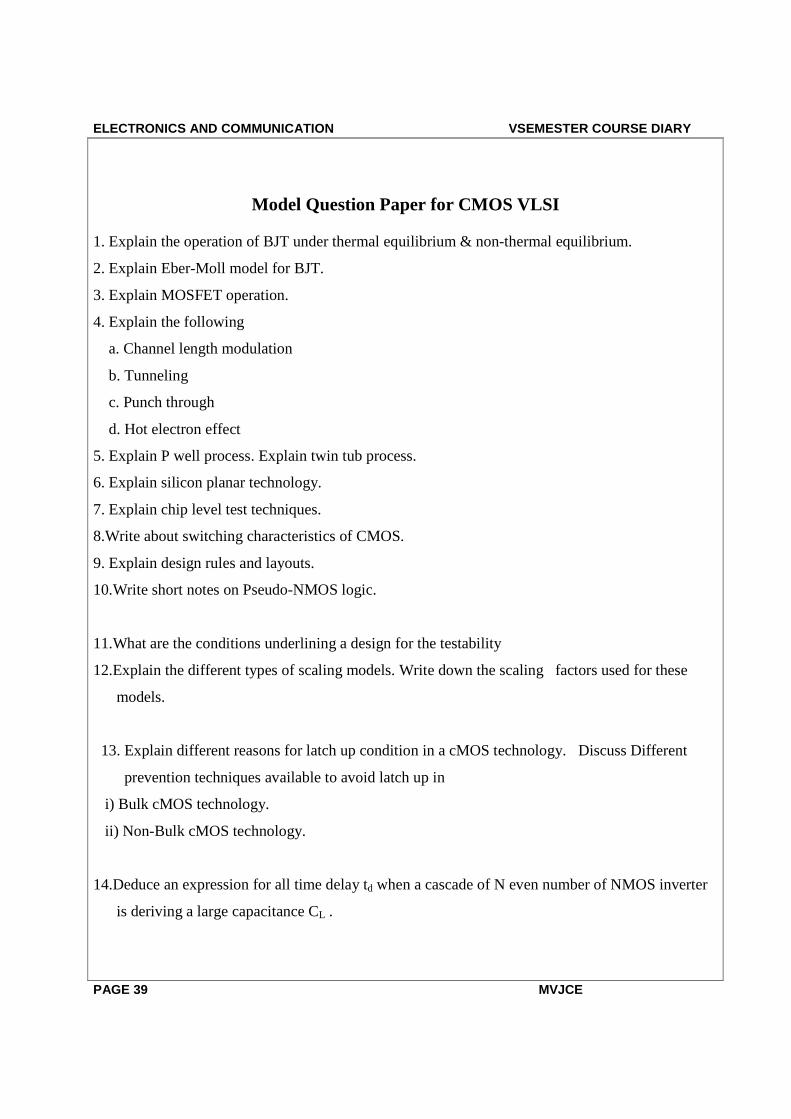
Model Question Paper for CMOS VLSI
1. Explain the operation of BJT under thermal equilibrium & non-thermal equilibrium.
2. Explain Eber-Moll model for BJT.
3. Explain MOSFET operation.
4. Explain the following
a. Channel length modulation
b. Tunneling
c. Punch through
d. Hot electron effect
5. Explain P well process. Explain twin tub process.
6. Explain silicon planar technology.
7. Explain chip level test techniques.
8.Write about switching characteristics of CMOS.
9. Explain design rules and layouts.
10.Write short notes on Pseudo-NMOS logic.
11.What are the conditions underlining a design for the testability
12.Explain the different types of scaling models. Write down the scaling factors used for these
models.
13. Explain different reasons for latch up condition in a cMOS technology. Discuss Different
prevention techniques available to avoid latch up in
i) Bulk cMOS technology.
ii) Non-Bulk cMOS technology.
14.Deduce an expression for all time delay td when a cascade of N even number of NMOS inverter
is deriving a large capacitance CL .

ELECTRONICS AND COMMUNICATION VSEMESTER COURSE DIARY
PAGE 40 MVJCE
15. Explain with neat diagram different steps involved in P-well fabrication process for CMOS
inverter.
16. Realize the following logic exprssion using CMOS structure
i) Y= (A.B.C)’
ii) Y= A(B)’+(A)’B
iii) Y= AB+ (C)’D
17. Bring out the comparison between CMOS and bipolar technologies.
18. Derive the expression for Ids for Nmos transistor starting from basics.
19. Consider the following p-channel MOSFET process:
Substrate doping Nd = 1015 cm-3 polysilicon gate doping density Nd = 1020cm-3 , gate oxide
thickness tox = 650 Å and oxide interface charge density Nox = 2* 1010 cm-2 .Use єsi =11.7e and
єox = 3.9eo for the dielectric coefficients of silicon and silicon dioxide , respectively
i) Calculate the threshold voltage Vto for Vsb =0
ii) Determine the type and the amount of the channel ion implantation which are necessary to
achieve a threshold voltage of Vto =-2v
20.With the help of a circuit digram explain invertors type NMOS super buffer

ELECTRONICS AND COMMUNICATION VSEMESTER COURSE DIARY
PAGE 41 MVJCE
06ECL-57: DIGITAL SIGNAL
PROCESSING LABORATORY

ELECTRONICS AND COMMUNICATION VSEMESTER COURSE DIARY
PAGE 42 MVJCE
SYLLABUS
Sub Code: 06ECL57 I.A. Marks: 25 Hours per week: 03 Exam Hours: 03 Total Hours: 52 Exam Marks: 50
A LIST OF EXPERIMENTS USING MATLAB/SCILAB/OCTAVE/WA B
1. Verification of Sampling theorem.
2. Impulse response of a given system
3. Linear convolution of two given sequences.
4. Circular convolution of two given sequences
5.Autocorrelation of a given sequence and verification of its properties.
6. Cross correlation of given sequences and verification of its properties.
7. Solving a given difference equation.
8. Computation of N point DFT of a given sequence and to plot magnitude and phase spectrum.
9. Linear convolution of two sequences using DFT and IDFT.
10. Circular convolution of two given sequences using DFT and IDFT
11. Design and implementation of FIR filter to meet given specifications.
12. Design and implementation of IIR filter to meet given specifications.
B. LIST OF EXPERIMENTS USING DSP PROCESSOR
1.Linear convolution of two given sequences.
2.Circular convolution of two given sequences.
3.Computation of N- Point DFT of a given sequence
4.Realization of an FIR filter ( any type ) to meet given specifications .The input can be a signal
from function generator / speech signal .
5.Audio applications such as to plot a time and frequency display of Microphone plus a cosine using
DSP. Read a wav file and match with their respective spectrograms
6.Noise removal: Add noise above 3kHz and then remove ; Interference suppression using 400 Hz
7.Impulse response of first order and second order system
References: 1.Sanjeet Mitra, Digital signal processing using MATLAB, TMH, 2001
2.J.G.Proakis & Ingale, Digital signal processing using MATLAB,.MGH, 2000
3.B.Venkataramani and Bhaskar, Digital signal processors, TMH,2002

ELECTRONICS AND COMMUNICATION VSEMESTER COURSE DIARY
PAGE 43 MVJCE
.
06ECL-58: Analog Communication Lab +
LIC Lab

ELECTRONICS AND COMMUNICATION VSEMESTER COURSE DIARY
PAGE 44 MVJCE
EXPERIMENTS
1. Second order active LPF and HPF
2. Second order active BPF and BE
3. Operational amplifier applications
i) Inverting amplifier and Non inverting amplifier
i) Inverting and non inverting adder
ii) Voltage follower, Differentiator and integrator
4. Schmitt Trigger Design and test a Schmitt trigger circuit for the given values of UTP and LTP
5. Frequency synthesis using PLL.
6. Design and test R-2R DAC using op-amp
7. Design and test the following circuits using IC 555
a. Astable multivibrator for given frequency and duty cycle
b. Monostable multivibrator for given pulse width W
8. Amplitude modulation using transistor/FET (Generation and detection) Pulse amplitude
modulation and detection
9. PWM and PPM
10. Frequency modulation using 8038/2206
11. Precision rectifiers
Suggested Reference:
1. Wayne Tomasi, Electronic Communication System, 5th Edn. 2007 PHI/Pearson Edn.

ELECTRONICS AND COMMUNICATION VSEMESTER COURSE DIARY
PAGE 45 MVJCE