Embed Size (px)
Citation preview

1
Low Insertion Loss Substrate Integrated Waveguide Quasi–Elliptic Filters for V-
Band Wireless Personal Area Network Applications.
D. Zelenchuk, V. Fusco.
Abstract: Novel high performance V-band substrate integrated waveguide (SIW)
filters have been presented in the paper. Design procedures for the filters synthesis
and mechanisms providing quasi-elliptic response have been explained. The
insertion loss of the filters has been measured below 2 dB with microstrip-to-SIW
transitions are included.
1 Introduction
Nowadays millimetre-wave systems are used well beyond their traditional niche of
military and space and have already penetrated consumer-oriented market through
applications such as automotive radars and high-speed wireless networks. Among
those applications special attention is attached to 60 GHz wireless networks. This
is stimulated by the existence of up to 9 GHz unlicensed spectrum bandwidth
between 57 and 66 GHz, [1][1]. New systems exploiting this spectrum allocation
will respond to growing demand for short-range transmission of uncompressed
high-definition audio and video content in real time with data rates of up to
3 Gbyte/sec as required for Wireless HD [2][2].
Integrated filters are an important part of such a system. However, it is difficult to
achieve low insertion loss for a filter designed at these frequencies; additionally a
printed circuit board (PCB) compliant solution strategy would be useful for cost

2
minimization for of consumer applications. At V-band CMOS microstrip filters
exhibit relatively high insertion loss (more than 4 dB) [3][3] and can be affected by
electromagnetic interference. As a PCB alternative substrate integrated waveguide
(SIW) technology has recently been proposed. A number of different devices have
been implemented which demonstrate useful good performance characteristics [4–
6]. A comprehensive review of state-of-the-art in SIW research is given in [7][7],.
Furthermore several V-band components have been designed with while SIW
technology [8–10] has begun to be applied in V-band components [8-10].
An SIW filter demonstrated in [9][10] at 62 GHz which had 3 dB insertion loss at
61-63 GHz and 15 dB return loss as well as out-of-band rejection of 25 dB and
15 dB for lower and upper stopbands respectively, . compared Ato the insertion
loss of a multilayer SIW LTCC filter reported in [10][8] with insertion loss of
around 2dB and return loss of 16 dB at 57-64 GHz as well as out-of-band rejection
of 33 dB and 25 dB for lower and upper stopbands at 3 GHz outside the passband.
In [10][8] however in order to achieve 2 dB insertion loss an additional
compensation circuit was implemented.
In this paper we propose two different low-loss SIW filter topologies with quasi-
elliptic characteristics manufactured on PTFE-based PCB substrate
TaclamPLUS [11]. The substrate offers lower loss tangent alternative to LCP and
LTCC at V-band and is suitable for mm-wave packaging. The main objective of
the paper is to demonstrate simple V-band filter designs compliant with typical
PCB process for a softboard. The design of the filters will beis discussed in the
Section 2. Then in Section 3 the measurement and the de-embedding procedures

3
will beare detailed. Results will beare discussed in Section 4 and the summary
given in the Conclusions.
4
2 Design
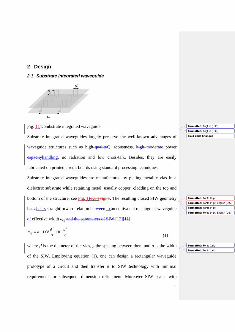
2.1 Substrate integrated waveguide
Fig. 111. Substrate integrated waveguide.
Substrate integrated waveguides largely preserve the well-known advantages of
waveguide structures such as high-qualityQ, robustness, high moderate power
capacityhandling, no radiation and low cross-talk. Besides, they are easily
fabricated on printed circuit boards using standard processing techniques.
Substrate integrated waveguides are manufactured by plating metallic vias in a
dielectric substrate while retaining metal, usually copper, cladding on the top and
bottom of the structure, see Fig. 1Fig. 1Fig. 1. The resulting closed SIW geometry
has abears straightforward relation between to an equivalent rectangular waveguide
of effective width aeff and the parameters of SIW [12][11]:
a
d
s
daaeff
22
1.008.1 (1)
where d is the diameter of the vias, s the spacing between them and a is the width
of the SIW. Employing equation (1), one can design a rectangular waveguide
prototype of a circuit and then transfer it to SIW technology with minimal
requirement for subsequent dimension refinement. Moreover SIW scales with
Formatted: English (U.K.)
Field Code Changed
Formatted: English (U.K.)
Formatted: Font: 14 pt
Formatted: Font: 14 pt, English (U.S.)
Formatted: Font: 14 pt
Formatted: Font: 14 pt, English (U.S.)
Formatted: Font: Italic
Formatted: Font: Italic

5
frequency with respect to the relative permittivity of the substrate r as r
1 , i.e.
exactly as does a homogeneously filled rectangular waveguide.
The filters presented in the paper are designed at 0.200 mm Taconic TacLamPLUS
substrate, [11][12], with permittivity of 2.1 and loss tangent of 0.0008 specified at
50 GHz. This material is specifically developed for microwave packaging purposes
as it permits ablation for creation of cavities into which MMIC chips can be
embedded, thus permitting enabling implementation of System-on-Substrate
implementation.
For the SIW filters developed in this paper the diameter of all of the vias used has
been set to 0.25 mm and their spacing chosen as 0.4 mm. This agrees well with
condition d/s<>0.5 ensuring that radiation loss is negligible [13][13]. Top
metallisation of the substrate is 17-microns thick copper, and bottom metallisation
is 1 mm thick copper. The bottom metallisation is kept intact in the etching
process.
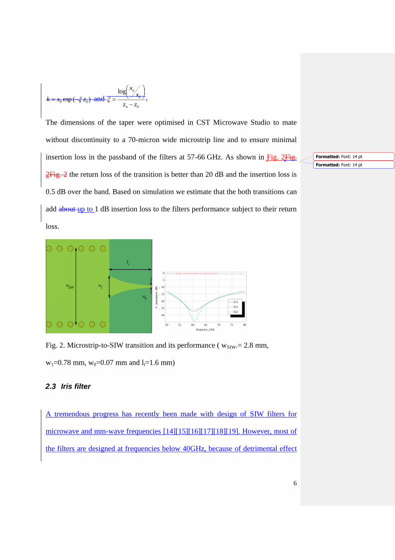
2.2 Microstrip-to-SIW transition.
There is no standard measurement interface available for a standalone SIW
structure and in order to measure them one needs to employ transitions to either
coplanar waveguide (CPW) or microstrip line. The exponential microstrip-to-SIW
transition reported in [5][5] was chosen in this work. The taper profile is given by
)(exp)( zkzx
From the two end points of the taper (x0,z0) and (xn,zn) the curve parameters are
calculated as
6
)(exp 00 zxk and 0
0
log
zz
xx
n
n
.
The dimensions of the taper were optimised in CST Microwave Studio to mate
without discontinuity to a 70-micron wide microstrip line and to ensure minimal
insertion loss in the passband of the filters at 57-66 GHz. As shown in Fig. 2Fig.
2Fig. 2 the return loss of the transition is better than 20 dB and the insertion loss is
0.5 dB over the band. Based on simulation we estimate that the both transitions can
add about up to 1 dB insertion loss to the filters performance subject to their return
loss.
50 55 60 65 70 75 80
30
25
20
15
10
5
0
frequency GHz
Spar
amet
ers
dB
S22
S21
S11
Fig. 2. Microstrip-to-SIW transition and its performance ( wSIW.= 2.8 mm,
w1=0.78 mm, w0=0.07 mm and lt=1.6 mm)
2.3 Iris filter
A tremendous progress has recently been made with design of SIW filters for
microwave and mm-wave frequencies [14][15][16][17][18][19]. However, most of
the filters are designed at frequencies below 40GHz, because of detrimental effect
Formatted: Font: 14 pt
Formatted: Font: 14 pt
7
of manufacturing tolerances. Therefore in the paper we employ simple filter
topologies which in our view are more robust with respect to manufacturing.
The first design presented here is a directly coupled resonator filter with inductive
irises employed as coupling elements. Similar filters with single and double posts
have been implemented in [5], [19]. Below, the designs are significantly advanced
in order to implement higher roll-off rate and more extended filter stopband
responses than previously reported.
For a bandpass filter with the resonators cascaded via K-inverters, normalised
impedances of the inverters are given as follows [19][14]:
100
1,0
2 ggZ
K
10
1,
2
jj
ii
ggZ
K
(2)
10
1,
2
nn
nn
ggZ
K
where Z0 is the waveguide impedance and is fractional bandwidth defined
through guided wavelength at the edges g2 and the centre of the band g0 as
0
21
g
gg
The lowpass prototype filter parameters g corresponding particular transfer
function can be found in [20][15].
Once the normalised impedances of the inverters have been found the physical
dimensions of corresponding inductive irises have to be obtained. For this
procedure we introduce use the following method [19].

8
Each iris presents itself as a K-inverter, corresponding to the reactance X, see Fig.
3Fig. 3Fig. 3.
Fig. 333. Model of inductive window in an SIW.
The parameters of the inverter are found from S-matrix of the element as:
2
21
2
11
21
0 )1(
2
SS
S
Z
Xj
0
1 2tan
Z
X
(3)
2tan
0
Z
K
Once the inverter parameters are found, the distance between adjacent inductive
windows can be evaluated as:
2
0gi
il (4)
1
2
1 iii
Following this synthesis procedure an SIW bandpass Chebyshev filter with
inductive irises can be designed.
In this paper we use the procedure to design a three pole Chebyshev filter with
0.1 dB insertion loss and 15 dB return loss in 57.36-65.76 GHz passband. First the
inverter values K are have been calculated using (2) as K01=K34=0.53 and
K12=K23=0.31. Then dependencies of K and on width of the iris window in the
Formatted: English (U.K.)
Formatted: English (U.K.)
Formatted: English (U.K.)
Field Code Changed
Formatted: English (U.K.)
Formatted: Subscript
Formatted: Subscript
Formatted: Font: Symbol

9
SIW waveguide of width a=2.8mm the widths of the iris windows corresponding
to the values are iteratively fittedhave been computed by full-wave simulations of
irises in Ansoft HFSS and then employing (3), see and Fig. 4Fig. 4. The width values
corresponding to the calculated K-values were found as w1=1.82mm and
w2=1.5mm. Substituting the phase corresponding to the widths into (4) further
analysis using (3)gives the distances between the irises as l1=l3=1.7 and l2=1.57.
These values have been taken as a first approximation and then tuned in order to
minimise the return lossAfter that the distances between the windows are found
using (4). in the passband.
1.1 1.2 1.3 1.4 1.5 1.6 1.7 1.8 1.90.0
0.2
0.4
0.6
0.8
1.0
iris width mm
K
Fig. 4. Normalised inverter impedance and phase versus iris width.
The resulting physical layout for the filter together with its S-parameters
simulated in CST Microwave StudioAnsoft HFSS is shown in Fig. 5Fig. 5Fig. 4. The
dimensions of the filter are l1=l3=1.65 mm, l2=1.6mm, a=2.8mm, w1=1.76 and
w2=1.47. The insertion loss is less than 1 1 dB. The rejection roll-off properties of
the filter at higher frequencies are relatively poor.
Formatted: Font: Italic
Formatted: Subscript
Formatted: Subscript
Formatted: Subscript
Formatted: Subscript
Formatted: Subscript
Formatted:MathematicaFormatStandardForm
Formatted: English (U.K.)
Formatted: English (U.K.)
Formatted: English (U.K.)

10
50 55 60 65 70 75 8035
30
25
20
15
10
5
0
frequency GHzS
par
amet
ers
dB
S11
S21
Fig. 554. Bandpass substrate integrated waveguide filter.
In order to improve the stopband response an additional stub action producing as
a filter transmission zero is introduced into the design, see Fig. 6Fig. 6Fig. 5. The
dimensions of the stub as optimised by numerical simulations are ws=2.8 mm and
ls=5.4 mm.
50 55 60 65 70 75 80
0
0.5
1
2
frequency GHz
K
50 55 60 65 70 75 8035
30
25
20
15
10
5
0
frequency GHz
S21
dB
Fig. 665. SIW stub and its performance normalised inverter impedance and phase
for ws=2.8 mm and ls=5.4 mm.
The stub is itself a highly-dispersive inverter which has transmission zeros. Such
inverters can be incorporated into a synthesis procedure for direct-coupled
Formatted: English (U.K.)
Field Code Changed
Formatted: English (U.K.)
Formatted: Font: 14 pt
Formatted: Font: 14 pt, English (U.S.),Check spelling and grammar
Formatted: Font: 14 pt
Formatted: Font: 14 pt, English (U.S.),Check spelling and grammar
Formatted:MathematicaFormatStandardForm
Formatted: English (U.K.)
Field Code Changed
Formatted: English (U.K.)
Formatted: English (U.K.)
Formatted: English (U.K.)
Formatted: English (U.K.)
Formatted: Font: 14 pt
Formatted: text, Line spacing: Double
Formatted: Font: 14 pt

11
resonator filters, as the one presented above [21]. There is a simpler alternative
approach which is to synthesize an inverter with impedance equal to 1 in the
passband and transmission zeros in the stopband. Such a stub can be added to an
existing filter to improve its stopband performance. With this approach in mind a
stub dimensions were optimised by numerical simulations as ws=2.8 mm and
ls=5.4 mm.
As shown in Fig. 6Fig. 6Fig. 5 the stub introduces three transmission zeros at 50,
68 and 79 GHz and about 0.1 dB insertion losses in the centre of the passband and
0.5 at the edgesits normalised impedance exceeds 0.85 in the passband and phase
close to -/2. Therefore upon properly adjusting the length of the connecting
waveguide section one can combine the iris filter with the stub section in order to
improve the stopband response of the filter while almost not compromising its
passband performance. It has to be noted that in contrast to technique proposed in
the transfer function of the filter is not Chebyshev anymore[16] the stub is
synthesised separately from the passband filter. The length of the connecting
section was accordingly adjusted to lo=1.1mm. The resultant filter with microstrip-
to-SIW transitions attached and its S-parameters in simulated in Ansoft HFSS are
shown in Fig. 7Fig. 7Fig. 6.
The filter has a sharp roll-off and wide stopband covering the 68-80 GHz range
with out-of-band rejection better than 10dB and transmission zeros at 68GHz and
80GHz. Despite overall improvement, rejection at 78GHz has risen from 12dB to
10dB which is due to a mismatch caused by the stub. The composite insertion loss
is less than 1.7 dB within in the passband. The increase in the insertion loss is
Formatted: Font: Not Italic
Formatted: Font: Not Italic
Formatted: Font: 14 pt
Formatted: Font: 14 pt, English (U.K.)
Formatted: Font: 14 pt, Check spellingand grammar
Formatted: Font: 14 pt, English (U.K.)
Formatted: Font: 14 pt, Check spellingand grammar
Formatted: Font: Symbol
Formatted: English (U.K.)
Formatted: English (U.K.)

12
attributed to the microstrip-to-SIW transitions, which contribute around 1 dB, as
discussed earlier.
50 55 60 65 70 75 8050
40
30
20
10
0
frequency GHz
Spar
amet
ers
dB
S22
S21
S11
50 55 60 65 70 75 8050
40
30
20
10
0
frequency GHz
Spa
ram
eter
sdB
S22
S21
S11
Fig. 776. Bandpass filter with enhanced stopband and microstrip launch ports,
lo=1.1 mm.
2.4 Cavity filter.
The second design suggested in the paper is a filter with an over-moded cavity, see
Fig. 8Fig. 8Fig. 7. The design of the filter is based on the multi-mode cavity filters
techniques reported in [22–24][17,18]. A rigorous design procedure that prescribes
the positions of the poles and transmission zeros through a coupling matrix
synthesis for multi-mode cavities is presented in [23][18]. However, the approach
requires substantial full-wave simulation in order to synthesise appropriate inter-
cavities mode couplings as well as source and load coupling to the modes. The
procedure involves multi-parametric tuning, which for small number of cavities is
straightforward if the optimisation technique proposed in [22][17] is followed, with
Formatted:MathematicaFormatStandardForm
Formatted: English (U.K.)
Field Code Changed
Formatted: English (U.K.)
Formatted: English (U.K.)
Formatted: English (U.K.)
Formatted: English (U.K.)

13
the additional constraint that in this paper we enforce realistic technology
restrictions that will be encountered at the fabrication stage.
At the initial design stage the preliminary dimensions of the cavities are were
chosen and subsequently the entire structure is optimised in order to provide the
required spectral response, taking into account the equivalence of a SIW and a
rectangular waveguide. The equivalent structure was optimised in the Microwave
Wizard waveguide simulator, [25], with the aim of ensuring 0.1dB insertion loss
and 15dB return loss in the same passband as previous filter. The first
approximation for the cavity dimensions were taken as w3=w6=6.9mm and
l2=l3=1.85mm in order to ensure that both TE101 and TE102 modes are resonant in
the passband. The position and dimensions of the coupling irises are optimised that
the transmission zeros appear both in the lower and the upper stopband due to the
negative coupling between the modes. In order to reduce the sensitivity of the filter
response to the PCB manufacturing process several topology restrictions were
enforced. First the inter-cavity wall has been implemented with single row of vias
of exactly the same diameter as all other vias in the design. Second, the iris in the
wall is located at the side of the wall, this reduces the number of objects in this
sensitive area. Finally, input and output irises are of the same dimensions as the
corresponding SIW waveguide sections. The equivalent structure was optimised in
the Microwave Wizard waveguide simulator, [19], with the aim of ensuring low
insertion loss passband between 57 - 66 GHz and stop bands outside of this range.
Then, with the aid of (1) the design was transferred to SIW PCB and simulated in
CST Microwave Studio.
Formatted: Subscript
Formatted: Subscript
Formatted: Subscript
Formatted: Subscript
Formatted: Subscript
Formatted: Subscript

14
In order to reduce the sensitivity of the filter response to the PCB manufacturing
process several topology restrictions were enforced. First the inter-cavity wall has
been implemented with single row of vias of exactly the same diameter as all other
vias in the design. Second, the iris in the wall is located at the side of the wall, this
reduces the number of objects in this sensitive area. Finally, input and output irises
are of the same dimensions as the corresponding SIW waveguide sections.
As a result the dimensions of the filter were set as follows: w1=2.55 mm,
w2=1.56mm, w3=6.32 mm, w4=1.71 mm, w5=2.11 mm, w6=6.71 mm,
w7=2.25 mm, l1=1.84 mm, l2=1.84 mm, l3=1.65 mm, l4=2.5 mm, and l5=1.12 mm.
The response of the filter is presented in Fig. 8Fig. 8Fig. 7. The insertion loss
including launch transitions is better than 1.7 dB in the 57-66 GHz passband and
the stopbands measured at -10dB level cover 52-55GHz and 68-75GHz bands. The
latter has been achieved due to placement of transmission zeros at 53, 70 and
74GHz in the optimisation goal function.
The transmission zeros in the stopband are the consequence of the destructive
interference between different modes coexisting in the filter cavities at the ports
and/or cavity interfaces. For example, the study of the field distribution reveals that
there are three resonant modes in the larger cavity within the passband. However
extraction of the detailed equivalent topology is beyond the scope of the paper, but
could be considered in future work following the methods proposed in [23][18].
The spurious transmission bands in near 50GHz and 75GHz are not of concern in
this paper since the filter is designed to be part of an integrated front-end where
active components will not be operating at the frequencies. Yet, the authors realise
Formatted: Font: 14 pt
Formatted: Font: 14 pt, English (U.S.),Check spelling and grammar
Formatted: Font: 14 pt
Formatted: Font: 14 pt, English (U.S.),Check spelling and grammar

15
it can be of concern for some application and will attempt to improve it in the
future work.
50 55 60 65 70 75 8040
30
20
10
0
frequency GHz
Spar
amet
ers
dB
S22
S21
S11
Fig. 887. Cavity filter design and simulated performance.
3 Measurement
3.1 Measurement setup
The structures were measured using a Cascade millimetre-wave probe station with
50 ohm ground-signal-ground (GSG) probes. The pitch of the probes is 150
microns. The probes before each measurement were calibrated using an automated
LLRM-procedure at the probe station and the calibration error was below 0.1 dB
for the entire frequency range from 50 to 80 GHz.
3.2 De-embedding
In order to the interface to GSG probes, the circuits were terminated at the coplanar
waveguide with ground plane (CPWG) probe pads, see Fig. 9Fig. 9Fig. 8. The
dimensions of the pads were chosen to comply with PCB etching process
restriction of 70 microns on the smallest feature dimension and the 150 micron
pitch of the 50 Ohm GSG probe. The microstrip line width in the transition is
Formatted: English (U.K.)
Field Code Changed
Formatted: English (U.K.)
Formatted: English (U.K.)
Formatted: Font: 14 pt
Formatted: Font: 14 pt

16
70 microns, the gap width is 80 microns, the diameter of via is 250 microns and the
area of each pad is 1mmx0.45mm.
The chosen dimensions do not ensure good matching to the probe since neither
CPWG nor microstrip line impedance is 50 Ohm, indeed for the dimensions used
they are 100 and 135 Ohms, correspondingly. Hence a robust de-embedding
procedure has to be applied in order to exclude the effect that these pads have on
measurement results.
Fig. 998. CPWG-microstrip transition and transmission line calibration set.
In order to de-embed the CPWG-microstrip transitions an adaption of the method
reported in [26][20] is has next been employed. The method is based on extracting
the ABCD-matrix of the transition by measuring two uniform transmission lines of
different length terminated with transitions.
Two microstrip lines 6mm and 7mm long terminated with transitions have been
fabricated and measured, see Fig. 9Fig. 9Fig. 8. Each of the calibration samples is
described by ABCD-matrix as follows [26][20]:
)cos()sin(
)sin()cos(1
0
0
llZ
lZl
DC
BA
cal
where is the complex propagation constant, l is the length of the uniform
transmission line and
is the ABCD-matrix of the CPWG-microstrip
transition. Following the approach given in [26][20], the ABCD-matrices of the
Formatted: Font: 14 pt
Formatted: Font: 14 pt

17
transitions have been found. Unfortunately the analytical LC-circuit derived from
the ABCD-matrix in [16] fails to account for the loss in the pads and consequently
the ABCD-matrices of the transitions themselves are used.
The measured transmission matrix of the device under test (DUT) with the
transitions reads as
DUTpadsDUTDC
BA
DC
BA
The de-embedded transmission matrix of the DUT can then be found as
11
padsDUTDUTDC
BA
DC
BA
In order to illustrate the effect of the procedure the S-parameters of the 6mm
transmission line with pads and de-embedded are presented in Fig. 10Fig. 10Fig. 9.
50 55 60 65 70 75 8025
20
15
10
5
0
frequency GHz
Spar
amet
ers
dB
S22
S21
S11
With pads
50 55 60 65 70 75 8025
20
15
10
5
0
frequency GHz
Spar
amet
ers
dB
S22S21S11
With pads
50 55 60 65 70 75 8050
40
30
20
10
0
frequency GHz
Spar
amet
ers
dB
S22
S21
S11
De embedded
50 55 60 65 70 75 8050
40
30
20
10
0
frequency GHz
Spar
amet
ers
dB
S22S21S11
Fig. 10109. S-parameters of 6mm long microstrip line: before and after de-
embedding.
Formatted: Font: 14 pt
Formatted: Font: 14 pt
Formatted: English (U.K.)
Formatted:MathematicaFormatStandardForm
Formatted: English (U.K.)
Formatted:MathematicaFormatStandardForm

18
As one can see from Fig. 10Fig. 10Fig. 9 the return loss is better than 20 30 dB
across the frequency range, confirming that the DUT is a well-matched
transmission line. The difference between S11 and S22 in both plots might be
attributed to the probe positioning uncertainty and manufacturing tolerances.
The same factors contribute to numerical errors of the de-embedding resulting in
Tthe kinks of insertion loss in the range between 61 and 65 GHz seem to be an
artifact persistently manifested for all measured calibration samples. The effect is
too big to be a measurement calibration error, which was known to be below
0.1 dB across the band. Most probably this is due to a combination of measurement
uncertainties and Our studies have shown that the effect can be reduced if one to
enforce the S-matrix symmetry of the calibration samples.numerical error of de-
embedding. Unfortunately, both calibration samples satisfy resonant conditions at
the frequency range, which enhances the numerical error. One also has to
remember that the method implies identity of all the transitions which is not true
due to the manufacturing tolerances. Thus the de-embedding error can accumulate
at particular frequencies and cancel out at the others. Since the SIW structures are
shielded there is no apparent physical mechanism which can produce those kinks
within the filters. This artefact error influences all the de-embedded results
presented below. Therefore when the insertion loss is estimated the artefact is
discarded.
Formatted: Font: 14 pt
Formatted: Font: 14 pt

19
4 Results
Fig. 111110. Manufactured filters.
The manufactured filters are presented in Fig. 11Fig. 11Fig. 10. The filters were
measured and the results were de-embedded according to the method described
above. As shown in Fig. 12Fig. 12Fig. 11 the responses of both filters are shifted
towards lower than predicted frequencies when compared with results simulated
for the substrate with permittivity of 2.1. In fact both manufacturing and
permittivity tolerances can contribute to the shift of passband; below we have
attempted to correct the latter as it is major factor in our view. Bearing in mind
scaling properties of SIW with respect to permittivity discussed in Section 2 the
actual material permittivity was estimated to be 2.06 by fitting the positions of
transmission zeros in the responses. Simulations with this value of permittivity
were performed and the results were compared with the experimental ones in Fig.
13Fig. 13Fig. 12. For both filters the experimental results are in a very good
agreement with the simulations for the adjusted value of the permittivity.
In view of the explanation of the insertion loss kinks in the passband given in
Section 3 one can conclude that the overall insertion loss in the passband is better
Formatted: Font: 14 pt
Formatted: Font: 14 pt
Formatted: Font: 14 pt
Formatted: Font: 14 pt
Formatted: Font: 14 pt
Formatted: Font: 14 pt

20
than 2dB for both filters. Additionally, around 1dB is contributed by the
microstrip-to-SIW transitions, which means that the SIW filters introduce less than
1 dB insertion loss.
50 55 60 65 70 75 8050
40
30
20
10
0
frequency GHz
Spar
amet
ers
dB
S21 simulated
S21 measured
S11 simulated
S11 measured
Cavity filter r 2.1
50 55 60 65 70 75 8050
40
30
20
10
0
frequency GHz
Spa
ram
eter
sdB
S21 simulated
S21 measured
S11 simulated
S11 measured
Cavity filter r 2.1
50 55 60 65 70 75 8040
30
20
10
0
frequency GHz
Spar
amet
ers
dB
S21 simulated
S21 measured
S11 simulated
S11 measured
Cavity filter r 2.1
50 55 60 65 70 75 8050
40
30
20
10
0
frequency GHz
Spa
ram
eter
sdB
S21 simulated
S21 measured
S11 simulated
S11 measured
Cavity filter r 2.1
Fig. 121211. Comparison of measured and simulated performance for the iris filter
and the cavity filter with permittivity of 2.1.
Formatted: English (U.K.)
Formatted:MathematicaFormatStandardForm
Formatted: English (U.S.)
Formatted: English (U.K.)
Formatted:MathematicaFormatStandardForm

21
50 55 60 65 70 75 8050
40
30
20
10
0
frequency GHz
Spar
amet
ers
dB
S21 simulated
S21 measured
S11 simulated
S11 measured
Cavity filter r 2.06
50 55 60 65 70 75 8050
40
30
20
10
0
frequency GHz
Spa
ram
eter
sdB
S21 simulated
S21 measured
S11 simulated
S11 measured
Cavity filter r 2.06
50 55 60 65 70 75 8040
30
20
10
0
frequency GHz
Spar
amet
ers
dB
S21 simulated
S21 measured
S11 simulated
S11 measured
Cavity filter r 2.06
50 55 60 65 70 75 8050
40
30
20
10
0
frequency GHz
Spa
ram
eter
sdB
S21 simulated
S21 measured
S11 simulated
S11 measured
Cavity filter r 2.06
Fig. 131312. Comparison of measured and simulated performance for the iris filter
and the cavity filter with permittivity of 2.06.
5 Conclusions
Two novel high performance V-band filters with quasi-elliptic responses have been
presented in the paper. Design procedures for the filters synthesis, physical
mechanisms providing quasi-elliptic response and de-embedding of the measured
results have been explained. The insertion loss of the filters is measured below
2 dB when microstrip-to-SIW transitions are included. The return loss in passband
is measured below 10dB, which is to be improved in future work. The filters have
sharp roll-off due to the transmission zeros and the out-of-band rejection in the
upper stopband of 10dB and 17dB. It has been estimated that the SIW filters
themselves introduce less than 1 dB insertion loss. Both filters can be used as an
advanced packaging solution for V-band wireless personal network front-end
applications.
Formatted: English (U.K.)
Formatted:MathematicaFormatStandardForm
Formatted: English (U.S.)
Formatted: English (U.K.)
Formatted:MathematicaFormatStandardForm

22
6 Acknowledgements
This work was supported by the Engineering and Physical Sciences Research
Council (U.K.) under EPSRC Grant EP/E01707X/1 and by Northern Ireland
Department for Employment and Learning under “Strengthening All Island—
“Mobile Wireless Futures” research program. Authors wish to thank Taconic
International Ltd., Mullingar, Ireland for support and provided materials, and
Varioprint AG, Heiden, Switzerland for fabrication of the circuits. Authors also
wish to acknowledge stimulating discussions and advice provided by Dr George
Goussetis.
7 References
[1] “http://www.ecma-international.org/publications/files/ECMA-ST/ECMA-
387.pdf.”
[2] “http://www.wirelesshd.org/.”
[3] C.-H. Liu, C.-Y. Hsu, C.-Y. Chen, and H.-R. Chuang, “60-GHz bandpass
filter with ACMRC resonator fabricated using 0.18-mum CMOS
technology,” Microwave and Optical Technology Letters, vol. 51, 2009, pp.
597-600.
[4] C. Zhong, J. Xu, Z. Yu, and J. Li, “Miniaturized antenna using half-mode
substrate integrated waveguide structure,” Microwave and Optical
Technology Letters, vol. 50, Dec. 2008, pp. 3214-3218.
[5] Z. Sotoodeh and B. Biglarbegian, “A novel bandpass waveguide filter
structure on SIW technology,” Progress In Electromagnetics Research
Letters, vol. 2, 2008, pp. 141-148.

23
[6] F. Xu and K. Wu, “Periodic Leaky-Wave Antenna for Millimeter Wave
Applications Based on Substrate Integrated Waveguide,” Antennas and Propagation, IEEE Transactions on, vol. 58, 2010, pp. 340-347.
[7] M. Bozzi, L. Perregrini, K. Wu, and P. Arcioni, “Current and Future
Research Trends in Substrate Integrated Waveguide Technology,”
Radioengineering, vol. 18, 2009, pp. 201-209.
[8] G. Lee, C. Yoo, Y. Kim, J. Kim, Y. Park, and J. Yook, “A 60 GHz
Embedded SIW (Substrate Integrated Waveguide) BPF Considering the
Transition Effect,” IEEE Asia Pacific Microwave Conference, Singapore:
2009, pp. 1192-1195.
[9] Q. Lai, C. Fumeaux, W. Hong, and R. Vahldieck, “60 GHz Aperture-
Coupled Dielectric Resonator Antennas Fed by a Half-Mode Substrate
Integrated Waveguide,” Antennas and Propagation, IEEE Transactions on,
vol. 58, 2010, pp. 1856-1864.
[10] K. Tokuda, “A V-band planar narrow bandpass filter using a new type
integrated waveguide transition,” IEEE Microwave and Wireless
Components Letters, vol. 14, Dec. 2004, pp. 545-547.
[11] F. Xu and K. Wu, “Guided-wave and leakage characteristics of substrate
integrated waveguide,” IEEE Transactions on Microwave Theory and
Techniques, vol. 53, Jan. 2005, pp. 66-73.
[12] “http://www.taconic-add.com/pdf/taclamplus.pdf.”
[13] M. Bozzi and L. Perregrini, “Modeling of Conductor, Dielectric, and
Radiation Losses in Substrate Integrated Waveguide by the Boundary
Integral-Resonant Mode Expansion Method,” IEEE Transactions on
Microwave Theory and Techniques, vol. 56, Dec. 2008, pp. 3153-3161.
[14] D. Deslandes and K. Wu, “Millimeter-wave substrate integrated waveguide
filters,” IEEE CCECE Canadian Conference on Electrical and Computer
Engineering, Montreal: 2003, pp. 1917-1920.
[15] J. Hong and M. Lancaster, Microstrip filters for RF/microwave applications,
New York: John Wiley & Sons, Inc., 2001.
[16] S. Amari and J. Bornemann, “Using frequency-dependent coupling to
generate finite attenuation poles in direct-coupled resonator bandpass filters,”
IEEE Microwave and Guided Wave Letters, vol. 9, 1999, pp. 404-406.

24
[17] M. Guglielmi, P. Jarry, E. Kerherve, O. Roquebrun, and D. Schmitt, “A new
family of all-inductive dual-mode filters,” IEEE Transactions on Microwave Theory and Techniques, vol. 49, 2001, p. 1764–1769.
[18] U. Rosenberg and S. Amari, “Novel design possibilities for dual-mode filters
without intracavity couplings,” IEEE Microwave and Wireless Components
Letters, vol. 12, Aug. 2002, pp. 296-298.
[19] “Mician Microwave Wizard,
http://www.mician.com/cms/content/products/wave_wizard.”
[20] R. Torres-Torres, G. Hernandez-Sosa, G. Romo, and A. Sanchez,
“Characterization of Electrical Transitions Using Transmission Line
Measurements,” IEEE Transactions on Advanced Packaging, vol. 32, Feb.
2009, pp. 45-52.
[1] “High Rate 60 GHz PHY, MAC and HDMI PAL, Standard ECMA-387, Ecma
International, Dec. 2010 [Online]. Available: http://www.ecma-
international.org/publications/files/ECMA-ST/ECMA-387.pdf.” .
[2] “http://www.wirelesshd.org/.” .
[3] C.-H. Liu, C.-Y. Hsu, C.-Y. Chen, and H.-R. Chuang, “60-GHz bandpass filter with
ACMRC resonator fabricated using 0.18-mum CMOS technology,” Microwave and
Optical Technology Letters, vol. 51, no. 3, pp. 597-600, 2009.
[4] C. Zhong, J. Xu, Z. Yu, and J. Li, “Miniaturized antenna using half-mode substrate
integrated waveguide structure,” Microwave and Optical Technology Letters, vol. 50, no.
12, pp. 3214-3218, Dec. 2008.
[5] Z. Sotoodeh and B. Biglarbegian, “A novel bandpass waveguide filter structure on SIW
technology,” Progress In Electromagnetics Research Letters, vol. 2, pp. 141-148, 2008.
[6] F. Xu and K. Wu, “Periodic Leaky-Wave Antenna for Millimeter Wave Applications
Based on Substrate Integrated Waveguide,” Antennas and Propagation, IEEE
Transactions on, vol. 58, no. 2, pp. 340-347, 2010.
[7] M. Bozzi, L. Perregrini, K. Wu, and P. Arcioni, “Current and Future Research Trends in
Substrate Integrated Waveguide Technology,” Radioengineering, vol. 18, no. 2, pp. 201-
209, 2009.
[8] Q. Lai, C. Fumeaux, W. Hong, and R. Vahldieck, “60 GHz Aperture-Coupled Dielectric
Resonator Antennas Fed by a Half-Mode Substrate Integrated Waveguide,” Antennas and
Propagation, IEEE Transactions on, vol. 58, no. 6, pp. 1856-1864, 2010.
[9] K. Tokuda, “A V-band planar narrow bandpass filter using a new type integrated
waveguide transition,” IEEE Microwave and Wireless Components Letters, vol. 14, no.
12, pp. 545-547, Dec. 2004.
Formatted: English (U.S.)
25
[10] G. Lee, C. Yoo, Y. Kim, J. Kim, Y. Park, and J. Yook, “A 60 GHz Embedded SIW
(Substrate Integrated Waveguide) BPF Considering the Transition Effect,” in IEEE Asia
Pacific Microwave Conference, 2009, pp. 1192-1195.
[11] “http://www.taconic-add.com/pdf/taclamplus.pdf.” .
[12] F. Xu and K. Wu, “Guided-wave and leakage characteristics of substrate integrated
waveguide,” IEEE Transactions on Microwave Theory and Techniques, vol. 53, no. 1, pp.
66-73, Jan. 2005.
[13] M. Bozzi and L. Perregrini, “Modeling of Conductor, Dielectric, and Radiation Losses in
Substrate Integrated Waveguide by the Boundary Integral-Resonant Mode Expansion
Method,” IEEE Transactions on Microwave Theory and Techniques, vol. 56, no. 12, pp.
3153-3161, Dec. 2008.
[14] X.-P. Chen and K. Wu, “Self-equalised pseudo-elliptical filter made of substrate
integrated waveguide,” Electronics Letters, vol. 45, no. 2, pp. 112-113, 2009.
[15] C.-C. Chuang, H.-H. Lin, and C.-L. Wang, “Design of dual-mode SIW cavity filters,”
IEEE Region 10 Conference TENCON, pp. 1-4, Oct. 2007.
[16] X. Chen, W. Hong, Z. Hao, and K. Wu, “Substrate integrated waveguide quasi-elliptic
filter using extracted-pole technique,” in Asia-Pacific Conference Proceedings, 2005, vol.
1, p. 3.
[17] Q.-F. Wei, Z.-F. Li, L. Li, W.-J. Zhang, and J.-F. Mao, “Three-pole cross-coupled
substrate-integrated waveguide bandpass filters based on PCB process and multilayer
LTCC technology,” Microwave and Optical Technology Letters, vol. 51, no. 1, pp. 71-73,
2009.
[18] Y. Dong, W. Hong, H. Tang, J. Chen, and K. Wu, “Planar realization of a Q-band triple-
mode filter using high-order resonances,” Microwave and Optical Technology Letters,
vol. 51, no. 3, pp. 600-603, 2009.
[19] D. Deslandes and K. Wu, “Millimeter-wave substrate integrated waveguide filters,” in
IEEE CCECE Canadian Conference on Electrical and Computer Engineering, 2003, vol.
3, pp. 1917-1920.
[20] J. Hong and M. Lancaster, Microstrip filters for RF/microwave applications, vol. 7. New
York: John Wiley & Sons, Inc., 2001, pp. 0-471.
[21] S. Amari and J. Bornemann, “Using frequency-dependent coupling to generate finite
attenuation poles in direct-coupled resonator bandpass filters,” IEEE Microwave and
Guided Wave Letters, vol. 9, no. 10, pp. 404-406, 1999.
[22] M. Guglielmi, P. Jarry, E. Kerherve, O. Roquebrun, and D. Schmitt, “A new family of all-
inductive dual-mode filters,” IEEE Transactions on Microwave Theory and Techniques,
vol. 49, no. 10 Part 1, pp. 1764–1769, 2001.
[23] U. Rosenberg and S. Amari, “Novel design possibilities for dual-mode filters without
intracavity couplings,” IEEE Microwave and Wireless Components Letters, vol. 12, no. 8,
pp. 296-298, Aug. 2002.

26
[24] X.-P. Chen, K. Wu, and D. Drolet, “Substrate Integrated Waveguide Filter With Improved
Stopband Performance for Satellite Ground Terminal,” IEEE Transactions on Microwave
Theory and Techniques, vol. 57, no. 3, pp. 674-683, Mar. 2009.
[25] “Mician Microwave Wizard,
http://www.mician.com/cms/content/products/wave_wizard.” .
[26] R. Torres-Torres, G. Hernandez-Sosa, G. Romo, and A. Sanchez, “Characterization of
Electrical Transitions Using Transmission Line Measurements,” IEEE Transactions on
Advanced Packaging, vol. 32, no. 1, pp. 45-52, Feb. 2009.