Embed Size (px)
Citation preview
Personal Mechatronics Lab
Utility Board User Manual
©2012 by M.R. Emami

Utility Board User Manual
Personal Mechatronics Lab 1
1 Table of Contents
1 Table of Contents .................................................................................................................................. 1
2 Introduction .......................................................................................................................................... 3
2.1 Overview ....................................................................................................................................... 3
2.2 Modules ........................................................................................................................................ 4
2.2.1 Power Module ....................................................................................................................... 4
2.2.2 Transistor Tester ................................................................................................................... 4
2.2.3 IR Emitter Tester ................................................................................................................... 4
2.2.4 Continuity Tester ................................................................................................................... 4
2.2.5 Function Generator ............................................................................................................... 4
2.2.6 Battery Charger ..................................................................................................................... 5
2.2.7 Oscilloscope .......................................................................................................................... 5
3 Power Module ....................................................................................................................................... 6
3.1 Instructions ................................................................................................................................... 6
3.2 Schematic ...................................................................................................................................... 7
3.3 Power Control ............................................................................................................................... 7
3.4 Voltage Converter ......................................................................................................................... 7
3.5 Filtering ......................................................................................................................................... 8
3.6 ON/OFF Switch .............................................................................................................................. 8
4 Transistor Tester ................................................................................................................................... 9
4.1 Instructions ................................................................................................................................... 9
4.2 Schematic .................................................................................................................................... 10
4.3 Determining Functionality .......................................................................................................... 10
4.4 Pin Arrangement ......................................................................................................................... 11
4.5 Method of Testing ....................................................................................................................... 11
4.6 Female Header Arrangement ..................................................................................................... 11
5 IR Emitter Tester ................................................................................................................................. 12
5.1 Instructions ................................................................................................................................. 12
5.2 Schematic .................................................................................................................................... 12
5.3 Determining Functionality .......................................................................................................... 13

Utility Board User Manual
Personal Mechatronics Lab 2
6 Continuity Tester ................................................................................................................................. 14
6.1 Instructions ................................................................................................................................. 14
6.2 Schematic .................................................................................................................................... 15
6.3 Sound .......................................................................................................................................... 15
6.4 Connection Notes ....................................................................................................................... 15
6.5 Connection Types ........................................................................................................................ 15
7 Function Generator ............................................................................................................................. 16
7.1 Instructions ................................................................................................................................. 16
7.2 Schematic .................................................................................................................................... 17
7.3 Output Waveforms ..................................................................................................................... 18
7.4 Frequency Adjustment ................................................................................................................ 18
7.5 Potentiometers (trimmers) ......................................................................................................... 18
8 Battery Charger ................................................................................................................................... 19
8.1 Instructions ................................................................................................................................. 19
8.2 Schematic .................................................................................................................................... 21
8.3 Number of Cells........................................................................................................................... 21
8.4 Power .......................................................................................................................................... 21
8.5 Trickle/Fast Charge ..................................................................................................................... 22
8.6 Heat issues .................................................................................................................................. 22
8.7 General Information on NiMH Batteries ..................................................................................... 23
9 Oscilloscope ........................................................................................................................................ 24
9.1 Instructions ................................................................................................................................. 24
9.2 Schematic .................................................................................................................................... 25
9.3 Installation .................................................................................................................................. 26
9.4 PIC Firmware ............................................................................................................................... 26
9.5 Programming the PIC .................................................................................................................. 27
9.6 PC Driver ..................................................................................................................................... 27
9.7 PC Application ............................................................................................................................. 27
9.8 Data Acquisition .......................................................................................................................... 30
9.9 PIC Driver Mode .......................................................................................................................... 31

Utility Board User Manual
Personal Mechatronics Lab 3
Figure 1: Overview of the Utility Board and its modules
2 Introduction
2.1 Overview
Utility Board is a testing, charging, monitoring and signal generator board developed to aid
post-secondary students and designers with electronic design projects. It is powered entirely
using USB power with a built in DC-DC converter. It contains six distinct modules, some of which
are connected to each other - a transistor tester, IR emitter tester, continuity tester, a signal
generator (square, triangle and sine) capable of producing signals up to 100KHz, an oscilloscope
capable of simultaneous monitoring of dual channel analog signals up to 30 KHz, and a battery
charger that can charge up to 8 NiCd or NiMH cells at a time.

Utility Board User Manual
Personal Mechatronics Lab 4
2.2 Modules
Below is a brief description of the features and purpose of each of the modules.
2.2.1 Power Module
The power module supplies power for all modules including the battery charger. Upon
connecting the board to a USB port (PC or a wall outlet), the battery module is powered with
+12V. This allows the other modules to be turned off while charging overnight or for extended
periods of time. Upon switching on the board, the board is simultaneously supplied with 5V,
+12V and -12V to power all other modules. The +12V and -12V is attained from the USB port
using a DC-DC converter. This makes it very simple to power the board.
2.2.2 Transistor Tester
The transistor tester checks the functionality of NPN or PNP transistors of any pin configuration.
It determines in which of three states the transistor is in – (A) functional; (B) base-collector
short or collector-emitter short; or (C) base-emitter short. This tester is able to test out larger
transistor packages on board.
2.2.3 IR Emitter Tester
This module allows the user to connect an infrared emitter and determine its functionality
through an indicator LED. Alternatively, the user may position the Utility Board near an IR
emitter in an external circuit. But in either case, the detector on the Utility Board must be
within 10 mm of the emitter.
2.2.4 Continuity Tester
The continuity tester tests the connection between traces, wires, and solders points. The tester
is rated at 30Ω. Therefore, it detects resistance less than 30Ω as being a short circuit. When two
points are electrically connected, the buzzer beeps, indicating a connection. The buzzer is a
piezo electric device that produces high decibels using low current usage.
2.2.5 Function Generator
The function generator module on the Utility Board uses the XR2206 controller to produce
square, triangular, or sinusoidal waves of up to 100kHz or as low as 1Hz, with a tested range of
-10V to +10V. Using jumpers and trimmers, one can adjust offset, frequency, duty cycle, and
amplitude. One common use for a function generator is to produce a clock signal for the Driver
Board, for example.

Utility Board User Manual
Personal Mechatronics Lab 5
2.2.6 Battery Charger
This module allows the user to charge between 1 and 8 NiMH rechargeable battery cells, with a
typical charge time of 3 hours. It has fast charge and a trickle charge mode that is
autonomously controlled to allow for efficient charging.
2.2.7 Oscilloscope
This module’s primary function is a dual channel PC oscilloscope with a maximum sampling rate
of 30kHz. It contains a PIC18F2550 microcontroller, which runs as an HID USB device and
interfaces to a Windows PC.
Its secondary function is to act as a regular PIC driver. 18 input/output pins are included in the
module to allow the user to run custom code on the PIC, with the option of communicating
with a PC through the USB interface for advanced users. The mounted oscillator clock
frequency is 20 MHz. Furthermore, the PIC can be programmed using bootloader by pressing
the boot switch down while powering the board.

Utility Board User Manual
Personal Mechatronics Lab 6
Figure 2: Physical location of the Power module
3 Power Module
The power module provides power for all of the other modules except for the battery charger.
3.1 Instructions
A. Connect the board to a USB port to enable the battery module (+12V).
B. Turn on the switch to enable -12V, and +5V.

Utility Board User Manual
Personal Mechatronics Lab 7
Figure 3: Schematic of the Temperature Sensor module
Table 1: Power requirement for different modules
3.2 Schematic
3.3 Power Control
The utility board does not require any power terminals. The switch, along with the USB port, is
capable of providing power to the different modules.
Action
Powered modules
Transistor Tester
IR emitter
Continuity Tester
Function Generator
Oscilloscope Charger
USB Connected (Switch OFF)
USB Connected (Switch ON)
3.4 Voltage Converter
The utility board uses a built-in voltage booster to convert +5V to +12V and -12V. The converter
is a dual output converter (RB-0512D) manufactured by Recom International. The converter
accepts +5V and supplies a dual output power line of ±12V. The converter is, however, non-
isolated and hence, the input and the output are electrically linked. Thereby if noise is present
on the output, it will also be produced on the input line. Furthermore, the converter provides
an output current of ±42mA on the supply lines respectively.

Utility Board User Manual
Personal Mechatronics Lab 8
3.5 Filtering
The voltage converter is non-isolated and thus the output lines and the input lines are
electrically linked. However, the input line (+5V) is being used by most of the modules. It was
noted that 10MHz ripples of 150V p-p were being produced by the converter, which were
measured on the input line. Since the input line was being utilized for the oscilloscope, the
noise was too prevalent for the proper operation of the PIC microcontroller which uses a
20MHz oscillator. Hence, a ferrite bead, along with a 470µF capacitor, was used in-between the
converter’s input and the node where the modules were attaining the +5V power. This reduced
the noise to 20mV p-p, which is clean enough for proper operation.
3.6 ON/OFF Switch
An ON/OFF switch was necessary to keep the modules powered off although the USB (power
source) might be connected. With the addition of the PIC I/O bus, the switch and LED were
deemed necessary for convenience for regular use of the PIC. The switch provided power to all
modules except the battery charger. The battery charger was powered upon connection to a
USB port.
The switch selected for this board was the MS22 from APEM Components, the one used as the
power switch for the DevBugger Board. The DPDT switch allowed simultaneous control of -12V
and +5V. The +12V line was independent of the switch, as it is turned on upon connecting the
USB port to allow the battery charger to function.
This particular switch was chosen because of three reasons – first, it is durable and robust,
which is a benefit for a switch which is used as often as the power switch; second, it is cheap
and readily available; and third, it has proven to be a reliable choice for a power switch on the
DevBugger Board. The resistor used for the power indicator LED has a value of 1k. A similar LED
circuit in the transistor tester uses a 330 ohm resistor, but a higher resistor was selected at the
cost of LED brightness because the power LED is on more often than other LEDs.

Utility Board User Manual
Personal Mechatronics Lab 9
Figure 4: Physical Location of the Transistor Tester module
4 Transistor Tester
The transistor tester module checks both NPN and PNP transistors for collector-emitter shorts and disconnections. The user must insert the transistor in the appropriate pin slots and observe the indicator LED with the switch off and then on.
4.1 Instructions
A. Insert the transistor in the appropriate slots in the NPN or PNP female header. B. Observe the LED – LED1 for NPN and LED2 for PNP. C. Hold the switch and observe the LED again – SW1 for NPN, SW2 for PNP.

Utility Board User Manual
Personal Mechatronics Lab 10
Figure 5: Schematic of the Transistor Tester module
Table 2: Guide for testing the functionality of transistors
4.2 Schematic
4.3 Determining Functionality
With the switch off, the circuit tests CE short cases. A working transistor leaves the LED off, and
a transistor with a CE short turns the LED on. With the switch pressed, the circuit becomes a CE
open tester. A working transistor turns the LED on, and one with the collector and emitter
permanently open turns the LED off. Thus, a transistor is working only if the LED is off with the
switch off and the LED is on with the switch pressed.
LED when switch not pressed
LED when switch pressed Transistor Status
LED off LED off BE short
LED off LED on Working
LED on LED off N/A
LED on LED on BC short or CE short
Utility Board User Manual
Personal Mechatronics Lab 11
4.4 Pin Arrangement
For NPN transistors, use the NPN header, LED1, and SW1; for PNP transistors, use the PNP
header, LED2, and SW2. For correct results, it is necessary to insert the transistor in the right
slots, depending on if the transistor is BCE, CBE, or CEB. An additional pin was added to support
large package transistor and large package power Darlington transistors such as the TIP142,
which is popular in motor-related operations.
4.5 Method of Testing
A transistor has two states depending on whether current is flowing into the base or not. Thus,
it is not possible to fully test the functionality of a transistor without checking both cases. In the
previous design, SW1 and SW2 were LEDs, so only the case where current is flowing into the
base was tested. With the addition of the switches, it is possible to simulate both inputs into
the base.
With the switch not pressed, the transistor should not allow current to pass between the
collector and the emitter, so the LED should be off unless there is a CE short or a BC short (since
the base is pulled up). When the switch is pressed, current is flowing into the base, so the
collector-emitter junction should behave like one continuous connection, so the LED should
turn on, unless the base-emitter junction is likely shorted. To test all potential cases where the
transistor is not behaving normally, the tester must check it in both the transistor ‘on’ and ‘off’
cases.
The first alternative solution involves the use of a timer IC to check both cases was considered,
but the minor convenience gained was deemed to be insignificant compared to the simplicity
and economy of the chosen design.
The second solution involves the use of a bicolour LED to indicate if the transistor is working or
not. It is a common misconception amongst students that the transistor is working when the
LED lights green even when the switch is not pressed. For this reason, it was believed that using
a bicolour LED and making it turn red when the switch is not pressed, whenever there is a BC or
a CE short, would make it clearer. However, this required a DPDT momentary switch which was
hard to find.
4.6 Female Header Arrangement
Currently, the header has an EBCEBC arrangement to account for all combinations of base,
collector, and emitter. Using the present arrangement allowed for large transistors.
Furthermore, the current socket not only provides mechanical stress to tightly hold on to the
legs, but also is able to accept large sized legs.

Utility Board User Manual
Personal Mechatronics Lab 12
Figure 6: Physical Location of the IR Tester module
5 IR Emitter Tester
This module allows the user to check the functionality of an infrared emitter. The emitter must
be inserted with the longer pin (positive lead) on the outside.
5.1 Instructions
A. Insert the IR emitter in the female header with the longer lead on the outside.
B. Observe the LED indicator.
5.2 Schematic

Utility Board User Manual
Personal Mechatronics Lab 13
Figure 7: Schematic of the Transistor Tester module
Table 3: Guide for testing the functionality of IR emitters
5.3 Determining Functionality
The LED indicates functionality of the IR emitter.
LED Status
Not Working Working
The leads of the emitter must be bent to position and orient it such that the detector receives
the radiation with a large enough intensity. During tests, the module functioned correctly when
the separation was less than 10 mm, but the angle of the emitter was not significant as long as
it was generally in the direction of the detector. The brightness of the LED is continuous to
show how much infrared waves are being picked up by the detector. It is not always either fully
on or fully off.

Utility Board User Manual
Personal Mechatronics Lab 14
Figure 8: Physical Location of the Continuity Tester module
6 Continuity Tester
The continuity tester indicates if there is a connection present between two points. Upon
detecting a resistance less than 30Ω, the piezo buzzer produces a sound to indicate that a
connection is, in fact, present.
6.1 Instructions
A. Strip two jumper wires on both sides
B. Insert one side of each jumper wire into the two input terminal
C. Use the other end to check for connection

Utility Board User Manual
Personal Mechatronics Lab 15
Figure 9: Schematic of the Continuity Tester module
6.2 Schematic
6.3 Sound
The continuity tester uses a piezo buzzer. This buzzer is rated at 80 dB at a distance of 10cm,
which is loud enough to hear the sound even in a noisy environment. However, the sound block
filter can be left on the buzzer to reduce the volume if necessary. The buzzer is also a low
power device that uses only 7mA to operate. This makes it an effective buzzer choice
6.4 Connection Notes
The continuity tester is rated to detect a resistance of less than 30Ω. This means that a resistor
with resistance less than 30Ω will be detected as a short circuit. If a discontinuous or very faint
sound is produced, then the connection might be very weak and must not be relied upon.
6.5 Connection Types
The continuity tester can test any circuits that a conventional continuity tester in a multimeter is able to test. It is ideal for PCB traces and wires, but can also be used to test if a cold solder is present or not. A multimeter probe may be attached to the terminals as well.

Utility Board User Manual
Personal Mechatronics Lab 16
Figure 10: Physical Location of the Function Generator module
7 Function Generator
The function generator outputs sinusoidal, triangular, or square waves, with adjustable parameters.
7.1 Instructions
A. Connect a wire to the SQR or SINE TRIG terminal B. For the latter, specify SINE or TRIG, using the slide switch located next to the terminal. C. Select a TIME BASE jumper.

Utility Board User Manual
Personal Mechatronics Lab 17
7.2
Figure 11: Schematic of the Transistor Tester module

Utility Board User Manual
Personal Mechatronics Lab 18
Table 3: Types of output waveform, with required switch configurations
Table 4: Frequency range for each timescale jumper selection
Table 5: Range of each potentiometer along with their description
Schematic
7.3 Output Waveforms
The function generator module can produce three types of signals, shown below. The SQR slot
in the push terminal outputs a square wave which can be used as a clock for many applications,
such as the Driver Board. The SINE TRIG slot in the push terminal outputs either a sinusoidal or
triangular wave, depending on where the switch is set.
7.4 Frequency Adjustment
The frequency of the output waveform is adjusted using two methods. First, the timescale
jumper pins select a coarse frequency range for the waveform, described below. The fine
adjustment of the frequency is done using the frequency trimmer.
Timescale jumper Minimum frequency Maximum frequency
500 ms 1 Hz 10 Hz
50 ms 10 Hz 100 Hz
5 ms 100 Hz 1000 Hz
0.5 ms 1000 Hz 10000 Hz
0.05 ms 10000 Hz 100000 Hz
7.5 Potentiometers (trimmers)
The trimmers adjust the five waveform parameters listed below. They are 20 turn potentiometers whose ranges are described in the table below.
Parameter Description Range
Voltage Adjusts the top voltage of the square wave 0V to 10V
Offset Translates the DC component up or down -10V to 10V
Frequency Fine adjustment of frequency Min. to max. freq. (see above)
Duty cycle Changes the shape of the waveform N/A
Amplitude Changes the voltage range of the waveform 0V to 10V
Connected output channel Switch Output waveform
SQR N/A Square wave
SINE/TRIG TRIG Triangular wave
SINE/TRIG SINE Sinusoidal wave

Utility Board User Manual
Personal Mechatronics Lab 19
NOTE: The “Offset” trimmer is for the sinusoidal or triangular waves only.
8 Battery Charger
The battery charger module allows the user to charge between 1 and 8 NiMH or NiCd
rechargeable battery cells. The module is powered internally using the DC-DC converter, and is
provided with +12V. This means up to 8 cells can be charged.
8.1 Instructions
A. Connect the BAT and BAT_POW terminals to the battery and power supply, respectively.
B. Connect the appropriate PGM0 and PGM1 jumpers according to the number of cells.

Utility Board User Manual
Personal Mechatronics Lab 20
Figure 12: Physical Location of the Battery Charger module

Utility Board User Manual
Personal Mechatronics Lab 21
Figure 13: Schematic of the Battery Charger module
Table 6: Battery number selection matrix
8.2 Schematic
8.3 Number of Cells
The user must select the correct jumpers to specify the number of cells being charged. Failing
to select the correct jumpers will cause the charge termination circuitry to fail, which may
cause permanent damage to the battery by overcharging it. With the current design, a matrix
chart was printed on the board itself that allowed the user to select the jumpers to select an
element in the matrix, which is the number of cells. With the addition of a jumper slot (REF, it
was made possible to charge 3, 5, and 7 cells. The matrix printed on the board looks like what is
shown on the following table. Selecting V+ and V+ for example sets the board to charge 1 cell
while selecting O and O allows the board to charge 6 cells etc.
PGM0
V+ O
PG
M1 V+ 1 5
O 2 6
REF 3 7
BATT- 4 8

Utility Board User Manual
Personal Mechatronics Lab 22
8.4 Power
The battery module is powered by the built-in voltage converter that provides +12V. Upon
connecting the board to a USB port, the RED LED (CHARGE) turns on to indicate that the battery
charger module is powered. The resistor used for this LED is 2.4K as it is being supplied by +12V.
Hence, a larger resistor was required to limit the current. It is important to note that the
battery charger module is always powered once the USB is connected. This was a design
decision made to reduce the number of power switches. It was possible to add a second power
switch to control power to the battery charger. However, this was deemed unnecessary since
the action of switching the USB is analogous to a switch. Once the USB is connected, it is as if
the battery charger is enabled. The other switch controls power to other modules to prevent
them from turning on when the battery module is charging (which may be for extended periods
of time). Furthermore, the IC used in this module has an auto shutdown mode that disables the
IC from drawing too much current when no batteries are connected to the terminals. This is
done by using a temperature sensor which detects the temperature of the battery. When no
battery is connected, the temperature is negligible and so no power is drained by the module.
For this reason, it is possible to keep the battery charger turned on, even though no batteries
are being charged.
8.5 Trickle/Fast Charge
The MAX713 chip, which controls the charger module, is always in one of two states – trickle
charge or fast-charge.
In trickle charge mode, a small current is supplied to the battery to charge it very slowly and
possibly, indefinitely.
In fast-charge mode, a high current is forced into the rechargeable battery. The MAX713 enters
and remains in fast-charge under specific conditions. The fast-charge mode begins when the
charger is powered or a battery is inserted and two conditions are satisfied: the voltage per cell
is above 0.4 V and the temperature is above a minimum required level. The battery is in fast-
charge mode for the bulk of the charge time and then fast-charge is terminated by any of three
events: a negative battery voltage slope, a cell temperature above a maximum pre-set level, or
the charge time being expired. The fast-charge mode is indicated by an LED.
8.6 Heat issues
Both the MAX713 chip and the voltage regulator have tendencies to heat up to a high level.
During fast-charge, both heat up and cool periodically, but remain at a high temperature. The
voltage regulator gets hot enough that touching the heat-sink for five seconds gets very
uncomfortable, but for both the voltage regulator and the chip, the temperatures have not
exceeded operating levels.
Utility Board User Manual
Personal Mechatronics Lab 23
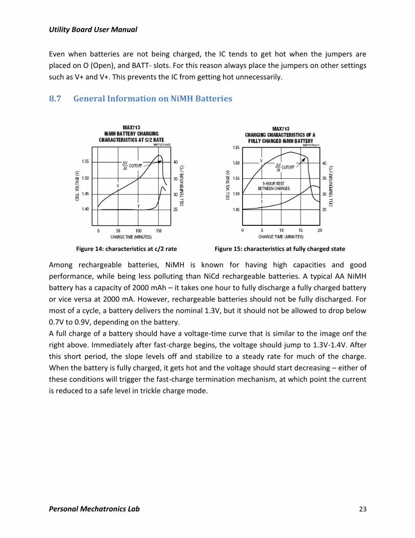
Figure 14: characteristics at c/2 rate Figure 15: characteristics at fully charged state
Even when batteries are not being charged, the IC tends to get hot when the jumpers are
placed on O (Open), and BATT- slots. For this reason always place the jumpers on other settings
such as V+ and V+. This prevents the IC from getting hot unnecessarily.
8.7 General Information on NiMH Batteries
Among rechargeable batteries, NiMH is known for having high capacities and good
performance, while being less polluting than NiCd rechargeable batteries. A typical AA NiMH
battery has a capacity of 2000 mAh – it takes one hour to fully discharge a fully charged battery
or vice versa at 2000 mA. However, rechargeable batteries should not be fully discharged. For
most of a cycle, a battery delivers the nominal 1.3V, but it should not be allowed to drop below
0.7V to 0.9V, depending on the battery.
A full charge of a battery should have a voltage-time curve that is similar to the image onf the
right above. Immediately after fast-charge begins, the voltage should jump to 1.3V-1.4V. After
this short period, the slope levels off and stabilize to a steady rate for much of the charge.
When the battery is fully charged, it gets hot and the voltage should start decreasing – either of
these conditions will trigger the fast-charge termination mechanism, at which point the current
is reduced to a safe level in trickle charge mode.

Utility Board User Manual
Personal Mechatronics Lab 24
Figure 16: Physical Location of the Oscilloscope module
9 Oscilloscope
The oscilloscope module takes in voltage input, carries out the analog-to-digital conversion, and
sends the data to a PC over a USB cable. Its maximum sampling frequency is 200kHz.
9.1 Instructions
A. Select PIC or OSC on the slide switch for PIC driver mode or oscilloscope mode.
B. Connect AUTO or MAN on the VREF jumper to select automatic or manual voltage
reference.
C. Connect the signal to Ch A or Ch B in the analog input terminal.
Utility Board User Manual
Personal Mechatronics Lab 25
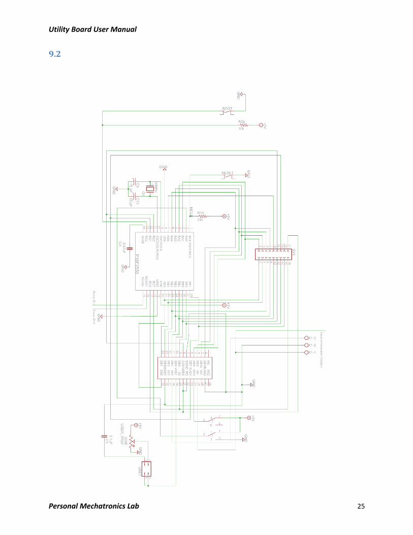
Figure 17: Schematic of the Oscilloscope module
9.2

Utility Board User Manual
Personal Mechatronics Lab 26
Schematic
9.3 Installation
Installation for the oscilloscope is very simple and consists of the following easy steps:
1. Install the oscilloscope application.
2. Ensure that the slide switch is set to OSC, not PIC.
3. Connect the Utility Board to the PC using the USB cable.
4. Apply power to the board and turn the power switch on.
5. The computer should automatically detect the board and install drivers within seconds.
6. Start the application.
7. Above the screen, the yellow light should turn on and it should display “Connected.”
8. Click on the play button to begin acquisition.
9. Select a time-base (TIME/DIV) appropriate for the expected frequencies of the signals.
The oscilloscope module can be broken down into three components: the PIC firmware, PC driver, and PC application.
9.4 PIC Firmware
The oscilloscope module uses a PIC18F2550 to control the data acquisition and USB
communication with the PC. The code is a modified version of Microchip’s HID device firmware
written in C, with custom code written for the oscilloscope data acquisition and transfer. The
user has the option of using this chip as a secondary micro-controller as there is a slide switch
that allows the user to run any custom user code written in the program memory of the PIC. In
order to reprogram the PIC to take advantage of this option, the user must use a programmer
such as the one on the DevBugger to program the PIC18 with the user code appended to the
USB oscilloscope code.
Address Program memory
0000 BTFSS PORTA, 0 Bootloader
BRA PIC //jumps to PIC
BRA OSC //jumps to OSC
OSC 1000 Oscilloscope code
PIC 8000 Custom user code
RA0
PIC18
5V
GND
Switch

Utility Board User Manual
Personal Mechatronics Lab 27
Figure 18: General overview of the firmware
9.5 Programming the PIC
The current version was implemented with a bootloader switch to enable onboard
programming. By pressing the switch down while powering on the board, the PIC enters the
bootloader which can be detected by the PC to enable programming. From this point, using
PICFUSB software, the PIC can be programmed with any hex code. This allows the user to
program user code very easily, making the utility board a simple programming board as well.
In order to program the PIC with user code, use “PDFUSB” software. Press the bootloader
switch with the software on to enter the bootloader. Once in the bootloader, select the hex file
that you want written to the pic. The hex file must include the firmware for the oscilloscope
and the user code appended to it. Follow the instructions below to create a programmable hex.
1. With User Code
a) Combine files 1-4 in the order to make a hex file with user code that causes B3 to blink.
b) The bootloader hex has already been edited to correct for end of file etc.
c) In order to use a different user code, simply set the .org to 0x2C00 and export starting at
0x2C00 also.
d) Remember there are 21502 instructions available for programming.
e) After this, the new user code can be combined in place of the included blinker code (the
blinker code is included as an example).
2. Without User Code
a) Combine files 1, 2, and 4 to create a programmable hex file without any user code.
b) Address starting from 0x2C00 will be empty
*0-FINAL is a hex file without user code and 0-FINAL (with user) is an example hex file with an
example user code that blinks the B3 pin. Install “Utility Board” to access these hex files.
9.6 PC Driver
The PIC firmware was written to communicate with the PC as an HID device. When the
oscilloscope is connected, the PC recognizes it as a Human Interface Device, which is a standard
device class recognized in most Windows platforms. The advantage of selecting the HID device
class is that there is no need for the user to acquire and install any custom drivers on the PC –
HID drivers should be included in any Windows-based PC, and detection and installation of the
device should be automatic and take mere seconds to complete.
9.7 PC Application
The graphical user interface of the oscilloscope is presented below. The layout is very simple: at
the centre of the application is the signal display region surrounded by 11 time-base options –

Utility Board User Manual
Personal Mechatronics Lab 28
Figure 19: The main window of the PC software application
equivalent to time per division. The top row’s 7 time-bases are for relatively low-frequency
signals, so they use real-time streaming mode. The bottom 4 time-bases works for high-
frequency signals, so they use block acquisition mode. To the right and left of the main, centre
column, the four channels are presented as quadrants. Typical oscilloscope parameters such as
VOLT/DIV and offset are controlled for each channel individually, independent from the other
channels.
Control options. The three buttons for acquisition control – stop, start, and pause – are located
below the main display region:
o The stop button halts acquisition if it has started, clears the screen, and resets the
internal application clock used for time-stamping when saving data to a text file.
o The start button begins or resumes acquisition depending on whether acquisition was
previously paused. In the latter case, the application resumes drawing from where it left
off if in streaming mode and the clock does not start from 0.
o Finally, the pause button halts acquisition, but does not clear the screen, nor does it
reset the clock. The start and pause buttons are enabled and disabled where
appropriate, based on the state of the application.
Saving. One of the features of the oscilloscope is the ability to save data to a text file as it is
acquired. In order to do this, the user must click save, opening a dialog in order to specify an
output location. The oscilloscope then enters recording mode, during which it records whatever
data is being displayed on the screen simultaneously to a text file with a timestamp. To exit

Utility Board User Manual
Personal Mechatronics Lab 29
recording mode, the user must click what was previously the save button. In recording mode,
stopping or pausing acquisition does not make it exit recording mode.
Channel parameters. Conveniently, each of the 4 quadrants represents a group of parameters
for a common channel. Within each channel group, there are 4 subdivisions – display select,
readings display, voltage per division, and calibration. Furthermore, each of the channels can be
enabled or disabled independently by clicking on the Channel label button:
o Display select allows the user to choose from 3 options. Selecting DC displays the
unchanged signal obtained for the particular channel, while the AC option filters out the
DC component (the signal average) to output the pure AC signal. Selecting GND displays
the equivalent of a constant, 0 V signal – this allows the user to quickly see visually what
offset the oscilloscope is using.
o The readings group shows real-time voltage and average voltage. Real-time voltage is
displayed much quicker than the average voltage since the average is not as responsive
to sudden changes, so it does not change quickly anyway. The array size for calculating
average is 2000 for streaming mode and 800 for block mode.
o The voltage per division group allows the user to select from 6 pre-selected common
voltages per division. Alternatively, the user can type a custom voltage per division for
more precision.
o The calibration group allows for adjustment of offset and amplitude for the channel. To
emphasize that these should be adjustment for calibration purposes, they are disabled
by default and must be enabled by clicking set.
File menu. There are three main drop-down menus, View, Reset, and Calibrate:
o The view menu provides a secondary way to enable and disable channels, as well as the
additional options of enabling or disabling all at once.
o The reset menu resets channels to default, individually or all at once.
o The calibrate menu provides an automatic method to calibrate offsets. Taring one or all
of the channels takes whatever voltage is being read for each channel and sets that
value as the new zero. Additionally, the user can also reset all offsets to default (no
offset).

Utility Board User Manual
Personal Mechatronics Lab 30
Figure 20: The three main drop-down menus
Figure 21: Data acquisition in streaming mode
9.8 Data Acquisition
There are two modes of operation under which the oscilloscope acquires data: The first is streaming mode. This mode acquires a sample roughly every millisecond and the
plot is a continuous display of points, although they are spaced relatively far apart in time. This
mode is slow because the PIC acquires a sample, then waits while the data is transmitted over
the USB bus to the PC. Thus, for every sample, the cycle of acquisition and transmission repeats
indefinitely.
The second is mode of operation is the block acquisition mode. This mode was developed to
allow users to see high frequency signals through higher resolution acquisition. Since the USB
transfer time is significant, the PIC does not wait after each sample is acquired for the data to
transfer to the PC; it fills up its memory banks with 196 consecutive samples, and then transfers
them all at once after acquiring 196 samples.
The resolution of the samples is only limited by the acquisition time – the time the AD
converter takes to convert the analog signal into binary numbers added to the time the PIC
takes to process the sample data and store it. The AD converter takes 4 µs and the PIC takes 2
µs for a total of 7 µs. The result is a maximum sampling rate of 166.6 kHz, significantly greater

Utility Board User Manual
Personal Mechatronics Lab 31
Figure 22: Data acquisition in block acquisition mode
than that of the streaming mode, which is roughly 1 kHz. Using Nequist theorem, this puts the
theoretical sampling frequency of the oscilloscope to half that, 83.33 KHz. With practical
drawbacks, the final frequency that can be handled by the oscilloscope is 28 KHz. Frequencies
above this can be handled but 100% accuracy is not guaranteed.
The time-bases in the milliseconds range use streaming mode and those in the microseconds
use block mode.
9.9 PIC Driver Mode
The oscilloscope module uses a PIC18, so it can double as a secondary PIC driver. In order to use
PIC driver mode, the user must set the slide switch from OSC to PIC with their code loaded onto
the PIC. For this purpose, there are 17 I/O pins available to the user as male headers.
PIC Driver Features:
Microcontroller: PIC18F2550
I/O pins: 17 available
Clock: 20 MHz
Peripherals: USB; I2C possible
In order to run custom user code on the oscilloscope’s PIC18F2550 with the oscilloscope still
usable, the user must append their code to the end of the oscilloscope hex file. To do this, the
user must do three things:
1. Modify the linker script for the user’s project so that the user’s code begins at line 2C00.
2. Take the user’s hex file, with its first line removed, and copy and paste it to the
oscilloscope hex file, with its last line removed (using notepad).
3. In order to program the code there are two options

Utility Board User Manual
Personal Mechatronics Lab 32
a. Use the DevBugger to program this code onto the Utility Board’s PIC18, just as
one would program the PIC16.
b. Press the Bootloader switch while power on and open PDFSUSB software. Press
the drop down menu and select the option. Load HEX file and press program
device to program on the utility board directly using USB.
If this is done successfully, the user can run both the custom code and the oscilloscope code
using the same firmware, by using the PIC-OSC switch in the oscilloscope module. It is beneficial
for the user to periodically check the RA0 pin – if it is high, the code should go to line 100,
where the oscilloscope code lies. This enables the ability for the user to alternate between PIC
and OSC modes using the switch, without turning off and turning on the power switch.
An easier solution from a programming standpoint is to burn only the user code onto the
oscilloscope’s PIC18 without appending it to the oscilloscope code. This is easier to do because
the user only needs to write their code and burn it onto the PIC just as they would with the
PIC16 without worrying about linker files or appending hexes. The disadvantage with this
approach, however, is that the user would not be able to use the oscilloscope and the custom
code using the same hex file. To switch back to the oscilloscope instead of the user’s custom
code, one would have to burn the oscilloscope’s original firmware back onto the PIC.

Utility Board User Manual
Personal Mechatronics Lab 33
Continuity Tester
Connect two wires
to the terminals
and use it to test
connection
between PCB
traces, wires, and
solder points.
Function Generator
Use either the TRIG or SQR
output terminal. If the former
is used, specify TRIG or SINE
using the switch. Select a
timescale jumper and use
potentiometers to adjust the
function.
Timescale
jumper
Minimum
frequency
Maximum
frequency
500 ms 1 Hz 10 Hz
50 ms 10 Hz 100 Hz
5 ms 100 Hz 1000 Hz
0.5 ms 1000 Hz 10000 Hz
0.05 ms 10000 Hz 100000 Hz
Parameter Description Range
Voltage Adjusts the top
voltage of the
square wave
0V to
10V
Offset Translates the
DC component
up or down
-10V to
10V
Frequency Fine
adjustment of
frequency
Min. to
max.
freq.
(see
above)
Duty cycle Changes the
shape of the
waveform
N/A
Amplitude Changes the
voltage range
of the
waveform
0V to
10V
Battery Charger
Connect the NiMH cell(s) and
a power source with a
voltage at least 1.5V greater
than the total voltage of the
battery and above 6V. Set the
PGM0 and PGM1 according
to the table below.
PGM0
V+ O
PG
M1
V+ 1 5
O 2 6
REF 3 7
BATT- 4 8
Oscilloscope
Set the VREF jumper to AUTO
to use the capacitor or MAN
to manually trim the MAN
VREF potentiometer and
control the reference
voltage. Connect the channel
input pins and the USB cable.
Utility Board QuickStart
IR Emitter Tester
Insert the emitter with the long
pin on the outside, and bend the
leads to bring it within 1 cm of
the detector.
Power Module
Connect board to a USB
port. Charging batteries
do not require switch to
be on. In order to
operate other modules
simply turn the switch on
to enable -12V and +5V.
Transistor Tester Insert the transistor in the correct NPN or PNP pin slots and observe the LED with the switch off and then on.
Switch off Switch on Transistor
LED off LED off BE short
LED off LED on Working
LED on LED on BC/CE short