Embed Size (px)
Citation preview
Embedded Solutions Page 1 of 58
DYNAMIC ENGINEERING 150 DuBois, Suite C Santa Cruz, CA 95060
(831) 457-8891 Fax (831) 457-4793 www.dyneng.com
[email protected] Est. 1988
User Manual
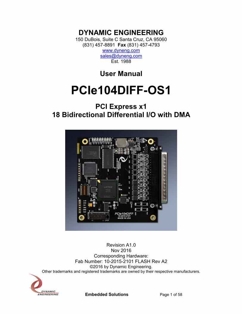
PCIe104DIFF-OS1
PCI Express x1 18 Bidirectional Differential I/O with DMA
Revision A1.0
Nov 2016 Corresponding Hardware:
Fab Number: 10-2015-2101 FLASH Rev A2 ©2016 by Dynamic Engineering.
Other trademarks and registered trademarks are owned by their respective manufacturers.

E m b e d d e d S o l u t i o n s P a g e 2 o f 5 8
PCIe104DIFF-OS1 PCI Express x1 with 18 differential IO
Dynamic Engineering 150 DuBois St. Suite C, Santa Cruz CA 95060
831-457-8891 831-457-4793 FAX
This document contains information of proprietary interest to Dynamic Engineering. It has been supplied in confidence and the recipient, by accepting this material, agrees that the subject matter will not be copied or reproduced, in whole or in part, nor its contents revealed in any manner or to any person except to meet the purpose for which it was delivered. Dynamic Engineering has made every effort to ensure that this manual is accurate and complete. Still, the company reserves the right to make improvements or changes in the product described in this document at any time and without notice. Furthermore, Dynamic Engineering assumes no liability arising out of the application or use of the device described herein. The electronic equipment described herein generates, uses, and can radiate radio frequency energy. Operation of this equipment in a residential area is likely to cause radio interference, in which case the user, at his own expense, will be required to take whatever measures may be required to correct the interference. Dynamic Engineering’s products are not authorized for use as critical components in life support devices or systems without the express written approval of the president of Dynamic Engineering. This product has been designed to operate with PCIe104 Modules and compatible user-provided equipment. Connection of incompatible hardware is likely to cause serious damage.

Embedded Solutions Page 3 of 58
PRODUCT DESCRIPTION 6
THEORY OF OPERATION 11
PROGRAMMING 14
PCIE104DIFF-OS1 ADDRESS MAP OVERVIEW 16
PCIE104DIFF-OS1 SIGNALING 17
PCIEDIFF104-OS1 SIGNAL SUMMARY TABLE 18
PCIEDIFF104-OS1 TIMING DIAGRAM 19
PCIeDIFF104-OS1 Timing summary table 19
PCIE104DIFF-OS1 RESETS AND CLOCKS 21
PCIE104DIFF-OS1 REGISTERS SUMMARY 23
PCIE104DIFF-OS1 GLOBAL REGISTERS 25
BOARD FEATURES 47
PCIE104DIFF-OS1 INTERRUPTS – APPENDIX A 50
MECHANICAL 53
APPLICATIONS GUIDE 53
ELECTRICAL 53
AC/DC TIMING 54

Embedded Solutions Page 4 of 58
INTERFACING 54
CONSTRUCTION AND RELIABILITY 55
THERMAL CONSIDERATIONS 55
WARRANTY AND REPAIR 56
Service Policy 56
Out of Warranty Repairs 56
For Service Contact: 56
SPECIFICATIONS 57
ORDER INFORMATION 58

Embedded Solutions Page 5 of 58
Figure 1 PCIe104DIFF-OS1 Block Diagram 9 Figure 2 PCIe104DIFF-OS1 FPGA Block diagram 10 Figure 3 PCIe104DIFF-OS1 Base Address Map 16 Figure 4 PCIe104DIFF-OS1 Signal Connections 17 Figure 5 PCIe104DIFF-OS1 Signal Summary 18 Figure 6 PCIe104DIFF-OS1 Signal Descriptions 19 Figure 7 PCIe104DIFF-OS1 Timing Diagram 19 Figure 8 PCIe104DIFF-OS1 DB37 Logic Signal Interface 20 Figure 9 PCIe104DIFF-OS1 Register Address Map 23 Figure 10 PCIe104DIFF-OS1 Register Address Map 24 Figure 11 PCIe104DIFF-OS1 Base Control Register 25 Figure 12 PCIe104DIFF-OS1 ID and Switch Bit Map 27 Figure 13 PCIe104DIFF-OS1 Status Port Bit Map 28 Figure 14 PCIe104DIFF-OS1 LED Control 28 Figure 15 PCIe104DIFF-OS1 Scratch Registers 29 Figure 16 PCIe104DIFF-OS1 Channel Control Register 31 Figure 17 PCIe104DIFF-OS1 Channel STATUS PORT 34 Figure 18 PCIe104DIFF-OS1 Write DMA pointer Register 38 Figure 19 PCIe104DIFF-OS1 TX FIFO data count Port 39 Figure 20 PCIe104DIFF-OS1 Read DMA pointer Register 40 Figure 21 PCIe104DIFF-OS1 TX FIFO data count Port 41 Figure 22 PCIe104DIFF-OS1 RX/TX FIFO Port 41 Figure 23 PCIe104DIFF-OS1 TX ALMOST EMPTY LEVEL Register 42 Figure 24 PCIe104DIFF-OS1 RX ALMOST FULL LEVEL Register 42 Figure 25 PCIe104DIFF-OS1 Channel Transmit Control Register 43 Figure 26 PCIe104DIFF-OS1 TX Hold OFF Register 44 Figure 27 PCIe104DIFF-OS1 Channel Rx Control Register 45

Embedded Solutions Page 6 of 58
Product Description
PCIe104DIFF is part of Dynamic Engineering’s PCIe104 family of modular I/O components. PCIe104DIFF card provides up to 18 differential IO through a DB37 connector along with FPGA support in a compact package. LVDS and RS485 transceivers can populate the IO. Matched length, controlled impedance connections. All parts are at least industrial temperature. Each IO may be configured as a receiver/input or transmitter/output. Of the 18 I/O, 4 are connected to FPGA pins that can be used as high speed clock inputs. The PCI Express link is a by one (x1) link that is fully compliant to PCI Express 1.1 revision of the PCI-SIG specification and as such can operate in any compliant PCIe Gen1, Gen2, Gen3, or Gen4 position. SDRAM is attached to the Lattice FPGA. The SDRAM can be configured as needed to make a large RAM or FIFO space. 16Mx16 is the device size. A Cypress 22393 PLL is provided on the PCIe104DIFF to allow users to create specific frequencies with which to operate the state-machines and I/O (see Board Features section for details). An 8-bit "dip switch" is provided on the PCIe104DIFF for user-defined purposes. The switch configuration is readable via a memory-mapped I/O port. We envision the switch being used for software configuration control, board identification or test purposes. PCIe104DIFF has 8 user LED’s which can be programmed to turn on using software. The hardware supports full bidirectional DMA from/to the PCI Express Host to/from the Target Receiver/Transmitter interfaces. The DMA engines use high bandwidth FIFO’s to optimize simultaneous bidirectional DMA transfers and provide interface data rate-matching. For the “OS1” version the IO is LVDS, the base clock rate is 150 MHz, the SDRAM is included and the PLL is currently unused. The transmitter and receive data paths both have approximately 18K bytes of FIFO storage inside the FPGA. Additionally, PCIe104DIFF-OS1 implements a 32 Mbyte (16Meg x 16bit wide) SDRAM which can be enabled and configured to create selectable sizes of data storage to be added to either the transmitter or receiver data paths.

Embedded Solutions Page 7 of 58
In addition to DMA the hardware also supports direct access software controlled read/write access to internal registers and the high bandwidth FIFO ports. PCIe104DIFF-OS1 supports multiple interrupts with individual mask bits. An interrupt force bit is available to aid in software development. All the interrupts are mask-able. The masked interrupt output signals are tied together and if asserted will generate either a PCI Express MSI or INTA# as provided by the system. Power-on PCIe PERST# reset is used to reset the entire PCIe104DIFF-OS1. Additionally Reset bits are provided to reset different parts of the logic. To meet the PCI Express specification requirement for PCIe core initialization within 100mS from PERST# de-assertion; PCIe104DIFF implements a 16 bit wide 90ns Flash in conjunction with a CPLD to configure the FPGA via its parallel configuration port. With this architecture, PCIe104DIFF beats this aggressive specification by a comfortable margin. Dynamic Engineering can provide Windows, Linux and VxWorks drivers for the PCIe104DIFF. The Lattice FPGA is re-configurable by loading a new programming file into the FLASH storage device using the PCIe104DIFF’s JTAG port and Lattice programming software and compatible USB to JTAG hardware. If your project can benefit from a "non-standard" implementation, or features that we have not thought of, or implemented yet please let us know.

Embedded Solutions Page 8 of 58
Feature List Summary • PCI Express Gen1, Gen2, Gen3, or Gen4 slot operable and compliant • High speed user transmit/receive differential IO – 150MHz + • Bidirectional DMA – Independent Transmit and Receive DMA channels • 18K bytes of High Bandwidth FIFO storage for both Transmit and Receive channels • 32 Mbyte SDRAM – configurable for either or both the transmit or receive data paths • MSI and INTA# Interrupt support • High Performance Lattice ECP3 FPGA • 18 Configurable user IO – 4 can be clock inputs • PLL with 2 independently programmable clocks connected to FPGA • Interface with matched length, impedance controlled traces between IO and DB37 connector • 8 position "DIP Switch" • 8 User LED's • Ability to add new client features with ease - via Flash update • Windows, Linux & VxWorks drivers As Dynamic Engineering adds features to the hardware we will update the PCIe104DIFF page on the Dynamic Engineering website. If you want some of the new features, and have already purchased hardware, you can download the Flash update and use the tools provided to update the Flash via the JTAG port. Or you may send the board back and Dynamic Engineering will update the Flash. A nominal fee is required for this service. The basic PCIe identifying information will not change with the updates, including the PCIe Revision ID field which is set to 0x01. To allow configuration control a Version ID register is provided at offset 0x004 to indicate the current code revision of the FPGA. Each devices revision ID has a major and minor field. The major field is updated with new client releases. The minor is used internally for development purposes and in some cases with specialized client releases. Our drivers make the revision information available as part of the board info. Dynamic Engineering provides drivers for PCIe104DIFF-OS1. The drivers detect the card and communicate with the OS to get the memory, interrupts etc. assigned to the board.

Embedded Solutions Page 9 of 58
PCIe104DIFF-OS1 Block Diagram
5V & 3.3V
from PCI Express “Super Buck” used to
generate 1.2V from 5V
CPLD Parallel FPGA Loader
PERp/n0
16 bit – 90ns FLASH
JTAGHeader
32MHzOSC
PETp/n0
Lattice ECP3 FPGA
P5VGOOD
Parallel CFG & Data
Switch Inputs
TDO
PCIe REFCLK +/-
5V 3.3V 1.2V
USERDIP Switch
USER LED [7:0]
PCI Expressx1
Interface
Multiplexorused to connect to
either theTop or Bottom
connector
TDI
TDITDO
Lattice ECP3 FPGA
PCIExpress
CorePERST#
IO[17:0]IO
LED[7:0]
DIR[17:0]DIR
TERM[17:0]TERM
``
DifferentialTransceivers
LVDS/485or
compatible
IO_P[17:0]
IO_N[17:0]
``
32 MbyteSDRAM
16bitdata bus
SDRAMInterface
I2C
50MHzOSC
CY22393
TriplePLLCLKA
CLKB
``
DB37Right Angle
Pin-Board Lock4-40 Cable
MountConnector
PLLREF
Figure 1 PCIe104DIFF-OS1 Block Diagram

Embedded Solutions Page 10 of 58
PCIe104DIFF-OS1 FPGA Block Diagram
FPGA Block Diagram to be created
Figure 2 PCIe104DIFF-OS1 FPGA Block diagram

Embedded Solutions Page 11 of 58
Theory of Operation
PCIe104DIFF-OS1 functions as an IO controller that is controlled by a PCI Express Host, as such the PCIe104DIFF-OS1 is defined to be a PCIe Endpoint. As an Endpoint the PCIe104DIFF-OS1 is downstream from the Host/Root Complex which detects it and configures it during the enumeration process using PCIe configuration read and write packets. PCIe104DIFF-OS1 requests a total of 4KB from the Host who provides a 4KB space using PCIe104DIFF-OS1’s BAR0 during the enumeration process. The PCIe104DIFF-OS1 handles all accesses within its 4KB space. The 4KB of space is used to access the PCIe104DIFF’s registers, FIFO’s, or external logic such as the LED output pins or dip switch inputs. If a packet is received with an address outside the PCIe104DIFF-OS1’s BAR0 space it is discarded, credits are updated, and an unsupported request PCIe packet is returned to complete the transaction. PCIe104DIFF-OS1 uses a Lattice semiconductor ECP3 Family FPGA and utilizes Lattice’s PCI Express Endpoint Core IP which is compliant to PCI-SIG PCI Express 1.1 Base Specifications. The core handles the PCIe Physical and Data Link Layer requirements and provides an extensive interface which the PCIe104DIFF-OS1 interacts with to receive or transmit Transaction Layer Packets (TLPs) and communicate and/or update available flow control credits. All Transaction Layer Packets coming from the PCIe Core that are within BAR0 space are written into a receive packet FIFO. Upon detecting a packet is in the receive FIFO it is immediately read out to be processed, i.e. execute a read or write access to a memory location within its 4KB space. The FIFO’s are sized and PCIe104DIFF-OS1 advertises credits such that multiple access packets can be pending. Once a PCIe104DIFF-OS1 access has completed processing a write or read, the appropriate credit updates will be accumulated and sent to the core which will create Flow Control DLL packet(s) to inform/update the Host that more space/credit is available inside the PCIe104DIFF-OS1.

Embedded Solutions Page 12 of 58
For transmission of data out the the IO outputs (TX) Host data is transferred into the transmit FIFO via DMA transfers from host memory. The user defined output state machine reads the data from the FIFO and applies the user protocol before transmitting. On the receive side the data flows into the FPGA via the user defined IO inputs (RX), then is processed and stored in the receive FIFO. The data is read from the receive FIFO by the PCIe control state-machine and moved into host memory via DMA transfers. If the SDRAM is enabled, the path to the Transmit or from the Receive local FIFO’s is indirect. In the TX path the PCIe DMA transfers data into the SDRAM TX DMA FIFO. The data stored in the SDRAM is then moved to the output FIFO. The SDRAM controller uses the state of the FIFO’s and SDRAM to determine when to move data or not. The TX state-machine reads from the TX IO FIFO and converts/encodes the data per the users design specification and then transmits (TX’s) the data out the IO(s). The PCIe104DIFF-OS1 TX Data path uses FIFO’s to convert between the 125 MHz PCIe interface, the internal logic clock domain, and then into the users defined TX clock rate. The receive path is similar with the receiver controller using a rate matching local FIFO. If the SDRAM is enabled the RX IO FIFO is read by the SDRAM controller and moved to the SDRAM. From the SDRAM, data is loaded to the SDRAM RX DMA FIFO for transfer to the internal logic clock domain, then to the PCIe/host memory domain. The SDRAM controller block has FIFO counts available to allow the TX and RX SM to properly interact with the FIFO’s built into the SDRAM controller. The SDRAM controller automatically uses page mode and single transfers based on data and space available. PCIe104DIFF-OS1 operates at 125 MHz within the SDRAM controller, internal FIFO ports and SDRAM. The SDRAM controller has bypass transfer units which if enabled move data directly from the SDRAM TX DMA FIFO to the SDRAM TX IO FIFO and similarly from the SDRAM RX IO to the SDRAM RX DMA FIFO’s. Each bypass is independent which allows all of the SDRAM to be tied to one port or the other. The SDRAM controller has an arbitration unit which determines on a round-robin basis which channel to service next. When an operation completes the arbiter looks at each of the other options before checking the same channel again. The logic has skip-ahead to save states when a channel is disabled. The TX and RX have load and unload operations with separate enables to allow the software to configure TX only, RX only, TX load before start-up etc. The design includes a FIFO mode and a retransmit mode. The retransmit mode has the ability to

Embedded Solutions Page 13 of 58
send a header, body, and tail. The FIFO mode makes the SDRAM act like a FIFO and is the mode used in the PCIe104DIFF-OS1. Please see the programming section for more details. The full bandwidth of the PCIe link is utilized during DMA transfers. There is some overhead on the PCIe side, which will limit the actual sustainable transfer rate somewhat compared to the theoretical limit. Using SDRAM one can calculate how long the OS can "go away" without RX data being transferred out before data over-runs the FIFO or under-running the FIFO when used for transmit. With Windows® and other high level OS based system the OS can neglect data movement due to other requirements - dealing with the keyboard or HDD for example. Having adequate storage can make a big difference in system performance.

Embedded Solutions Page 14 of 58
Programming
PCIe104DIFF-OS1 is tested in a Linux and Windows environment. We use the Dynamic Engineering Driver to do the low level accesses to the hardware. We use MS Visual Studio in conjunction with the driver to write our test software [under Windows]. We use Ubuntu for Linux development. The drivers take care of discovery and the UserAp allows the client to select which installed board is selected for use. In addition a menu is available to allow test selection and operation of the Windows based reference applications. If you are writing your own driver it is suggested to get the engineering kit and the Linux version of the SW. Usually the code defines and perhaps some of the code can be reused in your effort. The PCIe104DIFF registers offsets are relative to the base address. The base address is assigned to the PCIe104DIFF by the system using the PCIe BAR configuration registers. Once the initialization process has occurred, and the system has assigned addresses to the PCIe104DIFF card the software will need to determine what the address space is for the PCI interface [BAR0]. The offsets in the address tables are relative to the system assigned BAR0 base address. Programming the PCIe104DIFF requires only the ability to read and write data in the host's PCI space. If needed, the next step is to initialize and configure the PCIe104DIFF-OS1’s external PLL. Clocking requirements for many applications can be meet using the PLL’s internal to the Lattice ECP3 FPGA. The external PLL’s programmabiltiy, multiple different clock outputs, and range of settings provides a wide range of capabilities which should be sufficent to meet any applications needs. PCIe104DIFF implements a Cypress CY22393. Cypress CyberClocks software can be used to create new .JED files if desired. The driver comes with a .JED file prepared. “PCIe104DIFF-OS1IFF.JED” The driver has a utility to load the PLL and read back. The reference application software has an example of the use of PLL programming. The reference application software also includes XLATE.c which converts the .JED file from the CyberClocks tool to an array that can be programmed into the PLL.

Embedded Solutions Page 15 of 58
For Windows™ and Linux systems the Dynamic Drivers can be used. The driver will take care of finding the hardware and provide an easy to use mechanism to program the hardware. The Driver comes with reference software showing how to use the card and reference frequency files to allow the user to duplicate the test set-up used in manufacturing at Dynamic Engineering. Using simple, known to work routines is a good way to get acquainted with new hardware. To use the PCIe104DIFF-OS1 specific functions such as the Channel Control, and PLL interface plus DMA will need to be programmed. To use DMA, memory space from the system should be allocated and the link list stored into memory. The location of first DMA descriptor in the link list is written to PCIe104DIFF-OS1 to start the DMA. Please refer to the Burst IN and Burst Out register discussions. Some applications users may want the FIFO being full or close to it when the DMA transfer is started, or may want at least the Packet loaded if shorter than the FIFO size. To further facilitate continuous transmission the Ready Level is programmed to the number of LW desired to be in the Output FIFO before starting up. This allows the Transmitter to be enabled and start at the programmed level automatically. DMA can be programmed with a specific length. The length can be as long as you want within standard memory limitations. At the end of the DMA transfer the Host will receive an interrupt. With non-blocking DMA the application will be told how many bytes were transferred. With blocking the thread will wait for the programmed amount to be available in host memory before providing the interrupt. The receiver can be stopped and the FIFO reset to clear out any extra data captured. For on-the-fly processing multiple shorter DMA segments can be programmed; at the interrupt restart DMA to point at the alternate segment to allow processing on the previous one. This technique is sometimes referred to as “ping-pong”. Please see the channel control register bit maps for more information.

Embedded Solutions Page 16 of 58
PCIe104DIFF-OS1 Address Map Overview
Registers Offset Size
Global 0x000 – 0x04F 80 Bytes
Channel0 0x050 to 0x0EF 160 Bytes
Channel1 0x0F0 to 0x18F 160 Bytes
Reserved 0x190 to 0xFFF 3696 Bytes Figure 3 PCIe104DIFF-OS1 Base Address Map
The address map provided is for the local decoding performed within PCIe104DIFF-OS1. The addresses are all offsets from a base address. The base address, BAR0 is provided by the host in which the PCIe104DIFF-OS1 is installed. See register section for detailed descriptions of all the registers in the PCIe104DIFF-OS1. The host system will enumerate to find the assets installed during power-on initialization. The PCIe104DIFF-OS1’s Vendor ID = 0xDCBA and Device ID = 0x005E. Third party utilities can be useful to see how your system Memory Map is configured. The interrupt level expected and style is also set in the registry. Dynamic Engineering recommends using the Dynamic Engineering Driver to take care of initialization and device registration. Once the initialization process has occurred and the system has assigned an address range to the PCIe104DIFF-OS1 card, the software will need to determine what the address space is. We refer to this address as base in our software. The next step is to initialize the PCIe104DIFF-OS1 by configuring the relevant bits in the control and interrupt registers. Optionally additional registers such as the Switch and LED control may also be read or configured respectively at this point. The user switch can be used to deterministically select the intended PCIe104DIFF-OS1 module when multiple hosts/carriers with multiple modules are implemented. Setting the switches to different known values and reading the switch values enables remapping the handles for the hosts/carriers to provide an automatic mechanism to be sure your application software is communicating with the correct PCIe104DIFF-OS1 when multiple PCIe104DIFF-OS1’s of the same type are available within the system.
Embedded Solutions Page 17 of 58
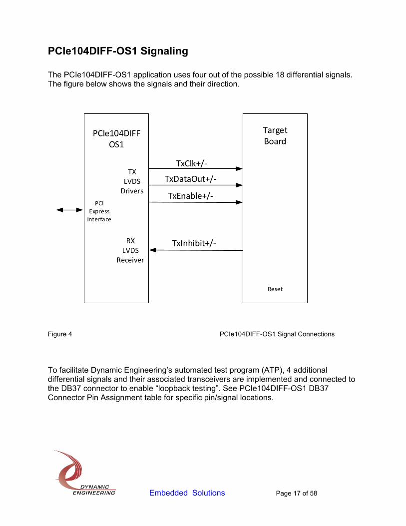
PCIe104DIFF-OS1 Signaling
The PCIe104DIFF-OS1 application uses four out of the possible 18 differential signals. The figure below shows the signals and their direction.
PCIe104DIFFOS1
TargetBoard
TXLVDS
Drivers
TxInhibit+/-
TxClk+/-
TxDataOut+/-
Reset
RXLVDS
Receiver
PCIExpress
Interface
TxEnable+/-
Figure 4 PCIe104DIFF-OS1 Signal Connections
To facilitate Dynamic Engineering’s automated test program (ATP), 4 additional differential signals and their associated transceivers are implemented and connected to the DB37 connector to enable “loopback testing”. See PCIe104DIFF-OS1 DB37 Connector Pin Assignment table for specific pin/signal locations.

Embedded Solutions Page 18 of 58
PCIeDIFF104-OS1 Signal summary table
Signal Direction Description
TxClk To Target Transmit Clock - This is the transmit interface clock. It runs at 150MHz. TxDataOut and TxEnable are clocked out of the PCIe104DIFF on the rising edge of this clock/signal.
TxDataOut To Target Transmit Data - This is the serial Data signal. Data is valid on the rising edge of TxClk when TxEnable is asserted true high.
TxEnable To Target Transmit Enable – Transitions on the rising edge of TxClk. When true high on a rising TxClk edge TxDataOut is valid.
TxInhibit From Target Transmit Inhibit – Asserted by the Target to pause the transfer. When asserted during a transfer the PCIe104DIFF-OS1 will pause the transfer by de-asserting the TxEnable signal when it finishes transferring the remaining bits of the LW/32bits it is currently transferring. The transfer will resume once the TxInhibt is deasserted. If TxInhibit is asserted before a transfer starts the PCIe104DIFF will not start the transfer until the TxInhibit is de-asserted.
Figure 5 PCIe104DIFF-OS1 Signal Summary

Embedded Solutions Page 19 of 58
PCIeDIFF104-OS1 Timing Diagram
TxClk
TxDataOutor
TxEnable
Clock to
OutDelay
Input SignalSetupTime
Input SignalHoldTime
Figure 6 PCIe104DIFF-OS1 Timing Diagram
PCIeDIFF104-OS1 Timing summary table
Signal Direction Timing Description
TxClk To Target At 150MHz this clock has a period of 6.667ns. Before being output the TxClk is adjusted inside the design with the goal to provide equal setup and hold time for both the TxDataOut and TxEnable signals (relative to the clock).
TxDataOut and
TxEnable
To Target The setup and hold in percentages of the period. Setup = 60% of period Hold = 30% of period Signal transition = 5% of period (Both edges = 10%). Notes: Clock and Signals measured externally at the transmitter; With trace matched signaling signals would be expected to track equally to their destination. Users should check signal timing and quality at the receivers.
TxInhibit From Target Transmit Inhibit is an input to the PCIe104DIFF-OS1. There are no timing requirements for this signal as it is synchronize to the TxClk inside the design before use.
Figure 7 PCIe104DIFF-OS1 Signal Descriptions

Embedded Solutions Page 20 of 58
PCIe104DIFF-OS1 DB37 Connector Pin Assignment
The figure below gives the pin assignments for the DB37 connector on the PCIe104DIFF-OS1. Pins marked n/c below are not used for the PCIe104DIFF-OS1 implementation.
IO_0p (RxClk+) IO_0m (RxClk-) 1 2 IO_1p (RxDataIn+) IO_1m (RxDataIn-) 20 21 IO_2p (RxEnable+) IO_2m (RxEnable-) 3 4 IO_3p (TxInhibit+) IO_3m (TxInhibit-) 22 23 IO_4p (TxClk+) IO_4m (TxClk-) 5 6 IO_5p (TxDataOut+) IO_5m (TxDataOut-) 24 25 IO_6p (TxEnable+) IO_6m (TxEnable-) 7 8 IO_7p (RxInhibitOut+) IO_7m (RxInhibitOut-) 26 27 IO_8p (unused) IO_8m (unused) 9 10 IO_9p (unused) IO_9m (unused) 28 29 IO_10p (unused) IO_10m (unused) 11 12 IO_11p (unused) IO_11m (unused) 30 31 IO_12p (unused) IO_12m (unused) 13 14 IO_13p (unused) IO_13m (unused) 32 33 IO_14p (unused) IO_14m (unused) 15 16 IO_15p (unused) IO_15m (unused) 34 35 IO_16p (unused) IO_16m (unused) 17 18 IO_17p (unused) IO_17m (unused) 36 37 GND* 19
Figure 8 PCIe104DIFF-OS1 DB37 Logic Signal Interface
Signal Name
FPGA/Differential Direction
Differential IO/Instance
FPGA Pin
RxClk Input/Receiver IO_0/U5 N19
RxData Input/Receiver IO_0/U6 R21
RxEnable Input/Receiver IO_0/U7 R16
TxInhibit Input/Receiver IO_0/U8 N18
TxClk Output/Driver IO_0/U9 L19
TxDataOut Output/Driver IO_0/U10 J20
TxEnable Output/Driver IO_0/U11 H21
RxInhibitOut Output/Driver IO_0/U12 E22

Embedded Solutions Page 21 of 58
PCIe104DIFF-OS1 Resets and Clocks
PCI Express Reset (PERST#) summary There are two types of resets in PCIe, both of which are supported by the PCIe104DIFF-OS1, they are:
Fundamental Reset (cold or warm) – assertion of PERST# o Cold - Power applied to a cold (non-powered) system. o Warm – Power is up/good before & during assertion of PERST#.
Hot Reset – TS1 Ordered-Sets sent with bit [0] of symbol 5 asserted for 2ms. Per the PCIe specification:
The minimum PERST# assertion time is 100ms from the time power is stable. o In order to be configured and ready for enumeration before PERST# is de-
asserted PCIe104DIFF-OS1 downloads the FPGA configuration file from a parallel Flash.
PERST# signal is asserted and de-asserted asynchronously. PCIe104DIFF-OS1 Reset bits In addition to the global wide reset provided by the PCI Express PERST# assertion the PCIe104DIFF-OS1 provides the following three register bits to reset different part of the logic. ResetInt - PLL_Reset_BigEndianDma Register bit [15] – this bit is combined with the system reset to create an internal reset. Setting this bit ‘1’ will cause a board level reset with all features except the PCIe core, base control register, and certain clocking assets. Default and operational setting is ‘0’. Receive/Transmit FIFO Reset – Channel Control Register bit [1] / [0] – When set to a one, the transmit and/or receive FIFO’s will be reset. In addition the Transmit/Receive State Machines and associate logic in there data paths are also reset.

Embedded Solutions Page 22 of 58
PCIe104DIFF-OS1 Clocks The PCIe104DIFF-OS1 has multiple clock domains. Domains that communicate with each other do so through FIFOs. The total number of clocks used is application specific. The clock domains used for the PCIe104DIFF-OS1 are:
PCI Express Reference clock – Standard External PCIe Specified 100MHz clock used by the Lattice PCI Express core.
Internal 125MHz PCIe core interface clock - Used inside the FPGA.
Internal 125MHz SDRAM clock - Derived from external 50MHz OSC or PLL.
Internal Logic clock derived from external OSC or PLL - Used for internal fabric logic inside the FPGA. The fabric logic enables any logic/clock domain to communicate with any other logic/clock domain, its frequency is application specific.
TX IO Clock – Driven out by the PCIe104DIFF-OS1, derived from OSC or PLL. Designs up to 150MHz have been achieved, higher frequencies are possible.
RX IO Clock – Received by the PCIe104DIFF-OS1.150MHz operation has been achieved, higher frequencies are possible. The RX IO Clock is only used for Loopback testing in the ATP for the PCIe104DIFF-OS1.
The external Cypress PLL is programmed with the output file generated by the Cypress programming tool. [CY3672 R3.01 Programming Kit or CyberClocks R3.20.00 Cypress may update the revision from time to time.] The .JED file is used by the Dynamic Driver to program the PLL. Programming the PLL is fairly involved and beyond the scope of this manual. For clients writing their own drivers it is suggested to get the Engineering Kit for this board including software, and to use the translation and programming files ported to your environment. This procedure will save you a lot of time. For those who want to do it themselves the Cypress PLL in use is the 22393. The output file from the Cypress tool can be passed directly to the Dynamic Driver [Linux or Windows] and used to program the PLL without user intervention. The reference frequency for the PLL is 50 MHz.

Embedded Solutions Page 23 of 58
PCIe104DIFF-OS1 Registers Summary
PCIe104DIFF-OS1 register map – Offset 0x000 to 0x18F 80 bytes for Global Registers
Offset Register Description
0x000 PLL, Reset, BigEndianDma Control
0x004 Switch, Revision & ID Switch Status, Design Rev and ID #’s
0x008 Interrupt Status Interrupt Status
0x00C LED Control LED control – bits [7:0] correspond to LED[7:0]
0x010 Scratch 0 User scratch register 0
0x014 Scratch 1 User scratch register 1
0x018-4F Reserved -
Channel0 Registers - 160 bytes
Offset Register Description
0x050 Channel Control Channel Control
0x054 Channel Status Channel Status
0x058 – W Channel WR_DMA_PNTR Write to start Host to TX DMA
0x058 – R Channel TX_FIFO_COUNT # of LW’s in TX FIFO
0x05C – W Channel RD_DMA_PNTR Write to start RX to Host DMA
0x05C – R Channel RX_FIFO_COUNT # of LW’s in RX FIFO
0x060 Channel FIFO LW Access W/R single LW to/from TX/RX FIFO
0x064 Channel TX_AMT_LVL Sets when TX almost-empty status bit is set
0x068 Channel RX_AFL_LVL Sets when RX almost-full status bit is set
0x06C Channel TX Control TX Control Bits
0x070-07B Reserved -
0x07C Channel TX Ready Sets # of LW’s in TX SM FIFO to start transfer
0x080 Reserved -
0x084 Channel RX Control RX Control Bits
0x088-9F Reserved -
0x0A0-0EF Memory & Loopback Memory and Loopback Test Registers
Channel1 Registers - 160 bytes
Offset Register Description
0x0F0-18F Identical to Channel0 Reserved for Test Only Figure 9 PCIe104DIFF-OS1 Register Address Map

Embedded Solutions Page 24 of 58
PCIe104DIFF-OS1 register map – Offset 0x0A0 to 0D3 80 bytes for Memory and Loopback Registers
Offset Register Description
0x0A0 Channel RX_MEM_A Receive Address A
0x0A4 Channel TX_MEM_A Transmit Address A
0x0A8 Channel SET_MEM Spare – Reserved for Direct Memory Set
0x0AC Channel RX_MEM_B Receive Address B
0x0B0 Channel TX_MEM_B Transmit Address B
0x0B4 Channel RX_MEM_C Receive Address C
0x0B8 Channel TX_MEM_C Transmit Address C
0x0BC Channel RX_MEM_D Receive Address D
0x0C0 Channel TX_MEM_D Transmit Address D
0x0C4 Channel RX_LOOP_CNT Receive Body Loop Count [7:0]
0x0C8 Channel TX_LOOP_CNT Transmit Body Loop Count [7:0]
0x0CC Channel RX_SDRAM_CMD Receive SDRAM Control Register [7:0]
0x0D0 Channel TX_SDRAM_CMD Transmit SDRAM Control Register [7:0] Figure 10 PCIe104DIFF-OS1 Register Address Map

Embedded Solutions Page 25 of 58
PCIe104DIFF-OS1 Global Registers
Global/Board Level Registers - offsets 0x00 to 0x4F
PLL_Reset_BigEndianDma
[0x000 Main Control Register Port read/write]
DATA BIT DESCRIPTION 31-21 spare 20 bit 19 read-back of pll_dat register bit 19 pll_dat [write to PLL, read-back from PLL] 18 pll_s2 17 pll_sclk 16 pll_en 15 ResetInt 14-1 spare 0 BigEndianDma
Figure 11 PCIe104DIFF-OS1 Base Control Register
This is the base control register. The features common to all channels are controlled from this port. Unused bits are reserved for additional new features. Unused bits should be programmed ‘0’ to allow for future commonality. BigEndianDma : ‘0’ disables this option. ‘1’ enables this option. When operating with a Big Endian platform and using PCIe accesses DMA can have challenges. The register accesses directly over the PCIe bus are usually taken care of automatically with byte swapping within the CPU or PCI interface on the CPU. DMA data is written to or read from the local memory and is not swapped. The direct read/write from memory ends up with scrambled data [relative to little endian definitions]. Setting this bit will byte reverse the data for the DMA path into the TX and out of the RX FIFO’s only. Register accesses are not affected. 31-24, 23-16, 15-8, 7-0 7-0, 15-8, 23-16, 31-24 byte swapping pattern implemented. ResetInt is combined with the system reset to create an internal reset. Setting this bit ‘1’ will cause a board level reset with all features except the PCI core, base control register, and certain clocking assets. Default and operational setting is ‘0’. pll_en: When this bit is set to a one, the signals used to program and read the PLL are enabled.

Embedded Solutions Page 26 of 58
pll_sclk/pll_dat : These signals are used to program the PLL over the I2C serial interface. Sclk is always an output whereas Sdata is bi-directional. This register is where the Sdata output value is specified or read-back. pll_s2: This is an additional control line to the PLL that can be used to select additional pre-programmed frequencies. Set to ‘0’ for most applications. The PLL is programmed with the output file generated by the Cypress programming tool. [CY3672 R3.01 Programming Kit or CyberClocks R3.20.00 Cypress may update the revision from time to time.] The .JED file is used by the Dynamic Driver to program the PLL. Programming the PLL is fairly involved and beyond the scope of this manual. For clients writing their own drivers it is suggested to get the Engineering Kit for this board including software, and to use the translation and programming files ported to your environment. This procedure will save you a lot of time. For those who want to do it themselves the Cypress PLL in use is the 22393. The output file from the Cypress tool can be passed directly to the Dynamic Driver [Linux or Windows] and used to program the PLL without user intervention. The reference frequency for the PLL is 50 MHz.

Embedded Solutions Page 27 of 58
ID, Revision & Switch
[$004 Switch and Design number port read only]
DATA BIT DESCRIPTION 31-28 Design Revision – Major 27-24 Design Revision – Minor 23-16 Design ID 15-8 PCIe Core Revision 7-0 DIP switch
Figure 12 PCIe104DIFF-OS1 ID, Revision and Switch Bit Map
The DIP Switch is labeled for bit number and ‘1’ ‘0’ in the silk screen. The DIP Switch can be read from this port and used to determine which PCIE104DIFF-OS1 physical card matches each PCIe address assigned in a system with multiple cards installed. The DIPswitch can also be used for other purposes – software revision etc. The switch shown would read back 0x12.
The Design Revision has a major and minor field (16 revisions each) the current Design Revision is 0x12. The Design Revision will be updated for major changes to allow drivers to differentiate between revisions and applications. The Design ID field indicates one of 256 possible designs. The PCIE104DIFF-OS1 Design ID is 0x01. The PCIe Core revision is 0x01

Embedded Solutions Page 28 of 58
Interrupt Status
[$008 Board level Status Port read only]
DATA BIT DESCRIPTION
31-21 set to ‘0 20 Reserved 19-17 set to ‘0 16 Reserved 7-2 set to ‘0’, reserved for additional channels 1 Unmasked Ch1 Interrupt 0 Unmasked Ch0 Interrupt
Figure 13 PCIe104DIFF-OS1 Status Port Bit Map
Channel Interrupt – The local interrupt status from the channel. Each channel can have different interrupt sources. DMA Write, DMA Read , IntForce or TX/RX request are typical sources. Polling can be accomplished using the channel status register and leaving the channel interrupt disabled. If needed this register will contain PLL lock bit(s) status, the info highlighted below will be updated upon the next release of the manual. The OS1 design only uses the external 50MHz OSC and as such PLL lock info isn’t relevant. Please note: the power up sequence should be to discover the card, initialize at the base level – program PLL, wait for lock in Base Status etc. Then check lock status in the channel and potentially check the frequency too. Once the channel is locked to the external clock proceed with initialization of the transmitter.

Embedded Solutions Page 29 of 58
LED Control
[$00C LED port read/write ]
DATA BIT DESCRIPTION 31-28 Reserved 27-24 LED Select 0000 = Link and board status 0001 = User LED Control [7:0] – bits [7:0] of this register. 0010 = User switch settings – ‘1’ on pin turns on LED 0011 = Reserved - Test Mode LED’s 0100 to 0111 = Reserved 1000 = Posted Header Credits – available from host 1001 = Non Posted Header Credits – available from host 1010 = Completion Header Credits – available from host 1011 = Posted Data Credits – available from host 1100 = Non Posted Data Credits – available from host 1101 = Completion Data Credits – available from host 1110 to 1111 = Reserved 23-8 Reserved 7-0 LED Register bits – bits[7:0] corespond to LED’s[7:0]
Figure 14 PCIe104DIFF-OS1 LED Control Bit Map
LED Select: Four bits that select what values control the 8 user LED’s. The default LED Select value is 0x00 (Link and board status). LED Select = 0000 - Link and board status When LED’s[3:0] are on after boot, the PCIe link is up/functional, LED’s on indicate: LED[3] - Data Link Layer is up; LED[2] - L0 – L0 state has been reached; LED[1] - Polling – PCIe core is in the polling state; LED[0] - PLL Lock – PCIe SERDES clock is locked to PCIe ref clock.
LED Select = 0001 - User LED control Writing an LED register bit [7:0] with ‘1’ turns LED on, writing ‘0’ turns LED off. LED Select = 0010 - User dip switch settings LED is on when switch pin is logic high ‘1’ LED Select = 0011 – Reserved for Test Mode LED’s Test Mode LED’s - Default setting is for LED[0]/LED[4] to be on when the TX/RX state machine is active. Logic is used to lite the LED(s) long enough to be visible when the duration of the TX/RX activity is short. This setting is a test mode and should not necessarily be relied on as a customer feature.

Embedded Solutions Page 30 of 58
LED Select = 1000 - 1010 Credits available, i.e. provided from/by host. Actual Internal bus is [8:0]. When [8] = 1 infinite credits provided and all LED’s turned on. LED Select = 1011 - 1101 Lower 8 LSBs of Credits available - provided by host. Internal bus is [12:0]. When [12] =1 infinite credits provided and all LED’s turned on. When [12] = 0 and any [11:8] = 1 all LED’s are turned on except LED [0].
Scratch0 and Scratch1 Registers
[$010 and $014 Scratch Registers read/write]
DATA BIT DESCRIPTION
31-16 Reserved 15-0 16 read/writable bit for user use.
Figure 15 PCIe104DIFF-OS1 Scratch Registers Bit Map
Each of these two Scratch registers provide 16 read/writable bits for user use.

Embedded Solutions Page 31 of 58
Register Definitions – Channel
The PCIe104DIFF-OS1 design has 1 active channel and 1 passive channel. The basic control signals are the same for the channel base, channel status, FIFO and DMA interfaces across multiple designs. Notes: The offsets shown are relative to the channel base address not the card base address.
PCIe104DIFF-OS1_CHAN_CNTRL
[0x050] Channel Control Register (read/write)
Channel Control Register
Data Bit Description 31-20 spare 19 ForceTxInhibit 18 ByEnChRx 17 ByEnChTx 16 Init SDRAM 15-10 Spare 9 RstTxRefDcm 8 OutUrgent 7 InUrgent 6 Read DMA Interrupt Enable 5 Write DMA Interrupt Enable 4 Force Interrupt 3 Channel Interrupt Enable 2 Bypass 1 Receive FIFO Reset 0 Transmit FIFO Reset
Figure 16 PCIe104DIFF-OS1 Channel Control Register
FIFO Transmitter/Receiver Reset: When set to a one, the transmit and/or receive FIFO’s will be reset. When these bits are zero, normal FIFO operation is enabled. In addition the Transmit and Receive State Machines are also reset. The receive side is referenced to an internal 200 MHz clock. The transmit side is referenced to the received TX clock. The Transmit FIFO Reset must be applied once the TX reference clock is present.

Embedded Solutions Page 32 of 58
RstTxRefDcm when set ‘1’ will reset the DCM monitoring circuit which will in turn cause a requisition of the Tx Reference Clock. Occasionally when the frequency changes the DCM may not achieve lock. Hardware automatically will attempt to recycle through and obtain lock. This bit can be used to force the DCM to reacquire for the unlikely situation of the DCM staying in lock when the signal has changed. Use when the Tx Frequency determined from the Tx Reference Clock Count port does not match the expected frequency of update. Write/Read DMA Interrupt Enable: These two bits, when set to one, enable the interrupts for DMA writes and reads respectively. Channel Interrupt Enable: When this bit is set to a one, all enabled interrupts (except the DMA interrupts) will be gated through to the PCI interface level of the design; when this bit is a zero, the interrupts can be used for status without interrupting the host. The channel interrupt enable is for the channel level interrupt sources only. Force Interrupt: When this bit is set to a one, a system interrupt will occur provided the Channel Interrupt enable is set. This is useful for interrupt testing. InUrgent / OutUrgent when set causes the DMA request to have higher priority under certain circumstances. Basically when the TX FIFO is almost empty and InUrgent is set the TX DMA will have higher priority than it would otherwise get. Similarly if the RX FIFO is almost full and OutUrgent is set the read DMA will have higher priority. The purpose is to allow software some control over how DMA requests are processed and to allow for a higher rate channel to have a higher priority over other lower rate channels. ByPass when set allows the FIFO to be used in a loop-back mode internal to the device. A separate state-machine is enabled when ByPass is set and the TX and RX are not enabled. The state-machine checks the TX and RX FIFO’s and when not empty on the TX side and not Full on the RX side moves data between them. Writing to the TX FIFO allows reading back from the RX side. An example of this is included in the Driver reference software. Init SDRAM when set causes the SDRAM controller to initialize the SDRAM. Initializing SDRAM is a specific sequence of steps the HW goes through to enable SDRAM operation. The bit is self clearing. Read-back can be used to determine if the initialization process has completed. The sequence is pretty rapid – the bit may be cleared by the time the SW returns to read it. When Init SDRAM is set, the PCIe104DIFF-OS1_CHAN_RX_MEM_A register is used to set the SDRAM parameters after which the register is returned to normal use. This register must be initialized with the SDRAM parameters prior to the “Init” bit being set.

Embedded Solutions Page 33 of 58
Once running the init bit will not have effect on the SDRAM unless the SDRAM controller is reset – returned to the idle state. The FIFO resets can be used for this purpose. Normally a once per power up cycle operation. ByEnChTx and ByEnChRx when set enable the bypass data movers to operate for the TX or RX channels respectively. The main memory is organized with 4 ports, the SDRAM “in the middle” and FIFO’s on either side for RX or TX operation. SW causes data to move to the SDRAM DMA TX FIFO, data is automatically moved from the SDRAM DMA TX FIFO to the SDRAM or to the SDRAM IO TX FIFO directly. When the Bypass bit is set, the data is moved directly from FIFO to FIFO avoiding the SDRAM. This will improve latency [slightly] but remove the SDRAM memory from the path. The input and output FIFO’s for the TX and RX direction are 512 x 32. Removing the SDRAM means a 1Kx32 FIFO between the PCI bus and the TX state machine or the RX state machine and the PCI bus. The RX and TX state-machines have additional memory [16Kx32] for the PCIe104DIFF-OS1 design. When the bypass bits are disabled the data flows through the SDRAM allowing for a much larger storage space. The total memory is 8Mx32 and can be partitioned with SW. Please refer to the MEM registers for more information. ForceTxInhibit this bit is ored with the internal RxInhibit signal to create the RxInhibitOut singnal/pin. When a Loopback connector is installed the signal is connected directly to the TxInhibit pin/signal. The bit facilitates TxInhibit input pin and logic testing.

Embedded Solutions Page 34 of 58
CHANNEL _STATUS
[0x054] Channel Status Read/Clear Latch Write Port
Channel Status Register
Data Bit Description 31 Interrupt Status 30 LocalInt 29-25 Spare 24 RefTxClockLock 23 BurstInIdle 22 BurstOutIdle 21 TxIdleState 20 RxIdleState 19 RxFifoOverFlowLat 18 TxUDoneLat 17 RXUDoneLat 16 TxCompletedLat 15 Read DMA Interrupt Occurred 14 Write DMA Interrupt Occurred 13 Read DMA Error Occurred 12 Write DMA Error Occurred 11 RxAFLvlIntLat 10 TxAELvlIntLat 9 RxAflInt 8 TxAmtInt 7 spare 6 Rx FIFO Full 5 Rx FIFO Almost Full 4 Rx FIFO Empty 3 Spare 2 Tx FIFO Full 1 Tx FIFO Almost Empty 0 Tx FIFO Empty
Figure 16 PCIe104DIFF-OS1 Channel STATUS PORT
TX FIFO Status: Tx FIFO Empty is set when the entire allocated chain is empty. When ‘0’ there is at least one data point within the chain. TX DMA FIFO[511x32] => SDRAM[programmable] => SDRAM TX IO FIFO[511x32] => TX IO FIFO[16Kx32].
Embedded Solutions Page 35 of 58
Tx Almost Empty when set [‘1’] means there are fewer LW’s within the programmed TX memory chain than the Programmed Almost Empty level. Please note: this is a less than comparison. ‘0’ means there are more than or equal to the programmed level within the memory chain. Tx FIFO Full is set when the Tx DMA FIFO is full. ‘0’ means there is at least 1 location open. RX FIFO Status: RX DMA FIFO[511x32] <= SDRAM[programmable] <= SDRAM RX IO FIFO[511x32] <= RX IO FIFO[16Kx32]. Rx FIFO Empty is set when the Rx DMA FIFO is empty. When ‘0’ there is at least one data point within the Rx DMA FIFO. Rx Almost Full when set [‘1’] means there are more LW’s within the programmed RX memory chain than the Programmed Almost Full level. Please note: this is a greater/equal comparison. ‘0’ means there are less than the programmed level within the memory chain. Rx FIFO Full is set when the Rx DMA FIFO is full. ‘0’ means there is at least 1 location open. Please note with the Rx side status; the status reflects the state of the FIFO and does not take the 4 deep pipeline into account. For example the FIFO may be empty and there may be valid data within the pipeline. The data count with the combined FIFO and pipeline value and can also be used for read size control. [see later in register descriptions] RxFifoOverFlowLat: When a one is read, an error has been detected. This will occur if FIFO is full when the loader function tries to write to it. A zero indicates that no error has occurred. This bit is latched and can be cleared by writing back to the Status register with a one in the appropriate bit position. Write/Read DMA Error Occurred: When a one is read, a write or read DMA error has been detected. This will occur if there is a target or master abort or if the direction bit in the next pointer of one of the chaining descriptors is incorrect. A zero indicates that no write or read DMA error has occurred. These bits are latched and can be cleared by writing back to the Status register with a one in the appropriate bit position.

Embedded Solutions Page 36 of 58
Write/Read DMA Interrupt Occurred: When a one is read, a write/read DMA interrupt is latched. This indicates that the scatter-gather list for the current write or read DMA has completed, but the associated interrupt has yet to be processed. A zero indicates that no write or read DMA interrupt is pending. Tx IDLE is set when the state-machine is in the idle state. When lower clock rates are used it may take a while to clean-up and return to the idle state. If SW has cleared the start bit to terminate the data transfer; SW can use the IDLE bit to determine when the HW has completed its task and returned. Rx IDLE is set when the state-machine is in the idle state. When lower clock rates are used it may take a while to clean-up and return to the idle state. If SW has cleared the start bit to terminate the transfer; SW can use the IDLE bit to determine when the HW has completed its task and returned. For PCIe104DIFF-OS1 this is the inverted DataEnable – when ‘0’ data is being received and when ‘1’ no data is being received. BO and BI Idle are Burst Out and Burst In IDLE state status for the Receive and Transmit DMA actions. The bits will be 1 when in the IDLE state and 0 when processing a DMA. A new DMA should not be launched until the State machine is back in the IDLE state. Please note that the direction implied in the name has to do with the DMA direction – Burst data into the card for Transmit and burst data out of the card for Receive. Local Interrupt is the masked combined interrupt status for the channel not including DMA. The status is before the master interrupt enable for the channel. Interrupt Status is the combined Local Interrupt with DMA and the master interrupt enable. If this bit is set this channel has a pending interrupt request. RxAFLvlIntLat: When set the Rx Data FIFO has become almost Full based on the programmed count. The software can do a looped read or use DMA to retrieve the programmed count amount of data from the storage FIFO. The signal is latched and can be cleared via write back with this bit set. The signal can be used to generate an interrupt if desired. TxAELvlIntLat: When set the Tx Data FIFO has become almost Empty based on the programmed count. The software can do a looped write or use DMA to load the programmed count amount of data to the storage FIFO. The signal is latched and can be cleared via write back with this bit set. The signal can be used to generate an interrupt if desired.

Embedded Solutions Page 37 of 58
TxUDoneLat, RxUDoneLat should be treated as “don’t care” for PCIe104DIFF-OS1IFF. These bits apply to the retransmit modes designed into the SDRAM controller and not used for PCIe104DIFF-OS1IFF. TxCompletedLat When set ‘1’ indicates the SM has completed a transfer – the FIFO has gone empty and the data transferred. This is a sticky bit cleared by writing back with the same bit set. This bit is anded with the transmit interrupt enable to create an interrupt request if desired. RefTxClockLock when ‘1’ indicates the DCM used to generate the internal transmit clocks has achieved locked status with the received reference clock. This bit must be set prior to resetting the transmit FIFO as part of initialization.

Embedded Solutions Page 38 of 58
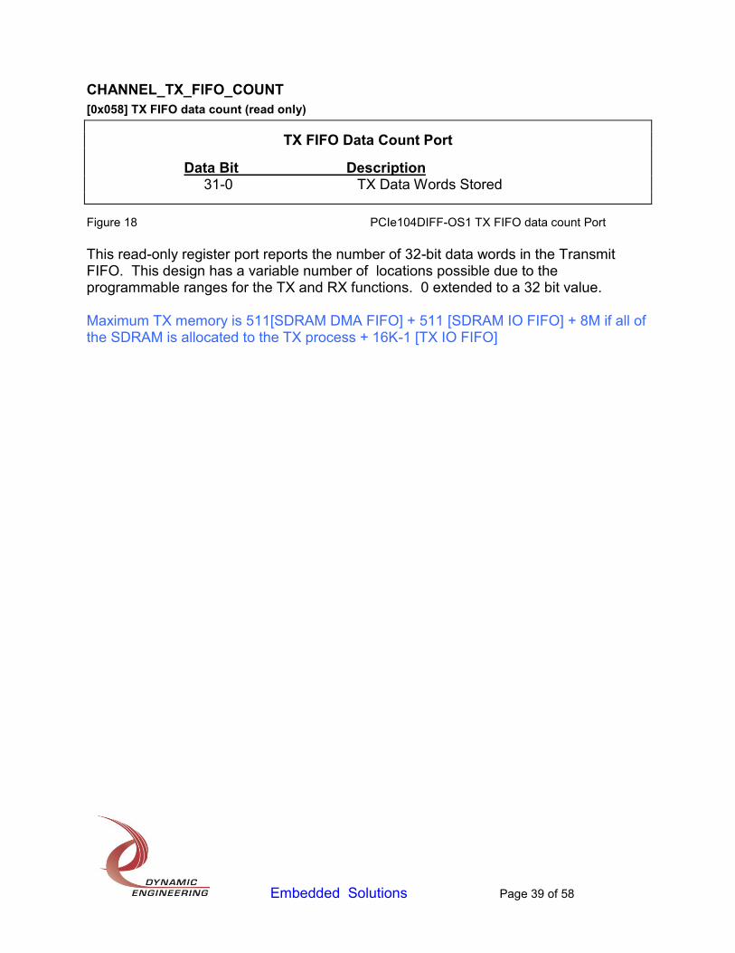
CHANNEL_WR_DMA_PNTR
[0x058] Write DMA Pointer (write only)
BurstIn DMA Pointer Address Register
Data Bit Description 31-2 First Chaining Descriptor Physical Address 1 direction [0] 0 end of chain
Figure 17 PCIe104DIFF-OS1 Write DMA pointer Register
This write-only port is used to initiate a scatter-gather write [TX] DMA. When the address of the first chaining descriptor is written to this port, the DMA engine reads three successive long words beginning at that address. Essentially this data acts like a chaining descriptor value pointing to the next value in the chain. The first is the address of the first memory block of the DMA buffer containing the data to read into the device, the second is the length in bytes of that block, and the third is the address of the next chaining descriptor in the list of buffer memory blocks. This process is continued until the end-of-chain bit in one of the next pointer values read indicates that it is the last chaining descriptor in the list. All three values are on LW boundaries and are LW in size. Addresses for successive parameters are incremented. The addresses are physical addresses the HW will use on the PCI bus to access the Host memory for the next descriptor or to read the data to be transmitted. In most OS you will need to convert from virtual to physical. The length parameter is a number of bytes, and must be on a LW divisible number of bytes. Status for the DMA activity can be found in the channel control register and channel status register. Notes:
1. Writing a zero to this port will abort a write DMA in progress. 2. End of chain should not be set for the address written to the DMA Pointer
Address Register. End of chain should be set when the descriptor follows the last length parameter.
3. The Direction should be set to ‘0’ for Burst In DMA in all chaining descriptor locations.
Embedded Solutions Page 39 of 58
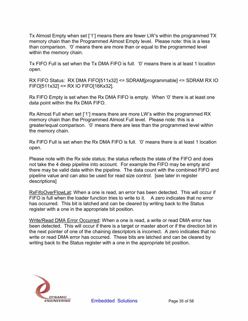
CHANNEL_TX_FIFO_COUNT
[0x058] TX FIFO data count (read only)
TX FIFO Data Count Port
Data Bit Description 31-0 TX Data Words Stored
Figure 18 PCIe104DIFF-OS1 TX FIFO data count Port
This read-only register port reports the number of 32-bit data words in the Transmit FIFO. This design has a variable number of locations possible due to the programmable ranges for the TX and RX functions. 0 extended to a 32 bit value. Maximum TX memory is 511[SDRAM DMA FIFO] + 511 [SDRAM IO FIFO] + 8M if all of the SDRAM is allocated to the TX process + 16K-1 [TX IO FIFO]
Embedded Solutions Page 40 of 58
CHANNEL_RD_DMA_PNTR
[0x05C] Read DMA Pointer (write only)
BurstIn DMA Pointer Address Register
Data Bit Description 31-2 First Chaining Descriptor Physical Address 1 direction [1] 0 end of chain
Figure 19 PCIe104DIFF-OS1 Read DMA pointer Register
This write-only port is used to initiate a scatter-gather read [RX] DMA. When the address of the first chaining descriptor is written to this port, the DMA engine reads three successive long words beginning at that address. Essentially this data acts like a chaining descriptor value pointing to the next value in the chain. The first is the address of the first memory block of the DMA buffer to write data from the device to, the second is the length in bytes of that block, and the third is the address of the next chaining descriptor in the list of buffer memory blocks. This process is continued until the end-of-chain bit in one of the next pointer values read indicates that it is the last chaining descriptor in the list. All three values are on LW boundaries and are LW in size. Addresses for successive parameters are incremented. The addresses are physical addresses the HW will use on the PCI bus to access the Host memory for the next descriptor or to read the data to be transmitted. In most OS you will need to convert from virtual to physical. The length parameter is a number of bytes, and must be on a LW divisible number of bytes. Status for the DMA activity can be found in the channel control register and channel status register. Notes:
1. Writing a zero to this port will abort a write DMA in progress. 2. End of chain should not be set for the address written to the DMA Pointer
Address Register. End of chain should be set when the descriptor follows the last length parameter.
3. The Direction should be set to ‘1’ for Burst Out DMA in all chaining descriptor locations.

Embedded Solutions Page 41 of 58
CHANNEL_RX_FIFO_COUNT
[0x05C] RX FIFO data count (read only)
RX FIFO Data Count Port
Data Bit Description 31-0 RX Data Words Stored
Figure 20 PCIe104DIFF-OS1 TX FIFO data count Port
This read-only register port reports the number of 32-bit data words in the Receive FIFO. This design has a variable number of locations possible due to the programmable ranges for the TX and RX functions. 0 extended to a 32 bit value. Maximum RX memory is 511[SDRAM DMA FIFO] + 511 [SDRAM IO FIFO] + 8M + DMA Pipeline if all of the SDRAM is allocated to the RX process + 16K-1[Rx IO FIFO] CHANNEL_FIFO_LW_Access
[0x060] Write TX/Read RX FIFO Port
RX and TX FIFO Port
Data Bit Description 31-0 FIFO data word
Figure 21 PCIe104DIFF-OS1 RX/TX FIFO Port
This port is used to make single-word accesses to and from the FIFO. Data read from this port will no longer be available for DMA transfers. Writing to the port loads the Tx FIFO, Reading unloads the Rx FIFO.
Embedded Solutions Page 42 of 58
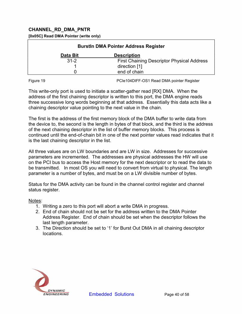
CHANNEL_TX_AMT_LVL
[0x064] Tx almost-empty level (read/write)
Tx Almost-Full Level Register
Data Bit Description 31-0 Tx FIFO Almost-Empty Level
Figure 22 PCIe104DIFF-OS1 TX ALMOST EMPTY LEVEL Register
This read/write port accesses the almost-empty level register. When the number of data words in the transmit data FIFO is less than than this value, the almost-empty status bit will be set. The register is R/W for 32 bits. The mask is valid for a size matching the depth of the FIFO. The count is based on the total memory allocated in the SDRAM memory chain.
CHANNEL_RX_AFL_LVL
[0x68] Rx almost-full (read/write)
Rx Almost-Full Level Register
Data Bit Description 31-0 Rx FIFO Almost-Full Level
Figure 23 PCIe104DIFF-OS1 RX ALMOST FULL LEVEL Register
This read/write port accesses the almost-full level register. When the number of data words in the receive data FIFO is equal or greater than this value, the almost-full status bit will be set. The register is R/W for 32 bits. The mask is valid for a size matching the depth of the FIFO. The count is based on the total memory allocated in the SDRAM memory chain. The level includes the pipeline for an additional 4 locations.
Embedded Solutions Page 43 of 58
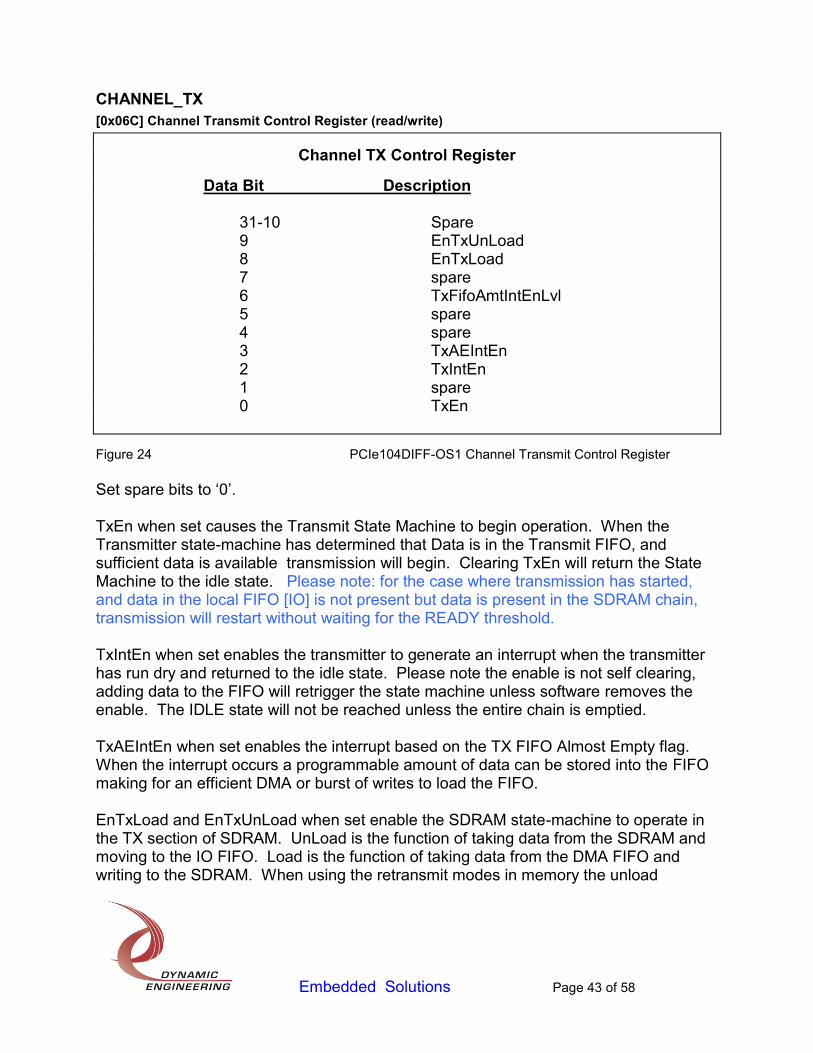
CHANNEL_TX
[0x06C] Channel Transmit Control Register (read/write)
Channel TX Control Register
Data Bit Description 31-10 Spare 9 EnTxUnLoad 8 EnTxLoad 7 spare 6 TxFifoAmtIntEnLvl 5 spare 4 spare 3 TxAEIntEn 2 TxIntEn 1 spare 0 TxEn
Figure 24 PCIe104DIFF-OS1 Channel Transmit Control Register
Set spare bits to ‘0’. TxEn when set causes the Transmit State Machine to begin operation. When the Transmitter state-machine has determined that Data is in the Transmit FIFO, and sufficient data is available transmission will begin. Clearing TxEn will return the State Machine to the idle state. Please note: for the case where transmission has started, and data in the local FIFO [IO] is not present but data is present in the SDRAM chain, transmission will restart without waiting for the READY threshold. TxIntEn when set enables the transmitter to generate an interrupt when the transmitter has run dry and returned to the idle state. Please note the enable is not self clearing, adding data to the FIFO will retrigger the state machine unless software removes the enable. The IDLE state will not be reached unless the entire chain is emptied. TxAEIntEn when set enables the interrupt based on the TX FIFO Almost Empty flag. When the interrupt occurs a programmable amount of data can be stored into the FIFO making for an efficient DMA or burst of writes to load the FIFO. EnTxLoad and EnTxUnLoad when set enable the SDRAM state-machine to operate in the TX section of SDRAM. UnLoad is the function of taking data from the SDRAM and moving to the IO FIFO. Load is the function of taking data from the DMA FIFO and writing to the SDRAM. When using the retransmit modes in memory the unload

Embedded Solutions Page 44 of 58
function can be left disabled until the pattern is loaded and then enabled. For FIFO mode both enables can be set together.
CHAN_TX_READY
[0x07C] Tx hold off (read/write)
Rx Almost-Full Level Register
Data Bit Description 31-0 Hold Off LW Count
Figure 25 PCIe104DIFF-OS1 TX Hold OFF Register
This read/write port is used to set a minimum threshold of data to be in the TX State-machine local FIFO before the State-Machine starts transmission. By programming this register to a non-zero amount the start and DMA start are decoupled somewhat. Setting the level to 100 LW, and the TX enabled before starting the DMA function will allow 100 LW to accumulate in the IO local buffer before enable is set and data is transmitted. This gives the DMA function a head start and will allow the data transfer to be done in one contiguous transfer. Your system may require larger or smaller settings. Only the TX IO FIFO is used to compare against the programmed count [ equal or greater] => the maximum is 16K-1. Do not set for more than the intended data size. Remember this is in LW; if you are thinking in bytes, divide by 4. If having the enable set and disabled a few times during start-up does not affect your application the count can be set to 0. During DMA start-up the system may break the first segments into small transfers causing the FIFO to only load 1 LW [4 bytes] several times before the DMA really gets going. This is an OS dependent phenomenon.
Embedded Solutions Page 45 of 58
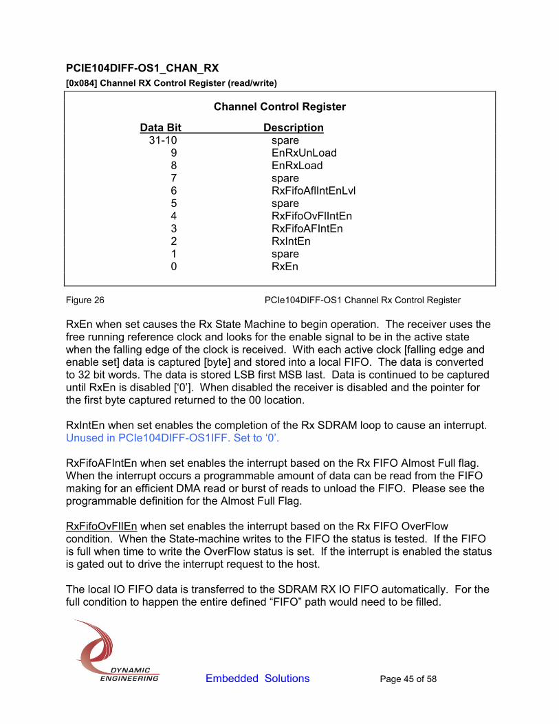
PCIE104DIFF-OS1_CHAN_RX
[0x084] Channel RX Control Register (read/write)
Channel Control Register
Data Bit Description 31-10 spare 9 EnRxUnLoad 8 EnRxLoad 7 spare 6 RxFifoAflIntEnLvl 5 spare 4 RxFifoOvFlIntEn 3 RxFifoAFIntEn 2 RxIntEn 1 spare 0 RxEn
Figure 26 PCIe104DIFF-OS1 Channel Rx Control Register
RxEn when set causes the Rx State Machine to begin operation. The receiver uses the free running reference clock and looks for the enable signal to be in the active state when the falling edge of the clock is received. With each active clock [falling edge and enable set] data is captured [byte] and stored into a local FIFO. The data is converted to 32 bit words. The data is stored LSB first MSB last. Data is continued to be captured until RxEn is disabled [‘0’]. When disabled the receiver is disabled and the pointer for the first byte captured returned to the 00 location. RxIntEn when set enables the completion of the Rx SDRAM loop to cause an interrupt. Unused in PCIe104DIFF-OS1IFF. Set to ‘0’. RxFifoAFIntEn when set enables the interrupt based on the Rx FIFO Almost Full flag. When the interrupt occurs a programmable amount of data can be read from the FIFO making for an efficient DMA read or burst of reads to unload the FIFO. Please see the programmable definition for the Almost Full Flag. RxFifoOvFlIEn when set enables the interrupt based on the Rx FIFO OverFlow condition. When the State-machine writes to the FIFO the status is tested. If the FIFO is full when time to write the OverFlow status is set. If the interrupt is enabled the status is gated out to drive the interrupt request to the host. The local IO FIFO data is transferred to the SDRAM RX IO FIFO automatically. For the full condition to happen the entire defined “FIFO” path would need to be filled.

Embedded Solutions Page 46 of 58
EnRxLoad and EnRxUnLoad when set enable the SDRAM state-machine to operate in the RX section of SDRAM. UnLoad is the function of taking data from the SDRAM and moving to the DMA FIFO. Load is the function of taking data from the IO FIFO and writing to the SDRAM. When using the retransmit modes in memory the unload function can be left disabled until the pattern is loaded and then enabled. For FIFO mode both enables can be set together. While it is unlikely that the RX retransmit function would be used, it can be used as a self generating data stream for testing system operation. Due to schedule requirements this function has not been tested for PCIe104DIFF-OS1.
Memory & Loopback Registers
[0x0A0 – 0x0EF ] Memory & Loopback
Memory and loopback registers are not supported for this design.
Channel1 Registers
[0x0F0 – 0x18F ] Channel1
Channel1 registers are reserved for test only in this design

Embedded Solutions Page 47 of 58
Board Features
DIP Switches There is one DIP Switch with 8 switches on the PCIe104DIFF-OS1. It is labeled SW1 with bit numbers 7 to 0 and ‘1’ ‘0’ for on/off in the silk screen.
SW1 is for user purposes. The settings of SW1 can be seen/used by reading the Switch_Revision_ID register [7:0] bits which correspond to SW1 [7:0] bit positions/ The default setting of all SW1 switches after manufacturing is off/’0’. Differential Transmitter/Receivers To be added in the next revision PLL The Cypress 22393 PLL is handy for creating user specific frequencies with which to operate the state-machines and I/O. The driver supports programming the PLL over a serial I²C bus. Two clocks are received from the PLL into the FPGA - see figure below. The clock routing uses matched lengths to provide in-phase references should they be necessary in your design. The FPGA clock features provide further clock functionality. PCIe104DIFF-OS1 uses the on-board oscillator (50 MHz) as the reference for the PCIe104DIFF-OS1.jed can be used to set this frequency. Cypress has a utility available for calculating the frequency control words for the PLL. http://www.dyneng.com/CyberClocks.zip is the URL for the Cypress software used to calculate the PLL programming words. The PLL responds to one of two device ids (only one works). As part of our ATP our software determines the address of the PLL. The software is part of the engineering kit and can be ported to your application.
PLL Schematic Figure goes here
Embedded Solutions Page 48 of 58
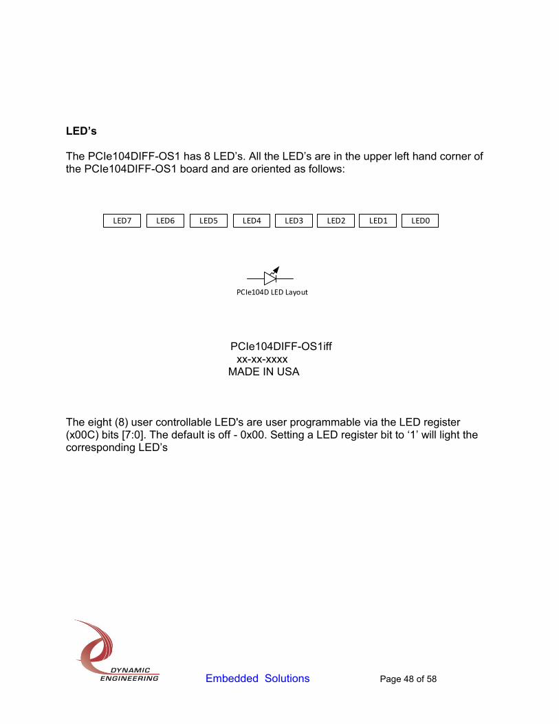
LED’s The PCIe104DIFF-OS1 has 8 LED’s. All the LED’s are in the upper left hand corner of the PCIe104DIFF-OS1 board and are oriented as follows:
PCIe104D LED Layout
LED0LED1LED2LED3LED4LED5LED6LED7
PCIe104DIFF-OS1iff xx-xx-xxxx MADE IN USA The eight (8) user controllable LED's are user programmable via the LED register (x00C) bits [7:0]. The default is off - 0x00. Setting a LED register bit to ‘1’ will light the corresponding LED’s

Embedded Solutions Page 49 of 58
Product Adaptability
A wide range of interfaces and protocols can be implemented with the PCIe104DIFF-OS1; UART, Manchester encoding, serial or parallel, LVDS, ECL/NECL and/or TTL. The interfaces can be created using the hardware and development tools provided with the PCIe104DIFF-OS1 along with the Lattice software. Once your requirements are known the design can be implemented in RTL and compiled with the Lattice design software. The output file can then be programmed into the Lattice Flash on the PCIe104DIFF-OS1. Because the FLASH is reprogrammable, the design can be implemented in phases. Experiment and test out concepts and partial implementations during the design phase or perhaps simulate other hardware that needs to be implemented. As an example consider a parallel interface with 4 data lines, 4 control signals and a clock for each direction. The PCIe104DIFF-OS1 has 18 differential I/O, so there is enough I/O for a full duplex implementation. The parallel channel(s) would be supported with the 8Mx16 external FIFO and internal FIFO’s that were instantiated out of block RAM. The FPGA is a Lattice ECP3 industrial temp part in the –8 speed grade. The PCIe interface and SDRAM controller occupy approximately 50% of the device so there is of room for more complex data formatting requirements. For systems with an external reference clock dedicated FPGA clock inputs can be used for long line pins or they can be routed through a Digital Clock Manager to create a low skew clock distribution based on an external reference.

Embedded Solutions Page 50 of 58
PCIe104DIFF-OS1 Interrupts – Appendix A
Please see individual Interrupt register bits for descriptions and usage of PCIe104 Interrupts. This section is provided to summarize the PCIe104DIFF-OS1 Interrupts, Interrupt registers, programmable features usage, and behavior. Here’s a brief description of what’s covered:
o Summary of PCIe spec. Interrupt configuration registers o Summary of Interrupt registers/bits contained in the PCIe104DIFF-OS1. o Summary of the PCIe104DIFF-OS1’s Interrupt specific registers and bits. o Detailed description of PCIe104DIFF-OS1’s Interrupt functionality and features. o Detailed summary of the PCIe104DIFF-OS1’s Interrupt specific registers and
bits. PCIe104DIFF-OS1 PCI Express Interrupt Registers Summary PCI Express has two possible types of Interrupt packets that can be generated, they are:
INTx# – Legacy PCI Interrupt virtualization packets.
MSI – Message Signal Interrupt packets. PCIe104DIFF-OS1 supports both MSI and INTx# interrupt packet generation. There are eight PCI Express configuration (type 0) registers contained in the PCIe104DIFF-OS1 which are involved in the generation of interrupt packets. The next section summarizes the four registers with INTx# related bits, followed by a section that summarizes the four registers with MSI related bits. The summary of these registers is provided to ease users understanding of PCI Express Interrupts. Users need not be concerned with setting or using the register values written by the host as they are used by the PCIe104DIFF-OS1 PCI Express core when generating INTx# or MSI PCI Express packets.

Embedded Solutions Page 51 of 58
PCIe104DIFF-OS1 PCI Express INTx# Interrupt Configuration Registers Summary Command Register (offset 0x04)
Interrupt Disable (bit [10]) R/W, 0 = INTx# enabled (default), 1 = INTx# disabled. Status Register (offset 0x06)
Interrupt Status (bit [3]) RO, 0 = no Interrupt pending (default), 1 = Interrupt pending. Only valid in INTx# Mode. Disabled, always zero in MSI mode.
Capabilities List (bit [4]) RO, 0 no capabilities registers, 1 = capabilities registers exist. This bit is hardwired to 1 in PCIe104DIFF-OS1 - MSI registers are capability registers.
Interrupt Line Register (offset 0x3C)
Interrupt Line [7:0] R/W register written by the Host to distinguish device interrupt.
Interrupt Pin Register (offset 0x3D)
Interrupt Pin [7:0] RO register, hardwired to 0x01 in PCIe104DIFF-OS1 to indicate INTA#.
PCIe104DIFF-OS1 PCI Express MSI Interrupt Configuration Registers Summary Message Control Register (offset 0x72)
MSI Enable (bit [0]) R/W, 0 = MSI’s disabled (default), 1 = MSI’s enabled.
Multiple Message Capable (bits [3:1]) RO, 0x0 = PCIe104DIFF-OS1 requests 1 MSI.
Multiple Message Enable (bits [6:4]) R/W, 0x0 (default) Host writes to allocate MSI’s.
64 bit Address Capable (bit [7]) RO, 1 = PCIe104DIFF-OS1 is 64 bit MSI address capable.
Message Address Register (offset 0x74)
Message Address (bits [31:2]) R/W, Host provides - bits [31:2] of D-Word aligned MSI address.
Message Upper Address Register (offset 0x78)
Message Address (bits [63:32]) R/W, Host provides - upper 32bits for 64bit MSI addressing.
Message Data Register (offset 0x7C)
Message Data (bits [15:0]) R/W, Host provides - value used to distinguish PCIe104DIFF-OS1 interrupt.

Embedded Solutions Page 52 of 58
PCIe104DIFF-OS1 Interrupts and Registers Summary For each channel there are four possible interrupt sources. PCIe104DIFF-OS1 Interrupt Functional Operation The descriptions of the PCIe104DIFF-OS1 interrupt behavior to follow refer to the PCIe compliant configuration registers and PCIe104DIFF-OS1 specific Interrupt registers both of which were summarized in sections 1.0 and 2.0. This was done for the convenience of the reader and should be sufficient for understanding the remainder of this document. When PCIe104DIFF-OS1 comes out of reset it is in INTA# mode as both the Interrupt Disable and MSI Enable bits are 0 by default. It is up to the Host to determine if all devices in the system can support MSI before configuring the system to use MSI Interrupts. This section will first describe how PCIe104DIFF-OS1 INTA# virtualized signaling works then describe the setup, functional, and behavioral differences for MSI Interrupts. PCIe104DIFF-OS1 INTA# Interrupt Functional Operation To be added next revision PCIe104DIFF-OS1 Interrupt Functionality To be added next revision PCIe104DIFF-OS1 Interrupt Timing, Behavior, and W1C To be added next revision PCIe104DIFF-OS1 MSI Interrupts Per the PCI Express specification, when a PCI Express device supports both virtualized INTx messages and MSI, only one of the mechanism will be enabled at any given time. When PCIe104DIFF-OS1 comes out of reset it is in INTA# mode as both the Interrupt Disable and MSI Enable bits are 0 by default. Also per spec, setting the MSI Enable bit in the Message Control Register (offset 0x72) disables the PCIe104DIFF-OS1 ability to use INTx messages and enables MSI. Before enabling MSI the Host needs to write valid values in the Message Address and Message Data registers. It should also leave the Multiple Message Enable field at the

Embedded Solutions Page 53 of 58
default value of 0x0h as PCIe104DIFF-OS1 only requests and indicates support for one MSI via the Multiple Message Capable bits = 0x0h. See section 2.0 for a complete summary of MSI registers/bits. Once enabled, the key difference between PCIe104DIFF-OS1’s MSI and INTA# interrupt generation is that only one MSI packet will be sent to the Host to indicate an Interrupt assertion. No MSI packet is generated or sent when the ISR interrupt bit or bits are cleared using a W1C. The timing of when an MSI packet is sent in response to an assertion is identical to when an INTA# assert packet is sent as described in previous sections. When PCIe104DIFF-OS1 generates and sends the MSI packet it uses the Message Address and Data register values provided by the Host to create the MSI (Memory Write) packet. PCIe104DIFF-OS1 Important Interrupt Notes To be added next revision
Mechanical
Mechanical section to be available upon next release.
Applications Guide
Applications Guide section to be available upon next release.
Electrical
Electrical section to be available upon next release.

Embedded Solutions Page 54 of 58
AC/DC Timing
AC/DC Timing section to be available upon next release.
Interfacing
Some general interfacing guidelines are presented below. Do not hesitate to contact the factory if you need more assistance. ESD Proper ESD handling procedures must be followed when handling the PCIe104DIFF-OS1. The card is shipped in an anti-static, shielded bag. The card should remain in the bag until ready for use. When installing the card the installer must be properly grounded and the hardware should be on an anti-static work-station. Start-up Make sure that the "system" can see your hardware before trying to access it. Many BIOS will display the PCI Express devices found at boot up on a "splash screen" with the VendorID and CardId and an interrupt level. Look quickly! If the information is not available from the BIOS then a third party PCI device cataloging tool will be helpful. In Windows systems the device manager can be used. Watch the system grounds. All electrically connected equipment should have a fail-safe common ground that is large enough to handle all current loads without affecting noise immunity. Power supplies and power consuming loads should all have their own ground wires back to a common point.

Embedded Solutions Page 55 of 58
Construction and Reliability
PCIe Modules while commercial in nature can be conceived and engineered for rugged industrial environments. PCIe104DIFF-OS1 is constructed out of 0.062 inch thick High Temp FR4 material. Surface mount components are used. Most devices are high pin count compared to mass of the device. For high vibration environments inductors and other higher mass per joint components can be glued down. Conformal Coating is an option. For condensing environments conformal coating is required. ROHS processing is an option. Standard lead solder is used unless “-ROHS” is added to the part number.
Thermal Considerations
The PCIe104DIFF-OS1 design consists of CMOS circuits. The power dissipation due to internal circuitry is very low. With the one degree differential temperature to the solder side of the board external cooling is easily accomplished.

Embedded Solutions Page 56 of 58
Warranty and Repair
Please refer to the warranty page on our website for the current warranty offered and options. http://www.dyneng.com/warranty.html
Service Policy
Before returning a product for repair, verify as well as possible that the suspected unit is at fault. Then call the Customer Service Department for a RETURN MATERIAL AUTHORIZATION (RMA) number. Carefully package the unit, in the original shipping carton if this is available, and ship prepaid and insured with the RMA number clearly written on the outside of the package. Include a return address and the telephone number of a technical contact. For out-of-warranty repairs, a purchase order for repair charges must accompany the return. Dynamic Engineering will not be responsible for damages due to improper packaging of returned items. For service on Dynamic Engineering Products not purchased directly from Dynamic Engineering contact your reseller. Products returned to Dynamic Engineering for repair by other than the original customer will be treated as out-of-warranty.
Out of Warranty Repairs
Out of warranty repairs will be billed on a material and labor basis. Customer approval will be obtained before repairing any item if the repair charges will exceed one half of the quantity one list price for that unit. Return transportation and insurance will be billed as part of the repair and is in addition to the minimum charge.
For Service Contact:
Customer Service Department Dynamic Engineering 150 DuBois, Suite C Santa Cruz, CA 95060 (831) 457-8891 - Fax (831) 457-4793 [email protected]

Embedded Solutions Page 57 of 58
Specifications
PCIe Interfaces: PCIe 1 lane (x1) interface
Access types: Configuration and Memory space utilized
CLK rates supported: Standard 100 MHz PCI Express differential reference clock for PCIe interface. Diff interface clock rates up to 150MHz
Memory Multiple FIFO’s are implemented to support multiple parallel processes at any one time within the Lattice FPGA’s. Parallel processing is achieved with Tx and Rx channel operating in parallel.
IO CMOS Drivers/Receivers to/from Differential Drivers/Receivers.
Interface: DB37 male with 4-40 posts. Standard single connector PCIe104 stacking connector.
Software Interface: Control Registers within Lattice FPGA. Drivers provide generic calls for GPB access to allow any user modification to be programmed with the standard driver.
Initialization: Programming procedure documented in this manual
Access Modes: DMA and standard target read and write to registers and memory.
Access Time: PCIe Core time-out.
Interrupt: Multiple interrupt sources. The interrupts are maskable and are supported with a status and control registers.
Onboard Options: Board Stuffing Options: Dimensions:
Construction: High Temp FR4 Multi-Layer Printed Circuit, Surface Mount Components.
Power:
User 8 position software readable switch
8 software controllable LED's

Embedded Solutions Page 58 of 58
Order Information
Standard temperature range -40-85øC
PCIe104DIFF-OS1-OS1 http://www.dyneng.com/PCIe104Diff.html INT and MSI interrupt options, OS1 interface : LVDS, Clk, Data, STB, Inhibit full duplex.
-ROHS Change to ROHS processing. Otherwise leaded solder is used.
-CC Add Conformal Coating for condensing environments
Drivers/Reference Software Clients of PCIe104DIFF-OS1 have access to existing drivers and reference software packages.
All information provided is Copyright Dynamic Engineering