Embed Size (px)
Citation preview

1 IntroductionWith the computation power of Freescale digital signalcontrollers (DSCs) and the flexibility of their peripherals, therequirements for the applications grow up. One of suchrequirements is to drive two permanent magnet synchronousmotors (PMSM) in field-oriented control (FOC) on a singleprocessor.
Dual PMSM FOC on a single processor brings morecomplexity to the application, mainly in terms of the PWMmodules of synchronization of both the motors, the ADCsynchronization to both the PWM modules including a rightpoint to trigger the ADC, and finally, the time when the fastand slow control loops of both the motors are calculated.
This application note guides:• to set up and synchronize both the PWM modules• how and where to generate trigger signals for the ADC
module from the PWM module• when to call the fast and slow loop calculation of FOC
algorithm of both the motors
Freescale Semiconductor Document Number:AN4608
Application Note Rev. 0, 10/2012
Use of PWM and ADC onMC56F84789 to Drive Dual PMSMotor FOCby: Jaroslav Musil
© 2012 Freescale Semiconductor, Inc.
Contents
1 Introduction............................................................1
2 Digital signal controller (DSC)...............................2
3 Steps in configuration flow ....................................2
4 PWM configuration.................................................3
5 PWM A and PWM B synchronization....................6
6 PWM triggers for ADC...........................................9
7 ADC configuration................................................11
8 PWM and ADC signalsinterconnection.....................................................13
9 Triggers startup sequence.....................................15
10 Reading ADC samples..........................................16
11 Complete code.......................................................19
12 Definitions and acronyms.....................................24

2 Digital signal controller (DSC)One of suitable DSCs for dual motor control application is MC56F84789. This controller has the following features theapplication can benefit from:
• 100 MHz core and peripheral clock• Two 4-channel PWM modules with a possibility of multiple triggers• High-speed 12-bit ADC with a possibility to sample two signals simultaneously• Two crossbar units to interconnect signals between the peripherals• And-Or-Invert to logically mix the signals among the peripherals• Interrupt controller with priorities
The processor has much more modules but for this application note, only the above-mentioned ones will be discussed.
Figure 1 shows how the processor signals are connected to the power electronics on the board.
Figure 1. Processor connection to the board circuitry
3 Steps in configuration flowIn order to configure the DSC properly, follow the steps given below:
• PWM configuration: It configures the PWM A and B modules to generate signals to drive the motors.• PWM A and B synchronization: It synchronizes the PWM A and B signals to be in phase shift of 90 degrees.• PWM triggers for ADC: It sets up the points where the ADC will be triggered to sample the signals.
Digital signal controller (DSC)
Use of PWM and ADC on MC56F84789 to Drive Dual PMS Motor FOC, Rev. 0, 10/2012
2 Freescale Semiconductor, Inc.
• ADC configuration: It configures the ADC modules to sample the desired signals.• PWM and ADC signal interconnection: It configures the crossbar switches and the AOI module to lead the PWM
triggered toward the ADC synchronization input.• Triggers startup sequence: It enables the triggers in the correct sequence to be aligned with the ADC channels
sequence.• Reading ADC samples: It sets up the interrupts to read the sampled values and call the algorithms.
All the above-mentioned steps are mentioned in detail, in the forthcoming sections.
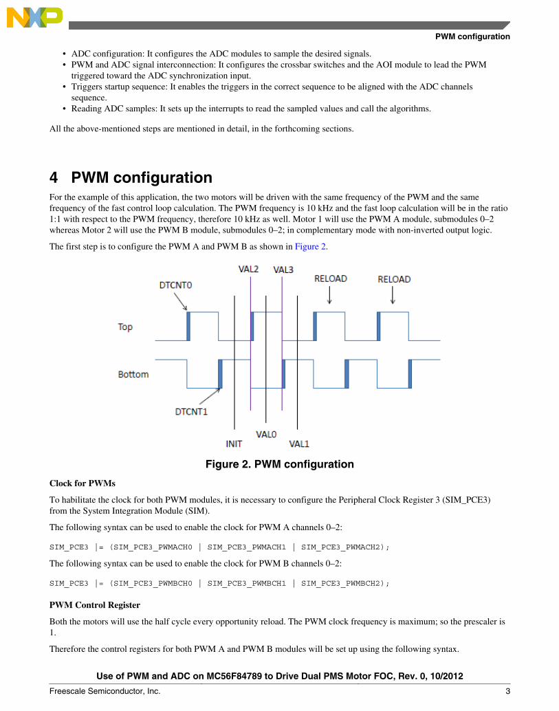
4 PWM configurationFor the example of this application, the two motors will be driven with the same frequency of the PWM and the samefrequency of the fast control loop calculation. The PWM frequency is 10 kHz and the fast loop calculation will be in the ratio1:1 with respect to the PWM frequency, therefore 10 kHz as well. Motor 1 will use the PWM A module, submodules 0–2whereas Motor 2 will use the PWM B module, submodules 0–2; in complementary mode with non-inverted output logic.
The first step is to configure the PWM A and PWM B as shown in Figure 2.
Figure 2. PWM configuration
Clock for PWMs
To habilitate the clock for both PWM modules, it is necessary to configure the Peripheral Clock Register 3 (SIM_PCE3)from the System Integration Module (SIM).
The following syntax can be used to enable the clock for PWM A channels 0–2:
SIM_PCE3 |= (SIM_PCE3_PWMACH0 | SIM_PCE3_PWMACH1 | SIM_PCE3_PWMACH2);
The following syntax can be used to enable the clock for PWM B channels 0–2:
SIM_PCE3 |= (SIM_PCE3_PWMBCH0 | SIM_PCE3_PWMBCH1 | SIM_PCE3_PWMBCH2);
PWM Control Register
Both the motors will use the half cycle every opportunity reload. The PWM clock frequency is maximum; so the prescaler is1.
Therefore the control registers for both PWM A and PWM B modules will be set up using the following syntax.
PWM configuration
Use of PWM and ADC on MC56F84789 to Drive Dual PMS Motor FOC, Rev. 0, 10/2012
Freescale Semiconductor, Inc. 3

Motor 1:
PWMA_SM0CTRL = PWMA_SM0CTRL_HALF; PWMA_SM1CTRL = PWMA_SM1CTRL_HALF; PWMA_SM2CTRL = PWMA_SM2CTRL_HALF;
Motor 2:
PWMB_SM0CTRL = PWMB_SM0CTRL_HALF; PWMB_SM1CTRL = PWMB_SM1CTRL_HALF; PWMB_SM2CTRL = PWMB_SM2CTRL_HALF;
PWM Control 2 Register
The setup of the co-operation of the submodules requires PWM Control 2 Register to be properly set up.1. Enable the PWM in the debug and wait mode, force initialization for the channels 02. For the channels 1 and 2, set the additional bits:
• initialization from the master sync from submodule 0• master reload signal to force the update• master reload from submodule 0 to reload value registers• submodule 0 clock to be used as the clock source
The control registers for both the modules can be configured using the following syntax.
Motor 1:
PWMA_SM0CTRL2 = 0xC080;PWMA_SM1CTRL2 = 0xC20E; PWMA_SM2CTRL2 = 0xC20E;
Motor 2:
PWMB_SM0CTRL2 = 0xC080; PWMB_SM1CTRL2 = 0xC20E; PWMB_SM2CTRL2 = 0xC20E;
PWM modulo setup
The PWM modulo to generate 10 kHz is derived from the 100 MHz clock. Thus, the modulo is 100 MHz / 10 kHz = 10,000ticks. The PWM modules have the INIT register value where the counter starts and VAL1 register value where the counter isreinitialized. So, the INIT value will be set up to negative value of the half modulo, and the VAL1 value will be set up topositive value of the half modulo–1. The reload is in the half cycle, that is, in the middle of these two values. To sum it up:
INIT =–5000 (0xEC78), VAL1 = 4999 (0x1387), VAL0 = 0. The following syntax can be used to configure it.
Motor 1:
PWMA_SM0INIT = 0xEC78;PWMA_SM1INIT = 0xEC78;PWMA_SM2INIT = 0xEC78;
PWMA_SM0VAL1 = 0x1387; PWMA_SM1VAL1 = 0x1387; PWMA_SM2VAL1 = 0x1387;
PWMA_SM0VAL0 = 0x0000; PWMA_SM1VAL0 = 0x0000;PWMA_SM2VAL0 = 0x0000;
Motor 2:
PWMB_SM0INIT = 0xEC78;PWMB_SM1INIT = 0xEC78;PWMB_SM2INIT = 0xEC78;
PWMB_SM0VAL1 = 0x1387; PWMB_SM1VAL1 = 0x1387;
PWM configuration
Use of PWM and ADC on MC56F84789 to Drive Dual PMS Motor FOC, Rev. 0, 10/2012
4 Freescale Semiconductor, Inc.

PWMB_SM2VAL1 = 0x1387;
PWMB_SM0VAL0 = 0x0000; PWMB_SM1VAL0 = 0x0000; PWMB_SM2VAL0 = 0x0000;
50% duty cycle initialization
To initialize the module with the 50% duty cycle, it is necessary to set up the VAL2 and VAL3 registers. As it is theComplementary mode, the VAL4 and VAL5 registers are not used for the PWM edges generation. VAL2 is loaded with anegative value of the half modulo divided by 2; VAL3 is loaded with the positive value of the half modulo divided by 2.
Therefore VAL2 =–2500 (0xF63CU), VAL3 = 2500 (0x09C3). The following syntax can be used to configure it.
Motor 1:
PWMA_SM0VAL2 = 0xF63C; PWMA_SM1VAL2 = 0xF63C; PWMA_SM2VAL2 = 0xF63C;
PWMA_SM0VAL3 = 0x09C3; PWMA_SM1VAL3 = 0x09C3; PWMA_SM2VAL3 = 0x09C3;
Motor 2:
PWMB_SM0VAL2 = 0xF63C; PWMB_SM1VAL2 = 0xF63C; PWMB_SM2VAL2 = 0xF63C;
PWMB_SM0VAL3 = 0x09C3; PWMB_SM1VAL3 = 0x09C3; PWMB_SM2VAL3 = 0x09C3;
2 µs deadtime
To set up the deadtime, configure the DTCNT0 (top switch) and DTCNT1 (bottom switch) register values. The value isderived from the module clock, therefore for 2 µs, the value will be 100 MHz x 2 µs = 200 (0x00C8). The following codeconfigures the deadtime:
Motor 1:
PWMA_SM0DTCNT0 = 0x00C8; PWMA_SM1DTCNT0 = 0x00C8; PWMA_SM2DTCNT0 = 0x00C8;
PWMA_SM0DTCNT1 = 0x00C8; PWMA_SM1DTCNT1 = 0x00C8; PWMA_SM2DTCNT1 = 0x00C8;
Motor 2:
PWMB_SM0DTCNT0 = 0x00C8; PWMB_SM1DTCNT0 = 0x00C8; PWMB_SM2DTCNT0 = 0x00C8;
PWMB_SM0DTCNT1 = 0x00C8; PWMB_SM1DTCNT1 = 0x00C8; PWMB_SM2DTCNT1 = 0x00C8;
Disable faults
This example will not use the fault logic, so it is necessary to disable the fault mapping registers using the following syntax.
Motor 1:
PWMA_SM0DISMAP0 = 0;PWMA_SM1DISMAP0 = 0;PWMA_SM2DISMAP0 = 0;
PWM configuration
Use of PWM and ADC on MC56F84789 to Drive Dual PMS Motor FOC, Rev. 0, 10/2012
Freescale Semiconductor, Inc. 5

PWMA_SM0DISMAP1 = 0; PWMA_SM1DISMAP1 = 0; PWMA_SM2DISMAP1 = 0;
Motor 2:
PWMB_SM0DISMAP0 = 0; PWMB_SM1DISMAP0 = 0; PWMB_SM2DISMAP0 = 0;
PWMB_SM0DISMAP1 = 0; PWMB_SM1DISMAP1 = 0; PWMB_SM2DISMAP1 = 0;
LDOK bit
The final step before running PWM is to clear and set MCTRL[LDOK] using the following code.
Motor 1:
PWMA_MCTRL |= PWMA_MCTRL_CLDOK_0 | PWMA_MCTRL_CLDOK_1 | PWMA_MCTRL_CLDOK_2;PWMA_MCTRL |= PWMA_MCTRL_LDOK_0 | PWMA_MCTRL_LDOK_1 | PWMA_MCTRL_LDOK_2;
Motor 2:
PWMB_MCTRL |= PWMB_MCTRL_CLDOK_0 | PWMB_MCTRL_CLDOK_1 | PWMB_MCTRL_CLDOK_2;PWMB_MCTRL |= PWMB_MCTRL_LDOK_0 | PWMB_MCTRL_LDOK_1 | PWMB_MCTRL_LDOK_2;
The PWM A and PWM B are configured to generate a signal as shown in Figure 1. But to get their signals out on the pins,the GPIO pins must be properly configured. So, certain GPIO E and GPIO G pins must be set up as peripherals. In case ofmultiple peripheral options, the PWM option must be chosen. The GPIO E and GPIO G clocks must be also enabled. Thecode is the following:
/* Enable GPIOE clock */SIM_PCE0 |= SIM_PCE0_GPIOE;
/* PWMA PWMB */ GPIOE_PER |= (GPIOE_PER_PE_0 | GPIOE_PER_PE_1 | GPIOE_PER_PE_2 | GPIOE_PER_PE_3 | GPIOE_PER_PE_4 | GPIOE_PER_PE_5 | GPIOE_PER_PE_8 | GPIOE_PER_PE_9); SIM_GPSEL &= ~(SIM_GPSEL_E4 | SIM_GPSEL_E5);SIM_GPSEH &= ~(SIM_GPSEH_E8 | SIM_GPSEH_E9);
/* Enable GPIOG clock */SIM_PCE0 |= SIM_PCE0_GPIOG;
/* PWM B */GPIOG_PER |= (GPIOG_PER_PE_0 | GPIOG_PER_PE_1 | GPIOG_PER_PE_2 | GPIOG_PER_PE_3);SIM_GPSGL &= ~(SIM_GPSGL_G0 | SIM_GPSGL_G1 | SIM_GPSGL_G2 | SIM_GPSGL_G3);
Finally, the only missing items are to send the run command to the modules to start generation of the signal and to enable thePWM signals out on the pins. The PWM modules must not be started at this time because it is needed to synchronize both thePWMs.
5 PWM A and PWM B synchronizationThe PWM A and PWM B have been configured; they haven’t been started yet. So the next step is to synchronize the PWMmodules somehow.
PWM A and PWM B synchronization
Use of PWM and ADC on MC56F84789 to Drive Dual PMS Motor FOC, Rev. 0, 10/2012
6 Freescale Semiconductor, Inc.

To calculate the fast loop algorithm in each PWM cycle, it is necessary to shift the PWM signals to each other because it isimpossible to calculate the algorithms of two motors at the same time. Therefore, the PWM signals must be shifted. Toeffectively distribute the energy from the DC bus capacitor, it is recommended to avoid simultaneous switching; that is, to beshifted by 180 degrees. As the MC56F84789 processor has good computation power to calculate the FOC algorithm quicklyand effectively, the signals will be shifted by 90 degrees to have an optimum.
The desired signals from both PWM modules are shown in Figure 3.
PWM 90-degree shift principle
As shown in Figure 3, the PWM B INIT value lags by 90 degrees with respect to the PWM A INIT value. This shift is equalto the modulo divided by 4. When the PWM RUN signal is applied, the PWM module starts counting up from the INITvalue, which is beneficial for this application.
The process to synchronize the PWM modules includes:• starting the PWM A module• generating an interrupt at the modulo / 4 instant from the PWM A module• starting the PWM B module from the generated PWM A module interrupt• disabling the further interrupt for this PWM A module event
Modulo / 4 event configuration
Before starting the PWM A module, the interrupt on the module / 4 event must be programmed. To generate such an event,the unused VAL5 value will be used. It does not matter which submodule will generate this event. In this example, thesubmodule 1 VAL5 value will be used.
So in the code, the submodule 1 VAL5 is to be programmed with the modulo / 4 value, which is –2500 (0xF63C); thecompare interrupt of this submodule is to be enabled and the interrupt controller has to be programmed to enable thisinterrupt.
The code lines are the following:
/* Sync for the other motor's PWM */PWMA_SM1VAL5 = 0xF63C;/* Compare interrupt of Value 5, used at init to sync PWM A and PWM B */PWMA_SM1INTEN = PWMA_SM1INTEN_CMPIE_5;/* Interrupt for the SM1 CMP Level 2 */INTC_IPR9 |= INTC_IPR9_PWMA_CMP1;
PWM A and PWM B synchronization
Use of PWM and ADC on MC56F84789 to Drive Dual PMS Motor FOC, Rev. 0, 10/2012
Freescale Semiconductor, Inc. 7

Figure 3. PWM A and PWM B synchronization
VAL5 Compare interrupt service routine
The PWM submodule 1 VAL5 Compare interrupt has been configured. Now the interrupt service routine (ISR) must becreated to start the PWM B module.
The name of the ISR will be IsrPWMSync. A prototype for this routine must be created in the prototype section of the code:
void IsrPWMSync(void);
The name of this function must be copied into the vector table; in case the default CodeWarrior 10.2 project template is used,it is in the file MC56F847xx_vector.asm (located in Project_Settings\Startup_Code). Thus at the address 0xAA, the interruptno. 85 for the PWM A submodule 1 will contain the following statement:
JSR >FIsrPWMSync
The body of the function itself contains the following actions:• if condition, if the source is the VAL5 Compare• RUN command application on the PWM B module• disabling the VAL5 Compare interrupt• clearing the VAL5 Compare flag
So putting all this into the code will look like this:
#pragma interrupt alignspvoid IsrPWMSync(void){ if ((PWMA_SM1STS & PWMA_SM1STS_CMPF_5) > 0 ) { /* Starts PWM B */ PWMB_MCTRL |= PWMB_MCTRL_RUN_0 | PWMB_MCTRL_RUN_1 | PWMB_MCTRL_RUN_2;
/* Disable PWM SM1 CMP interrupt from 5 */ PWMA_SM1INTEN &= ~PWMA_SM1INTEN_CMPIE_5;
PWM A and PWM B synchronization
Use of PWM and ADC on MC56F84789 to Drive Dual PMS Motor FOC, Rev. 0, 10/2012
8 Freescale Semiconductor, Inc.

/* Clears compare flag */ PWMA_SM1STS |= PWMA_SM1STS_CMPF_5; }}
PWM A start
The PWM A and B channels have been configured, the synchronization event has been set up, and the interrupt serviceroutine is written. So now, the only action is to apply the RUN command on the PWM A and enable the PWM A and PWMB signals out to the pins. When the PWM A is started, it will generate the programmed submodule 1 VAL5 Compareinterrupt where the PWM B will be started and this interrupt, blocked.
The code to start the PWM A is the following (this command is to be called after the PWM A and PWM B modulesconfiguration and after the Compare interrupt is set up):
PWMA_MCTRL |= PWMA_MCTRL_RUN_0 | PWMA_MCTRL_RUN_1 | PWMA_MCTRL_RUN_2;
The command to enable the PWM A and PWM B singals out to the pins will look like this:
PWMA_OUTEN |= (PWMA_OUTEN_PWMA_EN_0 | PWMA_OUTEN_PWMB_EN_0 | PWMA_OUTEN_PWMA_EN_1 | PWMA_OUTEN_PWMB_EN_1 | PWMA_OUTEN_PWMA_EN_2 | PWMA_OUTEN_PWMB_EN_2);
PWMB_OUTEN |= (PWMB_OUTEN_PWMA_EN_3 | PWMB_OUTEN_PWMB_EN_3 | PWMB_OUTEN_PWMA_EN_1 | PWMB_OUTEN_PWMB_EN_1 | PWMB_OUTEN_PWMA_EN_2 | PWMB_OUTEN_PWMB_EN_2);
Figure 3 shows the signals on the pins, that should be also observed on the scope.
6 PWM triggers for ADCThe FOC of PMSM requires analog signals which are used in the control algorithm to be measured. The required quantitiesfor such control are the motor phase currents and the DC bus voltage.
Typically the currents are measured on shunt resistors connected below the bottom MOSFET’s (or IGBT’s). See Figure 4. Inthis constellation, the motor current is only visible when the particular bottom MOSFET is turned on. Therefore the ADCmust be synchronized to the PWM signals (see Figure 5). The current can be measured at the instant when the bottomMOSFET is turned on, whereas measuring at the instant when the bottom MOSFET is turned off, will only give the offset onthe ADC channel. This point will be used to calibrate the ADC channel offset because a known value is expected.
The DC bus voltage does not have such requirements for the point where it is measured.
Figure 4. Three-phase inverter schematics
PWM triggers for ADC
Use of PWM and ADC on MC56F84789 to Drive Dual PMS Motor FOC, Rev. 0, 10/2012
Freescale Semiconductor, Inc. 9

Figure 5. Best time to measure motor current
Now putting it all into the context, the following quantities are to be measured:• 2 current channels' offsets of Motor 1 (the 3rd current is calculated)• 2 currents of Motor 1• 2 current channels' offsets of Motor 2 (the 3rd current is calculated)• 2 currents of Motor 2• DC bus voltage
Figure 6. Current and offset measurement points
PWM triggers
Figure 6 indicates the points where the currents and their offsets will be measured. It can be seen that the currentmeasurement point is slightly delayed behind the INIT value and the offset point is slightly delayed behind the VAL0 value.
PWM triggers for ADC
Use of PWM and ADC on MC56F84789 to Drive Dual PMS Motor FOC, Rev. 0, 10/2012
10 Freescale Semiconductor, Inc.

As the PWM modules use the complementary switching mode, the VAL4 and VAL5 values are free to be used as the triggersfor the ADC. In this example, the deadtime of 2 µs is applied, and assuming a certain delay on hardware, the final delay to beapplied will be 3.25 µs.
So, the VAL4 value will be:
INIT + 3.25 µs / 100 MHz = –4675 (0xEDBD).
The VAL5 value will be:
VAL0 + 3.25 µs / 100 MHz = 325 (0x0145).
Submodule 0 will be used to generate these triggers. Programming of these PWM values will have the following codestatement:
Motor 1:
PWMA_SM0VAL4 = 0xEDBD; /* Current measurement value */PWMA_SM0VAL5 = 0x0145; /* Offset measurement value */
Motor 2:
PWMB_SM0VAL4 = 0xEDBD; /* Current measurement value */ PWMB_SM0VAL5 = 0x0145; /* Offset measurement value */
The triggers will not be enabled at this moment. They must be enabled in a particular sequence described in Triggers startupsequence.
7 ADC configurationTo sample the quantities, the fast 12-bit ADC A and ADC B will be used in the Simultaneous mode. The Simultaneous modeis a great feature of the ADC and due to that, two current values can be captured at the same time. The following steps showhow to set up the ADC properly.
Clock for ADC
To habilitate the clock for the ADC, it is necessary to configure Peripheral Clock Register 2 (SIM_PCE2) from the SystemIntegration Module (SIM).
Syntax to enable the clock for ADC is this:
SIM_PCE2 |= SIM_PCE2_CYCADC;
Control Register 1
This register configures the ADC behavior. To configure this register:• Set up the hardware synchronization (which is necessary to start the ADC by a signal from the PWM module).• Enable the end-of-scan interrupt.• Set up the ADC parallel mode scan.• The stop mode is not active.• All channels are single-ended.• Additional interrupts as well as the DMA are turned off.
The statement is the following:
ADC12_CTRL1 = 0x1805;
Control Register 2
By this register, the ADC A and B converters will be configured to work simultaneously and the clock will be set up to runthe ADC on 20 MHz. The statement is this:
ADC configuration
Use of PWM and ADC on MC56F84789 to Drive Dual PMS Motor FOC, Rev. 0, 10/2012
Freescale Semiconductor, Inc. 11

ADC12_CTRL2 = ADC12_CTRL2_DIV0_2 | ADC12_CTRL2_SIMULT;
Power Control Register
This register serves to control the power options of the ADC. To configure this register:• It is necessary to power up the ADC converters.• The option "power-up delay" will remain default, 26 clocks.
The code line is this:
ADC12_PWR = 0x01A0;
Power Control Register 2
This register configures the clock for the ADC B converter and the speed of both the converters. So, the clock for the Bconverter will be 20 MHz and the speed of both converters will be set up for 20 MHz. The statement is this:
ADC12_PWR2= ADC12_PWR2_SPEEDA | ADC12_PWR2_SPEEDB | ADC12_PWR2_DIV1_2;
Channel List Registers
Now, it is necessary to configure the channel list registers. Both ADC converters have 8 samples, that is, it can sample 8channels at a time and save their results of ADC A and ADC B. If these two converters run in the Simultaneous mode, the Aconverter samples only the ANAx channels, and the B converter, samples only the ANBx channels.
This example will sample the Motor 1 currents on ANA0 and ANB0 and the Motor 2 currents, on ANA2 and ANB2. The DCbus voltage will be sampled by the ANB4 channel.
Figure 7 shows the configuration of the channels. To attach the channels to the particular samples, the four channel listregisters are used. Each configures four samples. So the code to set up the channels is the following:
ADC12_CLIST1 = 0x0200;ADC12_CLIST2 = 0x0002;ADC12_CLIST3 = 0x8AC8;ADC12_CLIST4 = 0x888A;
Sample Disable Register
This example will use just 5 samples of each converter. The rest must be disabled. The ADC works the way that it generatesthe end-of-scan interrupt when the last enabled sample is finished. To disable the unused samples according to Figure 7, theregister will be set up using the following code:
ADC12_SDIS = 0xE0E0;
Scan Control Register
Another very useful feature is the Scan Control Register. This feature allows synchronization of sampling on multiple eventsand the end-of-scan interrupt is generated after the last enabled sample. This is visible in Figure 7 at the Sync line.
1. On the first sync signal (trigger from PWM), the current offsets of two phases of Motor 1 will be sampled and as thefollowing sync is set at sample 2, the sample 1 and 9 will be converted too and then the ADC will stop. So, the DC busvoltage will be on sample 9.
2. When the next sync arrives, the offset of Motor 2 is sampled.3. On the next sync, the current of Motor 1 will be sampled and the ADC will stop.4. And on the next sync the current of Motor 2 will be sampled, the ADC will stop and generate the end-of-scan interrupt.
With the new sync signal, the cycle begins.
ADC configuration
Use of PWM and ADC on MC56F84789 to Drive Dual PMS Motor FOC, Rev. 0, 10/2012
12 Freescale Semiconductor, Inc.

Figure 7. ADC samples and channels
To configure this sync feature, the Scan Control register is used. The sync will be attached to the samples 0, 2, 3 (bits 0, 2, 3)and the sample 4 (bit 8). The code line looks like this:
ADC12_SCTRL = 0x010D;
Analog (AN) pins configuration
To read analog values from the pins, the GPIO A and GPIO B pins 0–7 must be configured as peripherals with the ADCoption. The clock for the GPIO modules must be enabled. The code is the following:
/* Enable GPIOA clock */SIM_PCE0 |= SIM_PCE0_GPIOA;
/* ADCA */GPIOA_PER |= (GPIOA_PER_PE_0 | GPIOA_PER_PE_1 | GPIOA_PER_PE_2 | GPIOA_PER_PE_3 | GPIOA_PER_PE_4 | GPIOA_PER_PE_5 | GPIOA_PER_PE_6 | GPIOA_PER_PE_7); SIM_GPSAL &= ~(SIM_GPSAL_A0);
/* Enable GPIOB clock */SIM_PCE0 |= SIM_PCE0_GPIOB;
/* ADCB */GPIOB_PER |= (GPIOB_PER_PE_0 | GPIOB_PER_PE_1 | GPIOB_PER_PE_2 | GPIOB_PER_PE_3 | GPIOB_PER_PE_4 | GPIOB_PER_PE_5 | GPIOB_PER_PE_6 | GPIOB_PER_PE_7);
8 PWM and ADC signals interconnectionTo summarize at this point, the following steps have been covered.
• The PWM modules have been configured and synchronized.• The PWM points where to generate triggers have been set up• The ADC module and channels have been configured.• The sync bit has been properly set at the ADC samples.
The next step to make it work is to properly connect the triggers from the PWM A and PWM B module to the ADCsynchronization signal input. To do this, Inter-Peripheral Crossbar Switch A (XBAR A) is used.
XBAR A is capable of connecting one output of a peripheral to one input; but this system has four trigger signals from twoperipherals and one ADC input. Therefore, in this case, the logical OR of the triggers has to be made and the OR result signalwill be led to the ADC input. A module that has the ability to OR the signals is the And/Or/Invert (AOI) module. To get thePWM triggers on the AOI inputs, another module will be used, Inter-Peripheral Crossbar Switch B (XBAR B). See Figure 8.
PWM and ADC signals interconnection
Use of PWM and ADC on MC56F84789 to Drive Dual PMS Motor FOC, Rev. 0, 10/2012
Freescale Semiconductor, Inc. 13

Figure 8. PWM and ADC interconnection
XBAR B configuration
XBAR B provides the connections of the peripheral outputs to the AOI module. Both PWM modules use the VAL4 andVAL5 registers to generate triggers. These triggers are grouped into two groups: PWM_OUT_TRIG0 andPWM_OUT_TRIG1. The former group is made of the VAL0, VAL2 and VAL4 triggers while the latter group is made of theVAL1, VAL3 and VAL5 triggers. This means that two output signals will leave both PWM modules.
The first four inputs of XBAR B connect to product term 0 of the AOI, therefore the PWM signals will be connected toXBAR B in the following manner:
• PWMA sub-module 0 triggers (PWMA0_TRG0 | PWMA0_TRG1) to AOI product term 0 input 0• PWMB sub-module 0 triggers (PWMB0_TRG0 | PWMB0_TRG1) to AOI product term 0 input 1
So the XBAR_IN8 and XBAR_IN22 inputs will be assigned to the first two XBAR B outputs. The code will have thissyntax:
XBARB_SEL0 = 8 | (22 << 8);
AOI configuration
As the name suggests, this module is capable of performing logical AND/OR/INVERT operation. This application benefitsfrom the OR and AND operation. The inverter is not used. The way the AND/OR operators work is visible in Figure 8.
Only two input signals are used which lead to one input of two AND gates. The remaining three inputs of both AND gatesare forced to logical 1. The unused inputs of the two AND gates are forced to logical 0. This setup will only pass the twoPWM signals to the OR gate inputs. And the OR gate output goes out of the AOI.
The configuration codeline is the following:
AOI_BFCRT010 = AOI_BFCRT010_PT0_AC_0 | AOI_BFCRT010_PT0_BC | AOI_BFCRT010_PT0_CC | AOI_BFCRT010_PT0_DC | AOI_BFCRT010_PT1_AC | AOI_BFCRT010_PT1_BC_0 | AOI_BFCRT010_PT1_CC | AOI_BFCRT010_PT1_DC;
AOI_BFCRT230 = 0;
XBAR A configuration
PWM and ADC signals interconnection
Use of PWM and ADC on MC56F84789 to Drive Dual PMS Motor FOC, Rev. 0, 10/2012
14 Freescale Semiconductor, Inc.
The last signal path is to connect the output from the AOI to the ADC. This configuration is very easy; the inptut to XBAR AAND_OR_INVERT_0 (AOI Output 0) is attached to the XBAR A output XBAR_OUT12 (ADC A trigger). The code lookslike this:
XBARA_SEL6 = 46;
9 Triggers startup sequenceAll the peripherals have been properly configured to generate the trigger at the desired time. The signals are logicallyprocessed and led toward the ADC synchronization pulse input. The final step is to start the triggers.
The configuration of ADC is done to perform the sampling operation in the following order:• Offset of Motor 1• Offset of Motor 2• Current of Motor 1• Current of Motor 2
It can be inferred from Figure 6, the PWM A VAL5 trigger must be the first in line, and the PWM B VAL4 must be the lastin line. Then the cycle is repeated.
To make sure the very first trigger which arrives to the ADC is from PWM A VAL5, the PWM B VAL4 compare event willbe programmed to generate an interrupt where all the triggers will be allowed. Then this compare event interrupt will bedisabled and the PWM and ADC synchronization will remain.
In the code, the PWM B submodule 0 VAL4 compare interrupt must be enabled and the interrupt controller has to beprogrammed to enable this interrupt. The code lines are the following:
/* Compare interrupt of Value 4 */PWMB_SM0INTEN = PWMB_SM0INTEN_CMPIE_4;
/* Interrupt for the SM0 CMP Level 2 */INTC_IPR8 |= INTC_IPR8_PWMB_CMP0;
VAL4 Compare interrupt service routine
The PWM B submodule 0 VAL4 compare interrupt has been configured. Now the interrupt service routine (ISR) must becreated to enable the triggers.
The name of the ISR will be IsrPWM. A prototype for this routine must be created in the prototype section of the code.
void IsrPWM(void);
The name of this function must be copied into the vector table; in case the default CodeWarrior 10.2 project template is used,it is in the file MC56F847xx_vector.asm (located in Project_Settings\Startup_Code). Thus at the address 0x98, the interruptno. 76 for the PWM B submodule 0 will contain the following statement:
JSR >FIsrPWM
The body of the function itself contains the following actions:• enabling the PWM A and B submodules 0 VAL4 and VAL5 triggers• RUN command application on the PWM B module• disabling the PWM B submodule 0 VAL4 Compare interrupt• disabling the PWM B submodule 0 Compare interrupt in the interrupt controller• clearing the PWM B submodule 0 VAL4 Compare flag
So putting all this into the code will look like this:
#pragma interrupt alignspvoid IsrPWM(void){
Triggers startup sequence
Use of PWM and ADC on MC56F84789 to Drive Dual PMS Motor FOC, Rev. 0, 10/2012
Freescale Semiconductor, Inc. 15

/* Disable PWM B SM0 CMP VAL4 interrupt */ PWMB_SM0INTEN &= ~PWMB_SM0INTEN_CMPIE_4;
/* Enable triggers on VAL4 and VAL5*/ PWMA_SM0TCTRL |= PWMA_SM0TCTRL_OUT_TRIG_EN_4 | PWMA_SM0TCTRL_OUT_TRIG_EN_5; PWMB_SM0TCTRL |= PWMB_SM0TCTRL_OUT_TRIG_EN_4 | PWMB_SM0TCTRL_OUT_TRIG_EN_5;
/* Disables the interrupt in the INTC */ INTC_IPR8 &= ~INTC_IPR8_PWMB_CMP0;
/* Clears compare flag */ PWMB_SM0STS |= PWMB_SM0STS_CMPF_4; }
Now all the modules have been configured, synchronized, and started to work properly.
10 Reading ADC samplesAt this point, all the peripherals are operating and the ADC samples the desired feedback at the defined points. The last jobwhich must be done is to read the sampled feedback values and use them in the control algorithm. If one motor is controlled,the ADC end-of-scan interrupt is used to read the values and calculate the control algorithm. In this case, there are twomotors and it’s better to spread out the algorithms calculation across the time. Moreover, the first motor calculation does notneed to wait for the second motor ADC conversion because the feedback is ready 90 degrees before the second motor'sfeedback. Finally, the PWM update must be made before the reload; otherwise the system gets one cycle delay and thestability is worse.
Therefore, the control algorithms will be calculated at three points of time (see Figure 9):• Motor 1 fast loop control right after its current feedback is sampled• Motor 2 fast loop at the ADC end-of-scan interrupt• Motor 1 and Motor 2 slow loop calculation and ADC current offset update at the PWM B half cycle
Motor 1 fast loop
As can be observed from Figure 9, the Motor 1 current feedback is ready long time before the end-of-scan interrupt. Thus thefeedback can be read from ADC when it is ready. The ADC conversion time is known, so setting up an interrupt 1 µs afterthe ADC trigger, confirms that the current has already been sampled. An easy way to get an interrupt at this point is to useone of the compare interrupts from PWM A. In this case, use the submodule 2 VAL4 Compare interrupt. The VAL4 valuewill be set 1 µs after the submodule 0 VAL4 trigger, that is, to the value –4575 (0xEE21). The compare interrupt must also beenabled; it is sufficient to enable it in the IsrPWM interrupt routine along with the triggers. The interrupt controller has to beconfigured too.
So the code looks like this:
/* Fast loop calculation */PWMA_SM2VAL4 = 0xEE21;
/* Interrupt for the SM2 CMP Level 1 */INTC_IPR9 |= INTC_IPR9_PWMA_CMP2_1;
/* M1 fast loop calculation 1us after the ADC trigger 4 on SM2 */PWMA_SM2INTEN |= PWMA_SM2INTEN_CMPIE_4;
Reading ADC samples
Use of PWM and ADC on MC56F84789 to Drive Dual PMS Motor FOC, Rev. 0, 10/2012
16 Freescale Semiconductor, Inc.

Figure 9. Reading ADC and control algorithms calculation
Motor 2 fast loop
The last sampled quantities are the Motor 2 currents. So, the ADC end-of-scan interrupt is used to calculate the Motor 2 fastloop algorithm and the ADC has already been configured to generate the end-of-scan interrupt. Now, it is only required toconfigure the interrupt controller. The code looks like this:
/* Interrupt ADC end of scan Level 1 */INTC_IPR2 |= INTC_IPR2_ADC_CC0_1;
Motor 1 and Motor 2 slow loop
In case of one motor, the slow loop can be calculated in the same interrupt as the fast loop algorithm. But in this case, itwould prolong the time and the fast loop calculation of the other motor would be postponed. To avoid this collision, it iscalculated in another interrupt. The speed loop control is not as long as the fast loop algorithm, so both motors can becalculated in the same interrupt.
For this purpose, the PWM B half cycle (VAL0) time has been chosen. At this point, the Motor 1 current offsets have beensampled, so they can be filtered and updated for the next current measurement. And the Motor 1 slow loop can be calculated.Additional application logics like state machine, temperature check, DC bus voltage filter and so on, can be applied at thispoint.
The first block including the interrupt entry is expected to last at least until the moment where the Motor 2 currents are read.If it is shorter, then the current offsets from the previous cycle are read; so the interrupt can’t use the VAL0 Compare eventsource and has to be set up for a later point.
In the second block, the Motor 2 current offsets are read, filtered, and updated for the current measurement. Then the Motor 2slow loop is calculated. Additional logics like state machine for Motor 2 or for the entire application, can be applied at thispoint.
So in the code, the compare interrupt must be enabled; it is sufficient to enable it in the IsrPWM interrupt routine along withthe triggers. The interrupt controller has to be configured too. The code looks like this:
Reading ADC samples
Use of PWM and ADC on MC56F84789 to Drive Dual PMS Motor FOC, Rev. 0, 10/2012
Freescale Semiconductor, Inc. 17

/* M1 and M2 slow loop calculation on half cycle of PWM B */ PWMB_SM2INTEN |= PWMB_SM2INTEN_CMPIE_0;
/* Interrupt for the SM2 CMP Level 1*/INTC_IPR7 |= INTC_IPR7_PWMB_CMP2_1;
Interrupt service routines
The interrupts have been configured; now the interrupt service routines have to be made.
The name of the ISRs will be IsrPWMAFastLoopCalc, IsrADC12Result, and IsrPWMBSlowLoopCalc. Prototypes for theseroutines must be created in the prototype section of the code.
void IsrPWMAFastLoopCalc(void);void IsrADC12Result(void);void IsrPWMBSlowLoopCalc(void);
The names of these functions must be copied into the vector table; in case the default CodeWarrior 10.2 project template isused, it is in the file MC56F847xx_vector.asm (located in Project_Settings\Startup_Code). Thus at the address 0xA6, theinterrupt no. 83 for the PWM A submodule 2 compare; at the address 0x3C, the interrupt no. 30 for the ADC result; and atthe address 0x8C, the interrupt no. 70 for the PWM B submodule 2 compare; the code will contain the following statement:
JSR >FIsrPWMAFastLoopCalcJSR >FIsrADC12ResultJSR >FIsrPWMBSlowLoopCalc
The bodies of the functions themselves contain the user control algorithm (including ADC reading and update, PWM update)and at the end, the particular interrupt flag must be cleared in order not to reenter the interrupt.
So the function bodies could look like this:
#pragma interrupt saveallvoid IsrPWMAFastLoopCalc(void){ ...
/* Clears compare flag */ PWMA_SM2STS |= PWMA_SM2STS_CMPF_4; }
#pragma interrupt saveallvoid IsrADC12Result(void){ ...
/* Clears the interrupt flag */ ADC12_STAT |= ADC12_STAT_EOSI0 | ADC12_STAT_EOSI1;}
#pragma interrupt saveallvoid IsrPWMBSlowLoopCalc(void){ ...
/* Clears compare flag */ PWMB_SM2STS |= PWMB_SM2STS_CMPF_0; }
Now, all the necessary steps have been accomplished to synchronize the PWM and ADC for dual motor PMSM FOC.
Reading ADC samples
Use of PWM and ADC on MC56F84789 to Drive Dual PMS Motor FOC, Rev. 0, 10/2012
18 Freescale Semiconductor, Inc.

11 Complete codeThe PWM modules have been configured, synchronized, the triggers and interrupts programmed. The ADC has beenconfigured and its interrupt configured. The modules have been interconnected by the crossbar switches. All the code linesused into the context in this application are given below.
Interrupt vector table
File MC56F847xx_vector.asm (located in Project_Settings\Startup_Code)
JSR >FIsrADC12Result ;/* 0x3c Interrupt no. 30 */JSR >FIsrPWMBSlowLoopCalc ;/* 0x8c Interrupt no. 70 */JSR >FIsrPWM ;/* 0x98 Interrupt no. 76 */JSR >FIsrPWMAFastLoopCalc ;/* 0xa6 Interrupt no. 83 */JSR >FIsrPWMSync ;/* 0xaa Interrupt no. 85 */
Prototypes
static void GPIOA_Init(void);static void GPIOB_Init(void);static void GPIOE_Init(void);static void GPIOG_Init(void);static void XBAR_Init(void);static void PWMA_SM012_Init(void);static void PWMB_SM012_Init(void);static void PWMA_SM012_Run(void);static void ADC12_Init(void);
void IsrPWMSync(void);void IsrPWM(void);void IsrPWMAFastLoopCalc(void);void IsrADC12Result(void);void IsrPWMBSlowLoopCalc(void);
Functions
static void GPIOA_Init(void){ /* Enable GPIOA clock */ SIM_PCE0 |= SIM_PCE0_GPIOA;
/* ADCA */ GPIOA_PER |= (GPIOA_PER_PE_0 | GPIOA_PER_PE_1 | GPIOA_PER_PE_2 | GPIOA_PER_PE_3 | GPIOA_PER_PE_4 | GPIOA_PER_PE_5 | GPIOA_PER_PE_6 | GPIOA_PER_PE_7);
SIM_GPSAL &= ~(SIM_GPSAL_A0);}
static void GPIOB_Init(void){ /* Enable GPIOB clock */ SIM_PCE0 |= SIM_PCE0_GPIOB;
/* ADCB */ GPIOB_PER |= (GPIOB_PER_PE_0 | GPIOB_PER_PE_1 | GPIOB_PER_PE_2 | GPIOB_PER_PE_3 | GPIOB_PER_PE_4 | GPIOB_PER_PE_5 | GPIOB_PER_PE_6 | GPIOB_PER_PE_7);}
static void GPIOE_Init(void){ /* Enable GPIOE clock */
Complete code
Use of PWM and ADC on MC56F84789 to Drive Dual PMS Motor FOC, Rev. 0, 10/2012
Freescale Semiconductor, Inc. 19

SIM_PCE0 |= SIM_PCE0_GPIOE;
/* PWMA PWMB */ GPIOE_PER |= (GPIOE_PER_PE_0 | GPIOE_PER_PE_1 | GPIOE_PER_PE_2 | GPIOE_PER_PE_3 | GPIOE_PER_PE_4 | GPIOE_PER_PE_5 | GPIOE_PER_PE_8 | GPIOE_PER_PE_9); SIM_GPSEL &= ~(SIM_GPSEL_E4 | SIM_GPSEL_E5); SIM_GPSEH &= ~(SIM_GPSEH_E8 | SIM_GPSEH_E9);
}
static void GPIOG_Init(void){ /* Enable GPIOG clock */ SIM_PCE0 |= SIM_PCE0_GPIOG;
/* PWM B */ GPIOG_PER |= (GPIOG_PER_PE_0 | GPIOG_PER_PE_1 | GPIOG_PER_PE_2 | GPIOG_PER_PE_3); SIM_GPSGL &= ~(SIM_GPSGL_G0 | SIM_GPSGL_G1 | SIM_GPSGL_G2 | SIM_GPSGL_G3);
}
static void XBAR_Init(void){ /* PWM A & B trigger to XBAR B */ XBARB_SEL0 = 8 | (22 << 8);
/* AOI out = A | B, i.e. PWM A trigger or PWM B trigger */ AOI_BFCRT010 = AOI_BFCRT010_PT0_AC_0 | AOI_BFCRT010_PT0_BC | AOI_BFCRT010_PT0_CC | AOI_BFCRT010_PT0_DC | AOI_BFCRT010_PT1_AC | AOI_BFCRT010_PT1_BC_0 | AOI_BFCRT010_PT1_CC | AOI_BFCRT010_PT1_DC;
AOI_BFCRT230 = 0;
/* ADC A trigger from AOI */ XBARA_SEL6 = 46;
}
static void PWMA_SM012_Init(void){ /* Enable clock for PWM SM 0 - 2 */ SIM_PCE3 |= (SIM_PCE3_PWMACH0 | SIM_PCE3_PWMACH1 | SIM_PCE3_PWMACH2); /* Half cycle reload */ PWMA_SM0CTRL = PWMA_SM0CTRL_HALF; PWMA_SM1CTRL = PWMA_SM1CTRL_HALF; PWMA_SM2CTRL = PWMA_SM2CTRL_HALF;
/* PWM setup for 3 phases */ PWMA_SM0CTRL2 = 0xC080; PWMA_SM1CTRL2 = 0xC20E; PWMA_SM2CTRL2 = 0xC20E;
/* setup for pwm frequency of 10KHz */ PWMA_SM0INIT = 0xEC78; PWMA_SM1INIT = 0xEC78; PWMA_SM2INIT = 0xEC78;
/* setup for pwm frequency of 10KHz */ PWMA_SM0VAL1 = 0x1387; PWMA_SM1VAL1 = 0x1387; PWMA_SM2VAL1 = 0x1387;
PWMA_SM0VAL0 = 0x0000; PWMA_SM1VAL0 = 0x0000; PWMA_SM2VAL0 = 0x0000;
PWMA_SM0VAL2 = 0xF63C; PWMA_SM1VAL2 = 0xF63C;
Complete code
Use of PWM and ADC on MC56F84789 to Drive Dual PMS Motor FOC, Rev. 0, 10/2012
20 Freescale Semiconductor, Inc.

PWMA_SM2VAL2 = 0xF63C;
PWMA_SM0VAL3 = 0x09C3; PWMA_SM1VAL3 = 0x09C3; PWMA_SM2VAL3 = 0x09C3;
PWMA_SM0VAL4 = 0xEDBD; /* Current measurement value */ PWMA_SM1VAL4 = 0x0000; PWMA_SM2VAL4 = 0xEE21; /* Fast loop calculation */ PWMA_SM0VAL5 = 0x0145; /* Offset measurement value */ PWMA_SM1VAL5 = 0xF63C; /* Sync for the other motor's PWM */ PWMA_SM2VAL5 = 0x0000; /* deadtime count register 0 and 1 = 2.0 us */ PWMA_SM0DTCNT0 = 0x00C8; PWMA_SM1DTCNT0 = 0x00C8; PWMA_SM2DTCNT0 = 0x00C8;
PWMA_SM0DTCNT1 = 0x00C8; PWMA_SM1DTCNT1 = 0x00C8; PWMA_SM2DTCNT1 = 0x00C8;
/* Fault A 0 - 3 inactive */ PWMA_SM0DISMAP0 = 0; PWMA_SM1DISMAP0 = 0; PWMA_SM2DISMAP0 = 0;
/* Fault A 4 - 7 inactive */ PWMA_SM0DISMAP1 = 0; PWMA_SM1DISMAP1 = 0; PWMA_SM2DISMAP1 = 0;
/* Compare interrupt of Value 5, used to sync PWM A and PWM B */ PWMA_SM1INTEN = PWMA_SM1INTEN_CMPIE_5;
/* Interrupt for the SM1 CMP L2 and SM2 CMP L1 */ INTC_IPR9 |= INTC_IPR9_PWMA_CMP1 | INTC_IPR9_PWMA_CMP2_1;
/* Enables PWM output */ PWMA_OUTEN |= (PWMA_OUTEN_PWMA_EN_0 | PWMA_OUTEN_PWMB_EN_0 | PWMA_OUTEN_PWMA_EN_1 | PWMA_OUTEN_PWMB_EN_1 | PWMA_OUTEN_PWMA_EN_2 | PWMA_OUTEN_PWMB_EN_2);
/* Clear LDOK bit */ PWMA_MCTRL |= PWMA_MCTRL_CLDOK_0 | PWMA_MCTRL_CLDOK_1 | PWMA_MCTRL_CLDOK_2; /* LDOK */ PWMA_MCTRL |= PWMA_MCTRL_LDOK_0 | PWMA_MCTRL_LDOK_1 | PWMA_MCTRL_LDOK_2;}
static void PWMB_SM012_Init(void){ /* Enable clock for PWM SM 0 - 3 */ SIM_PCE3 |= (SIM_PCE3_PWMBCH0 | SIM_PCE3_PWMBCH1 | SIM_PCE3_PWMBCH2);
/* Half cycle reload */ PWMB_SM0CTRL = PWMB_SM0CTRL_HALF; PWMB_SM1CTRL = PWMB_SM1CTRL_HALF; PWMB_SM2CTRL = PWMB_SM2CTRL_HALF;
/* PWM setup for 3 phases, uses only SM 1 - 2 */ PWMB_SM0CTRL2 = 0xC080; PWMB_SM1CTRL2 = 0xC20E; PWMB_SM2CTRL2 = 0xC20E;
/* setup for pwm frequency of 10KHz */ PWMB_SM0INIT = 0xEC78; PWMB_SM1INIT = 0xEC78; PWMB_SM2INIT = 0xEC78;
/* setup for pwm frequency of 10KHz */ PWMB_SM0VAL1 = 0x1387;
Complete code
Use of PWM and ADC on MC56F84789 to Drive Dual PMS Motor FOC, Rev. 0, 10/2012
Freescale Semiconductor, Inc. 21

PWMB_SM1VAL1 = 0x1387; PWMB_SM2VAL1 = 0x1387;
PWMB_SM0VAL0 = 0x0000; PWMB_SM1VAL0 = 0x0000; PWMB_SM2VAL0 = 0x0000;
PWMB_SM0VAL2 = 0xF63C; PWMB_SM1VAL2 = 0xF63C; PWMB_SM2VAL2 = 0xF63C;
PWMB_SM0VAL3 = 0x09C3; PWMB_SM1VAL3 = 0x09C3; PWMB_SM2VAL3 = 0x09C3;
PWMB_SM0VAL4 = 0xEDBD; /* Current measurement value */ PWMB_SM1VAL4 = 0x0000; PWMB_SM2VAL4 = 0x0000;
PWMB_SM0VAL5 = 0x0145; /* Offset measurement value */ PWMB_SM1VAL5 = 0x0000; PWMB_SM2VAL5 = 0x0000; /* deadtime count register 0 and 1 = 2.0 us */ PWMB_SM0DTCNT0 = 0x00C8; PWMB_SM1DTCNT0 = 0x00C8; PWMB_SM2DTCNT0 = 0x00C8;
PWMB_SM0DTCNT1 = 0x00C8; PWMB_SM1DTCNT1 = 0x00C8; PWMB_SM2DTCNT1 = 0x00C8;
/* Fault B 0 – 3 inactive */ PWMB_SM0DISMAP0 = 0; PWMB_SM1DISMAP0 = 0; PWMB_SM2DISMAP0 = 0;
/* Fault B 4 - 7 inactive */ PWMB_SM0DISMAP1 = 0; PWMB_SM1DISMAP1 = 0; PWMB_SM2DISMAP1 = 0;
/* Compare interrupt of Value 4, enable triggers from PWM A and B to ADC */ PWMB_SM0INTEN = PWMB_SM0INTEN_CMPIE_4;
/* Interrupt for the SM0 CMP L2 */ INTC_IPR8 |= INTC_IPR8_PWMB_CMP0;
/* Interrupt for the SM2 CMP L1*/ INTC_IPR7 |= INTC_IPR7_PWMB_CMP2_1;
/* Clear LDOK bit */ PWMB_MCTRL |= PWMB_MCTRL_CLDOK_0 | PWMB_MCTRL_CLDOK_1 | PWMB_MCTRL_CLDOK_2;
/* LDOK */ PWMB_MCTRL |= PWMB_MCTRL_LDOK_0 | PWMB_MCTRL_LDOK_1 | PWMB_MCTRL_LDOK_2;
/* Enables PWM output */ PWMB_OUTEN |= (PWMB_OUTEN_PWMA_EN_3 | PWMB_OUTEN_PWMB_EN_3 | PWMB_OUTEN_PWMA_EN_1 | PWMB_OUTEN_PWMB_EN_1 | PWMB_OUTEN_PWMA_EN_2 | PWMB_OUTEN_PWMB_EN_2);}
static void PWMA_SM012_Run(void){ /* Enable clock */ PWMA_MCTRL |= PWMA_MCTRL_RUN_0 | PWMA_MCTRL_RUN_1 | PWMA_MCTRL_RUN_2; }
static void ADC12_Init(void){
Complete code
Use of PWM and ADC on MC56F84789 to Drive Dual PMS Motor FOC, Rev. 0, 10/2012
22 Freescale Semiconductor, Inc.

/* enable clock to ADC modules */ SIM_PCE2 |= SIM_PCE2_CYCADC;
/* SMODE - triggered parallel, SYNC0 - enabled, End of scan interrupt */ ADC12_CTRL1 = 0x1805;
/* Simultaneous parallel mode; DIV0 = 5, 20MHz */ ADC12_CTRL2 = ADC12_CTRL2_DIV0_2 | ADC12_CTRL2_SIMULT;
/* Channel assignment */ /* S0 S1 S2 S3 S4 S5 S6 S7 */ /* A0 A0 A2 A0 A2 A0 A0 A0 */ ADC12_CLIST1 = 0x0200; ADC12_CLIST2 = 0x0002;
/* S8 S9 S10 S11 S12 S13 S14 S15 */ /* B0 B4 B2 B0 B2 B0 B0 B0 */ ADC12_CLIST3 = 0x8AC8; ADC12_CLIST4 = 0x888A;
/* Sample count 10 channels */ ADC12_SDIS = 0xE0E0;
/* Sync at */ /* S0 S1 S2 S3 S4 S5 S6 S7 */ /* x x x x */ ADC12_SCTRL = 0x010D;
/* power-up delay set to 26 clocks */ ADC12_PWR = 0x01A0;
/* ADCA Speed <=20MHz; ADCB Speed<=20MHz; DIV1 = 5, 20 MHz */ ADC12_PWR2= ADC12_PWR2_SPEEDA | ADC12_PWR2_SPEEDB | ADC12_PWR2_DIV1_2;
/* Interrupt end of scan L1 */ INTC_IPR2 |= INTC_IPR2_ADC_CC0_1;}
#pragma interrupt alignsp void IsrPWMSync(void){ if ((PWMA_SM1STS & PWMA_SM1STS_CMPF_5) > 0 ) { /* Starts PWM B */ PWMB_MCTRL |= PWMB_MCTRL_RUN_0 | PWMB_MCTRL_RUN_1 | PWMB_MCTRL_RUN_2 | PWMB_MCTRL_RUN_3; /* Enable clock */
/* Disable PWM SM1 CMP interrupt from 5 */ PWMA_SM1INTEN &= ~PWMA_SM1INTEN_CMPIE_5;
/* Enables the PWM SM1 CMP interrupt from 4 */ PWMA_SM1INTEN |= PWMA_SM1INTEN_CMPIE_4;
/* Clears compare flag */ PWMA_SM1STS |= PWMA_SM1STS_CMPF_5; }}
#pragma interrupt alignsp void IsrPWM(void){ /* Disable PWM SM0 CMP interrupt */ PWMA_SM0INTEN &= ~PWMA_SM0INTEN_CMPIE_4; PWMB_SM0INTEN &= ~PWMB_SM0INTEN_CMPIE_4;
/* Enable triggers on VAL4 and VAL5 */ PWMA_SM0TCTRL |= PWMA_SM0TCTRL_OUT_TRIG_EN_4 | PWMA_SM0TCTRL_OUT_TRIG_EN_5; PWMB_SM0TCTRL |= PWMB_SM0TCTRL_OUT_TRIG_EN_4 | PWMB_SM0TCTRL_OUT_TRIG_EN_5;
Complete code
Use of PWM and ADC on MC56F84789 to Drive Dual PMS Motor FOC, Rev. 0, 10/2012
Freescale Semiconductor, Inc. 23

/* M1 fast loop calculation 1us after the ADC trigger 4 on SM2 */ PWMA_SM2INTEN |= PWMA_SM2INTEN_CMPIE_4;
/* M1 and M2 slow loop calculation on half cycle of PWM B */ PWMB_SM2INTEN |= PWMB_SM2INTEN_CMPIE_0;
/* Disables the interrupt in the INTC */ INTC_IPR8 &= ~INTC_IPR8_PWMB_CMP0;
/* Clears compare flag */ PWMB_SM0STS |= PWMB_SM0STS_CMPF_4; }
#pragma interrupt saveallvoid IsrPWMAFastLoopCalc(void){ ...
/* Clears compare flag */ PWMA_SM2STS |= PWMA_SM2STS_CMPF_4; }
#pragma interrupt saveallvoid IsrADC12Result(void){ ...
/* Clears the interrupt flag */ ADC12_STAT |= ADC12_STAT_EOSI0 | ADC12_STAT_EOSI1;}
#pragma interrupt saveallvoid IsrPWMBSlowLoopCalc(void){ ...
/* Clears compare flag */ PWMB_SM2STS |= PWMB_SM2STS_CMPF_0; }
Functions Call Order
The initialization of the application requires the functions to be called in the following order:
GPIOA_Init();GPIOB_Init();GPIOE_Init();GPIOG_Init();XBAR_Init();PWMA_SM012_Init();PWMB_SM012_Init();PWMA_SM012_Run();
12 Definitions and acronymsGPIO General Port Input Output
ADC Analog-to-Digital Converter
XBAR Crossbar Switch
PWM Pulse Width Modulation
ISR Interrupt Service Routine
Table continues on the next page...
Definitions and acronyms
Use of PWM and ADC on MC56F84789 to Drive Dual PMS Motor FOC, Rev. 0, 10/2012
24 Freescale Semiconductor, Inc.

AOI And/Or/Invert Module
SIM System Integration Module
CW CodeWarrior
FSLESL Freescale Embedded Software Libraries, the software toolwhich can be downloaded from freescale.com
GFLIB General Functions Library
MCLIB Motor Control Library
GDFLIB General Digital Filters Library
ACLIB Advanced Control Library
DSC Digital Signal Controller
FOC Field-Oriented Control
PMSM Permanent Magnet Synchronous Motor
Motor control In this application note, motor control means a process whichcontrols an electrical motor such as BLDC PMSM, AC-induction or other.
Definitions and acronyms
Use of PWM and ADC on MC56F84789 to Drive Dual PMS Motor FOC, Rev. 0, 10/2012
Freescale Semiconductor, Inc. 25

How to Reach Us:
Home Page:www.freescale.com
Web Support:http://www.freescale.com/support
USA/Europe or Locations Not Listed:Freescale SemiconductorTechnical Information Center, EL5162100 East Elliot RoadTempe, Arizona 85284+1-800-521-6274 or +1-480-768-2130www.freescale.com/support
Europe, Middle East, and Africa:Freescale Halbleiter Deutschland GmbHTechnical Information CenterSchatzbogen 781829 Muenchen, Germany+44 1296 380 456 (English)+46 8 52200080 (English)+49 89 92103 559 (German)+33 1 69 35 48 48 (French)www.freescale.com/support
Japan:Freescale Semiconductor Japan Ltd.HeadquartersARCO Tower 15F1-8-1, Shimo-Meguro, Meguro-ku,Tokyo 153-0064Japan0120 191014 or +81 3 5437 [email protected]
Asia/Pacific:Freescale Semiconductor China Ltd.Exchange Building 23FNo. 118 Jianguo RoadChaoyang DistrictBeijing 100022China+86 10 5879 [email protected]
Document Number: AN4608Rev. 0, 10/2012
Information in this document is provided solely to enable system and softwareimplementers to use Freescale Semiconductors products. There are no express or impliedcopyright licenses granted hereunder to design or fabricate any integrated circuits orintegrated circuits based on the information in this document.
Freescale Semiconductor reserves the right to make changes without further notice to anyproducts herein. Freescale Semiconductor makes no warranty, representation, orguarantee regarding the suitability of its products for any particular purpose, nor doesFreescale Semiconductor assume any liability arising out of the application or use of anyproduct or circuit, and specifically disclaims any liability, including without limitationconsequential or incidental damages. "Typical" parameters that may be provided inFreescale Semiconductor data sheets and/or specifications can and do vary in differentapplications and actual performance may vary over time. All operating parameters,including "Typicals", must be validated for each customer application by customer'stechnical experts. Freescale Semiconductor does not convey any license under its patentrights nor the rights of others. Freescale Semiconductor products are not designed,intended, or authorized for use as components in systems intended for surgical implantinto the body, or other applications intended to support or sustain life, or for any otherapplication in which failure of the Freescale Semiconductor product could create asituation where personal injury or death may occur. Should Buyer purchase or useFreescale Semiconductor products for any such unintended or unauthorized application,Buyer shall indemnify Freescale Semiconductor and its officers, employees, subsidiaries,affiliates, and distributors harmless against all claims, costs, damages, and expenses, andreasonable attorney fees arising out of, directly or indirectly, any claim of personal injuryor death associated with such unintended or unauthorized use, even if such claims allegesthat Freescale Semiconductor was negligent regarding the design or manufacture ofthe part.
RoHS-compliant and/or Pb-free versions of Freescale products have the functionality andelectrical characteristics as their non-RoHS-complaint and/or non-Pb-free counterparts.For further information, see http://www.freescale.com or contact your Freescalesales representative.
For information on Freescale's Environmental Products program, go tohttp://www.freescale.com/epp.
Freescale™ and the Freescale logo are trademarks of Freescale Semiconductor, Inc.All other product or service names are the property of their respective owners.
© 2012 Freescale Semiconductor, Inc.