Embed Size (px)
DESCRIPTION
US PATENT 7719455
Citation preview

US0077l9455B2
(12) Ulllted States Patent (10) Patent N0.: US 7,719,455 B2 Kim et al. (45) Date of Patent: May 18, 2010
(54) DYNAMIC ELEMENT-MATCHING METHOD, 6,348,884 B1 2/2002 Steensgaard-Madsen MULTLBIT D AC USING THE METHOD, AND 6,522,277 B2 * 2/2003 Fujimori et a1. ........... .. 341/ 144
6,535,155 B2 * 3/2003 Ruha 61 ill. ...... .. 341/144
7,324,032 B2* 1/2008 Kim ........ .. 341/144 DELTA-SIGMA DAC INCLUDING THE 7,463,175 B2 * 12/2008 Kim ......................... .. 341/126 MULTI-BIT DAC
FOREIGN PATENT DOCUMENTS (75) Inventors: Yi Gyeong Kim, Daejeon (KR); Min
Hyung Cho, Daejeon (KR); Chong Ki KR 1020040011558 A 2/2004 Kwon, Daejeon (KR) KR 1020070021851 A 2/2007
KR 1020080020096 A 3/2008
(73) Assignee: Electronics and Telecommunications Research Institute, Daejeon (KR) OTHER PUBLICATIONS
. _ . . . _ MorteZa Vadipour, “Techniques for Preventing Tonal Behavior of
( * ) Nonce' subleqto any dlsclalmeri the term Ofthls Data Weighted Averaging Algorithm in E-A Modulators”, IEEE Pawnt 15 extended or adlusted under 35 Transactions on Circuits and Systems-II: Analog and Digital Signal USC 15401) by 15 days- Processing, vol. 47, No. 11, Nov. 2000, pp. 1137-1143.
(21) Appl. No.: 12/195,232 (Continued)
(22) Filed: Aug‘ 20, 2008 Primary ExamineriKhai M Nguyen
(65) Prior Publication Data (57) ABSTRACT
Us 2009/0121909 A1 May 14, 2009 Provided are a dynamic element-matching method, a multi bit Di ital-to-Analo Converter (DAC), and a delta-s1 a
30 F . A l. . P . . D g 8 gm ( ) orelgn PP ‘canon nonty ata modulator With the multi-bit DAC and delta-sigma DAC With Nov. 8, 2007 (KR) .................... .. 10-2007-0113966 the multi-bit DAC The dynamic element-matching method
relates to preventing periodic signal components (in-band (51) Int, Cl, tones) from being generated from a delta-sigma modulator of
H03M 1/66 (200601) a delta-sigma Analog-to-Digital Converter (ADC) and a (52) US. Cl. ...................... .. 341/144; 341/118; 341/143 mHIIi-biIDAC used in a delta-Sigma DAC- Unit element? are (58) Field of Classi?cation Search ........ .. 341/143444 56160164 111 a new sequencéaccordmg P0 a slmPle algomhm
See application ?le for Complete Search history every time that each of unit elements is selected once, and us e um e emen s are no er1o 1ca use . onse th th t l t t p d lly d C
(56) References Cited quently, it is possible to prevent in-band tones caused by a Us‘ PATENT DOCUMENTS conventional Data Weighted Averaging (DWA) algorithm.
5,990,819 A 11/1999 Fujimori 16 Claims, 8 Drawing Sheets
0 T1
’/A%%%%III
%%III%%% CLOCK II'%%%'/.%I '%%%%III% '4III%%%%
500 E1 , 8 g
1 511 121 s1 THERMOMETERl FIRST LOG PARTIAL T2 F CODE T T) 011111111 SHIE'I‘ER 111111
( ) 5 I j ELEMENT\ ADD 5 m" 1 SHE‘.
510% $111 a ; 6 11111100 1 ‘i ' SIGNAL
512C ‘1 i 1111 1 613 ll ; 1 UNIT 1 511 SH Jlexll ELEMENT i , '1 \
BINARY l )Hhl/ RANDOM SIGNAL EN CODE B 5, i + + j ( ) 5 1 \t C ; GENERATOR

US 7,719,455 B2 Page 2
OTHER PUBLICATIONS
Rex T. Baird et al., “Linearity Enhancement of Multibit AZ N D and D/A Converters Using Data Weighted Averaging”, IEEE Transac tions on Circuits and Systems-II: Analog and Digital Signal Process ing, vol. 42, No. 12, Dec. 1995, pp. 753-762. Tai-Haur Kuo et al., “A Wideband CMOS Sigma-Delta Modulator With Incremental DataWeightedAveraging”, IEEE Journal Of Solid State Circuits, vol. 37, No. 1, Jan. 2002, pp. 11-17. KatelijnVleugels et al., “A 2.5-V Sigma-Delta Modulator for Broad band Communications Applications”, IEEE Journal Of Solid-State Circuits, vol. 36, No. 12, Dec. 2001, pp. 1887-1899. Yong-In Park et al., “A 16-Bit, 5MHZ Multi-Bit Sigma-Delta ADC Using Adaptively Randomized DWA”, IEEE 2003 Custom Inte
grated Circuits Conference, pp. 115-118, no month. Russ E. Radke et al., “A 14-Bit Current-Mode EA DAC Based Upon Rotated Data Weighted Averaging”, IEEE Journal Of Solid-State Circuits, vol. 35, No. 8, Aug. 2000, pp. 1074-1084. Ichiro Ju?mori et al., “A 90-dB SNR 2.5-MHZ Output-Rate ADC Using Cascaded Multibit Delta-Sigma Modulation at 8X Oversampling Ratio”, IEEE Journal of Solid-State Circuits, vol. 35, No. 12, Dec. 2000, pp. 1820-1828. Matthew R. Miller et al., “A Multi-Bit Sigma-Delta ADC for Multi Mode Receivers”, IEEE 2002 Custom Integrated Circuits Confer ence, pp. 191-194, no month.
* cited by examiner

US. Patent May 18, 2010 Sheet 1 of8 US 7,719,455 B2
FIG. 1A (PRIOR ART)
'iOO 110 130 / /
ANALOG DELTA-SIGMA LOW-PASS FILTER FDIGITAL SIGNAL MODULATOR (LPF) S[GNAL
////111 113\\\\\ ANALOG, / ADC\ \RIGRAL SIGNAL 'NTEGRATOR *II * SIGNAL
DAC R1114
I
FIG. 1B (PRIOR ART)
200
r/ 210 220 230 L
DIGITAL___ DELTA-SIGMA DAC LOW-PASS FILTER __ ANALOG SIGNAL MODULATOR (LPF) SIGNAL

US. Patent May 18, 2010 Sheet 2 of8 US 7,719,455 B2
FIG. 1c (PRIOR ART) 7 UNIT ELEMENT
UNIT ELEMENT —\ DIGITAL f ANALOG SIGNAL — ; SIGNAL
UNlT ELEMENT -/
UNIT ELEMENT
FIG. 2 (PRIOR ART)
USED UNIT ELEMENT E4 E5

US. Patent May 18, 2010 Sheet 3 of8 US 7,719,455 B2
FIG. 3 USED UNIT ELEMENT
E1 LE2 I E3 E4 E5 E6 E7 E8
x PREDETERMINED NUMBER (FOR EXAMPLE, 1)
FIG. 4
@ S410~P INPUT DIGITAL DATA
J S420 w SELECT UNIT ELEMENT
IS USE OF UNIT ELEMENTS REPEATED?
S430
544mm SHIFT UNIT ELEMENT SELECTION RESULT BY PREDETERMINED NUMBER OF UNIT ELEMENTS
; S450¢C0MPENSATE UNIT ELEMENT SELECTION RESULT
T0 SELECT UNIT ELEMIENTS IN SEQUENCE
@

US. Patent May 18, 2010 Sheet 4 of8 US 7,719,455 B2
522m 3125
2/ .55
am
1 ............................ mm P525 m m1 ........... omw 20 $5 m " P5050 “ Amy \ ?ww? U m m was <2 LEGS 525 Egg w w w
z2%%%%28 m u n m u m m
may mmm_ "n m Em m
55 E: M w E: M
@2525 252% n “ 255m rawww?mwvm? ea: 562% m m E; M
2m 8w 8m 2m 0%

US. Patent May 18, 2010 Sheet 5 of8 US 7,719,455 B2
E2
mgémzmu ézgm zoezé
av 28

US. Patent May 18, 2010 Sheet 6 of8 US 7,719,455 B2
FIG. 7A (PRIOR ART)
l____.____l_
US. Patent May 18, 2010 Sheet 7 of8 US 7,719,455 B2
FIG. 7B
0
-20 L—--
-40 —-—-—
freq.

US 7,719,455 B2 1
DYNAMIC ELEMENT-MATCHING METHOD, MULTI-BIT DAC USING THE METHOD, AND
DELTA-SIGMA MODULATOR AND DELTA-SIGMA DAC INCLUDING THE
MULTI-BIT DAC
CROSS-REFERENCE TO RELATED APPLICATION
This application claims priority to and the bene?t of Korean Patent Application No. 2007-113966, ?led Nov. 8, 2007, the disclosure of Which is incorporated herein by ref erence in its entirety.
BACKGROUND
1. Field of the Invention The present invention relates to technology for preventing
periodic signal components (in-band tones) from being gen erated from a delta-sigma modulator of a delta- sigma Analog to-Digital Converter (ADC) and a multi-bit Digital-to-Ana log Converter (DAC) used in a delta-sigma DAC, and more particularly, to a dynamic element-matching method, a multi bit DAC using the method and a delta-sigma modulator and delta-sigma DAC including the multi-bit DAC.
This Work Was supported by the IT R&D program of MIC/ IITA [2006-S-006-02, Components/Module technology for Ubiquitous Terminals].
2. Discussion of RelatedArt At an Input/Output (I/O) end or transceiver end of a spe
ci?c application operating at loW frequency and requiring high resolution, signal conversion is performed using a delta sigma ADC and a delta-sigma DAC.
FIGS. 1A and 1B are block diagrams of a conventional delta-sigma ADC 100 and a conventional delta-sigma DAC 200, respectively. FIG. 1C schematically illustrates a struc ture of a conventional multi-bit DAC.
Referring to FIG. 1A, the delta-sigma ADC 100 comprises a delta-sigma modulator 110 and a LoW-Pass Filter (LPF) 130. The delta-sigma modulator 110 comprises an adder 111, an integrator 112, an ADC 113 and a DAC 114. In a multi-bit con?guration, the ADC 113 and the DAC 114 are con?gured for multiple bits.
Referring to FIG. 1B, the delta-sigma DAC 200 comprises a delta-sigma modulator 210, a DAC 220 and an LPF 230. In a multi-bit con?guration, the delta-sigma modulator 210 and the DAC 220 are con?gured for multiple bits. When the DAC 114 shoWn in FIG. 1A and the DAC 220
shoWn in FIG. 1B are con?gured for multiple bits, respective bits of a digital input code sWitch analog unit elements, for example, capacitors corresponding thereto and are converted into analog signals, and the analog signals are added together and output, as illustrated in FIG. 1C. In this structure, the non-linear characteristic of digital-analog conversion is caused by a mismatch betWeen unit elements.
To solve the problem of a mismatch betWeen unit elements, research has been actively conducted on Dynamic Element Matching (DEM) such as random averaging, Clocked Aver aging (CLA), Individual Level Averaging (ILA), Data Weighted Averaging (DWA), and so on. For example, use of a dynamic element-matching technique has been disclosed in US. Pat. No. 5,990,819 “D/A converter and Delta-Sigma D/A converter”, and so on.
Using the dynamic element-matching technique, it is pos sible to select unit elements in random sequence With every operation of a DAC and convert a mismatch betWeen ele ments into White noise.
20
25
30
35
40
45
50
55
60
65
2 In particular, When a rotation algorithm such as a DWA
technique, Which selects unit elements for an input digital code, is used, mismatches betWeen unit elements are aver aged, such that noise caused by an element mismatch can be shaped Within a signal band. The basic technology of the DWA has been disclosed in a
periodical “Rex T. Baird, Terry S. FieZ, Linearity Enhance ment of Multibit AZA/ D and D/A Converters Using Data Weighted Averaging, IEEE Transaction on Circuits and Sys tems-II: Analog and Digital Signal Processing, Vol. 42, No. 12, December 1995”, and so on. According to a conventional DWA algorithm, unit ele
ments are selected for an input digital signal in sequence or in a simply changed sequence. Therefore, When a speci?c signal is repeatedly input, periodical signal components, i.e., in band tones, are generated.
FIG. 2 illustrates a method of selecting a unit element according to the conventional DWA algorithm and a mis match error according to the method. In FIG. 2, the mismatch error is When a 3-bit input signal is applied to 8 unit elements. As illustrated in FIG. 2, according to the conventional
DWA algorithm, the same unit element is selected again for a ninth digital input signal, and thus a DAC mismatch error is repeated every eight cycles. Due to the periodicity of unit element use, a tone is generated at a speci?c input frequency. The generation of tones is not preferred because the tones
reduce a dynamic range, modulate nose outside a preferable signal band, and interfere With signals Within the preferable signal band. Even When the tones exist beloW the minimum noise, they can be heard in an audio converter. In particular, the problem of the tones becomes prominent as the amount of input digital data decreases.
Therefore, modi?ed DWA techniques for reducing tone generation are being Widely researched, and as a result of the research, techniques, such as bi-directional DWA, rotated DWA and incremental DWA, have been proposed in the art. HoWever, the techniques have a problem in that a signal-to noise ratio increases due to an increase in noise Within a signal band, or tones are still generated.
SUMMARY OF THE INVENTION
The present invention is directed to solving a problem of an in-band tone generated by repeatedly selecting a unit element in a delta-sigma modulator of a delta-sigma Analog-to-Digi tal Converter (ADC) and a multi-bit Digital-to-Analog Con ver‘ter (DAC) used in a delta-sigma DAC. One aspect of the present invention provides a dynamic
element-matching method, including: selecting at least one of a plurality of unit elements for converting digital data into an analog signal; and reselecting at least one of the unit elements in a neW sequence every time that each of the unit elements is selected once.
Another aspect of the present invention provides a multi bit DAC, including: a plurality of unit elements for converting digital data into an analog signal; a ?rst dynamic element matching unit for selecting at least one of the unit elements according to digital data; a second dynamic element-match ing unit for reselecting at least one of the unit elements in a neW sequence every time that each of the unit elements is selected once; and an adder for adding analog signals output from the unit elements to output an added signal.
Still another aspect of the present invention provides a delta-sigma modulator in Which an adder, an integrator, a multi-bit ADC and a multi-bit DAC are included, the multi-bit DAC including: a plurality of unit elements for converting digital data into an analog signal; a ?rst dynamic element

US 7,719,455 B2 3
matching unit for selecting at least one of the unit elements according to digital data; a second dynamic element-match ing unit for selecting at least one of the unit elements in a neW sequence every time that each of the unit elements is selected once; and an adder for adding analog signals output from the unit elements to output an added signal.
Yet another aspect of the present invention provides a delta-sigma DAC, in Which a delta-sigma modulator, a multi bit DAC and a loW-pass ?lter are included, the multi-bit DAC including: a plurality of unit elements for converting digital data into an analog signal; a ?rst dynamic element-matching unit for selecting at least one of the unit elements according to digital data; a second dynamic element-matching unit for selecting at least one of the unit elements in a neW sequence every time that each of the unit elements is selected; and an adder for adding analog signals output from the unit elements to output an added signal.
BRIEF DESCRIPTION OF THE DRAWINGS
The above and other objects, features and advantages of the present invention Will become more apparent to those of ordinary skill in the art by describing in detail exemplary embodiments thereof With reference to the attached draWings, in Which:
FIGS. 1A and 1B are block diagrams of a conventional delta-sigma Analog-to-Digital Converter (ADC) and a con ventional delta-sigma Digital-to-Analog Converter (DAC), and FIG. 1C schematically illustrates a structure of a conven tional multi-bit DAC;
FIG. 2 illustrates a method of selecting a unit element according to a conventional Data WeightedAveraging (DWA) algorithm and a mismatch error according to the method;
FIG. 3 illustrates a basic concept of a dynamic element matching method according to an exemplary embodiment of the present invention;
FIG. 4 is a ?owchart shoWing a dynamic element-matching method according to an exemplary embodiment of the present invention;
FIG. 5 is a block diagram of a multi-bit DAC employing a dynamic element-matching method according to an exem plary embodiment of the present invention;
FIG. 6 is a circuit diagram of an actually implemented multi-bit DAC shoWn in FIG. 5;
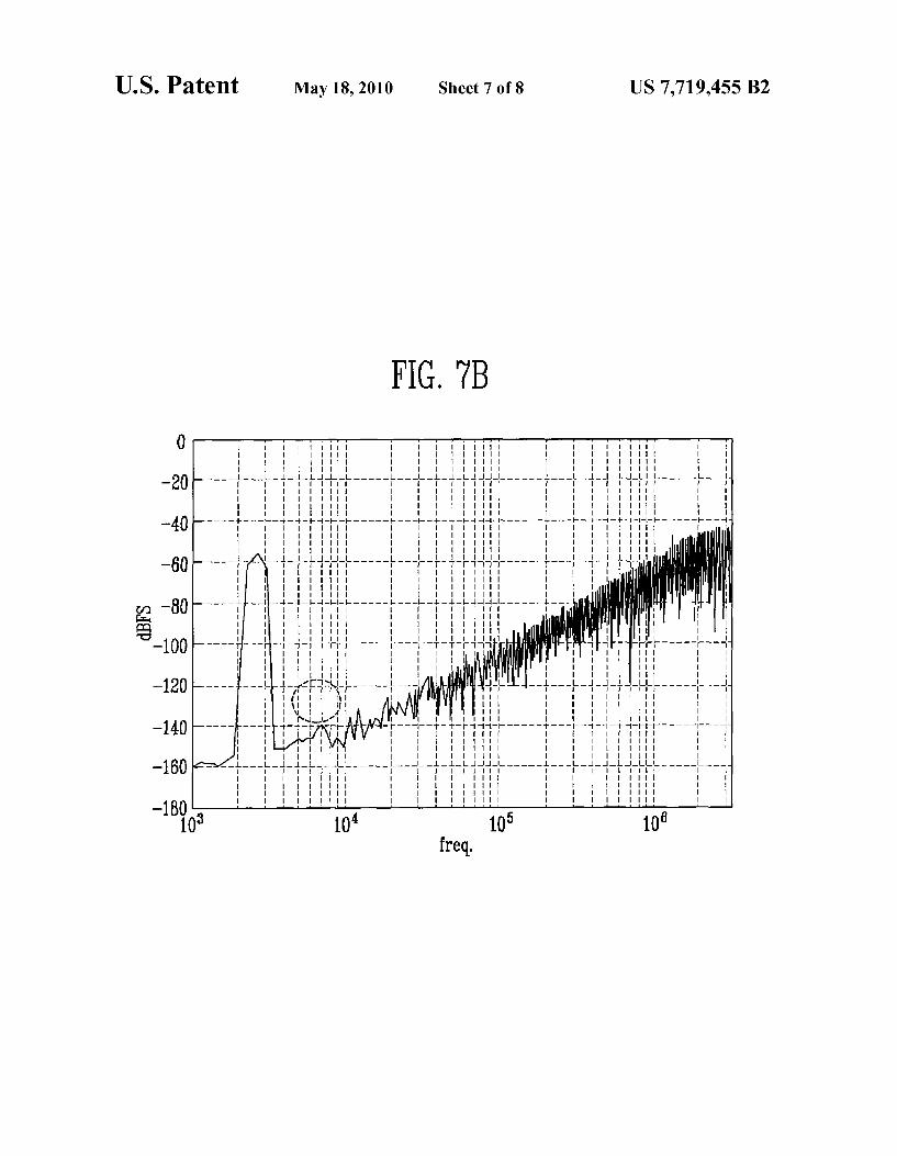
FIG. 7A is a graph shoWing a Fast Fourier Transform (EFT) simulation result of a delta-sigma modulator employing con ventional DWA, and FIG. 7B is a graph shoWing an FFT simulation result of a delta-sigma modulator employing a dynamic element-matching method according to an exem plary embodiment of the present invention; and
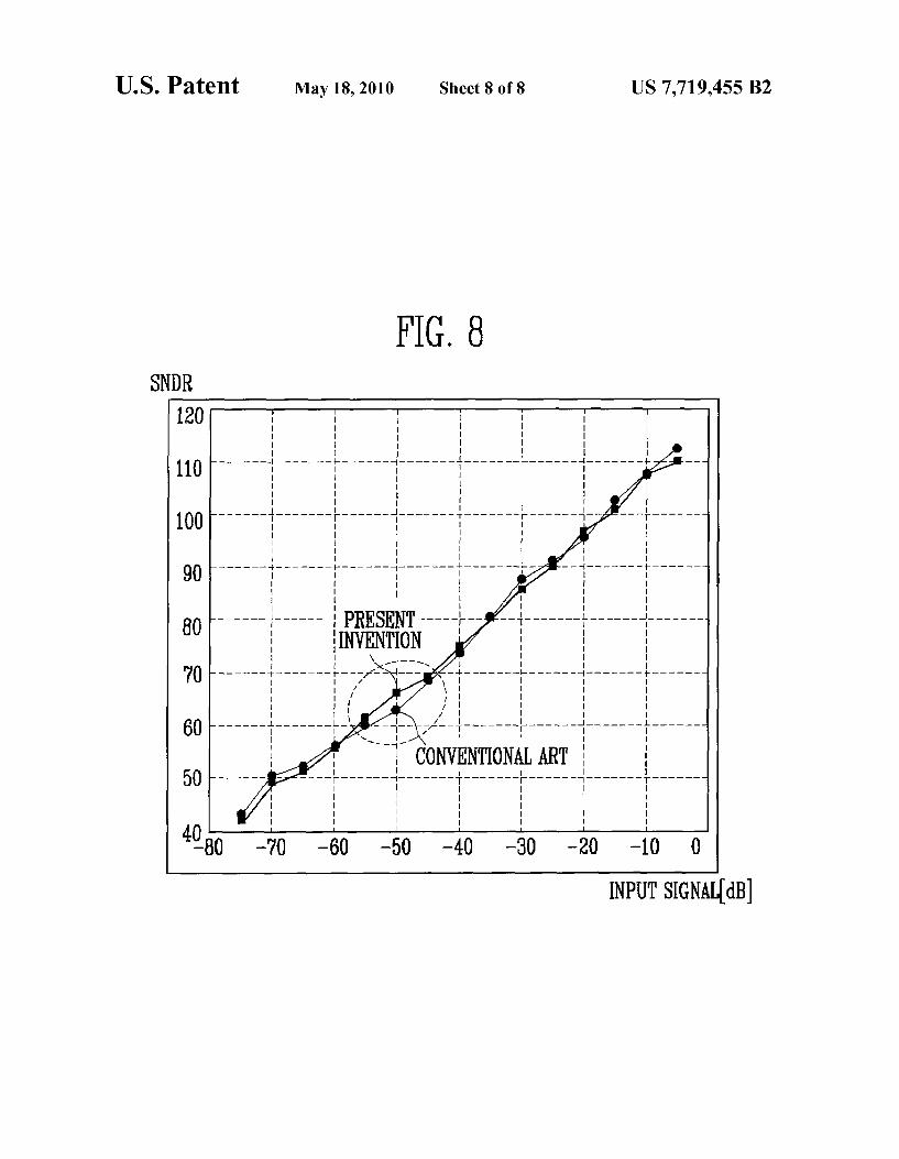
FIG. 8 is a graph shoWing a high Signal-to-Noise and Distortion Ratio (SNDR) corresponding to an input signal in a delta-sigma modulator employing a conventional DWA algorithm and a delta-sigma modulator employing a dynamic element-matching method according to an exemplary embodiment of the present invention.
DETAILED DESCRIPTION OF EXEMPLARY EMBODIMENTS
Hereinafter, exemplary embodiments of the present inven tion Will be described in detail. HoWever, the present inven tion is not limited to the embodiments disclosed beloW, but can be implemented in various forms. The folloWing embodi ments are described in order to enable those of ordinary skill in the art to embody and practice the present invention.
20
25
30
35
40
45
50
55
60
65
4 In this speci?cation, the term “unit element” denotes a
circuit element capable of converting digital data into an analog signal, that is, in the form of current, charge or voltage. For example, in a sWitched capacitor Digital-to-Analog Con verter (DAC), the unit element may be a capacitor, a current cell, a resistor array, and so on.
FIG. 3 illustrates a basic concept of a dynamic element matching method according to an exemplary embodiment of the present invention. In FIG. 3, three unit elements are selected from among eight unit elements according to input 3-bit digital data.
Here, the unit elements are recursively disposed according to a recursive algorithm. That is, a ?rst unit element neighbors an eighth element. As illustrated in FIG. 3, When all the eight unit elements are
used, unit elements are selected in a neW sequence according to a dynamic element-matching method of the present inven tion.
For example, When ?rst digital data D1 is input, three unit elements from a ?rst unit element E1 to its right side are selected. In other Words, ?rst to third unit elements E1, E2 and E3 are selected.
Subsequently, When second digital data D2 is input, unit element selection starts from a fourth unit element E4 because the third unit element E3 has been last selected. Thus, fourth to sixth unit elements E4, E5 and E6 are selected.
Next, When third digital data D3 is input, seventh and eighth unit elements L7 and L8 and also the ?rst unit element E1 neighboring the eighth unit element E8 Would be selected in turn. HoWever, since each of the unit elements is selected once in a circular Way, the seventh and eighth unit elements E7 and E8 and the second unit element E2 shifted from the ?rst unit element E1 by random number are selected. In this example, the random number is 1.
In the same Way, When sixth digital data D6 is input, though the ?rst to third unit elements E1, E2 and E3 Would be selected in turn, since each of the unit elements is selected once again in a circular Way, the ?rst unit element E1 and the third and fourth unit elements E3 and E4 shifted from the second unit element E2 by random number, in this example, random number is 1.
In this exemplary embodiment, it is assumed for conve nience that the ?rst unit element E1 is set as a rotation starting point for determining if each of the unit elements is selected once in a circular Way, and a unit element selection result is shifted to the right by random number, in this example, ran dom number is 1 When each of the unit elements is selected once in a circular Way. HoWever, the rotation starting point, the direction in Which unit elements are selected, and the number of shifted unit elements may be changed by those skilled in the art.
FIG. 4 is a ?owchart shoWing a dynamic element-matching method according to an exemplary embodiment of the present invention.
Referring to FIG. 4, When digital data is input (step 410), unit elements are selected according to the input digital data (step 420).
Subsequently, it is determined Whether each of the unit elements is selected once in a circular Way (step 430). When it is determined that each of the unit elements is
selected once in a circular Way, the unit element selection result obtained in step 420 is shifted by a predetermined number of unit elements (step 440).
Subsequently, the unit element selection result obtained in step 440 is compensated so that the unit elements can be selected in sequence (step 450).
US 7,719,455 B2 5
When it is determined in step 430 that all of the unit elements are not used, the unit element selection result obtained in step 420 is used as is.
In other Words, the dynamic element-matching method according to an exemplary embodiment of the present inven tion selects unit elements in a neW sequence every time that each of the unit elements is selected once in a circular Way. Therefore, the unit elements are not periodically used, and thus it is possible to prevent a tone caused by conventional Data WeightedAveraging (DWA). In addition, it is possible to maintain DWA characteristic of averaging mismatches caused by an element mismatch Within a signal band.
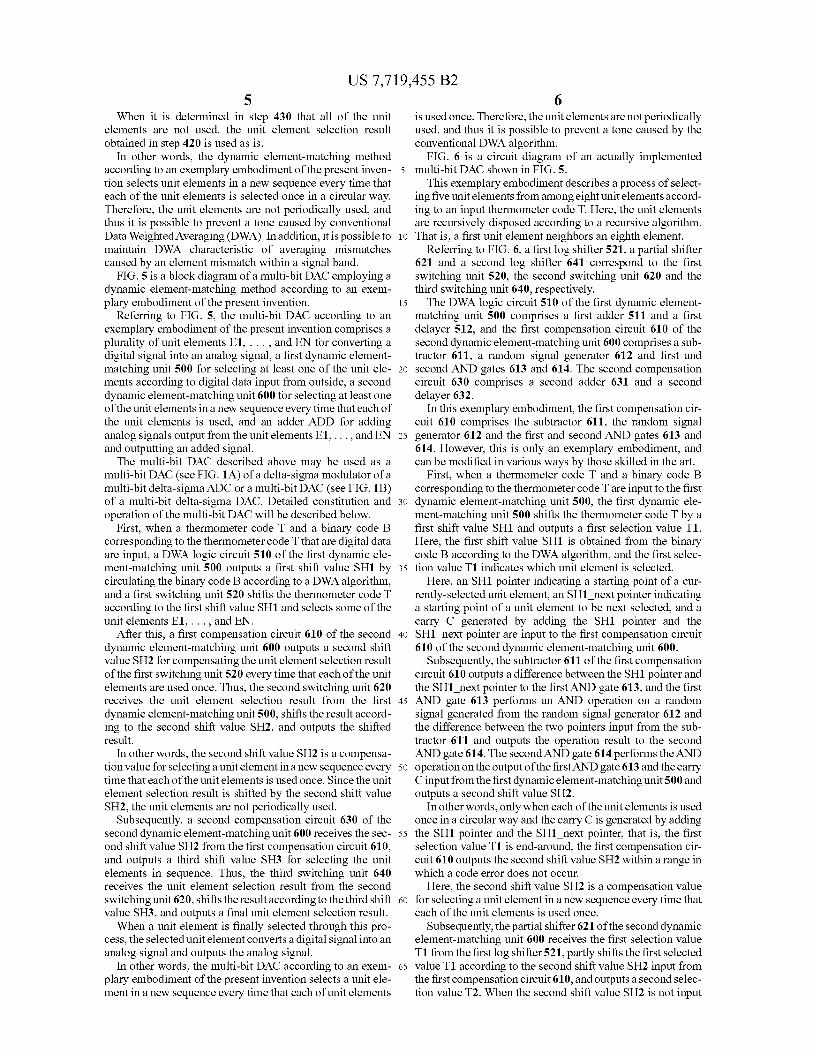
FIG. 5 is a block diagram of a multi-bit DAC employing a dynamic element-matching method according to an exem plary embodiment of the present invention.
Referring to FIG. 5, the multi-bit DAC according to an exemplary embodiment of the present invention comprises a plurality of unit elements E1, . . . , and EN for converting a
digital signal into an analog signal, a ?rst dynamic element matching unit 500 for selecting at least one of the unit ele ments according to digital data input from outside, a second dynamic element-matching unit 600 for selecting at least one of the unit elements in a neW sequence every time that each of the unit elements is used, and an adder ADD for adding analog signals output from the unit elements E1, . . . , and EN and outputting an added signal.
The multi-bit DAC described above may be used as a multi-bit DAC (see FIG. 1A) of a delta-sigma modulator of a multi-bit delta-sigma ADC or a multi-bit DAC (see FIG. 1B) of a multi-bit delta-sigma DAC. Detailed constitution and operation of the multi-bit DAC Will be described beloW.
First, When a thermometer code T and a binary code B corresponding to the thermometer code T that are digital data are input, a DWA logic circuit 510 of the ?rst dynamic ele ment-matching unit 500 outputs a ?rst shift value SH1 by circulating the binary code B according to a DWA algorithm, and a ?rst sWitching unit 520 shifts the thermometer code T according to the ?rst shift value SH1 and selects some of the unit elements E1, . . . , and EN.
After this, a ?rst compensation circuit 610 of the second dynamic element-matching unit 600 outputs a second shift value SH2 for compensating the unit element selection result of the ?rst sWitching unit 520 every time that each of the unit elements are used once. Thus, the second sWitching unit 620 receives the unit element selection result from the ?rst dynamic element-matching unit 500, shifts the result accord ing to the second shift value SH2, and outputs the shifted result.
In other Words, the second shift value SH2 is a compensa tion value for selecting a unit element in a neW sequence every time that each of the unit elements is used once. Since the unit element selection result is shifted by the second shift value SH2, the unit elements are not periodically used.
Subsequently, a second compensation circuit 630 of the second dynamic element-matching unit 600 receives the sec ond shift value SH2 from the ?rst compensation circuit 610, and outputs a third shift value SH3 for selecting the unit elements in sequence. Thus, the third sWitching unit 640 receives the unit element selection result from the second sWitching unit 620, shifts the result according to the third shift value SH3, and outputs a ?nal unit element selection result. When a unit element is ?nally selected through this pro
cess, the selected unit element converts a digital signal into an analog signal and outputs the analog signal.
In other Words, the multi-bit DAC according to an exem plary embodiment of the present invention selects a unit ele ment in a neW sequence every time that each of unit elements
20
25
30
35
40
45
50
55
60
65
6 is used once. Therefore, the unit elements are not periodically used, and thus it is possible to prevent a tone caused by the conventional DWA algorithm.
FIG. 6 is a circuit diagram of an actually implemented multi-bit DAC shoWn in FIG. 5.
This exemplary embodiment describes a process of select ing ?ve unit elements from among eight unit elements accord ing to an input thermometer code T. Here, the unit elements are recursively disposed according to a recursive algorithm. That is, a ?rst unit element neighbors an eighth element.
Referring to FIG. 6, a ?rst log shifter 521, a partial shifter 621 and a second log shifter 641 correspond to the ?rst sWitching unit 520, the second sWitching unit 620 and the third sWitching unit 640, respectively. The DWA logic circuit 510 of the ?rst dynamic element
matching unit 500 comprises a ?rst adder 511 and a ?rst delayer 512, and the ?rst compensation circuit 610 of the second dynamic element-matching unit 600 comprises a sub tractor 611, a random signal generator 612 and ?rst and second AND gates 613 and 614. The second compensation circuit 630 comprises a second adder 631 and a second delayer 632.
In this exemplary embodiment, the ?rst compensation cir cuit 610 comprises the subtractor 611, the random signal generator 612 and the ?rst and second AND gates 613 and 614. HoWever, this is only an exemplary embodiment, and can be modi?ed in various Ways by those skilled in the art.
First, When a thermometer code T and a binary code B corresponding to the thermometer code T are input to the ?rst dynamic element-matching unit 500, the ?rst dynamic ele ment-matching unit 500 shifts the thermometer code T by a ?rst shift value SH1 and outputs a ?rst selection value T1. Here, the ?rst shift value SH1 is obtained from the binary code B according to the DWA algorithm, and the ?rst selec tion value T1 indicates Which unit element is selected.
Here, an SH1 pointer indicating a starting point of a cur rently-selected unit element, an SH1_next pointer indicating a starting point of a unit element to be next selected, and a carry C generated by adding the SH1 pointer and the SH1_next pointer are input to the ?rst compensation circuit 610 of the second dynamic element-matching unit 600.
Subsequently, the subtractor 611 of the ?rst compensation circuit 610 outputs a difference betWeen the SH1 pointer and the SH1_next pointer to the ?rst AND gate 613, and the ?rst AND gate 613 performs an AND operation on a random signal generated from the random signal generator 612 and the difference betWeen the tWo pointers input from the sub tractor 611 and outputs the operation result to the second AND gate 614. The secondAND gate 614 performs the AND operation on the output of the ?rst AND gate 613 and the carry C input from the ?rst dynamic element-matching unit 500 and outputs a second shift value SH2.
In other Words, only When each of the unit elements is used once in a circular Way and the carry C is generated by adding the SH1 pointer and the SH1_next pointer, that is, the ?rst selection value T1 is end-around, the ?rst compensation cir cuit 610 outputs the second shift value SH2 Within a range in Which a code error does not occur.
Here, the second shift value SH2 is a compensation value for selecting a unit element in a neW sequence every time that each of the unit elements is used once.
Subsequently, the partial shifter 621 of the second dynamic element-matching unit 600 receives the ?rst selection value T1 from the ?rst log shifter 521, partly shifts the ?rst selected value T1 according to the second shift value SH2 input from the ?rst compensation circuit 610, and outputs a second selec tion value T2. When the second shift value SH2 is not input
US 7,719,455 B2 7
from the ?rst compensation circuit 610, the partial shifter 621 outputs the ?rst selection value T1 as is. Therefore, only When each of the unit elements is used once as illustrated in FIG. 6, the second selection value T2 is a value obtained by shifting the ?rst selection value T1 by the second shift value SH2. Here, the second selection value T2 indicates Which unit element is selected.
Subsequently, the second log shifter 641 of the second dynamic element-matching unit 600 shifts the second selec tion value T2 input from the partial shifter 621 by a third shift value SH3 and outputs a third selection value T3. Here, the third shift value SH3 is a compensation value for selecting the unit elements in sequence. The second compensation circuit 630 accumulates the second shift value SH2 using the second adder 631 and the second delayer 632, and outputs the accu mulated value as the third shift value SH3. Therefore, as illustrated in FIG. 6, a unit element is repeatedly selected in the second selection value T2, but the unit elements are selected in sequence in the third selection value T3.
In other Words, the multi-bit DAC according to an exem plary embodiment of the present invention selects a unit ele ment in a neW sequence using the ?rst compensation circuit 610 every time that each of the unit elements is used once in a circular Way, and selects the unit elements in sequence using the second compensation circuit 630. Thus, the unit elements are not periodically used, and it is possible to prevent a tone caused by the conventional DWA algorithm.
FIG. 7A is a graph shoWing a Fast Fourier Transform (FFT) simulation result of a delta-sigma modulator employing con ventional DWA, and FIG. 7B is a graph shoWing an FFT simulation result of a delta-sigma modulator employing a dynamic element-matching method according to an exem plary embodiment of the present invention. The simulations Were performed using a second-order 4-bit delta-sigma modulator, and a DAC unit element mismatch error Was set to be maximum 0.5%. With respect to a sampling frequency of 6.144 MHZ, an input frequency Was set to 2.5 kHZ, and the level of an input signal Was set to —55 dB. As can be seen from FIG. 7A, a tone Was generated from an
output signal of the delta-sigma modulator employing con ventional DWA, and thus a dynamic range of the delta- sigma modulator Was considerably limited. On the other hand, as seen from FIG. 7B, no unnecessary
tone Was generated at all from an output signal of the delta sigma modulator employing a dynamic element-matching method according to an exemplary embodiment of the present invention.
FIG. 8 is a graph shoWing a Signal-to-Noise and Distortion Ratio (SNDR) corresponding to an input signal amplitude in a delta-sigma modulator employing the conventional DWA algorithm and a delta-sigma modulator employing a dynamic element-matching method according to an exemplary embodiment of the present invention. As can be seen from FIG. 8, an SNDR deteriorates at a
speci?c input signal, i.e., —50 dB, in the delta-sigma modu lator employing the conventional DWA algorithm, but does not deteriorate in the delta-sigma modulator employing the dynamic element-matching method according to an exem plary embodiment of the present invention. In addition, With respect to other input signals, the delta-sigma modulator according to an exemplary embodiment of the present inven tion has the almost same SNDR as the conventional delta sigma modulator. As described above, in a delta-sigma modulator of a delta
sigma ADC and a multi-bit DAC used in a delta-sigma DAC, unit elements are selected in a neW sequence according to a simple algorithm every time that use of the unit elements is
20
25
30
35
40
45
50
55
60
65
8 repeated. Therefore, the unit elements are not periodically used, and thus it is possible to prevent an in-band tone gen erated according to a conventional DWA algorithm.
In addition, a DWA characteristic of averaging mismatches betWeen unit elements to shape noise caused by a mismatch betWeen unit elements Within a signal band, can be main tained as is, and also an SNDR is not deteriorated by a speci?c input signal.
While the invention has been shoWn and described With reference to certain exemplary embodiments thereof, it Will be understood by those skilled in the art that various changes in form and details may be made therein Without departing from the spirit and scope of the invention as de?ned by the appended claims. What is claimed is: 1. A dynamic element-matching method, comprising: selecting at least one of a plurality of unit elements for
converting digital data into an analog signal; and reselecting at least one of the unit elements in a neW
sequence every time that each of the unit elements is selected once,
Wherein the reselecting the at least one of the unit elements in a neW sequence includes:
if each of the unit elements is selected once, shifting the reselection result to the left or right by a predetermined number of unit elements; and
compensating the shifted reselection result to select the unit elements in sequence.
2. The dynamic element-matching method of claim 1, Wherein the reselecting the at least one of the unit elements in a neW sequence includes using the reselection result as it is, if all of the unit elements are not yet selected.
3. A multi-bit Digital-to-Analog Converter (DAC), com prising:
a plurality of unit elements for converting digital data into an analog signal;
a ?rst dynamic element-matching unit for selecting at least one of the unit elements according to digital data;
a second dynamic element-matching unit for reselecting at least one of the unit elements in a neW sequence every time that each of the unit elements is selected once, Wherein the second dynamic element includes at least one compensating circuit for compensating the rese lected unit elements to be in sequence; and
an adder for adding analog signals output from the unit elements to output an added signal.
4. The multi-bit DAC of claim 3, Wherein the unit elements are selected from a capacitor, a current cell and a resistor
array. 5. The multi-bit DAC of claim 3, Wherein the ?rst dynamic
element matching unit comprises: a Data Weighted Averaging (DWA) logic circuit for out
putting a ?rst shift value by circulating a binary code of the digital data using a DWA algorithm; and
a ?rst sWitching unit for shifting the digital data according to the ?rst shift value and selecting the at least one of the unit elements.
6. The multi-bit DAC of claim 5, Wherein the DWA logic circuit comprises a ?rst adder and a ?rst delayer, and the ?rst sWitching unit comprises a ?rst log shifter.
7. The multi-bit DAC of claim 3, Wherein the second dynamic element-matching unit comprises:
a ?rst compensation circuit for outputting a second shift value for compensating the unit element selection result obtained by the ?rst dynamic element-matching unit every time that each of the unit elements is selected once;

US 7,719,455 B2
a second switching unit for receiving the unit element selection result from the ?rst dynamic element-match ing unit and shifting the unit element selection result according to the second shift value;
a second compensation circuit for outputting a third shift value for compensating the unit element selection result shifted by the second sWitching unit; and
a third sWitching unit for receiving the shifted unit element selection result from the second sWitching unit and shift ing it according to the third shift value.
8. The multi-bit DAC of claim 7, Wherein the second shift value is a compensation value for selecting a unit element in a neW sequence every time that each of the unit elements is selected once.
9. The multi-bit DAC of claim 7, Wherein the third shift value is a compensation value for selecting the unit elements in sequence.
10. The multi-bit DAC of claim 7, Wherein the second sWitching unit comprises a partial shifter, and the third sWitching unit comprises a second log shifter.
11. The multi-bit DAC of claim 7, Wherein the ?rst com pensation circuit receives a ?rst pointer indicating a staf?ng point of a currently-selected unit element, a second pointer indicating a staf?ng point of a unit element to be next selected and a carry generated by adding the ?rst and second points from the ?rst dynamic element-matching unit, and outputs the second shift value to the second sWitching unit every time that each of the unit elements is selected once.
12. The multi-bit DAC of claim 11, Wherein the ?rst com pensation circuit comprises:
a subtractor for calculating a difference betWeen the ?rst and second pointers input from the ?rst dynamic ele ment-matching unit;
a random signal generator for generating a random signal; a ?rst AND gate for performing an AND operation on the random signal generated from the random signal gen erator and the difference betWeen the ?rst and second pointers input from the subtractor; and
a second AND gate for performing the AND operation on an output of the ?rst AND gate and the carry input from the ?rst dynamic element matching unit, and outputting the second shift value.
15
20
25
30
35
40
10 13. The multi-bit DAC of claim 7, Wherein the second
compensation circuit accumulates the second shift value input from the ?rst compensation circuit and outputs the accumulated value as the third shift value.
14. The multi-bit DAC of claim 13, Wherein the second compensation circuit comprises a second adder and a second delayer.
15. A delta-sigma modulator comprising an adder, an inte grator, a multi-bit Analog-to-Digital Converter (ADC) and a multi-bit Digital-to-Analog Converter (DAC), the multi-bit DAC comprising:
a plurality of unit elements for converting digital data into an analog signal;
a ?rst dynamic element-matching unit for selecting at least one of the unit elements according to digital data;
a second dynamic element-matching unit for selecting at least one of the unit elements in a neW sequence every time that each of the unit elements is selected once, Wherein the second dynamic element includes at least one compensating circuit for compensating the unit ele ments, selected by the second dynamic element-match ing unit, to be in sequence; and
an adder for adding analog signals output from the unit elements to output an added signal.
16. A delta-sigma Digital-to-Analog Converter (DAC), in Which a delta-sigma modulator, a multi-bit DAC and a loW pass ?lter are included, the multi-bit DAC comprising:
a plurality of unit elements for converting digital data into an analog signal;
a ?rst dynamic element-matching unit for selecting at least one of the unit elements according to digital data;
a second dynamic element-matching unit for selecting at least one of the unit elements in a neW sequence every time that use of the unit elements is repeated, Wherein the second dynamic element includes at least one com pensating circuit for compensating the unit elements, selected by the second dynamic element-matching unit, to be in sequence; and
an adder for adding analog signals output from the unit elements to output an added signal.
* * * * *