Embed Size (px)
Citation preview

University of Twente
Faculty of Electrical Engineering,Mathematics & Computer Science
Design of an Oscillator for
Satellite Reception
Frank Leong
M.Sc. ThesisOctober 2007
Supervisors:dr. ir. D.M.W. Leenaerts
ir. P.F.J. Geraedtsprof. dr. ir. B. Nauta
dr. ing. E.A.M. Klumperink
Report number: 067.3229 Chair of Integrated Circuit DesignFaculty of Electrical Engineering,Mathematics & Computer Science
University of TwenteP. O. Box 217
7500 AE EnschedeThe Netherlands

Abstract
This thesis presents research on an LC-oscillator for Ku-band (10.7-12.7GHz) satellitereception. The zero-IF receiver architecture, proposed in the joint project involving theUniversity of Twente and NXP Research, requires a 11.7GHz quadrature oscillator thatachieves a phase noise of -85dBc/Hz@100kHz and an IRR of 30dB. Such an oscillator wasdesigned in an NXP 65nm CMOS process.
The performance of three types of LC-oscillators was compared: the Colpitts topology,the cross-coupled pair topology and a new topology, the crossed-capacitor oscillator. Bothsingle and quadrature oscillator simulations were compared. Although the cross-coupledpair topology can achieve the highest FoM and the quadrature crossed-capacitor oscillatorcan achieve the highest IRR, the Colpitts oscillator was selected and developed, due toits reasonable IRR performance and its ability to run at a higher supply voltage than thecross-coupled pair oscillator, allowing sufficient phase noise performance.
Development includes the design of a suitable buffer, a frequency tuning mechanism,and circuitry allowing the measurement of oscillation frequency and quadrature accuracy.Simulated performance and schematics are presented.


Contents
Preface . . . . . . . . . . . . . . . . . . . . . . . . . . . . . . vii
1 Introduction . . . . . . . . . . . . . . . . . . . . . . . . . . . . 1
2 Assignment Overview . . . . . . . . . . . . . . . . . . . . . . . . 3
3 Oscillator Models . . . . . . . . . . . . . . . . . . . . . . . . . . 9
3.1 General Aspects of Oscillators . . . . . . . . . . . . . . . . . . . . 93.1.1 Tank Losses and Impedance Transformations . . . . . . . . . . . 103.1.2 Startup . . . . . . . . . . . . . . . . . . . . . . . . . . 113.1.3 Phase Noise . . . . . . . . . . . . . . . . . . . . . . . . 12
3.2 Specific Oscillator Types . . . . . . . . . . . . . . . . . . . . . . 143.2.1 Cross-Coupled Pair and Colpitts Oscillators . . . . . . . . . . . 143.2.2 Crossed-Capacitor Oscillator. . . . . . . . . . . . . . . . . . 15
3.3 Quadrature Oscillators . . . . . . . . . . . . . . . . . . . . . . . 173.3.1 General Considerations Concerning Quadrature Coupling . . . . . . 173.3.2 Practical Implementations of Quadrature Coupling . . . . . . . . . 23
4 Buffer Design. . . . . . . . . . . . . . . . . . . . . . . . . . . . 27
4.1 Small-Signal Buffer Models . . . . . . . . . . . . . . . . . . . . . 274.1.1 Common-Source Amplifier . . . . . . . . . . . . . . . . . . 274.1.2 Source Follower . . . . . . . . . . . . . . . . . . . . . . . 30
4.2 Practical Buffers . . . . . . . . . . . . . . . . . . . . . . . . . 31
5 Inductor Design . . . . . . . . . . . . . . . . . . . . . . . . . . 33
6 Frequency Tuning . . . . . . . . . . . . . . . . . . . . . . . . . . 35
6.1 Tuning Linearity . . . . . . . . . . . . . . . . . . . . . . . . . 38
7 Results. . . . . . . . . . . . . . . . . . . . . . . . . . . . . . . 39
8 Benchmarking . . . . . . . . . . . . . . . . . . . . . . . . . . . 49
9 Conclusion . . . . . . . . . . . . . . . . . . . . . . . . . . . . . 51
References . . . . . . . . . . . . . . . . . . . . . . . . . . . . . 53
v

vi CONTENTS
Appendices
A Derivation ISF of LC-Oscillator . . . . . . . . . . . . . . . . . . . 57
A.1 Definitions . . . . . . . . . . . . . . . . . . . . . . . . . . . 57A.2 Derivation. . . . . . . . . . . . . . . . . . . . . . . . . . . . 58A.3 Correction for Large Impulses . . . . . . . . . . . . . . . . . . . . 59
B On Constant Quadrature Currents . . . . . . . . . . . . . . . . . . 61
C CCO and Process Scaling . . . . . . . . . . . . . . . . . . . . . . 63
D Estimation of Parasitic Inductance . . . . . . . . . . . . . . . . . . 65
E Fine Tuning Script Colpitts QDCO . . . . . . . . . . . . . . . . . . 67
F Coarse Tuning Script Colpitts QDCO. . . . . . . . . . . . . . . . . 73

Preface
At the beginning of 2007, I knew almost nothing about satellite receivers, so when BramNauta suggested, for the Master’s thesis, work on a CMOS satellite receiver at NXPResearch in Eindhoven, I thought it would be an interesting challenge. And it was, fromthe start of the project on March 15 until the end. It was a privilege to have as a dailysupervisor as competent a man as Domine Leenaerts; Domine, thank you for teaching meso many things that are found in no textbook.
The final chip makes use of work from various other people. I would like to thank thepeople at the IRFS group of NXP Research for supplying the project with designs,discussions, and suggestions.
Finally, I must apologize to any potential reader that this report is so limited in bothscope and content. There is much more to be said about integrated oscillators in generaland the project in particular.
Frank LeongEnschede, September 22nd, 2007
Das rein intellektuelle Leben der Menschheit besteht in ihrer fortschreitenden Erkenntnismittelst der Wissenschaften und in der Vervollkommnung der Kunste, welche Beide, Men-schenalter und Jahrhunderte hindurch, sich langsam fortsetzen, und zu denen ihren Beitragliefernd, die einzelnen Geschlechter vorubereilen. Dieses intellektuelle Leben schwebt, wieeine atherische Zugabe, [...] uber dem weltlichen Treiben, dem eigentlich realen, vomWillen gefuhrten Leben der Volker, und neben der Weltgeschichte geht schuldlos undnicht blutbefleckt die Geschichte der Philosophie, der Wissenschaft und der Kunste.
– Arthur Schopenhauer
A science is said to be useful if its development tends to accentuate the existing inequalitiesin the distribution of wealth, or more directly promotes the destruction of human life.
– Godfrey Harold Hardy
vii


Chapter 1
Introduction
Nowadays, many homes have access to television broadcasts, which are usually receivedusing a fixed terrestrial coaxial cable. Terrestrial antenna solutions have generally beenavoided, as they suffer from interference; digital standards are changing this. Anotheroption is receiving broadcasts using a satellite dish, pointed at a satellite in space on ageosynchronous orbit in the Clarke Belt, which does not require a dedicated cable froma broadcasting node to the home and therefore gives the television viewer an additionaldegree of flexibility.
Although picture quality from satellite receivers is generally considered very good, theequipment is relatively expensive, as many required analog components are quite exotic.High electron-mobility transistor (HEMT) amplifier modules are required to achieve thedesired noise level and dielectric resonator oscillators (DRO) are required to achieve thedesired spectral purity in the downconversion stage. In addition, these components areonly available as discrete building blocks, so some microwave engineering is required tominimize losses and interference in the layout of the high-frequency part. Furthermore,the Low-Noise-Block (LNB) and the decoder are generally seperated into what are knownas Out-Door-Unit (ODU) and In-Door-Unit (IDU). These two parts are connected by a(lossy) cable, commonly a popular type such as RG-59/U (loss: 8.2dB/30m@1GHz) orRG-11/U (loss: 4.3dB/30m@1GHz), with (lossy) F-connectors mounted at the ends. Thecable usually feeds a DC voltage of 14V or 18V to the LNB, necessitating an additionalsupply line in the decoder. For these reasons, a satellite receiver is far more costly toproduce and install than an ordinary television tuner.
For a long time now, CMOS processes have been continuously downscaling to ever smaller(minimum) transistor lengths and thinner gate oxides, resulting in faster and more accu-rate ADCs. We are at a point where direct conversion of the entire Ku-band has becomean option. Without intermediate IF-stages, slightly weaker oscillator performance figurescan be tolerated and making the entire RF-to-baseband conversion in one reasonably-sizedCMOS chip is therefore an option. With a one-chip CMOS satellite solution, productionand installation costs of satellite receivers would drop significantly, flexibility due to inte-gration potential would increase (a Wi-Fi signal could come straight from the dish) andconsequently satellite receivers could become even more popular than they are today, fit-ting into the general trend of the wired-to-wireless shift (e.g. USB to UWB and LAN toWLAN). Imagine watching satellite TV on your PDA (see Figure 1.1) or an entire hotelwith thousands of guests requiring only one satellite dish!
The focus of this report is the development of a suitable, digitally controllable, oscillator.
1

2 CHAPTER 1. INTRODUCTION
Figure 1.1: Satellite receiver as part of the wireless home network.
For direct conversion, a quadrature oscillator is required, which locks onto an externalquartz crystal by means of a Phase-Locked Loop (PLL).
The oscillator is designed in a 65nm CMOS process. While this process provides largeamounts of transconductance gain due to high gate oxide capacitance and the high W/Lratios that are possible with the nominal channel length of 60nm, reliability issues form abottleneck; DC voltages over the gate oxide of only 1.2V are allowed. In addition, short-channel effects give the minimum-length transistors highly nonlinear output impedancesand the interconnect can introduce very substantial parasitics. All these factors make itchallenging to design a robust oscillator. Where normally the focus of an oscillator designis on power consumption, the main concern in this project is simply to be able to meetthe performance requirements.
The report is built up as follows. First, an overview of the assignment and the satellitesystem is given in Chapter 2. Chapter 3 reviews basic oscillator theory and some relevantadditions that have emerged in both the literature and the current work. The buffer isdescribed in Chapter 4. Next, Chapter 5 presents the inductor model and design, followedby a description of the frequency tuning in Chapter 6. In Chapter 7 the final design, layoutand simulation results are presented, which are compared with literature in Chapter 8.Chapter 9 summarizes the findings and gives some recommendations for improvements.

Chapter 2
Assignment Overview
The focus of this report is on an oscillator, which is intended to be part of a larger zero-IFreceiver system. Schematically, this is shown in Figure 2.1. The LO block, including the90 degree phase shift, is the subject of this work.
pHEMT
A
D
LO
11.7GHz
A
D
pHEMT
A
D
A
D
H
V
QH
IV
1.05 GHz
1.05 GHz
1.05 GHz
1.05 GHz
2.1 Gs/s 8 bit
2.1 Gs/s 8 bit
2.1 Gs/s 8 bit
50 MHz
Zero-IFTopology
2.1 Gs/s 8 bit
CMOS
+900
IH
QV
Figure 2.1: Zero-IF satellite receiver block model.
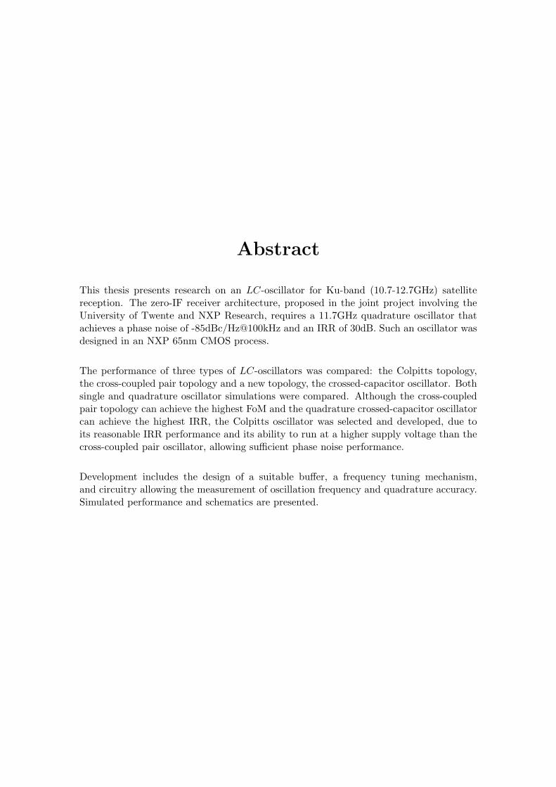
The zero-IF structure requires two ADCs per signal chain instead of one, but the requiredbandwidths of the ADCs are only approximately half as large as the required bandwidthof an ADC in a low-IF solution. This is depicted in Figure 2.2.
Oscillators have been part of RF receivers since Armstrong patented the superheterodynereceiver in the year 1919. Since then, the qualities of quartz-based oscillators have beenappreciated and many current oscillators depend on such crystals for frequency consistency.As quartz crystals resonate only at a very limited set of frequencies, receivers are generally
3
4 CHAPTER 2. ASSIGNMENT OVERVIEW
0 ω →
↑ P (ω)
0 ω →
↑ Pdownconverted(ω)
ωs,l/2
(a) Low-IF Topology.
0 ω →
↑ P (ω)
0 ω →
↑ Pdownconverted(ω)
ωs,z/2
(b) Zero-IF Topology.
Figure 2.2: Spectra due to downconversion in two different schemes. The rectangular blocksrepresent the signal spectrum of the Ku-band, the arrows the LO frequencies, and the dottedlines the anti-aliasing filters preceding the ADCs. Clearly visible is the difference in minimumsampling rate; a lower rate also simplifies filter design.
built using a higher-frequency voltage-controlled LC- or ring-oscillator, connected througha frequency divider in a Phase-Locked Loop (PLL) with the crystal. This method combinesthe flexibility of LC-/ring-oscillators with the good temperature/drift properties of thequartz crystal.
For a satellite receiver, good spectral purity is required to meet specifications (from expe-rience, a phase noise of -85dBc/Hz@100kHz or better is considered necessary for a VCOin a PLL) and therefore a common LNB uses a DRO that performs very well, but is quitecostly to fabricate and calibrate in comparison with an integrated solution. The challengein this project is to create an on-chip oscillator that can replace this component and ismade in CMOS for large-scale integration.
The set of components that are available on-chip is rather limited. Fortunately, it ispossible to make high-quality inductors and accurate models exist to describe them [4].In addition, several varieties of transistors, capacitors and resistors exist. The inductorsconsume the most area and place the most constraints on the rest of the architecture.Therefore, the inductors are designed first, with the rest of the circuit matched to theinductor’s unavoidable parasitics. As the inductor design is rather involved by itself, thisstep is described separately in Chapter 5. The influence on the oscillator of potentialinductor parasitics is described first, in Chapter 3. That chapter is followed directly by adescription of one of the most power-hungry circuit blocks, the buffer, in Chapter 4. Thelast circuit block to be described is the frequency tuning mechanism in Chapter 6, as it isdesigned last.
As can be seen in Figure 2.1, the oscillator is not directly in the signal path of the satellitereceiver. Nonetheless, its properties have a huge influence on the quality of the signalthat is fed into the ADC, since any impurities in either frequency, phase or amplitude (of

5
course amplitude information is less relevant in case of a hard-switching mixer) will betransferred to the signal in the mixer stage. Especially since the system is of the zero-IFtype, the oscillator is important, as the quadrature angle might limit the performance ofthe receiver.
The analysis of the quadrature downmixed signal outputs, for both positive and negativeangular frequency offsets, makes use of the trigonometric identity
cos(u)·cos(v) =12
[cos(u− v) + cos(u + v)
](2.1)
and follows below. The approximations are valid if the output signal is lowpass filtered,i.e. components around twice the oscillator frequency are removed.
cos(ω0·t + ∆ω·t)·cos(ω0·t) =12
[cos(∆ω·t) + cos(2ω0·t + ∆ω·t)
]≈ 1
2cos(∆ω·t). (2.2)
cos(ω0·t + ∆ω·t)·cos(ω0·t +π
2) =
12
[cos(∆ω·t− π
2) + cos(2ω0·t + ∆ω·t +
π
2)]
≈ 12cos(∆ω·t− π
2). (2.3)
cos(ω0·t−∆ω·t)·cos(ω0·t) =12
[cos(∆ω·t) + cos(2ω0·t−∆ω·t)
]≈ 1
2cos(∆ω·t). (2.4)
cos(ω0·t−∆ω·t)·cos(ω0·t +π
2) =
12
[cos(∆ω·t +
π
2) + cos(2ω0·t−∆ω·t +
π
2)]
≈ 12cos(∆ω·t +
π
2). (2.5)
This results in the I and Q output signals, given in (2.6) and (2.7), for input signals withrespectively positive and negative angular frequency offsets from the LO frequency. Notethat, in principle, it makes no difference if the signal is in quadrature (difficult to achieveover a wide frequency band with the desired noise figure) or the oscillator is in quadrature.
+ ∆ω : I≈12cos(∆ω·t), Q≈1
2cos(∆ω·t− π
2). (2.6)
−∆ω : I≈12cos(∆ω·t), Q≈1
2cos(∆ω·t +
π
2). (2.7)
Therefore it simply remains to implement a 90 degrees phase shifter to distinguish betweenpositive and negative frequency offsets. If the Q signal is shifted by +π
2 and added to theI signal, the signal with positive frequency offset will be transferred and the signal with

6 CHAPTER 2. ASSIGNMENT OVERVIEW
negative frequency offset will be added to its 180 degrees shifted version, resulting in zerooutput. The opposite happens for a −π
2 phase shift in the Q path, or, perhaps moreconvenient, a +π
2 phase shift in the I path. The latter solution is easily implemented by aHilbert transformer that can be switched between the I and the Q paths. The principle isillustrated in Figure 2.3. The phase shifters are easily implemented digitally, where theycan be used in parallel, such that the whole band can be received all the time.
SignalI
+90°
SignalQ
+Signal+ f
SignalQ
+90°
SignalI
+Signal- f
Figure 2.3: Switching of the phase shifter to receive both upper and lower band.
Of course the angle of 90 degrees between the different oscillator outputs is in reality notperfect and there will also be a certain amplitude mismatch between the different oscillatoroutputs. This means that a certain amount of leakage can occur from negative to positivefrequency offsets and vice versa, causing distortion of the desired signal by an unwantedimage. The quality of the quadrature angle and the amplitude mismatch determine theso-called Image-Rejection Ratio (IRR). It is defined as follows (as in, for instance, [17]),where ε is the relative amplitude mismatch and φ is the phase deviation from perfectquadrature in radians.
IRR =Psig,out
Pim,out×
A2im,in
A2sig,in
≈ 4ε2 + φ2
. (2.8)
In practice, the mixers are clipping, making the outputs dependent only on the zero-crossings of the inputs, eliminating amplitude mismatches and therefore making the IRRdependent solely on φ. From previous experience, a goal of 30dB IRR (corresponding toa quadrature accuracy better than 3.62 degrees) is set.
Although RC polyphase filters may be used to derive 90 degrees phase shifted outputsfrom a single oscillator [25] [26], these filters generally require more power due to additionalbuffering and suffer from relatively poor IRR due to process spread, very unfavorable inbulk CMOS, and component mismatch, consequence of the small time constants necessaryin this project. Therefore this type of solution was not investigated further.

7
In principle, it is also possible to generate quadrature signals from a single oscillator run-ning at twice the required output frequency. Two dividers, one triggered by the positiveedges of the oscillator, and the other triggered by the negative edges of the oscillator,produce quadrature outputs. In practice, dividers with coils produce spurs on the oscilla-tor, and dividers without coils can be considered as injection-locked RC-oscillators, witha very large power consumption for the desired frequency and noise level. In addition,this solution is very sensitive to transistor mismatch and layout parasitics, making it verydifficult to achieve an accurate quadrature angle. For the above reasons, this option wasnot developed.
The quadrature accuracy cannot be measured properly off-chip. Because a cable lengthasymmetry of 1cm will already introduce approximately 50ps of propagation delay dif-ference [18, p. 18], and the oscillator period is approximately 85ps, the equipment willmeasure the setup, rather than the oscillator.
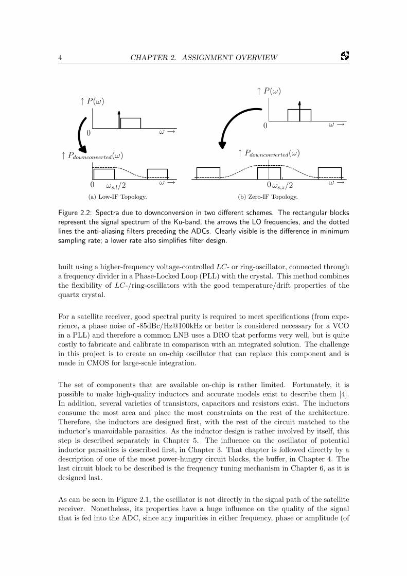
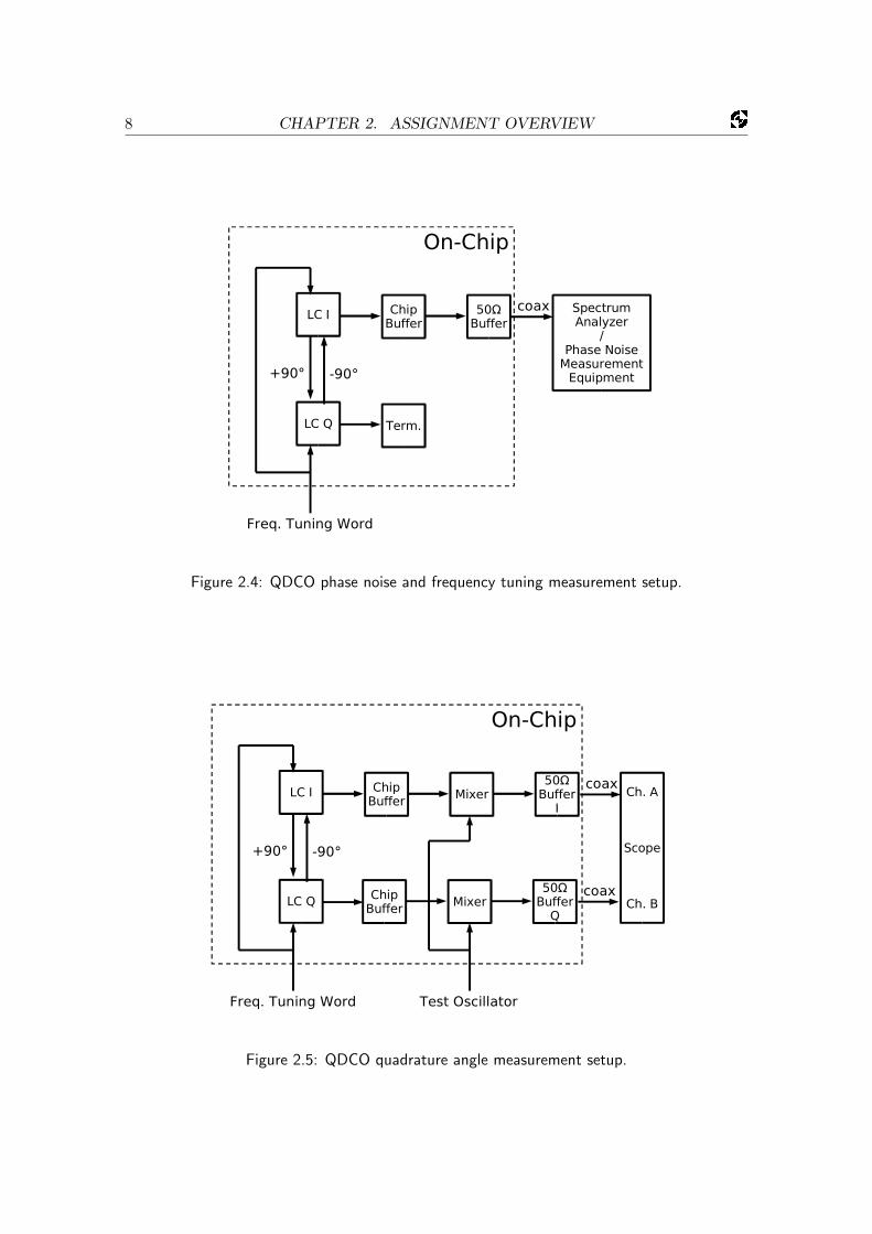
By adding a mixer on-chip to downmix the quadrature to a frequency near DC, thequadrature angle will still be contained in the output signals (inspecting (2.2) and (2.3)will yield this result) and can be measured without any relevant cable delays. For thisreason, two test circuits are designed in this assignment: one to measure the frequency,as shown in Figure 2.4, and one to measure quadrature accuracy, as shown in Figure 2.5.Note that the frequency of the oscillator is controlled digitally; the oscillator is thereforeclassified as a Quadrature Digitally Controlled Oscillator (QDCO).
To summarize, the goals of the work are as follows:
- Design a suitable (L(100kHz) = −85dBc/Hz, 30dB IRR) oscillator at 11.7GHz;
- Include a frequency tuning mechanism that can be interfaced to a PLL to make thefrequency accurate and stable;
- Design a suitable chip buffer to drive the PLL phase detector, mixers, and linedrivers;
- Make a top-level test layout that allows the concept to be measured properly.
The oscillator is to be fabricated in a baseline 65nm CMOS process (allowing a DC voltageof 1.2V across gate oxides and a maximum RF swing exceeding this voltage by approxi-mately 50%) with the option of a second gate-oxide process step (GO2), allowing the useof 2.5V MOST devices in the design.
8 CHAPTER 2. ASSIGNMENT OVERVIEW
LC I
LC Q
-90°+90°
Freq. Tuning Word
50Buffer
Term.
SpectrumAnalyzer
/Phase Noise
MeasurementEquipment
coaxChipBuffer
On-Chip
Figure 2.4: QDCO phase noise and frequency tuning measurement setup.
LC I
LC Q
Freq. Tuning Word
50Buffer
I
Ch. A
Scope
Ch. B
coaxChipBuffer
Mixer
ChipBuffer
Mixer
Test Oscillator
On-Chip
50Buffer
Q
coax
-90°+90°
Figure 2.5: QDCO quadrature angle measurement setup.

Chapter 3
Oscillator Models
In this chapter, first abstract circuit models relevant to oscillator design are presented inSection 3.1, followed by specific implementations of single and quadrature oscillators inSections 3.2 and 3.3, respectively.
3.1 General Aspects of Oscillators
There are basically two types of oscillator, RC-oscillators, such as ring-oscillators basedon inverters, and LC-oscillators (crystals are in fact modeled as LC-resonators). Both areapplied in ICs, but RC-oscillators have inferior phase-noise performance at a given powerbudget and are therefore not very good candidates for this project.
LC-oscillators work on a rather intriguing principle, illustrated in Figure 3.1.
C L
i
+
_
v
0t →
↑ v
0t →
↑ i
Figure 3.1: Basic LC oscillator tank with waveforms for a certain initial current.
For a certain resonance frequency, the impedance of the parallel LC-tank becomes infinite(equivalently, its series impedance becomes zero!) and when energy is stored in the tank, itcirculates from voltage energy in the capacitor (1
2Cv2) to current energy in the coil (12Li2)
9

10 CHAPTER 3. OSCILLATOR MODELS
and vice versa, at precisely the resonance frequency ω0 = 1/√
LC , with the voltage andcurrent being sinusoidals in quadrature phase with respect to each other1 and the ratio ofvoltage and current amplitudes being V0/I0 =
√L/C . By copying either the current or
the voltage, other circuits can be operated at a frequency that can be precisely controlledby dimensioning of the tank components.
3.1.1 Tank Losses and Impedance Transformations
In the real world, ideal reactive components do not (yet) exist and there are always losses,usually modeled as a series resistance. This series resistance causes a reactive component tohave a total impedance described as Ztotal(ω) = R(ω)+ jX(ω) and a frequency-dependentquality factor Q defined as Q(ω) = |X(ω)/R(ω)|.
It is very practical to unite all the losses in one resistor. With an impedance transformation[17, pp. 50–52], if only narrowband signals (such as that of an oscillator) are considered,the series resistances Rs of high-Q reactive components may be converted to parallelresistances Rp, as shown in Figure 3.2. Conveniently,
Rp≈Q2Rs (3.1)
in both the cases of the inductor and the capacitor. These parallel resistances are theneasily combined into a total equivalent parallel resistance RT . The impedance transfor-mation is an indispensable tool for simplifying analysis of high-Q/low-noise oscillators atGHz frequencies, as will become clear throughout this report.
C L
Rs
Rs
RpC L
Rp
Figure 3.2: Passive impedance transformations to preferable parallel forms.
1This is the only solution for constant tank energy. Whether the current leads or lags the voltagedepends on the reference directions. The fundamental equation of one of the components must be reversed,determining the sign of the final equation! Unfortunately, the quadrature angle between current and voltageis very difficult to copy accurately in practice.

3.1. GENERAL ASPECTS OF OSCILLATORS 11
The total resistance is compensated by a “negative resistance” to make sustained oscilla-tions at the desired frequency. A large parallel resistance requires less compensation (lessinjected current) and is therefore preferable. Another way of putting this, is to say thatthe quality factor of the tank is higher for a larger parallel resistance, where the qualityfactor of the tank is defined [1, pp. 88–90] as
Qtank =RT√L/C
. (3.2)
Note that the noise in the system is in principle only due to the finiteness of the tankQ, whereas in an RC-oscillator, the noisy resistor is an integral part of the operatingprinciple.
3.1.2 Startup
It is important to be sure that an oscillator actually starts up and, if it does so, to knowby which margin. For this purpose, the oscillator (especially its small-signal equivalent)can be split into an active part and a passive part, as in Figure 3.3.
CL
Rs,active
Rs,passive
Rp,active
CLRp,passive
Figure 3.3: Splitting the oscillator up to determine starup ratio; crosses indicate where thecircuit is cut open for small-signal analysis.
The inductor is chosen as the passive part, whereas the capacitance is considered part ofthe active part. This allows easy analysis of all the topologies under study. The startupratio for the series form and the parallel form, respectively, are given below.
Startup ratio (series) =−Ractive
Rpassive. (3.3)
Startup ratio (parallel) =−Rpassive
Ractive. (3.4)
It is usually enough if the startup ratio exceeds 1, but for unfamiliar oscillators a safetymargin is usually adopted in the design, such that the startup ratio exceeds 2.

12 CHAPTER 3. OSCILLATOR MODELS
3.1.3 Phase Noise
Both the (equivalent) parallel resistance RT and the active device to compensate the lossesgenerate noise. The active device usually contains also an output resistance Rds which itmust compensate for additionally. This situation is depicted in Figure 3.4.
C L RT
-R Rds
Active Device
Noise Sources
Figure 3.4: Abstract view of noise contributions in an LC-oscillator.
The resistances and the active device generate thermal noise, which is usually modeledas white noise with noise current densities i2R = 4·kB ·T
R ∆f and i2ds = 4·kB·T ·γ·gm·∆f ,respectively. γ varies from process to process, but can generally be assumed to be in theorder of 2
3 (a bit larger for short-channel devices, see for example [15]). In addition, smallCMOS devices contribute significant amounts of 1/f noise. The noise current transferfunction of an LC-oscillator contains an additional 1/f2 term for the sidebands [3] andthe output buffers generate a flat white noise floor. This gives rise to three phase noiseregions, the 1/f3, 1/f2, and flat regions (named after their slope), in the oscillator’sfrequency spectrum near the oscillation frequency, depicted in Figure 3.5 for the situationwithout amplitude noise. Note that the spectrum is in principle symmetrical around theoscillation frequency for small offsets (phase noise is equally likely to cause both positiveand negative frequency shifts); this fact is rarely mentioned explicitly in the literature.
The proper relationship between the oscillator’s Power Spectral Density (PSD) spectrumand the Single-Sideband (SSB) phase noise spectrum is given in [12] as
L(f) =SX(fc + f)
Ps, (3.5)
where fc is the oscillation frequency in Hz, SX(fc + f) is the oscillator’s PSD in W/Hzcentered around the oscillation frequency (neglecting amplitude noise), and Ps is the totalpower in the spectrum. In [12] it is suggested to calculate the total power as
Ps≈∫ 3
2fc
12fc
SX(f)df. (3.6)

3.1. GENERAL ASPECTS OF OSCILLATORS 13
This definition allows easy conversion from measured power on a spectrum analyzer (orother equipment) to SSB phase noise.
Calculating SSB phase noise spectra (properly) by hand is extraordinarily difficult. In thisreport, first-order approximations are used/made that reflect the method described in [3].This method has its limitations, especially when describing injection-locking phenomena[13], where the method proposed in [11] yields more acceptable results. Even the lattermethod, although already extremely challenging to apply intuitively, is limited, especiallyfor colored noise sources such as 1/f noise from MOSFETs [14]. Apparently, it is surpris-ingly difficult to understand a circuit consisting of only two passive elements and a colorednoise source!
0 ω →
↑P (ω)
ω0
1/f3 1/f2 flat
0 ∆ω →
↑ L(∆ω)
ω1/f3 ω1/f2
Figure 3.5: Idealised sketch of the phase noise regions generally present in most integratedoscillators, excluding amplitude noise.
The goal in this project is to achieve a phase noise of -85dBc/Hz@100kHz. Of course itis better if the oscillator consumes less power, so in literature often a reference is madeto a Figure of Merit (FoM, expressed in dB – simply put, a higher FoM is better). Thecommon FoM definition is given below, where ω0 is the oscillation angular frequency, ∆ωis a frequency offset somewhere in the 1/f2 phase noise region and Pdiss is the amount ofdissipated power.
FoM = −L(∆ω) + 20·log10
( ω0
∆ω
)− 10·log10
(Pdiss
1mW
). (3.7)
By definition, ∆ω is chosen in the 1/f2 region to allow fair comparison of performancebetween different oscillators. In this project, this is not an absolute measure of perfor-mance, because the 1/f3 region may limit the oscillator performance, which is determinedby integrating the total PLL phase noise over the unwanted interferers, which are in thiscase the adjacent channels inside the Ku-band itself. This integral is far from straightfor-ward to calculate, also including terms for quadrature mismatch and baseband processing

14 CHAPTER 3. OSCILLATOR MODELS
inaccuracies, which is why the goal is set as a target phase noise at a specified offset. Fromexperience it is concluded that this phase noise target yields a functional receiver system.
3.2 Specific Oscillator Types
3.2.1 Cross-Coupled Pair and Colpitts Oscillators
There are two popular ways to compensate the tank losses. One way is to cross-couplea differential pair’s gates and drains to the tank. This method very closely approximatesthe transient properties of an ideal negative resistance. Another way to compensate thelosses is by periodically injecting a burst of charge into the tank. An oscillator topologywhich does this very nicely is the Colpitts oscillator. Both the cross-coupled pair (XCP)oscillator and the differential Colpitts oscillator are shown in Figure 3.6.
L
C
L
C2
C1 C
1
C2 C
2
IB
IB
Figure 3.6: Schematics of cross-coupled pair (left) and Colpitts (right) oscillators.
A lot of research has gone into these oscillator topologies, and closed-form solutions forCMOS implementations of both oscillators have been obtained [5]. They are repeated in(3.8) and (3.9), where Lx−pair(∆ω) and Lcolpitts(∆ω) are the phase noise densities in the1/f2-region (due to thermal noise) at angular frequency offset ∆ω for the XCP and Colpittsoscillator, respectively. kB is Boltzmann’s constant, T is absolute temperature, N = 2for a differential oscillator, Atank is the oscillation amplitude, C is the tank capacitance,RT is the total equivalent resistance in parallel to the tank, IB is the tail current (foran oscillator with tail current source), Φ is half the conduction angle of the Colpittstransistors (usually quite a small value), γ is the MOSFET noise factor described earlier,n the capacitive divider ratio, and gmT the admittance of a noisy bias source. For γ = 2
3 ,true for long-channel MOSTs, and in the absence of the noisy bias source, the optimumvalue of n can be shown to be approximately 0.3. This has been confirmed by simulation

3.2. SPECIFIC OSCILLATOR TYPES 15
to also hold for short-channel devices in single differential Colpitts oscillators.
Lx−pair(∆ω) = 10log[
kB·TN ·A2
tank·C2·∆ω2·RT(γ + 1)
]. (3.8)
Lcolpitts(∆ω) = 10log[
kB·T4·N ·I2
B·R3T ·C2·(1− Φ2/14)2·∆ω2
×(γ
n(1− n)+
1(1− n)2
+n2·Rt·gmT
(1− n)2
)]. (3.9)
Although in [5] it is concluded that the XCP oscillator is superior to the Colpitts oscillator,this conclusion is not yet drawn in this report, as the assumption of equal oscillatorswing is not correct. The Colpitts oscillator can withstand a larger swing before the gateoxides break down, since the transistors are not connected to the ground node. Also,the quadrature coupling in the two oscillators is not necessarily the same and the buffermay react differently to the different waveforms. The XCP oscillator’s thermal noisehas been simulated (without the noisy tail current source, which is not beneficial in thisprocess due to low output impedance) and agrees within 1dB of the formula for theoptimum nominal channel length of 120nm (Atank = 1V, C = 175fF, Q = 25 yielding-100dBc/Hz@100kHz), with the Colpitts topology showing slightly inferior performanceat the same supply voltage. A notable detail is that the FoM of the XCP oscillator hasan optimum for a supply voltage of around 0.8V.
The advantage of using a CMOS process with smaller minimum gate length is that thesame gm can be made at a lower (parasitic) input capacitance, resulting in a wider tuningrange of the oscillator. Of course the parasitic rds is more dominant (lower) for shortdevices, but this is apparently only harmful for the XCP topology, while the Colpittsoscillator benefits from the small half conduction angle Φ (appearing in (3.9), but not in(3.8)) resulting from the high fT of such devices.
3.2.2 Crossed-Capacitor Oscillator
An interesting alternative has emerged during the project, which is called the Crossed-Capacitor Oscillator (CCO) in this report. In this oscillator, the negative resistance isgenerated by a differential common-source buffer, whose input is capacitively cross-coupledwith its output, as shown in Figure 3.7, along with its small-signal model. rout accountsfor the total output resistance, including the drain resistor rd and the parasitic channelresistance rds of the transistor. Note that these resistances are decoupled from the tankand the equivalent parallel resistance behaves, in a way, as an impedance transformationfrom a series network consisting of two output resistances and both crossed capacitors. The

16 CHAPTER 3. OSCILLATOR MODELS
decoupling of these parasitic resistances explains the excellent phase noise performance ofthe structure2.
L
C
Rd R
d
Cc
Cc
V+·gm
Rout
Rout
L
C
Cc
Cc
V·gm
VV+
CL
CL
CL C
L
VV+
Vout
+ Vout
Vout
+Vout
Iin
Iin
+
Figure 3.7: Schematic and small-signal model of the crossed-capacitor oscillator.
To simplify analysis, the output resistance is ignored at first. For this, we substituteC ′
L = CL + 1jωrout
. Next, the currents at the negative output node are related as follows,using V + = Vin
2 and V − = −Vin2 .
gm·V − = jωC ′L·V −
out + jωCc(V −out − V +) + jωCg(V −
out − V −)
⇐⇒ gm·Vin
2= jω
(C ′
L·V −out + Cc(V −
out −Vin
2) + Cg(V −
out +Vin
2))
⇐⇒ V −out =
gm
jω + Cc − Cg
C ′L + Cc + Cg
·Vin
2
⇐⇒ Vout
Vin=
−(gm
jω + Cc − Cg)
CL + Cc + Cg + 1jωrout
(3.10)
The result is not yet very useful as such, but can be used to find the input impedance of
2This even gets better with process scaling; see Appendix C.

3.3. QUADRATURE OSCILLATORS 17
the structure, which is derived below.
I−in = jωCg(V − − V −out) + jωCc(V − − V +
out)⇐⇒ I−in = jω
((Cc + Cg)V − + (Cc − Cg)V −
out
)⇐⇒ V −
I−in=
1
jω
(Cc + Cg +
(Cg−Cc)(gmjω
+Cc−Cg)
CL+Cc+Cg+ 1jωrout
)=
1jω(Cc + Cg)
‖CL + Cc + Cg + 1
jωrout
jω(Cg − Cc)(gm
jω + Cc − Cg)
≈ 1jω(Cc + Cg)
‖−(CL + Cc + Cg)(Cc − Cg)·gm
‖ −1jω(Cc − Cg)
×CL + Cc + Cg
Cc − Cg(3.11)
The result implies that the cross-coupling capacitances need to be larger than the gatecapacitances in order to achieve a negative input resistance (the second term). The gatecapacitance is already comparatively large, because the large-signal (describing function)Gm is smaller, and therefore the negative resistance larger, than for other oscillator topolo-gies at equal W/L. Added to the even larger crossed capacitance in the first term, thisresults in a large fixed capacitance. The negative input capacitance in the third term isusually negligible by comparison. The large fixed capacitance explains why this oscillatorhas a relatively small tuning range compared to other topologies. If the coupling capaci-tance is chosen dominant, the approximation of differential input impedance in (3.12) isvalid.
Zin,differential ≈−2gm
. (3.12)
This result can also be derived intuitively from the small-signal model in Figure 3.7, ifthe load capacitance and output resistance are ignored. No currents flow in the branches,other than those from the transconductances. Immediately it becomes clear that thenegative input resistance for each branch is equal to 1/gm, which is doubled for differentialoperation. A closed-form expression for the 1/f2 phase noise, such as the ones in (3.8)and (3.9), was not derived.
3.3 Quadrature Oscillators
3.3.1 General Considerations Concerning Quadrature Coupling
Although many papers have been published on quadrature LC-oscillators, this class ofoscillators has never been described with satisfactory clarity3. One of the very few designguidelines is given in [9], where it is suggested that if two tanks are properly coupled in
3In the author’s opinion.

18 CHAPTER 3. OSCILLATOR MODELS
quadrature, the resulting phase noise is better than that of the single oscillator, becausethe effective tank Q is increased.
An alternative way of looking at it is given by Sander Gierkink [8]. If the quadraturecoupling is basically a noiseless 90 degree phase shifter (such as a quarter-λ ideal trans-mission line4), the quadrature oscillator can in a sense be considered as two oscillators inparallel, or a single factor-2 width-scaled oscillator. The resulting oscillator produces 3dBless phase noise than the single oscillator and consumes twice the current, yielding thesame FoM.
The author suggests a different, intuitive, way of looking at the quadrature coupling,since many coupling mechanisms involve a noisy coupling transistor and an exact 90degree coupling phase shift is not always possible. The description will cover mismatchof natural tank frequencies in quadrature-coupled LC-oscillators, mismatch between thenetworks coupling the tanks and choice of mutual coupling strength.
To appreciate the time-varying noise contribution of the coupling transistor, it is useful torefer to the Impulse Sensitivity Function (ISF) theory due to Hajimiri and Lee [3]. Readersof this famous paper may recall that the ISF represents the instantaneous sensitivity of theoscillator phase to a unity disturbance impulse current injected into an oscillator node5. Inthe case of an LC-oscillator, this node is a tank node and the shape of the ISF is sinusoidalwith a 90 degree phase shift from the tank voltage. In other words, the oscillator phaseis most sensitive at zero crossings, and completely immune to disturbances at the peaks.The situation is sketched in Figure 3.8. Also visible is that a current pulse that is injectedjust before the voltage peak causes a phase increase and the same pulse causes a phasedecrease if it is injected just after the peak.
This we can describe analytically, if we define a disturbance function Ψ. We may describethe resulting phase shift ∆θ of an LC-tank as the integral over one period of the ISFmultiplied with the disturbance function (direct convolution), provided that ∆θ is muchsmaller than the oscillator period. The expression is chosen to be
∆θ =∫ 2π
0ΓF (θ)·Ψ(θ)dθ, (3.13)
where ΓF is a formally correct definition of the ISF6, equal to dθ/dq, also eliminating theterm qmax, which would only increase the lengths of the equations.
Now, we will describe the single-ended coupling of one tank to another, as sketched inFigure 3.9. At the amplitude peak of the first (cosine) oscillator, an impulse should betriggered that is injected into the second (sine) oscillator with a 90 degree phase shift,
4Bram Nauta’s way of looking at it.5The usefulness of unity impulses to (intuitively) prove certain relationships seems widely underappre-
ciated. The quadrature coupling is only one of many fine examples.6The definition in [3] is actually formally incorrect, as an impulse response can only be defined for a
linear system; see Appendix A.

3.3. QUADRATURE OSCILLATORS 19
0t →
↑ v
0t →
↑ iinjected
(a) Impulse at peak.
0t →
↑ v
0t →
↑ iinjected
(b) Impulse at zero-crossing.
Figure 3.8: Dependency of the phase change on the injection time of a current impulse.
such that it arrives precisely at the amplitude peak of the second oscillator. For now, it isassumed that both tanks are tuned to the exact same frequency (perfect match).
0 t →
↑vI(t)
0 t →
↑ vQ(t)
Figure 3.9: Sketch of an ideal quadrature coupling based on a single 90 degree phase shiftedcurrent impulse train derived from the input voltage peak.
For this, we define
Ψ(θ) = kΨ·δ(θ −π
2). (3.14)
We know that if the second oscillator’s waveform is a sine, its ISF must be a cosine7. Nowwe can solve the integral regardless of the exact magnitudes of the constants.
∆θ =∫ 2π
0kΓ· cos(θ)·kΨ·δ(θ −
π
2)dθ
= −∫ 3π
2
−π2
kΓ· sin(θ)·kΨ·δ(θ)dθ = 0. (3.15)
7This is derived from first principles in Appendix A.

20 CHAPTER 3. OSCILLATOR MODELS
So even for a noisy coupling transistor (a normally distributed kΨ), a 90 degree phase-shifted impulse coupling would introduce no additional phase noise. Let’s see what hap-pens if both oscillators have certain phase errors, ∆1θ and ∆2θ, at the beginning of theintegration period.
∆2,newθ = ∆2θ +∫ 2π
0kΓ· cos(θ + ∆2θ)·kΨ·δ(θ + ∆1θ −
π
2)dθ
= ∆2θ −∫ 3π
2
−π2
kΓ· sin(θ + ∆2θ)·kΨ·δ(θ + ∆1θ)dθ
= ∆2θ − kΓ·kΨ· sin(∆2θ −∆1θ)≈ ∆2θ(1− kΓ·kΨ) + kΓ·kΨ·∆1θ. (3.16)
So still, as long as the coupling is a 90 degree phase-shifted impulse, no additional noiseis added! For the phase jitter, this approximation leads to (3.17), where kinter denotesthe product of the two coupling factors kΓ and kΨ. Especially for the Colpitts oscillator,as readers may recall from Section 3.2, the negative resistance of the basic oscillator mayactually approximate an ideal periodic current impulse. In the ideal case, the quadra-ture coupling may be considered an externally injected “negative resistance current,”whereas the internal transistors provide the internal current injection. For equal tankamplitude and equal power consumption, the sum of the internal impulse magnitude andthe magnitude of the externally injected impulse must be constant. We may describe theinternal impulse magnitude by kintra, indicating its relation to the injected impulse bykintra = 1 − kinter. In practice, the sum of the two will be less than one, as the impulsemagnitudes will be matched to the finite losses in the LC-tank.
σ2θ,2,new = E((∆2,newθ)2)
= k2intra·E((∆2θ)2) + k2
inter·E((∆1θ)2)+2·kintra·kinter·E(∆1θ·∆2θ)
= k2intra·σ2
θ,2 + k2inter·σ2
θ,1
+2·kintra·kinter·E(∆1θ·∆2θ). (3.17)
In the remainder of this analysis, ∆1θ and ∆2θ are assumed uncorrelated (quite a boldsimplification), causing the last term in (3.17) to equal zero, and the tanks are consideredequal, implying σ2
θ,1 = σ2θ,2. In that case, if kinter is exactly half, the noise contributions
of the two tanks are added quadratically and then divided by two. Thus, the noise in thetwo tanks is averaged, resulting in a 3dB phase noise reduction w.r.t. the single tank, afamiliar result. The concept is illustrated in Figure 3.10.
This is the point where the ISF theory starts to be insufficient to describe the quadraturecoupling, as the phase information is continuously exchanged between the two tanks. Thesituation is sketched in Figure 3.11. Therefore, as long as kinter is neither zero nor unity,

3.3. QUADRATURE OSCILLATORS 21
0kinter = 1− kintra →
↑ σ2θ,2,new
11/2
σ2θ,1 = σ2
θ,2
Figure 3.10: Sketch showing noise averaging as function of coupling strength.
the phase information will always be distributed among the two tanks as time goes toinfinity. In case kinter is zero (no coupling), the tanks can be analyzed individually, andin case kinter is unity (infinitely large coupling impulses resulting from voltage peaks), thephase of one tank is always fully transferred to the other, such that no averaging of phaseinformation occurs.
In [24] infinitely strong mutual coupling between the tanks (equivalent to kinter = 1, ifwe consider kinter/kintra = Iinter/Iintra = m, where m is the common definition of mutualcoupling defined as the ratio between coupling current and current due to the internalactive negative resistance) results as the optimum case, a result which is in disagreementwith the preceding analysis. The disagreement may be due to either the above assumptionthat the noise in the two tanks is uncorrelated at synchronization or the exclusion of thefact that tank losses limit the sum of kinter and kintra. In practice, strong coupling causesphase noise of the coupling transistors to dominate, making it difficult to reject eitherhypothesis based on the results from a practical circuit. In any case, both points of viewyield a coupling angle of 90 degrees as the optimum, as does [9].
0 π 2π
π/2 3π/2
θ →
tankQ
tankI
Figure 3.11: Abstract sketch of an ideal mutual quadrature coupling based on 90 degree phaseshifted current impulse trains derived from the differential voltage peaks. The arrows indicatethe transfer of phase information between the two tanks.
If we assume the model presented above is correct, the effect of coupling transistor noiseis that the kinter, once designed, deviates a little bit from 1/2. This means that theaddition is not perfectly quadratic. The effect is symmetrical around 1/2, so the couplingshould still not be designed any differently due to such imperfections. In short, noisy or

22 CHAPTER 3. OSCILLATOR MODELS
very variable (i.e. process spread) coupling transistors set an upper limit on the quality ofthe noise averaging by causing random asymmetries in the quadratic noise addition dueto variations away from the optimum coupling strength. Previously, the only importantlimiting factor was often thought to be the accuracy of the coupling angle.
In case the coupling angle is not perfectly 90 degrees, but deviates slightly from this value,it is as if the starting deviation ∆θ has increased. This will change the quadrature angle,unless the reverse coupling has the same imperfection8. In that case, the total oscillatorfrequency will differ from the “natural” tank frequencies. Constant terms will appear inthe resulting integrals, allowing coupling transistors to add phase noise. The quadratureangle might also change as a result of mismatches between the two coupling networks,which, by analogy, would also lead to more phase noise due to coupling transistors.
Similarly, one can find out what happens when the coupling is done by two impulses thatare spaced symmetrically around 90 degrees at small distances D1 and −D2.
∆2,newθ = ∆2θ +∫ 2π
0kΓ· cos(θ + ∆2θ)·kΨ·
(δ(θ −D1 + ∆1θ −
π
2) +
δ(θ + D2 + ∆1θ −π
2))
dθ
= ∆2θ −∫ 3π
2
−π2
kΓ· sin(θ + ∆2θ)·kΨ·(
δ(θ −D1 + ∆1θ) +
δ(θ + D2 + ∆1θ))
dθ
= ∆2θ − kΓ·kΨ·(
sin(D1 + ∆2θ −∆1θ) + sin(−D2 + ∆2θ −∆1θ))
≈ ∆2θ(1− 2·kΓ·kΨ) + 2·kΓ·kΨ·∆1θ + kΓ·kΨ·(D1 −D2). (3.18)
As can be seen here, as long as D1 and D2 are small and equal to each other, againno additional phase noise is introduced. Because there are two impulses, the optimumcoupling strength has become a factor of two smaller. What this result means, is that forany shape of coupling current, as long as it is closely spaced to and symmetrical around 90degrees, no phase noise is addded and as long as the integral of the injected current shapehas the right value, the noise averaging is still nearly perfect. Of course the magnitudesof the two impulses would often differ in practice due to noisy transistors, which meansthat it is even more preferable to have small values of D1 and D2, meaning a sharperapproximation of the impulse function.
In a practical oscillator, coupling is usually only done through the first harmonic9. Forcoupling currents with higher-order harmonics, a realistic transfer function with nonideal
8From this point of view, it is also easy to see how the quadrature angle can change as a result of poorlymatched tank frequencies. Reducing mismatch by careful layout is therefore important.
9Superharmonic coupling [8] is currently the most important exception to this rule.

3.3. QUADRATURE OSCILLATORS 23
phase response will result in coupling current asymmetry around 90 degrees. It is nowclear why any deviation from a 90 degrees shifted first harmonic will affect the phase noise:there will be asymmetry around 90 degrees and the coupling peak will be away from 90degrees, allowing noise from the coupling transistor to be directly translated into phasenoise.
The principle of a 90-degree phase-shifted, first harmonic quadrature coupling (althoughat the time described only very briefly) is exploited to good effect in [19] and seems tohave been picked up again only recently in the seemingly first attempt to properly modelquadrature LC-oscillators [24]. An analysis similar to the one in this section was given in[20], ignoring, however, the possibility of phase-shifting the coupling currents.
As a last remark, w.r.t. the single oscillator, phase noise improvement from quadraturecoupling at 11.7GHz is in practice only realizable for two well-matched LC-tanks. Thepractical limit is formed by finite matching of the natural tank frequencies, for which thecoupling must be able to compensate, therefore causing noise of the coupling transistorsto dominate. The difference in phase noise for perfectly matched and imperfectly matchedtanks in an XCP design is very large (-102 vs. -85 dBc/Hz@100kHz, respectively; forreference, a single XCP oscillator produces -100 dBc/Hz@100kHz). To achieve phase noiseimprovement from the quadrature coupling w.r.t. a single oscillator, the coupling currentmust be dimensioned very small (W/L of the coupling transistor of 0.12/1). Therefore,it may be worthwhile to look into frequency matching calibration. As individual tankcalibration tremendously complicates the system and the oscillator layout, it was notinvestigated in this project.
Summarizing, two existing points of view [9], [24] and a newly introduced point of viewsuggest that the optimum coupling angle of the coupling current with respect to thevoltage of the driving LC-tank is 90 degrees. An intuitive view on the noise contributionof coupling transistors was also given in this section, but without quantitative analysis.Mismatch of the natural tank frequencies, mismatch between the coupling networks andwrong choice of mutual coupling strength between the two tanks are intuitively identifiedas possible reasons why phase noise from the coupling network may degrade overall phasenoise performance of a quadrature LC-oscillator.
3.3.2 Practical Implementations of Quadrature Coupling
There are so many variations of possible quadrature coupling methods, that only the maincompetitors will be discussed. For example, superharmonic coupling of XCP oscillators [8]gives a swing at the sources of the transistors, leading to a lower maximum supply voltage,leading to inferior phase noise and quadrature accuracy. This method will therefore notbe discussed further.
Each of the three main oscillator topologies has a certain advantage when used in quadra-ture. The best coupling methods for each topology are shown in Figure 3.12 (XCP),

24 CHAPTER 3. OSCILLATOR MODELS
Figure 3.13 (Colpitts), and Figure 3.14 (CCO). The phase shifter for the XCP (parallel-RC source degeneration of the coupling transistor) and the overvoltage protection resistorfor the Colpitts (resistive source degeneration of the coupling transistor) are not shown.
L
C
L
C
II+ Q+ Q
I I+Q+ Q
Figure 3.12: Schematic of a quadrature-coupled XCP.
L
C2
C1 C
1
C2 C
2
IB
IB
I+ I
QQ+
L
C2
C1 C
1
C2 C
2
IB
IB I+I
QQ+
Figure 3.13: Schematic of a quadrature-coupled Colpitts oscillator.
For the XCP topology, the optimum coupling method is identical to the one in [19].Basically, the RC-network shifts the phase of the coupling current closer (but nowherenear completely) to 90 degrees, resulting in better coupling at the cost of some voltageheadroom for the coupling transistor. An easy way of looking at the circuit is to lookat the basic oscillator first, and considering the impedance between the only two circuitnodes to be infinite (parallel LC at resonance, negative and positive resistance cancellingeach other). This significantly simplifies small-signal analysis, as now the phase shift ofthe coupling current with respect to the input voltage is determined only by the circuitelements in the branch itself. The newly suggested phase-shifting method given in [24] isnot very useful with the high chosen inductor Q and the high oscillator frequency, as theparasitic resistance from the phase shifter tends to dominate.
For the other two topologies, the coupling is done off-tank. Thus, the tank Q is not as

3.3. QUADRATURE OSCILLATORS 25
L
C
Rd R
d
Cc
CcQ+ Q
I+ I
L
C
Rd R
d
Cc
Cc
Q+ Q
I+I
Figure 3.14: Schematic of a quadrature-coupled CCO.
severely decreased due to parasitic Rds. The phase shift and matching properties of eachtopology are unique, so the analysis of each of the two circuits will be treated separately.
The quadrature Colpitts DCO is similar to a design by Xiaoyong Li [22, p. 97]. Althoughthe designer does not explain the benefit of his coupling mechanism10, it is possible toexplain this in terms of the impedance as seen from the drain of the coupling transistor.
In the ideal model, ignoring the transconductances of the central transistors (assumingagain that positive and negative resistance cancel exactly), the impedance as seen fromthe coupling transistor is infinite, just as is the case for the XCP topology. This can beseen with the help of the simplified circuit diagram in Figure 3.15. It is shown belowthat not only at point A, but also at point B the impedance is infinite at the resonancefrequency.
In the oscillator, the resonance frequency is determined from the half-circuit, so it is easierto write L instead of L/2. The ideal total capacitance is then
C =C ′
1·C ′2
C ′1 + C ′
2
= n·C ′2, with n≡ C ′
1
C ′1 + C ′
2
. (3.19)
This factor n is the same as the one in [5]. Then we have as drain impedance as seen fromthe coupling transistor at point B:
Zd = rout‖1
jωC ′2
‖(
jωL +1
jωC ′2
). (3.20)
10To make matters worse, his definition of the ISF is flat-out wrong (something remarkable for a Ph.D.thesis). Also, no mention is made of the quadrature accuracy of this solution (!), which fortunately turnsout to be pretty good.
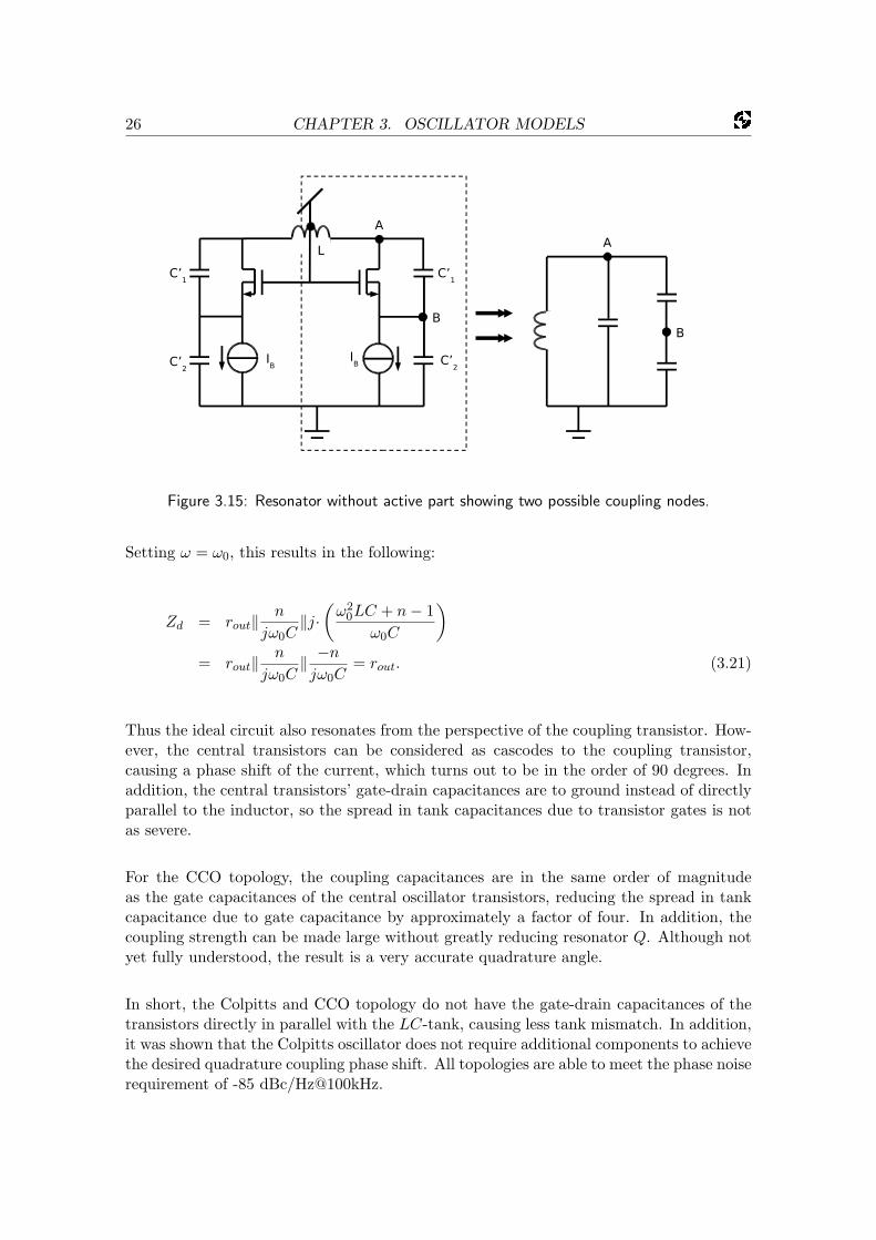
26 CHAPTER 3. OSCILLATOR MODELS
A
B
L
C2
C2
IB
IB
C1
C1
A
B
Figure 3.15: Resonator without active part showing two possible coupling nodes.
Setting ω = ω0, this results in the following:
Zd = rout‖n
jω0C‖j·
(ω2
0LC + n− 1ω0C
)= rout‖
n
jω0C‖ −n
jω0C= rout. (3.21)
Thus the ideal circuit also resonates from the perspective of the coupling transistor. How-ever, the central transistors can be considered as cascodes to the coupling transistor,causing a phase shift of the current, which turns out to be in the order of 90 degrees. Inaddition, the central transistors’ gate-drain capacitances are to ground instead of directlyparallel to the inductor, so the spread in tank capacitances due to transistor gates is notas severe.
For the CCO topology, the coupling capacitances are in the same order of magnitudeas the gate capacitances of the central oscillator transistors, reducing the spread in tankcapacitance due to gate capacitance by approximately a factor of four. In addition, thecoupling strength can be made large without greatly reducing resonator Q. Although notyet fully understood, the result is a very accurate quadrature angle.
In short, the Colpitts and CCO topology do not have the gate-drain capacitances of thetransistors directly in parallel with the LC-tank, causing less tank mismatch. In addition,it was shown that the Colpitts oscillator does not require additional components to achievethe desired quadrature coupling phase shift. All topologies are able to meet the phase noiserequirement of -85 dBc/Hz@100kHz.

Chapter 4
Buffer Design
The oscillators by themselves are relatively sensitive to parasitics. Varying load capaci-tances will cause changes in frequency, possibly upsetting the PLL, and low-Q loads willincrease the phase noise, or, even worse, prevent the oscillator from starting up altogether.All such effects must be eliminated and therefore a buffer needs to be an integral part ofthe oscillator, even more so, because if no inductors are used in the buffer, its power con-sumption may be quite large compared to the oscillator core itself. The most commonbuffer approach is to connect the gate of a MOSFET to the oscillator tank, which pro-vides a DC decoupling between the tank and the output. In this approach, the MOSFETcan be connected as either a common-source amplifier with gain or a source follower withno Miller capacitance multiplication from input to output. Both configurations will bedescribed with small-signal models in Section 4.1. Design and simulations of practicalbuffers will be presented in Section 4.2.
4.1 Small-Signal Buffer Models
Although in 65nm CMOS the transistors deviate strongly from ideal square-law andcurrent-source models, classical small-signal analysis still provides valuable insights intothe fundamental operation of analog circuits. At high frequencies, impedance transfor-mations help to simplify circuit analysis even further. The analysis of both the sourcefollower and the common-source amplifier, given below, are therefore conveniently simple.
4.1.1 Common-Source Amplifier
The circuit diagram and small-signal model for the capacitively loaded common-sourceamplifier are given in Figure 4.1.
In the small-signal model, the output is related to the input as follows.
Vout = −gm·Vin·(rout‖1
jωCL). (4.1)
27

28 CHAPTER 4. BUFFER DESIGN
Rd
CL
Rout
Vin·g
m
CL
Vout
Cgd
Vin
Vin
Vout
Figure 4.1: Schematic (left) and small-signal model (right) of a common-source buffer.
When worked out, this results in the following transfer function.
Vout
Vin= −gm·
rout
1 + jωroutCL= −gm·
rout − r2outjωCL
1 + r2outω
2C2L
. (4.2)
For an oscillator buffer, the phase shift is not very interesting. What is interesting, how-ever, is that the gain decreases with increasing load capacitance. This means also that theMiller multiplication factor decreases and thus the effective input capacitance decreaseswith increasing load capacitance. This is indeed what happens in simulations; as the 30fFload increases by a few percent, the oscillator frequency increases by several hundreds ofkHz.
Another interesting case is when |jωCLrout|1, easily achieved with large load capaci-tances at 10GHz. In that case, the current through the gate capacitance can be writtenas follows (gate capacitances to ground nodes are ignored for simplicity).
Iin = jωCgd·(Vin − Vout) = jωCgd·(Vin(1 +gm
jωCL)) = Vin·(jωCgd +
gm·Cgd
CL). (4.3)
For high frequencies, the transconductance and load capacitance therefore form a resis-tance in parallel with the input capacitance1, whose magnitude is given by
Vin
Iin=
1
jωCgd + gm·Cgd
CL
=1
jωCgd‖ CL
gm·Cgd, (4.4)
1By cross-coupling capacitors from input to output, a negative effective gate capacitance can even becreated and used to form a negative parallel input resistance that can sustain the entire oscillator. Thistechnique was already described in Section 3.2, but was actually inspired by considering the properties ofa CS buffer amplifier.
4.1. SMALL-SIGNAL BUFFER MODELS 29
or, equivalently (in series form)
=gm·Cgd
CL− jωCgd
g2m·C2
gd
C2L
+ ω2C2gd
=1
gm·Cgd
CL+ ω2CgdCL
gm
− jωg2
m·Cgd
C2L
+ ω2Cgd
. (4.5)
This directly reduces the Q of the tank and therefore the effect should be minimized.Intuitively, decreasing the load capacitance and decreasing the gate capacitance seem likelogical solutions. Up to a certain point, decreasing transconductance also increases theparallel resistance. Another option is to use a coupling capacitor, which transforms theresistance to Rtransformed = R·(1 + Cgd,eff/Ccoupling)2, but this also decreases the gain.In practice, the Miller capacitance is dominant, and –since it depends directly on the loadcapacitance– the oscillation frequency will depend on the load capacitance, making thebuffer provide poor shielding performance.
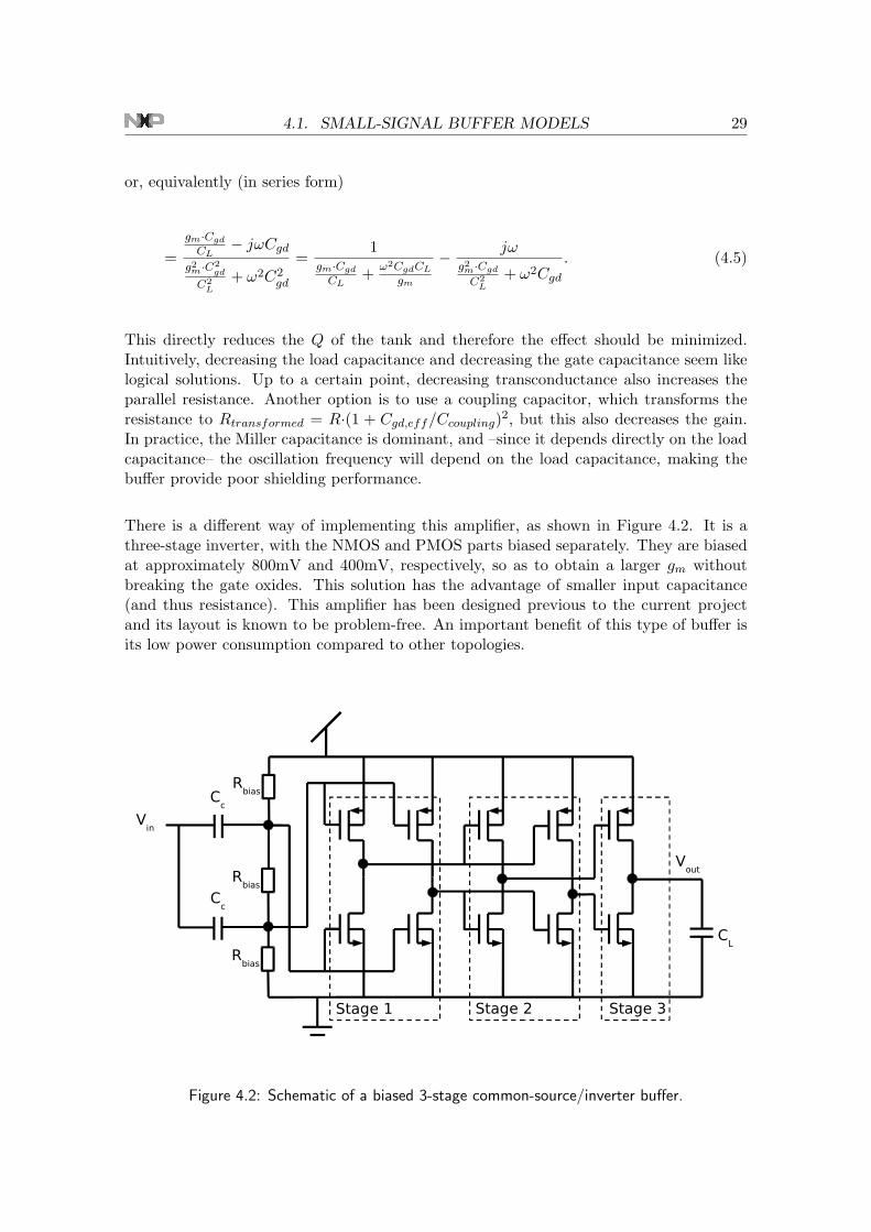
There is a different way of implementing this amplifier, as shown in Figure 4.2. It is athree-stage inverter, with the NMOS and PMOS parts biased separately. They are biasedat approximately 800mV and 400mV, respectively, so as to obtain a larger gm withoutbreaking the gate oxides. This solution has the advantage of smaller input capacitance(and thus resistance). This amplifier has been designed previous to the current projectand its layout is known to be problem-free. An important benefit of this type of buffer isits low power consumption compared to other topologies.
CL
Rbias
Cc
Vin
Cc
Rbias
Rbias
Vout
Stage 1 Stage 2 Stage 3
Figure 4.2: Schematic of a biased 3-stage common-source/inverter buffer.

30 CHAPTER 4. BUFFER DESIGN
4.1.2 Source Follower
As the oscillator swing is fairly large, even larger than the supply voltage, no gain largerthan one is required, so a source follower is also a good candidate for the buffer. As the gainis also non-inverting, no Miller multiplication takes place and no “strange” input resistanceis formed, other than the capacitively transformed output resistance. The circuit diagramand small-signal model for the capacitively loaded source follower are given in Figure 4.3.
Rs
CL
Vout
Vin
Rout
(Vin-V
out)·g
m
CL
Vout
Cgs
Vin
Figure 4.3: Schematic (left) and small-signal model (right) of a source follower buffer.
In the small-signal model, the output is related to the input as follows.
Vout = −gm·(rout‖1
jωCL)·(Vin − Vout)
⇐⇒ Vout
Vin=
gm·(rout‖ 1jωCL
)
1 + gm·(rout‖ 1jωCL
). (4.6)
It is clear that when gm is large enough, the gain approaches unity. In that case, alsothe gate-source capacitance becomes negligible, as no current flows through a capacitorbetween equipotential nodes. This in turn is very good for the tank Q, as the sourcefollower’s output resistance is not “felt” very strongly by the oscillator tank.
In reality, at the operating frequency of around 10GHz, gm is not automatically largeenough to avoid influence from the load on the frequency tuning. Therefore the sourcefollower’s input impedance is derived below (as for the CS stage, capacitances from the

4.2. PRACTICAL BUFFERS 31
gate to ground nodes are ignored for simplicity).
Iin = jωCgs(Vin − Vout) = jωCgs
(1− gm·rout
1 + jωCL·rout + gm·rout
)·Vin.
∴ Zin =Vin
Iin=
1 + jωCL·rout + gm·rout
jωCgs(1 + jωCL·rout). (4.7)
Clearly, for minimum input capacitance and minimum loading effects, rout should be verysmall and gm should be as large as possible.
4.2 Practical Buffers
For the oscillator running at 11.7GHz, it is possible to calculate what effect a change inbuffer input capacitance will have on the oscillation frequency. As the oscillation frequencydepends on the inverse square-root of the effective tank capacitance, a change in frequencycorresponding to one LSB of the varactor bank, so 1MHz, would be equivalent to a changein (single-ended) tank capacitance of 7.4aF, given a tank inductance of 1nH (500pH single-ended).
If a change in load capacitance of ±20% on 30fF is to have an effect on the frequency ofless than one varactor bank LSB, its impedance must be shielded by a factor of around1000. The question is how many source follower stages are required to achieve such ashielding, with reasonable values of gm≈0.01S, rout≈100Ω and Cgs≈30fF.
For this purpose, the source follower buffer’s input impedance may be rewritten as a series(negative) resistance and an input capacitance. The final expressions (resulting fromtedious derivation) are given below.
Rin =−gm·CL·r2
out
ω2CgsC2Lr2
out + Cgs. (4.8)
Cin =Cgs(1 + ω2C2
Lr2out)
1 + gm·rout + ω2C2Lr2
out
. (4.9)
To drive the load, gm·rout must be approximately equal to 1. As a quick check, accordingto (4.9), if gm·rout would be either zero or infinity, the load capacitance would have noinfluence on the input capacitance (an intuitively correct result). Filling in the reasonablevalues for all variables yields Cin = 15.22986fF for CL = 24fF and Cin = 15.55075fF forCL = 36fF. As this is a difference of 320aF, the single-stage buffer provides only slightly

32 CHAPTER 4. BUFFER DESIGN
more than the square-root of the required shielding factor. A second buffer stage couldsolve the problem.
However, a source follower provides no gain and the loss in amplitude, in combination withthe high power consumption (typically more than 40mW for the first stage alone), makesthe source follower quite unattractive. The biased three-stage inverter does not suffer fromsevere input resistance, provides enough shielding and typically consumes only 24mW ofpower in a differential quadrature configuration. Therefore, this (already available) typeof buffer was selected.
In conclusion, a biased 3-stage inverter buffer offers the required shielding between theoscillator and a variable load capacitance at the lowest power consumption. Therefore,the final buffers are implemented in this way.

Chapter 5
Inductor Design
Making physically large (and heavy!) inductors for e.g. audio applications has becomequite simple, as the size of the wire can generally be neglected with respect to the coilarea, parasitic capacitances are minimal, and many turns are generally wound, reducingedge effects.
Making planar inductors for operating frequencies of several GHz is unfortunately notso straightforward. Parasitic capacitances can easily decrease a coil’s internal resonancefrequency to unacceptable values and inductance values cannot be straightforwardly calcu-lated from the area that is enclosed by the coil, for still rather poorly understood reasons.
To help the circuit designer in choosing the appropriate inductor design, lumped modelsexist and, as of late, they can accurately describe how a certain planar inductor designbehaves [4]. A variation of the published LSIM inductor model was used to do circuitsimulations.
A constraint was placed on the area; the lateral dimensions should be in the order of100µm. The LSIM simulation tool indicated that for an octagonal 400pH inductor, theQ and resonance frequency would be optimal in the two-turn design with a track widthof 8µm and a spacing between the tracks of 10µm. In that case, Q = 26 at 10GHz andthe resonance frequency is around 40GHz. The resonance is chosen far from the operatingfrequency, because the effective inductance peaks just below the resonance frequency. Thiscan result in an uncontrollable influence on the tuning curve and other undesired effects,so it is preferable to have a more modest slope of the inductance around the operatingfrequency. For the chosen inductor, the plots of inductance and Q versus frequency areshown in Figure 5.1.
A smaller inductor is more sensitive to parasitics, especially interconnect resistance, butalso stray inductances. A 1µm long straight interconnect wire, for example, has a parasiticinductance of approximately 1pH, as given in [2, p. 140] by
L ≈ µ0l
2π
[ln
(2l
r
)− 0.75
]= (2×10⁻⁷)l
[ln
(2l
r
)− 0.75
], (5.1)
where l is the wire length and r is the radius, as the wire is assumed cylindrical. In practicethe expression is also useful for approximating non-cylindrical wires, as the length is themost important factor; the exact cross-sectional shape is actually not so important. Inanother project it has been observed that neglecting such effects can lead to a negativeshift of around 1GHz in the oscillating frequency of an LC-tank [6]. A more accurate
33

34 CHAPTER 5. INDUCTOR DESIGN
108
109
1010
1011
−5
−4
−3
−2
−1
0
1
2
3x 10
−9
Indu
ctan
ce (
H)
frequency (Hz)10
810
910
1010
11−300
−250
−200
−150
−100
−50
0
50
Q−
fact
or
frequency (Hz)
Figure 5.1: Inductance and Q versus frequency for an inductor with 100µm inner diameter.
formula (see Appendix D) reveals that the above formula is a little bit on the pessimisticside.
Even more detrimental is enclosing an area A with a wire loop, as approximated in [2,pp. 146–147] by
Lloop≈µ0
√πA . (5.2)
Apart from the self-inductance, enclosing areas with wire loops, even partially with largebends, can lead to mutual coupling to other parts of the circuit. This can be minimizedby so-called “Manhattan” layout structures, where horizontal and vertical lines are drawnin different metal layers and lines with opposite phase are run along each other overtheir entire length, i.e. further than some of the vias. As parasitic inductances cannot beextracted from the layout, one must be very careful not to make any current loops.
Finally, the IRR can depend to some extent on the mutual magnetic coupling betweenthe inductances of the two tanks [21], but this effect is, like the physical mechanismsdetermining inductance values of planar coils, poorly understood and will not be treatedin this report. In [21] it is observed that the proposed theory and the measurements didnot agree very well with each other.

Chapter 6
Frequency Tuning
Many process parameters have a certain tolerance, leading to differences between identi-cally designed circuits. The most important of these differences is the resulting variation inoscillation frequency. In this project, the idea is to compensate for production differences,which are expected to cause a frequency spread of ±5%, by means of a startup calibrationand to do small PLL adjustments using a finer frequency-tuning block.
The frequency adjustment is realized using digitally controlled variable capacitances (var-actors) in large arrays, so-called varactor banks. The startup calibration is done using acoarse varactor bank and the continuous fine-tuning is done using a fine varactor bank.
In Figure 6.1 the gate capacitance versus drive voltage is plotted for an NMOST. Thecapacitance is quite constant around 0V and for voltages larger than 1.2V. This can beexploited by switching the drive voltage digitally between the two regions and ensuringthat the AC swing is very small. In this way the capacitance is more linear and less proneto variation (for example, for non-constant supply voltage).
In principle, each varactor corresponds to a binary control bit, so subsequent varactorsdiffer in switchable capacitance by a factor two. For the fine varactor bank, purely binaryswitching could cause nonmonotonicity in the frequency tuning range, so a thermometercode is used for the most significant bits, limiting the maximum switched capacitance perelement to 8 LSB. In addition, the varactor capacitance does not scale linearly with areadue to edge effects. This is clearly visible when comparing Figure 6.1 and Figure 6.2. Fordecreasing varactor size, the amount of fixed capacitance also increases with respect tothe amount of variable capacitance.
For the Colpitts oscillator, the most natural way to implement the varactor is given inFigure 6.3. The capacitances C ′
1 and C ′2 can also be split up into four capacitances, with C3
being a variable capacitance, as shown in Figure 6.4. Note that in the actual oscillator, C4
would actually be a differential capacitor of half the specified capacitance (thus effectivelythe same). The latter solution will be studied first.
The input capacitance as seen from the tank is in that case
Cin = C1‖(C3 + (C2‖C4)) =C1C2C4 + C1C2C3 + C1C3C4
C1C2 + C1C4 + C2C3 + C2C4 + C3C4. (6.1)
The capacitive division ratio n at the node between C2 and C4 determines the phase noise[5]. For a variable C3, it cannot be kept constant, as follows from the expression given
35

36 CHAPTER 6. FREQUENCY TUNING
Figure 6.1: C–V curve of a 1µm2 varactor.
below.
n =C ′
1
C ′1 + C ′
2
=C1C2
C1C2 + C1C4 + C2C3 + C2C4 + C3C4. (6.2)
C3 only appears in the denominator, and its influence can only be minimized by choosingC1 very large, which means that C4 must be large enough to obtain a division ratio of 0.3.This in turn puts a lower limit on the variability of the term in C3C4.
To avoid the variation in n, it is possible also to vary C4, but this adds additional parasiticsto the circuit, which would probably introduce more phase noise and IRR degradation thanwould result from variations in n. In addition, it has appeared in simulations that 0.3 isnot always the optimum n for quadrature configurations; in fact, the optimum for n hasnot been properly characterized.
The differential capacitor C4 can be to ground as well, but this will affect the symmetry ofthe differential oscillator waveform. For this reason, it is also not preferable to do tuningwith this capacitance (as shown in Figure 6.3), as tuning capacitance is always to ground.However, as this method does not “downtransform” the negative series resistance of theoscillator to unacceptable values, it is in practice the only solution.
It is also possible to connect the tuning capacitance to the tank by means of an extraset of coupling capacitors. This makes the tuning capacitance more vulnerable to voltage

37
Figure 6.2: C–V curve of a minimum-size (120×60nm) varactor.
L
C2
C2
IB
IB
C1
C1
C3C
4
Figure 6.3: Schematic showing varactor connection.

38 CHAPTER 6. FREQUENCY TUNING
C1
L
C2
C2
IB
IB
C1
C1
C3
C2
C4
Figure 6.4: Schematic showing alternative varactor connection.
swings, as there is then no parallel capacitance to reduce the swing. This means that thecoupling capacitor must be very small and the resulting varactor bank would be, comparedto the chosen solution, quite enormous in chip area.
6.1 Tuning Linearity
The oscillator frequency is not linear with capacitance, but proportional to its inversesquare-root (contrary to the RC-oscillator, where the time constant is directly proportionalto C). For a small relative capacitance variation α, a linear approximation is valid, givenas
f0 =1
2πω0=
12π√
L· 1√
Cin=
12π√
L· 1√
C0(1 + α)
≈ 12π√
L· 1√
C0·(1− 1
2α). (6.3)
The tuning curve is not expected to be linear with the tuning word, but the above simplifi-cation is used to check if the tuning steps are in the correct order of magnitude. As a note,the step size should increase for higher frequencies, as the same change in capacitance αis then multiplied by a larger starting frequency. In practice this means that the tuningstep size varies from 500kHz at the bottom of the tuning range upward in the direction of1MHz, where the tuning range 11.36–12.17GHz is centered around 11.71GHz (determinedusing the scripts in Appendices E and F).

Chapter 7
Results
The topology choice was based on initial simulations, whose results are presented in Ta-ble 7.1. Phase noise was simulated using PSS and PNoise modes in Cadence. IRR wasestimated using only a very limited number (∼10-20) of Monte Carlo runs per design.Power consumption and FoM were calculated using PSS data. The 1/f3 corner is in allquadrature solutions simulated to be approximately 100kHz. Note that the center tap ofthe coil should be biased at 750mV for the CCO to perform optimally (output resistanceof this supply line has almost no influence due to the negligible current flow).
The Colpitts topology requires a higher supply voltage than the XCP topology to achievesufficiently low phase noise; this confirms the estimation based on (3.8) and (3.9).
Topology PRMS L(100kHz) FoM VDD 3σ IRR(mW) (dBc/Hz) (dB) (V) (dB)
Colpitts 50 -85 170 2 30X-Coupled Pair 20 -85 180 1.2 20
Crossed-Capacitor 100 -85 165 2 40
Table 7.1: Comparison of different oscillator topologies.
Simulated negative series resistances at the DC operating point are presented in Table 7.2.The resistance of the coil is 2.35Ω; dividing the magnitude of the negative series resistanceby this number gives the startup ratio. Note that in one of the cases the startup ratio istoo low. This is not necessarily a problem; it is considered a simulation inaccuracy (due toinaccurate models for TSMC devices) that in the fast process corner the gain is so muchlower. For the old NXP device models, the lowest startup gain was simulated to be 2.1,including parasitics. To get the startup ratio at this point, a cross-coupled pair was placedin parallel to the varactors, as described aptly in [10].
Condition −[email protected] Startup Ratio(Ω)
Cvar at 50%, no parasitic C 13.52 5.75
Table 7.2: Negative resistance and startup ratio of the final design at 27C across processcorners and tuning range (continued on next page).
39

40 CHAPTER 7. RESULTS
Condition −[email protected] Startup Ratio(Ω)
TYP corner 8.356 3.56Cvar at 50% slow corner 9.041 3.85
fast corner 5.493 2.34TYP corner 12.64 5.38
Cvar at 0% slow corner 12.73 5.42fast corner 10.24 4.36TYP corner 5.344 2.27
Cvar at 100% slow corner 6.405 2.73fast corner 2.082 0.886
Table 7.2: Negative resistance and startup ratio of the final design at 27C across processcorners and tuning range.
This leads to the final schematic given with dimensions in Figure 7.1 (I part) and Figure 7.2(Q part). The I+, I−, Q+ and Q− nodes are each buffered by a buffer, shown with dimen-sioning in Figure 7.3. The accompanying digital varactor implementation is not shown.The varactors are from the sources of the central transistors to ground, the coarse bankconsisting of 0.76µm×0.76µm varactors and the fine bank consisting of 0.14µm×0.14µmvaractors. Each bank is made up of 63 elements (equivalent to 6 bits in a binary controlscheme), with 7 elements of 8LSB, 1 element of 4LSB and 3 elements of 1LSB. Thus, noelements larger than 8LSB need to be switched, in order to prevent nonmonotonicity dueto mismatch.
The schematics and simulations of the mixers and the following buffers on the test chipare not presented, as these circuits were not designed by the author.
Phase noise without buffer is simulated at -83dBc/Hz@100kHz, with the oscillator am-plitude at 3.8Vpp. This implementation typically consumes 70mWrms of power from the2V supply (working in the range of 1.6-2.0V). The buffers, connected across the coils,consume an additional 24mWrms from the 1.2V supply, reducing the oscillator swing bya factor of approximately 4. The varactor is split into a fine and a coarse bank, withthe minimum tuning step estimated at 500kHz. The total chip area of one quadratureoscillator including buffers is 210µm×480µm≈0.1mm2.
Simulations with the (unfortunately inaccurate) TSMC device models are shown in Fig-ures 7.4–7.11. High oscillator frequencies for some simulations are related to the omissionof parasitic capacitances. Layouts of the oscillator and the test chip are shown in Fig-ure 7.12 and Figure 7.13, respectively.

41
L
285fF
Cvar
I+ I
QQ+
200
2k 2k
200
Cvar
285fF
48/0.0648/0.06
36/0.436/0.4
32/
0.12
32/
0.12
Figure 7.1: Final Colpitts schematic I part (varactors not shown).
L
285fF
Cvar
I+I
QQ+
200
2k 2k
200
Cvar
285fF
48/0.0648/0.06
36/0.436/0.4
32/
0.12
32/
0.12
Figure 7.2: Final Colpitts schematic Q part (varactors not shown).

42 CHAPTER 7. RESULTS
10k
10fFVin
10fF
10k
10k
Vout
10/
0.06
10/
0.06
10/
0.06
10/
0.06
6/
0.06
6/
0.06
6/
0.06
16/0.06
12/
0.06
14/
0.06
Figure 7.3: Final schematic of the biased 3-stage common-source/inverter buffer.
Figure 7.4: Phase noise plot generated using TSMC models and equivalent ideal capacitorsinstead of the varactor banks.

43
Figure 7.5: PSS waveforms of the four oscillator outputs in the presence of 2fF tank mismatch.
Figure 7.6: PSS waveforms of the four buffer outputs in the presence of 2fF tank mismatch.
44 CHAPTER 7. RESULTS
Figure 7.7: Oscillation frequency versus load capacitance at the buffer output. Simulationnoise dominates over any systematic change in frequency.
Figure 7.8: Tuning curve for the coarse varactor bank. The sudden step and the nonmono-tonicity in the region of high capacitance are known to be simulation artifacts.

45
Figure 7.9: Tuning curve for the fine varactor bank. The sudden step is a known simulationartifact.
Figure 7.10: Monte Carlo histogram showing variation in oscillation frequency (left) andquadrature angle (right).

46 CHAPTER 7. RESULTS
Figure 7.11: Monte Carlo histogram showing variation in oscillation frequency (left) andquadrature angle (right) in the presence of an additional 2fF tank mismatch.
Figure 7.12: Final layout of the QDCO including buffers.

47
Figure 7.13: Final layout of the test chip.

Chapter 8
Benchmarking
The circuits that form the reference for this QDCO are given in [16]. In [27] a CMOS VCOof higher frequency is presented, but the quadrature accuracy, strangely, is measured onan 8.5GHz scaled VCO, and only the result for a single IRR measurement is given. Theauthor believes that the matching problems and parasitic mutual coupling will increase athigher frequency, making the quadrature accuracy for this concept unacceptable. In [28]a 32GHz QVCO in an SiGe process is presented1, which is actually the only chip that canmatch the performance of the DCO designed in this report, uses five times more powerand needs a tremendous supply voltage of 5V (which is bad for integrability). Finally, a16GHz QVCO in SiGe (running on a reasonable 2.7V supply) is presented in [23]. Its phasenoise performance is excellent, but the quadrature accuracy of 6 degrees RMS (equivalentto a 3-σ spread of 18 degrees, see [29]) is vehemently insufficient. Curiously, the authorsconsider the matching of tail current sources to be crucial for the quadrature accuracy.
The current state-of the art in CMOS is an IRR of more than 40dB with a FoM of around185. There are several reasons why these specifications are difficult to achieve at 11.7GHz.
First of all, injection locking is not an option at 11.7GHz with the desired phase noise,as a locking current source severely degrades phase noise performance. Also, at higherfrequency the dI/dt in the coils is larger, increasing the effect of mutual coupling (which isknown to have a detrimental effect on the IRR, see [21]). Because the oscillator tanks arevery strongly coupled, however, this might not be as dominant a problem in the currentoscillator as would appear from literature.
Finally, it is not customary to compensate so strongly for tank mismatches, as most CMOSquadrature oscillators are designed for lower frequencies (the comparison in [16] does notinclude oscillators above 5GHz). As the capacitor mismatch scales with 1/
√WL and
therefore increases with decreasing capacitance (under the condition of minimal parasitics),the achievable IRR for a certain coupling type becomes a function of frequency and itbecomes more difficult to achieve a certain IRR as frequency increases.
In this context, it becomes desirable to include the relationship between IRR and oper-ating frequency as a separate term into the FoM. The relative 3-σ mismatch error scalesapproximately with the inverse square-root of the capacitance, so scales linearly with fre-quency. Therefore the relative frequency mismatch scales with the square-root of thefrequency. To a first order, the quadrature coupling strength scales with the square of
1It appears that in equation (1) of the article, the authors forgot to square the capacitances.
49
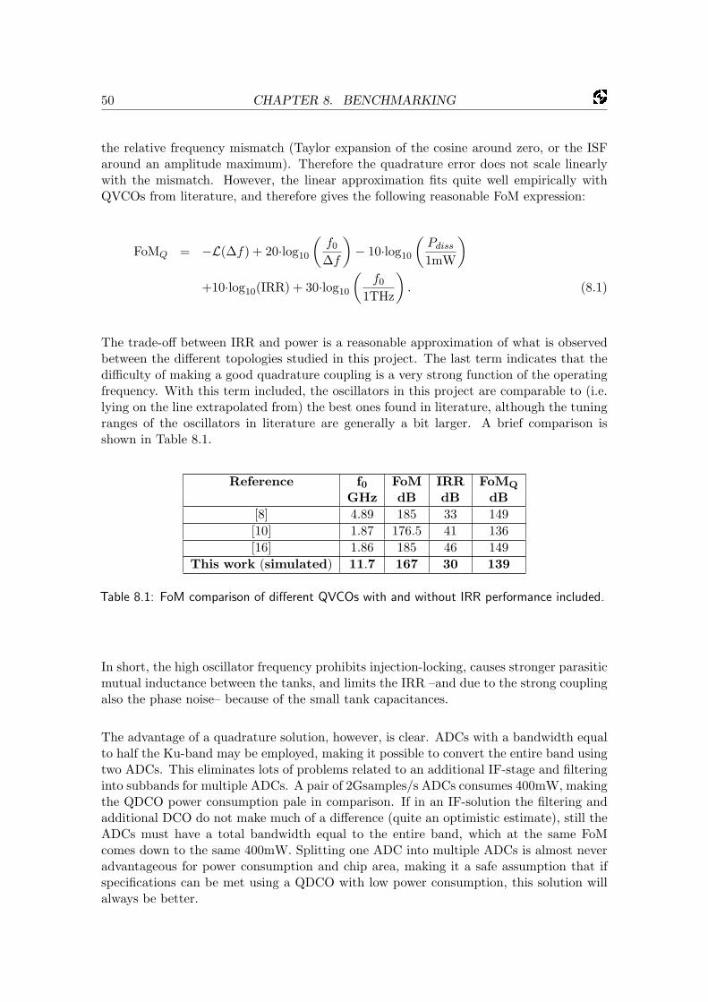
50 CHAPTER 8. BENCHMARKING
the relative frequency mismatch (Taylor expansion of the cosine around zero, or the ISFaround an amplitude maximum). Therefore the quadrature error does not scale linearlywith the mismatch. However, the linear approximation fits quite well empirically withQVCOs from literature, and therefore gives the following reasonable FoM expression:
FoMQ = −L(∆f) + 20·log10
(f0
∆f
)− 10·log10
(Pdiss
1mW
)+10·log10(IRR) + 30·log10
(f0
1THz
). (8.1)
The trade-off between IRR and power is a reasonable approximation of what is observedbetween the different topologies studied in this project. The last term indicates that thedifficulty of making a good quadrature coupling is a very strong function of the operatingfrequency. With this term included, the oscillators in this project are comparable to (i.e.lying on the line extrapolated from) the best ones found in literature, although the tuningranges of the oscillators in literature are generally a bit larger. A brief comparison isshown in Table 8.1.
Reference f0 FoM IRR FoMQ
GHz dB dB dB[8] 4.89 185 33 149[10] 1.87 176.5 41 136[16] 1.86 185 46 149
This work (simulated) 11.7 167 30 139
Table 8.1: FoM comparison of different QVCOs with and without IRR performance included.
In short, the high oscillator frequency prohibits injection-locking, causes stronger parasiticmutual inductance between the tanks, and limits the IRR –and due to the strong couplingalso the phase noise– because of the small tank capacitances.
The advantage of a quadrature solution, however, is clear. ADCs with a bandwidth equalto half the Ku-band may be employed, making it possible to convert the entire band usingtwo ADCs. This eliminates lots of problems related to an additional IF-stage and filteringinto subbands for multiple ADCs. A pair of 2Gsamples/s ADCs consumes 400mW, makingthe QDCO power consumption pale in comparison. If in an IF-solution the filtering andadditional DCO do not make much of a difference (quite an optimistic estimate), still theADCs must have a total bandwidth equal to the entire band, which at the same FoMcomes down to the same 400mW. Splitting one ADC into multiple ADCs is almost neveradvantageous for power consumption and chip area, making it a safe assumption that ifspecifications can be met using a QDCO with low power consumption, this solution willalways be better.
Chapter 9
Conclusion
After reviewing various ways of generating quadrature baseband signals in a Ku-bandsatellite receiver, it is concluded that a quadrature LC-oscillator, operating at 11.7GHzwith an IRR of 30dB and a phase noise of -85dBc/Hz@100kHz, is the best means to thisend. Three quadrature oscillator-topologies were studied, among which the novel CCOtopology, which seems very suitable for future CMOS oscillator designs, and the moretraditional XCP and Colpitts topologies.
Of the three topologies studied, both the Colpitts topology and the CCO topology meet theestimated IRR requirement of 30dB, with the Colpitts showing a better FoM and a widertuning range, whereas the CCO topology can achieve a better quadrature accuracy. Thepoor IRR performance of the XCP topology is attributed to the poor matching propertiesof gate-drain capacitances. The Colpitts topology is able to meet phase noise specificationsdue to its ability to run at a high supply voltage of 2V.
After analysis, it is concluded that for phase noise performance, not only the coupling angleof first-harmonic coupling, but also the strength of the coupling have a clear optimum.It is further concluded that the optimum coupling strength w.r.t. phase noise cannot bedirectly achieved in the presence of realistic tank mismatches, as the quadrature couplingmust then be much stronger.
A frequency tuning mechanism, designed for a digital PLL and capable of compensatingfor process spread, has been added to the oscillator, including three-stage-inverter buffers.The complete oscillator core is simulated to consume approximately 70mWrms at a supplyvoltage of 2V, with the buffers consuming an additional 24mWrms. This is reasonably inline with other published quadrature oscillators.
A chip layout of the concept has been made, with two oscillators of which one has its bufferoutput directly connected to the bondpad, and the other is first passed through a mixerstage, such that the quadrature accuracy can be measured properly. Once some samplesare produced, their phase noise spectra and quadrature accuracy still need to be measured.This allows simulation inaccuracies to be identified, such that a better oscillator may bedesigned.
51


References
[1] Thomas H. Lee, The Design of CMOS Radio-Frequency Integrated Circuits, SecondEdition, Cambridge University Press, New York, 2004, ISBN 0-521-83539-9.
[2] Thomas H. Lee, Planar Microwave Engineering, Cambridge University Press, Cam-bridge, 2004, ISBN 0-521-83526-7.
[3] Ali Hajimiri and Thomas H. Lee, “A General Theory of Phase Noise in Electrical Os-cillators,” IEEE Journal of Solid-State Circuits, vol. 33, no. 2, pp. 179–194, Feb. 1998.
[4] Luuk F. Tiemeijer et al., “Physics-Based Wideband Predictive Compact Model forInductors With High Amounts of Dummy Metal Fill,” IEEE Transactions on Mi-crowave Theory and Techniques, vol. 54, no. 8, pp. 3378–3386, Aug. 2006.
[5] Pietro Andreani et al., “A Study of Phase Noise in Colpitts and LC-Tank CMOSOscillators,” IEEE Journal of Solid-State Circuits, vol. 40, no. 5, pp. 1107–1118,May 2005.
[6] Edwin van der Heijden and Cicero S. Vaucher, “Low Phase Noise, Low Power Ka-Band (18GHz) LC-VCOs in QUBiC4X,” NXP Semiconductors Technical Note NXP-R-TN 2007/00079, NXP Restricted, Mar. 2007.
[7] Edwin van der Heijden, private communications.
[8] Sander L.J. Gierkink et al., “A Low-Phase-Noise 5-GHz CMOS Quadrature VCOUsing Superharmonic Coupling,” IEEE Journal of Solid-State Circuits, vol. 38, no. 7,pp. 1148–1154, July 2003.
[9] Pepijn van de Ven et al., “An optimally coupled 5 GHz quadrature LC oscillator,”Symposium on VLSI Circuits Dig. of Tech. Papers, pp. 115–118, 2001.
[10] Roberto Aparicio and Ali Hajimiri, “A Noise-Shifting Differential Colpitts VCO,”IEEE Journal of Solid-State Circuits, vol. 37, no. 12, pp. 1728–1736, Dec. 2002.
[11] Alper Demir et al., “Phase Noise in Oscillators: A Unifying Theory and Numeri-cal Methods for Characterization,” IEEE Transactions on Circuits and Systems—I:Fundamental Theory and Applications, vol. 47, no. 5, pp. 655–674, May 2000.
[12] Alper Demir, “Computing Timing Jitter From Phase Noise Spectra for Oscillatorsand Phase-Locked Loops With White and 1/f Noise,” IEEE Transactions on Circuitsand Systems—I: Regular Papers, vol. 53, no. 9, pp. 1869–1884, Sep. 2006.
[13] Piet Vanassche et al., “On the Difference Between Two Widely Publicized Methodsfor Analyzing Oscillator Phase Behavior,” in Proc. ACM/IEEE Int. Conf. Comput.-Aided Design, pp. 229–233, Nov. 2002.
53

54 REFERENCES
[14] Fergal O’Doherty and James P. Gleeson, “Phase Diffusion Coefficient for Oscilla-tors Perturbed by Colored Noise,” IEEE Transactions on Circuits and Systems—II:Express Briefs, vol. 54, no. 5, pp. 435–439, May 2007.
[15] Asad A. Abidi, “High-Frequency Noise Measurements on FET’s with Small Dimen-sions,” IEEE Transactions on Electron Devices, vol. ED-33, no. 11, pp. 1801–1805,Nov. 1986.
[16] Andrea Mazzanti and Francesco Svelto, “A 1.8-GHz Injection-Locked QuadratureCMOS VCO With Low Phase Noise and High Phase Accuracy,” IEEE Transactionson Circuits and Systems—I: Regular Papers, vol. 53, no. 3, pp. 554–560, Mar. 2006.
[17] Behzad Razavi, RF microelectronics, Prentice Hall, Upper Saddle River, 1998, ISBN0-13-887571-5.
[18] John Ardizzoni, “High-Speed Time-Domain Measurements — Practical Tips for Im-provement,” Analog Dialogue, vol. 41, no. 1, pp. 13–18, Jan. 2007.
[19] Domine M.W. Leenaerts et al., “A 15-mW Fully Integrated I/Q Synthesizer forBluetooth in 0.18-µm CMOS,” IEEE Journal of Solid-State Circuits, vol. 38, no. 7,pp. 1155–1162, July 2003.
[20] Pietro Andreani, “A Time-Variant Analysis of the 1/f2 Phase Noise in CMOS ParallelLC-Tank Quadrature Oscillators,” IEEE Transactions on Circuits and Systems—I:Regular Papers, vol. 53, no. 8, pp. 1749–1760, Aug. 2006.
[21] Andrea Mazzanti et al., “On the Amplitude and Phase Errors of Quadrature LC-TankCMOS Oscillators,” IEEE Journal of Solid-State Circuits, vol. 41, no. 6, pp. 1305–1313, June 2006.
[22] Xiaoyong Li, Low Noise Design Techniques for Radio Frequency Integrated Circuits,Ph.D. Thesis, University of Washington, 2004.
[23] Aly Ismail and Asad A. Abidi, “A 3.1- to 8.2-GHz Zero-IF Receiver and Direct Fre-quency Synthesizer in 0.18µm SiGe BiCMOS for Mode-2 MB-OFDM UWB Com-munication,” IEEE Journal of Solid-State Circuits, vol. 40, no. 12, pp. 2573–2582,Dec. 2005.
[24] Ahmad Mirzaei et al., “The Quadrature LC Oscillator: A Complete Portrait Basedon Injection Locking,” IEEE Journal of Solid-State Circuits, vol. 42, no. 9, pp. 1916–1932, Sep. 2007.
[25] Sherif H. Galal et al., “RC Sequence Asymmetric Polyphase Networks for RF Inte-grated Transceivers,” IEEE Transactions on Circuits and Systems—II: Analog andDigital Signal Processing, vol. 47, no. 1, pp. 18–27, Jan. 2000.
[26] Farbod Behbahani et al., “CMOS Mixers and Polyphase Filters for Large Image Re-jection,” IEEE Journal of Solid-State Circuits, vol. 36, no. 6, pp. 873–887, June 2001.
[27] Alan W.L. Ng and Howard C. Luong, “A 1V 17GHz 5mW Quadrature CMOSVCO based on Transformer Coupling,” ISSCC Dig. Of Tech. Papers, pp. 711-720,Feb. 2006.

REFERENCES 55
[28] W.L. Chan et al., “A 32GHz Quadrature LC-VCO in 0.25µm SiGe BiCMOS Tech-nology,” ISSCC Dig. Of Tech. Papers, pp. 538-539, Feb. 2005.
[29] Wikipedia Article, “Standard deviation,” at the time of writing available from:http://en.wikipedia.org/wiki/Standard deviation
[30] Jason Hildebrand, “Differentiating Arctan(x),” at the time of writing available from:http://www.opensky.ca/∼jdhildeb/arctan/arctan diff.html
[31] MathPages Article, “How Leibniz Might Have Anticipated Euler,” at the time ofwriting available from:http://www.mathpages.com/home/kmath477.htm

Appendix A
Derivation ISF of LC-Oscillator
In the 1998 paper by Hajimiri and Lee [3], the shape of the ISF of an LC-oscillator issimply given without derivation. The derivation for a lossless parallel LC-tank (a closeapproximation of reality) is given below, uncovering an inaccuracy in the original paper.
A.1 Definitions
For a parallel LC-tank, due to the choice of reference directions for the voltage and thecurrent, we must reverse the sign of one of the component equations. This is done asfollows. The choice of the minus sign eases the derivation significantly.
V = −jωLI =−jI
Cω. (A.1)
We will use the time domain, so it is useful to define the phase relationship between voltageand current as follows.
V = V0·sinω0·t. (A.2)I = I0·cos ω0·t. (A.3)
We define, again for simplicity, the tank energy as
E0 =12CV 2 +
12LI2 =
12CV 2
0 sin2ω0·t +12LI2
0cos2ω0·t. (A.4)
Note also that
E0 =12CV 2
0 =12LI2
0 (A.5)
and
qmax = C·V0 =2E0
V0. (A.6)
This allows us to define the ratio of the two tank amplitudes as follows.
V0
I0=
√L
C. (A.7)
57

58 APPENDIX A. DERIVATION ISF OF LC-OSCILLATOR
A.2 Derivation
If we now consider only one oscillation period, we may simply substitute the phase angleθ for ω0·t. The phase angle may always be derived from the instantaneous voltage andcurrent.
V
I=
V0·sin θ
I0·cos θ=
V0
I0·tan θ =
√L
C·tan θ
⇐⇒ θ = arctan(
V
I·√
C
L
)(A.8)
Its instantaneous sensitivity, normalized to a unity voltage change1, is simply the derivativewith respect to the voltage, which is worked out below (using the fun-to-derive derivativeof arctan(x) [30] [31]).
dθ
dV=
d
dV
(arctan
(V
I·√
C
L
))=
11 + V 2
I2 ·CL·1I·√
C
L
=I
LI2 + CV 2·√
LC =V0·C· cos θ
2·E0. (A.9)
The ISF is the sensitivity normalized to a unity current impulse2 or dθ/dq, so we are notquite there yet. The voltage step amplitude is proportional to 1/C times the injectedcharge (interestingly, the inductor has nothing to do with the charge injection), yielding,after some substitutions for V0, the following expression, which is not dimensionless, as theone in the Hajimiri & Lee paper, but has the unit radians per Coulomb (phase change perdisturbance charge). The subscript F denotes the formal correctness; in the next sectionit is shown that the original definition is formally incorrect.
ΓF (θ) = ω0·√
L
2·E0· cos θ =
cos θ
qmax. (A.10)
From this, it follows that the sensitivity of the phase depends on the cosine of the phase,decreases with the square-root of the tank energy (in other words, linearly with eithercurrent or voltage amplitude), and increases linearly with frequency. Once frequencyand tank energy are chosen fixed, the ISF scales with the square-root of the inductance,i.e. a smaller inductance yields also a smaller ISF. Intuitively, a larger capacitor is lesssensitive to noise currents, as the relative charge noise is then smaller. This intuition isnow confirmed.
1For large changes in θ, one must actually do a path integral over dθ to obtain accurate results.2Normalized, because a unity current impulse is a Coulomb of charge, which is rediculously enormous!
In the paper by Hajimiri and Lee [3], the ISF is defined as the sensitivity to the actual impulse, ignoringthe fact that a path integral must be done for large variations in θ. Intuitively, adding a current impulseof infinite magnitude leads to an infinite V/I ratio, or an amplitude maximum, and not simply the phaseat the injection start plus the ISF at the injection start multiplied by the impulse magnitude.
A.3. CORRECTION FOR LARGE IMPULSES 59
A.3 Correction for Large Impulses
For large current impulses of magnitude K, applied at starting voltage V1 and leading tovoltage V2, we have
V2 − V1 =1C·∫ 0+
0−K·δ(t)dt =
K
C. (A.11)
Deriving the phase change involves doing a rather simple integral.
θ2 − θ1 =∫ V2
V1
dθ
dV·dV =
∫ θ(V2)
θ(V1)dθ
= arctan(
V1 + K/C
I·√
C
L
)− arctan
(V1
I·√
C
L
). (A.12)
This correction has no practical value, because the linear approximation made by directlyconvolving the ISF with the noise is generally very good and much faster to compute, butit clarifies the already very difficult phase noise analysis by a small amount.
In [3] it is not clear that an approximation of the path integral is made (in fact, this can bequite confusing). Because the phase change depends nonlinearly on the impulse magnitudeK, the system is nonlinear and it is formally incorrect to define an impulse response. Adefinition in infinitely small changes, however, such as dθ/dq, does not assume linearity ofthe impulse response and is therefore formally correct.

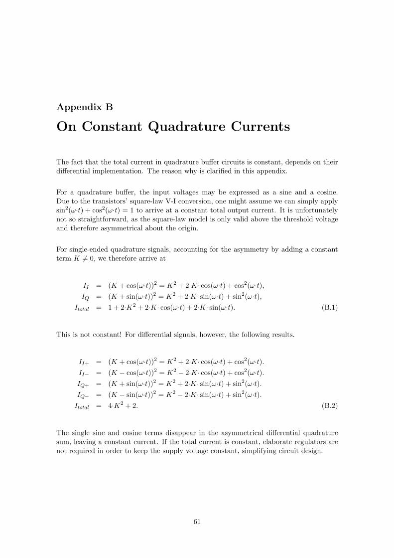
Appendix B
On Constant Quadrature Currents
The fact that the total current in quadrature buffer circuits is constant, depends on theirdifferential implementation. The reason why is clarified in this appendix.
For a quadrature buffer, the input voltages may be expressed as a sine and a cosine.Due to the transistors’ square-law V-I conversion, one might assume we can simply applysin2(ω·t) + cos2(ω·t) = 1 to arrive at a constant total output current. It is unfortunatelynot so straightforward, as the square-law model is only valid above the threshold voltageand therefore asymmetrical about the origin.
For single-ended quadrature signals, accounting for the asymmetry by adding a constantterm K 6= 0, we therefore arrive at
II = (K + cos(ω·t))2 = K2 + 2·K· cos(ω·t) + cos2(ω·t),IQ = (K + sin(ω·t))2 = K2 + 2·K· sin(ω·t) + sin2(ω·t),
Itotal = 1 + 2·K2 + 2·K· cos(ω·t) + 2·K· sin(ω·t). (B.1)
This is not constant! For differential signals, however, the following results.
II+ = (K + cos(ω·t))2 = K2 + 2·K· cos(ω·t) + cos2(ω·t).II− = (K − cos(ω·t))2 = K2 − 2·K· cos(ω·t) + cos2(ω·t).IQ+ = (K + sin(ω·t))2 = K2 + 2·K· sin(ω·t) + sin2(ω·t).IQ− = (K − sin(ω·t))2 = K2 − 2·K· sin(ω·t) + sin2(ω·t).
Itotal = 4·K2 + 2. (B.2)
The single sine and cosine terms disappear in the asymmetrical differential quadraturesum, leaving a constant current. If the total current is constant, elaborate regulators arenot required in order to keep the supply voltage constant, simplifying circuit design.
61


Appendix C
CCO and Process Scaling
There are several trends in the downscaling of CMOS processes, and it is anticipated thatthe CCO topology is very fit to deal with these changes.
Firstly, minimum transistor length will decrease. This is good news, as the same gaincan be made with a smaller gate capacitance, enlarging the currently problematic tuningrange of the CCO. Also, less gate capacitance means less variation in tank capacitancedue to process spread, because the fringe capacitors vary much less in capacitance thando gate capacitances.
Secondly, especially for the anticipated 32nm FinFET transistors, making low-ohmicsource and drain contacts is becoming problematic. This is not such a big deal in theCCO, as the channel is completely decoupled from the LC-tank.
As frequency gets higher (60GHz CMOS projects are already underway), the CCO hasan additional advantage. In (3.11) the term with the output resistance vanishes for highfrequencies. This also explains why the CCO is the only topology for which the phasenoise does not increase with frequency; it also means that the CCO should typically beapplied at frequencies near the fT of the process.
Finally, there is a trend that mismatch becomes worse as the device sizes continue toshrink. As the CCO in quadrature configuration shows much better IRR performancethan any other topology, this indicates less sensitivity to mismatch.
In conclusion, the CCO topology and its study may be worth keeping for future reference,especially since its power-no-object phase noise performance is superior in both singleand quadrature configurations. In case the structure is used in a future system, thedesigner may have a closer look at the start-up conditions, as simulations suggest a differentoptimum ratio of negative to positive resistance than for more traditional topologies,probably due to different gate biasing and different large-signal (describing function) gain.
63


Appendix D
Estimation of Parasitic Inductance
Below are some formulæ [7] that give first-order approximations of the behavior of straighton-chip interconnect lines:
l = v·t, (D.1)
v =c√
εr, (D.2)
t =√
LC , (D.3)
Z0 =
√L
C. (D.4)
These lead to the following expressions for the inductance and characteristic impedanceof the line:
L =l2εr
c2C, (D.5)
Z0 =l√
εr
c·C. (D.6)
In all cases, c≈3·108m/s and, for the CMOS process used in this project, εr≈4. Theexpression for the parasitic inductance is known to give an accurate (within a few percent)first-order approximation [7].
The capacitance scales approximately linearly with length, leading to an almost lineardependence of the inductance on the wire length, which turns out to be approximately60pH/100µm for a 0.4µm wide line with Metal 4 as the lowest layer. This is only a factor0.6 compared to the formula given for bondwires in [2, p. 140].
The characteristic impedance of the line is 95Ω.
65


Appendix E
Fine Tuning Script Colpitts QDCO
1 ;%%%%%%%%%%%%%%%%%%%%%%%%%%%%%%%%%%%%%%%%%%%%%%%%%%%%%%%%%%%%%%%%%%%
2 ;%%% Simulation of QDCO tuning curves %%%
3 ;%%% Frank Leong , May 2007 %%%
4 ;%%%%%%%%%%%%%%%%%%%%%%%%%%%%%%%%%%%%%%%%%%%%%%%%%%%%%%%%%%%%%%%%%%%
5 ; np_tuningCharacteristic( list( 0) list(0 4 8 31 63) list( 27 ) list( 1 )
)
6 ; np_tuningCharacteristic( list( 0) list(0 1 2 3 4 5 6 7 8 9 10 11 12 13 14
15 16 17 18 19 20 21 22 23 24 25 26 27 28 29 30 31 32 33 34 35 36 37
38 39 40 41 42 43 44 45 46 47 48 49 50 51 52 53 54 55 56 57 58 59 60 61
62 63) list( 27 ) list( 1 ) )
7 ; load( "./ tune_frank4.ocn")
89
10 procedure( run_VCO_analysis( coarse fine tempval corner )
1112 simulator( ’spectre )
1314 design( "/home/nlv15336/paulg/simulation/pss_tune_colpitts2/spectre/
schematic/netlist/netlist ")
15 resultsDir( "/home/nlv15336/paulg/simulation/pss_tune_colpitts2/spectre/
schematic/psf" )
161718 if( corner ==0
19 then
20 modelFile( ’("/home/nlv15336/Workareas4/UTC065_nlv15336/b6Ra1/
include_snsp.scs" "" ) )
21 )
2223 if( corner ==1
24 then
25 modelFile( ’("/home/nlv15336/Workareas4/UTC065_nlv15336/b6Ra1/
include_nominal.scs" "" ) )
26 )
2728 if( corner ==2
29 then
30 modelFile( ’("/home/nlv15336/Workareas4/UTC065_nlv15336/b6Ra1/
include_fpfn.scs" "" ) )
31 )
3233 ;analysis(’pnoise ?relharmnum "1" ?start "1e3" ?stop "1e9"
34 ; ?maxsideband "5" ?p "/n075" ?n "/gnd!" ?oprobe ""
35 ; ?iprobe "" ?refsideband "" )
36 analysis(’pss ?fund "8G" ?harms "5" ?errpreset "conservative"
37 ?tstab "5n" ?saveinit "no" ?p "/n075" ?n "/gnd!"
38 ?maxstep "1p" ?method "gear2only" ?tstabmethod "gear2only
" )
39 desVar( "clsim5" 3.5371p )
67

68 APPENDIX E. FINE TUNING SCRIPT COLPITTS QDCO
40 desVar( "clsim1" 37.2286f )
41 desVar( "clsim2" 300.679f )
42 desVar( "clsim3" -10.0821f )
43 desVar( "clsim4" 5.51919f )
44 desVar( "llsim4" 80.2779p )
45 desVar( "llsim5" -129.703p )
46 desVar( "llsim2" 7.16401p )
47 desVar( "llsim6" -0.495176p )
48 desVar( "llsim8" -5.54881p )
49 desVar( "llsim3" 18.1179p )
50 desVar( "llsim1" 430.961p )
51 desVar( "llsim7" -1.25231p )
52 desVar( "rlsim2" 2.98229 )
53 desVar( "rlsim4" 1.69803 )
54 desVar( "rlsim1" 6.37948 )
55 desVar( "rlsim3" 1.51149 )
56 desVar( "rlsim5" 1.56008 )
57 desVar( "rlsim6" -0.415667 )
58 desVar( "rlsim8" 0.483 )
59 desVar( "rlsim9" 707.547 )
60 desVar( "rlsim7" 1.955 )
61 ;desVar( "fine" fine )
62 ;desVar( "coarse" coarse )
6364 if( mod(fine 4)==0
65 then
66 desVar( "thrm1_0" 0 )
67 desVar( "thrm1_1" 0 )
68 desVar( "thrm1_2" 0 )
69 )
70 if( mod(fine 4)==1
71 then
72 desVar( "thrm1_0" 1.2 )
73 desVar( "thrm1_1" 0 )
74 desVar( "thrm1_2" 0 )
75 )
76 if( mod(fine 4)==2
77 then
78 desVar( "thrm1_0" 1.2 )
79 desVar( "thrm1_1" 1.2 )
80 desVar( "thrm1_2" 0 )
81 )
82 if( mod(fine 4)==3
83 then
84 desVar( "thrm1_0" 1.2 )
85 desVar( "thrm1_1" 1.2 )
86 desVar( "thrm1_2" 1.2 )
87 )
88 if( mod(fine 8) >=4
89 then
90 desVar( "thrm4" 1.2 )
91 else
92 desVar( "thrm4" 0 )
93 )
94 if( fine >=8
95 then
96 desVar( "thrm8_0" 1.2 )
97 else

69
98 desVar( "thrm8_0" 0 )
99 )
100 if( fine >=16
101 then
102 desVar( "thrm8_1" 1.2 )
103 else
104 desVar( "thrm8_1" 0 )
105 )
106 if( fine >=24
107 then
108 desVar( "thrm8_2" 1.2 )
109 else
110 desVar( "thrm8_2" 0 )
111 )
112 if( fine >=36
113 then
114 desVar( "thrm8_3" 1.2 )
115 else
116 desVar( "thrm8_3" 0 )
117 )
118 if( fine >=40
119 then
120 desVar( "thrm8_4" 1.2 )
121 else
122 desVar( "thrm8_4" 0 )
123 )
124 if( fine >=48
125 then
126 desVar( "thrm8_5" 1.2 )
127 else
128 desVar( "thrm8_5" 0 )
129 )
130 if( fine >=56
131 then
132 desVar( "thrm8_6" 1.2 )
133 else
134 desVar( "thrm8_6" 0 )
135 )
136137138 if( mod(coarse 4)==0
139 then
140 desVar( "cthrm1_0" 0 )
141 desVar( "cthrm1_1" 0 )
142 desVar( "cthrm1_2" 0 )
143 )
144 if( mod(coarse 4)==1
145 then
146 desVar( "cthrm1_0" 1.2 )
147 desVar( "cthrm1_1" 0 )
148 desVar( "cthrm1_2" 0 )
149 )
150 if( mod(coarse 4)==2
151 then
152 desVar( "cthrm1_0" 1.2 )
153 desVar( "cthrm1_1" 1.2 )
154 desVar( "cthrm1_2" 0 )
155 )

70 APPENDIX E. FINE TUNING SCRIPT COLPITTS QDCO
156 if( mod(coarse 4)==3
157 then
158 desVar( "cthrm1_0" 1.2 )
159 desVar( "cthrm1_1" 1.2 )
160 desVar( "cthrm1_2" 1.2 )
161 )
162 if( mod(coarse 8) >=4
163 then
164 desVar( "cthrm4" 1.2 )
165 else
166 desVar( "cthrm4" 0 )
167 )
168 if( coarse >=8
169 then
170 desVar( "cthrm8_0" 1.2 )
171 else
172 desVar( "cthrm8_0" 0 )
173 )
174 if( coarse >=16
175 then
176 desVar( "cthrm8_1" 1.2 )
177 else
178 desVar( "cthrm8_1" 0 )
179 )
180 if( coarse >=24
181 then
182 desVar( "cthrm8_2" 1.2 )
183 else
184 desVar( "cthrm8_2" 0 )
185 )
186 if( coarse >=36
187 then
188 desVar( "cthrm8_3" 1.2 )
189 else
190 desVar( "cthrm8_3" 0 )
191 )
192 if( coarse >=40
193 then
194 desVar( "cthrm8_4" 1.2 )
195 else
196 desVar( "cthrm8_4" 0 )
197 )
198 if( coarse >=48
199 then
200 desVar( "cthrm8_5" 1.2 )
201 else
202 desVar( "cthrm8_5" 0 )
203 )
204 if( coarse >=56
205 then
206 desVar( "cthrm8_6" 1.2 )
207 else
208 desVar( "cthrm8_6" 0 )
209 )
210211212213 option( ’reltol "1e-7" )

71
214215 ; saveOption( ?saveahdlvars "all" )
216 saveOption( ?outputParamInfo nil )
217 saveOption( ?elementInfo nil )
218 saveOption( ?modelParamInfo nil )
219 saveOption( ’save "selected" )
220 ; save( ’v "/out0" "/ out90" "/ out180" "/ out270" )
221 save( ’v "/n075" "/n077" "/n45" "/n043" )
222 temp( tempval )
223224 run()
225 ); end run_VCO_analysis
226227 ;
228 ; Calculate frequency -tuning characteristic of array.
229230 procedure( np_tuningCharacteristic( coarseList fineList tempList cornerList
)
231 prog( (
232 label xlist ylistOsc yindex ylistPN
233 tempval corner
234 windowID windowIsupID
235 fosc1 pNoise1M
236 integer numrun
237 )
238239 xlist = nil
240 ylistOsc =nil
241 ;ylistPN=nil
242 numrun = 0
243244 yindex = nil
245 windowID =0
246247 foreach( corner cornerList
248 foreach( tempval tempList
249 foreach( coarse coarseList
250251 ycurveOsc = nil
252 ;ycurvePN = nil
253254 ; create graphics label
255 ;
256 sprintf(label "tune_frank4 temp:%d, " tempval )
257 if( corner ==0 label = strcat( label "snsp corner" ) )
258 if( corner ==1 label = strcat( label "nom corner" ) )
259 if( corner ==2 label = strcat( label "fnfp corner" ) )
260261 yindex = cons(label yindex)
262263264 ; change tune fine
265266 foreach( fine fineList
267268 printf ("\n\nRunning simulation :\n")
269 printf (" Coarse: %f\n",float(coarse))
270 println(label)

72 APPENDIX E. FINE TUNING SCRIPT COLPITTS QDCO
271272 run_VCO_analysis( coarse fine tempval corner )
273274 fosc1 = harmonic(xval(getData ("/ n075" ?result "pss_fd ")) ’1)
275 ;pNoise10K = value(phaseNoise (1 "pss_fd" ?result "pnoise ") 10K)
276277 ;keep track of the number of simulations run (in case of a crash)
:
278 filePort = outfile ("./ DCOcheck_frank4.tbl")
279 numrun = numrun + 1
280 fprintf( filePort "run %d\n" numrun)
281 close(filePort)
282283 ycurveOsc = cons(fosc1 ycurveOsc)
284 ;ycurvePN = cons(pNoise10K ycurvePN)
285286 ) ;endfor
287288 xlist = reverse( fineList )
289290 ylistOsc = cons( ycurveOsc ylistOsc)
291 ;ylistPN = cons( ycurvePN ylistPN)
292293 ; return( ylistOsc xlist yindex )
294295 if( windowID == 0
296 then
297 windowID = awvCreatePlotWindow ()
298 ;windowIsupID = awvAddSubwindow( windowID )
299 else
300 awvDeleteAllWaveforms( windowID )
301 )
302303 awvPlotList(windowID ylistOsc xlist ?expr yindex ?subwindow 1)
304 ;awvPlotList(windowID ylistPN xlist ?expr yindex ?subwindow
windowIsupID)
305 ;ocnPrint( ?output "./ DCOcheck_frank4.txt" xlist)
306 ) ; endfor
307 ) ; endfor
308 ) ; endfor
309310 printf( "Write output files ...\n" )
311 ;ocnPrint( ?output "./ DCOdata_frank4.txt" ylistOsc ylistPN)
312 ocnPrint( ?output "./ DCOdata_frank4.txt" ylistOsc)
313314 ) ;endlet
315 )

Appendix F
Coarse Tuning Script Colpitts QDCO
1 ;%%%%%%%%%%%%%%%%%%%%%%%%%%%%%%%%%%%%%%%%%%%%%%%%%%%%%%%%%%%%%%%%%%%
2 ;%%% Simulation of QDCO tuning curves %%%
3 ;%%% Frank Leong , May 2007 %%%
4 ;%%%%%%%%%%%%%%%%%%%%%%%%%%%%%%%%%%%%%%%%%%%%%%%%%%%%%%%%%%%%%%%%%%%
5 ; np_tuningCharacteristic( list(0 4 8 31 63) list( 0) list( 27 ) list( 1 )
)
6 ; np_tuningCharacteristic( list(0 1 2 3 4 5 6 7 8 9 10 11 12 13 14 15 16 17
18 19 20 21 22 23 24 25 26 27 28 29 30 31 32 33 34 35 36 37 38 39 40
41 42 43 44 45 46 47 48 49 50 51 52 53 54 55 56 57 58 59 60 61 62 63)
list( 0) list( 27 ) list( 1 ) )
7 ; load( "./ tune_frank5.ocn")
89
10 procedure( run_VCO_analysis( coarse fine tempval corner )
1112 simulator( ’spectre )
1314 design( "/home/nlv15336/paulg/simulation/pss_tune_colpitts2/spectre/
schematic/netlist/netlist ")
15 resultsDir( "/home/nlv15336/paulg/simulation/pss_tune_colpitts2/spectre/
schematic/psf" )
161718 if( corner ==0
19 then
20 modelFile( ’("/home/nlv15336/Workareas4/UTC065_nlv15336/b6Ra1/
include_snsp.scs" "" ) )
21 )
2223 if( corner ==1
24 then
25 modelFile( ’("/home/nlv15336/Workareas4/UTC065_nlv15336/b6Ra1/
include_nominal.scs" "" ) )
26 )
2728 if( corner ==2
29 then
30 modelFile( ’("/home/nlv15336/Workareas4/UTC065_nlv15336/b6Ra1/
include_fpfn.scs" "" ) )
31 )
3233 ;analysis(’pnoise ?relharmnum "1" ?start "1e3" ?stop "1e9"
34 ; ?maxsideband "5" ?p "/n075" ?n "/gnd!" ?oprobe ""
35 ; ?iprobe "" ?refsideband "" )
36 analysis(’pss ?fund "8G" ?harms "5" ?errpreset "conservative"
37 ?tstab "5n" ?saveinit "no" ?p "/n075" ?n "/gnd!"
38 ?maxstep "1p" ?method "gear2only" ?tstabmethod "gear2only
" )
39 desVar( "clsim5" 3.5371p )
73

74 APPENDIX F. COARSE TUNING SCRIPT COLPITTS QDCO
40 desVar( "clsim1" 37.2286f )
41 desVar( "clsim2" 300.679f )
42 desVar( "clsim3" -10.0821f )
43 desVar( "clsim4" 5.51919f )
44 desVar( "llsim4" 80.2779p )
45 desVar( "llsim5" -129.703p )
46 desVar( "llsim2" 7.16401p )
47 desVar( "llsim6" -0.495176p )
48 desVar( "llsim8" -5.54881p )
49 desVar( "llsim3" 18.1179p )
50 desVar( "llsim1" 430.961p )
51 desVar( "llsim7" -1.25231p )
52 desVar( "rlsim2" 2.98229 )
53 desVar( "rlsim4" 1.69803 )
54 desVar( "rlsim1" 6.37948 )
55 desVar( "rlsim3" 1.51149 )
56 desVar( "rlsim5" 1.56008 )
57 desVar( "rlsim6" -0.415667 )
58 desVar( "rlsim8" 0.483 )
59 desVar( "rlsim9" 707.547 )
60 desVar( "rlsim7" 1.955 )
61 ;desVar( "fine" fine )
62 ;desVar( "coarse" coarse )
6364 if( mod(fine 4)==0
65 then
66 desVar( "thrm1_0" 0 )
67 desVar( "thrm1_1" 0 )
68 desVar( "thrm1_2" 0 )
69 )
70 if( mod(fine 4)==1
71 then
72 desVar( "thrm1_0" 1.2 )
73 desVar( "thrm1_1" 0 )
74 desVar( "thrm1_2" 0 )
75 )
76 if( mod(fine 4)==2
77 then
78 desVar( "thrm1_0" 1.2 )
79 desVar( "thrm1_1" 1.2 )
80 desVar( "thrm1_2" 0 )
81 )
82 if( mod(fine 4)==3
83 then
84 desVar( "thrm1_0" 1.2 )
85 desVar( "thrm1_1" 1.2 )
86 desVar( "thrm1_2" 1.2 )
87 )
88 if( mod(fine 8) >=4
89 then
90 desVar( "thrm4" 1.2 )
91 else
92 desVar( "thrm4" 0 )
93 )
94 if( fine >=8
95 then
96 desVar( "thrm8_0" 1.2 )
97 else

75
98 desVar( "thrm8_0" 0 )
99 )
100 if( fine >=16
101 then
102 desVar( "thrm8_1" 1.2 )
103 else
104 desVar( "thrm8_1" 0 )
105 )
106 if( fine >=24
107 then
108 desVar( "thrm8_2" 1.2 )
109 else
110 desVar( "thrm8_2" 0 )
111 )
112 if( fine >=36
113 then
114 desVar( "thrm8_3" 1.2 )
115 else
116 desVar( "thrm8_3" 0 )
117 )
118 if( fine >=40
119 then
120 desVar( "thrm8_4" 1.2 )
121 else
122 desVar( "thrm8_4" 0 )
123 )
124 if( fine >=48
125 then
126 desVar( "thrm8_5" 1.2 )
127 else
128 desVar( "thrm8_5" 0 )
129 )
130 if( fine >=56
131 then
132 desVar( "thrm8_6" 1.2 )
133 else
134 desVar( "thrm8_6" 0 )
135 )
136137138 if( mod(coarse 4)==0
139 then
140 desVar( "cthrm1_0" 0 )
141 desVar( "cthrm1_1" 0 )
142 desVar( "cthrm1_2" 0 )
143 )
144 if( mod(coarse 4)==1
145 then
146 desVar( "cthrm1_0" 1.2 )
147 desVar( "cthrm1_1" 0 )
148 desVar( "cthrm1_2" 0 )
149 )
150 if( mod(coarse 4)==2
151 then
152 desVar( "cthrm1_0" 1.2 )
153 desVar( "cthrm1_1" 1.2 )
154 desVar( "cthrm1_2" 0 )
155 )

76 APPENDIX F. COARSE TUNING SCRIPT COLPITTS QDCO
156 if( mod(coarse 4)==3
157 then
158 desVar( "cthrm1_0" 1.2 )
159 desVar( "cthrm1_1" 1.2 )
160 desVar( "cthrm1_2" 1.2 )
161 )
162 if( mod(coarse 8) >=4
163 then
164 desVar( "cthrm4" 1.2 )
165 else
166 desVar( "cthrm4" 0 )
167 )
168 if( coarse >=8
169 then
170 desVar( "cthrm8_0" 1.2 )
171 else
172 desVar( "cthrm8_0" 0 )
173 )
174 if( coarse >=16
175 then
176 desVar( "cthrm8_1" 1.2 )
177 else
178 desVar( "cthrm8_1" 0 )
179 )
180 if( coarse >=24
181 then
182 desVar( "cthrm8_2" 1.2 )
183 else
184 desVar( "cthrm8_2" 0 )
185 )
186 if( coarse >=36
187 then
188 desVar( "cthrm8_3" 1.2 )
189 else
190 desVar( "cthrm8_3" 0 )
191 )
192 if( coarse >=40
193 then
194 desVar( "cthrm8_4" 1.2 )
195 else
196 desVar( "cthrm8_4" 0 )
197 )
198 if( coarse >=48
199 then
200 desVar( "cthrm8_5" 1.2 )
201 else
202 desVar( "cthrm8_5" 0 )
203 )
204 if( coarse >=56
205 then
206 desVar( "cthrm8_6" 1.2 )
207 else
208 desVar( "cthrm8_6" 0 )
209 )
210211212213 option( ’reltol "1e-7" )

77
214215 ; saveOption( ?saveahdlvars "all" )
216 saveOption( ?outputParamInfo nil )
217 saveOption( ?elementInfo nil )
218 saveOption( ?modelParamInfo nil )
219 saveOption( ’save "selected" )
220 ; save( ’v "/out0" "/ out90" "/ out180" "/ out270" )
221 save( ’v "/n075" "/n077" "/n45" "/n043" )
222 temp( tempval )
223224 run()
225 ); end run_VCO_analysis
226227 ;
228 ; Calculate frequency -tuning characteristic of array.
229230 procedure( np_tuningCharacteristic( coarseList fineList tempList cornerList
)
231 prog( (
232 label xlist ylistOsc yindex ylistPN
233 tempval corner
234 windowID windowIsupID
235 fosc1 pNoise1M
236 integer numrun
237 )
238239 xlist = nil
240 ylistOsc =nil
241 ;ylistPN=nil
242 numrun = 0
243244 yindex = nil
245 windowID =0
246247 foreach( corner cornerList
248 foreach( tempval tempList
249 foreach( fine fineList
250251 ycurveOsc = nil
252 ;ycurvePN = nil
253254 ; create graphics label
255 ;
256 sprintf(label "tune_frank5 temp:%d, " tempval )
257 if( corner ==0 label = strcat( label "snsp corner" ) )
258 if( corner ==1 label = strcat( label "nom corner" ) )
259 if( corner ==2 label = strcat( label "fnfp corner" ) )
260261 yindex = cons(label yindex)
262263264 ; change tune coarse
265266 foreach( coarse coarseList
267268 printf ("\n\nRunning simulation :\n")
269 printf ("Fine: %f\n",float(fine))
270 println(label)

78 APPENDIX F. COARSE TUNING SCRIPT COLPITTS QDCO
271272 run_VCO_analysis( coarse fine tempval corner )
273274 fosc1 = harmonic(xval(getData ("/ n075" ?result "pss_fd ")) ’1)
275 ;pNoise10K = value(phaseNoise (1 "pss_fd" ?result "pnoise ") 10K)
276277 ;keep track of the number of simulations run (in case of a crash)
:
278 filePort = outfile ("./ DCOcheck_frank5.tbl")
279 numrun = numrun + 1
280 fprintf( filePort "run %d\n" numrun)
281 close(filePort)
282283 ycurveOsc = cons(fosc1 ycurveOsc)
284 ;ycurvePN = cons(pNoise10K ycurvePN)
285286 ) ;endfor
287288 xlist = reverse( coarseList )
289290 ylistOsc = cons( ycurveOsc ylistOsc)
291 ;ylistPN = cons( ycurvePN ylistPN)
292293 ; return( ylistOsc xlist yindex )
294295 if( windowID == 0
296 then
297 windowID = awvCreatePlotWindow ()
298 ;windowIsupID = awvAddSubwindow( windowID )
299 else
300 awvDeleteAllWaveforms( windowID )
301 )
302303 awvPlotList(windowID ylistOsc xlist ?expr yindex ?subwindow 1)
304 ;awvPlotList(windowID ylistPN xlist ?expr yindex ?subwindow
windowIsupID)
305 ;ocnPrint( ?output "./ DCOcheck_frank5.txt" xlist)
306 ) ; endfor
307 ) ; endfor
308 ) ; endfor
309310 printf( "Write output files ...\n" )
311 ;ocnPrint( ?output "./ DCOdata_frank5.txt" ylistOsc ylistPN)
312 ocnPrint( ?output "./ DCOdata_frank5.txt" ylistOsc)
313314 ) ;endlet
315 )