Embed Size (px)
Citation preview

May 2009
NASA/CR-2009-215744
Universal Reconfigurable Translator Module (URTM) Final Report Edward Leventhal, Roman Machan, and Rob Jones Sigma Space Corporation, Lanham, Maryland
https://ntrs.nasa.gov/search.jsp?R=20090021645 2020-04-21T08:43:17+00:00Z

NASA STI Program . . . in Profile
Since its founding, NASA has been dedicated to the advancement of aeronautics and space science. The NASA scientific and technical information (STI) program plays a key part in helping NASA maintain this important role.
The NASA STI program operates under the auspices of the Agency Chief Information Officer. It collects, organizes, provides for archiving, and disseminates NASA’s STI. The NASA STI program provides access to the NASA Aeronautics and Space Database and its public interface, the NASA Technical Report Server, thus providing one of the largest collections of aeronautical and space science STI in the world. Results are published in both non-NASA channels and by NASA in the NASA STI Report Series, which includes the following report types:
• TECHNICAL PUBLICATION. Reports of
completed research or a major significant phase of research that present the results of NASA programs and include extensive data or theoretical analysis. Includes compilations of significant scientific and technical data and information deemed to be of continuing reference value. NASA counterpart of peer-reviewed formal professional papers, but having less stringent limitations on manuscript length and extent of graphic presentations.
• TECHNICAL MEMORANDUM. Scientific
and technical findings that are preliminary or of specialized interest, e.g., quick release reports, working papers, and bibliographies that contain minimal annotation. Does not contain extensive analysis.
• CONTRACTOR REPORT. Scientific and
technical findings by NASA-sponsored contractors and grantees.
• CONFERENCE PUBLICATION. Collected
papers from scientific and technical conferences, symposia, seminars, or other meetings sponsored or co-sponsored by NASA.
• SPECIAL PUBLICATION. Scientific,
technical, or historical information from NASA programs, projects, and missions, often concerned with subjects having substantial public interest.
• TECHNICAL TRANSLATION. English-
language translations of foreign scientific and technical material pertinent to NASA’s mission.
Specialized services also include creating custom thesauri, building customized databases, and organizing and publishing research results. For more information about the NASA STI program, see the following: • Access the NASA STI program home page at
http://www.sti.nasa.gov • E-mail your question via the Internet to
[email protected] • Fax your question to the NASA STI Help Desk
at 443-757-5803 • Phone the NASA STI Help Desk at
443-757-5802 • Write to:
NASA STI Help Desk NASA Center for AeroSpace Information 7115 Standard Drive Hanover, MD 21076-1320

National Aeronautics and Space Administration Langley Research Center Prepared for Langley Research Center Hampton, Virginia 23681-2199 under Contract NNL07AA25C
May 2009
NASA/CR-2009-215744
Universal Reconfigurable Translator Module (URTM) Final Report Edward Leventhal, Roman Machan, and Rob Jones Sigma Space Corporation, Lanham, Maryland

Available from:
NASA Center for AeroSpace Information 7115 Standard Drive
Hanover, MD 21076-1320 443-757-5802
The use of trademarks or names of manufacturers in this report is for accurate reporting and does not constitute an official endorsement, either expressed or implied, of such products or manufacturers by the National Aeronautics and Space Administration.

1
List of Acronyms
ACK Acknowledgment
APID Application Identifier
BC Bus Controller (for MIL-STD-1553B bus)
b bit
B Byte (8 bits)
BIT Built-In-Test
CSR Configuration and Status Registers
FIFO First-In, First-Out
FAT Forwarding Address Table
FPGA Filed Programmable Gate Array
GSE Ground Support Equipment
HW Hardware
K 103 in the context of communication (data rates); 210 in the context of memory space (storage)
LUT Look-up Table
LVDS Low Voltage Differential Signaling
M 106 in the context of communication (data rates); 220 in the context of memory space (storage)
Mbps 106 bits per second
MBps 106 bytes per second
NVMem Nonvolatile Memory, Flash Memory
PCB Printed Circuit Board
PDU Power Distribution Unit
PIM Physical Interface Module
PROM Programmable Read-only Memory
RAM Random Access Memory
RAT Return Address Table
RPTM Reconfigurable Protocol Translation Module
RT Remote Terminal (for MIL-STD-1553b bus)
SpW SpaceWire
SoC System on Chip
SW Software
URTM Universal Reconfigurable Translation Module
UUT Unit Under Test
VHDL VHSIC Hardware Description Language

2
1 Overview
1.1 This Document The following describes the Final Report for the Universal Reconfigurable Translation Module, or
URTM. URTM was developed by Sigma Space Corp. for NASA to translate specific serial protocols, both logically and physically. At present, the prototype configuration has targeted MIL-STD-1553B, IEEE 1394b (Firewire), and ECSS-E-50-12A (SpaceWire).
1.2 Relevant Documentation and Manuals In addition to the documents and manuals listed below, all Sigma generated documentation and applicable datasheets for components used within the design may be helpful.
1) Merlin+ Software Manual, version 3.4, Excalibur Systems
2) RT1553FE MIL-STD-1553 Remote Terminal Front End & RT1553 ERL Extended Reliability Logic MIL-STD-1553 Remote Terminal Front End, FPGA Core User’s Manual, Rev 2.6.0 May 2007, Sital Technology Ltd.
3) BC1553FE MIL-STD-1553 Bus Controller Front End FPGA Core User’s Manual, Rev.1.1, December 2006, Sital Technology Ltd.
4) STAR-Dundee SpaceWire Link Analyser User Guide, Rev. 2.01, 07 February 2007
5) James Webb Space Telescope (JWST) SpaceWire Point-To-Point Link IP Core Specification, “Deluxe” Version, Rev. -, October 10th, 2007
6) FireLink Evaluation User Guide, Dap Technology
7) FireLink Basic 1394b Link Layer Controller IP Core, Version 1.00, Dap Technology
8) 1394 Analyzer Operation Manual, Hardware and Software Guide, Dap Technology
9) AS5643 Rev. A, IEEE-1394b Interface Requirements for Military and Aerospace Vehicle Applications, SAE Aerospace Standard
10) URTM User’s Guide, Sigma Space Corporation, September 30, 2008.

3
2 URTM Implementation and Performance The objectives of the contract (as per the SOW) were as follows:
Study the feasibility of a configurable URTM to translate serial link data and resolve technical issues, and of using the concept for a universal serial interface to space computer and/or communication boards. Based on the results, design, develop, document, and deliver engineering prototype model of the URTM with a path to spaceflight. The specific objectives of the URTM are:
• Design and develop an engineering prototype of an universal serial link translator • Adapt any two point-to-point data links logically, electrically, and mechanically • Support popular data links for space applications • Automatic reconfiguration with plug-and-play
• Simply connect the Physical Interface Modules (PIM) on either end of the Reconfigurable Protocol Translation Module (RPTM)
• The RPTM then self configures via a library of interface translation functions thus allowing the two data links to communicate seamlessly
All of these general and specific objectives have been met. Furthermore, protocol translation was demonstrated at the desired bit rates and required items have been delivered. A model, written in Python, was developed in order to demonstrate the feasibility of the planned protocol translation. The structure of this model was maintained as the URTM hardware design was developed. The architecture of the URTM is designed to separate the physical interfaces into the PIMs from the link layer protocols into the RPTM in order to facilitate the addition of future communication protocols. In addition, the VHDL partitioning implements well-defined blocks for reading, writing and translation functions that allow for much re-use if adding a new protocol. These features make the URTM hardware more “universal” than a translation of just one protocol to another. The URTM is reconfigurable, since the same hardware can be used to perform translations between different protocols by adding a simple new hardware PIM for the physical interface and new VHDL code for the particular link layer. The appropriate bitstream can be loaded from non-volatile FLASH memory into the reconfigurable FPGA translation chip after power-up, and after sensing which hardware PIMs are attached. Basic testing was performed on the completed unit to ensure that all objectives were met. Additional automated testing and optimization of the FPGA timing would be beneficial to ensure robust operation in a user application. It would also be beneficial to utilize the protocol translator in a real-world application to control an instrument, rather than using just the test equipment. Future work on each protocol, future protocols, and general comments are discussed at the end of this report.
The protocol translation has been successfully modeled, translated to VHDL and tested to verify protocol translation using all three PIM combinations in each direction. This was shown through both the Test Procedure as well as during the hardware demonstration at NASA Langley Research Center.

4
2.1 URTM Implementation
The finished product is shown in the figures below.
Figure 1: RPTM circuit board, bottom (left) and top (right).
Figure 2: RPTM package.

5
Figure 3: IEEE 1394 connector and PIM PCB.
Figure 4: IEEE 1394 PIM package.
6
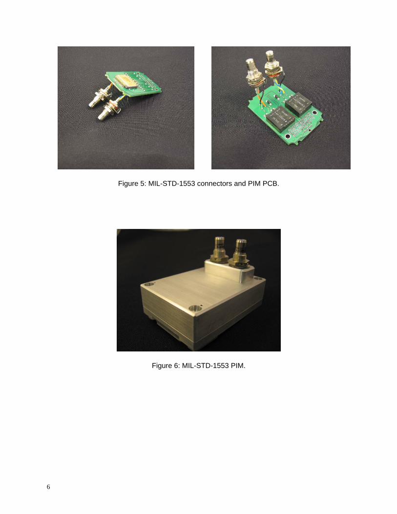
Figure 5: MIL-STD-1553 connectors and PIM PCB.
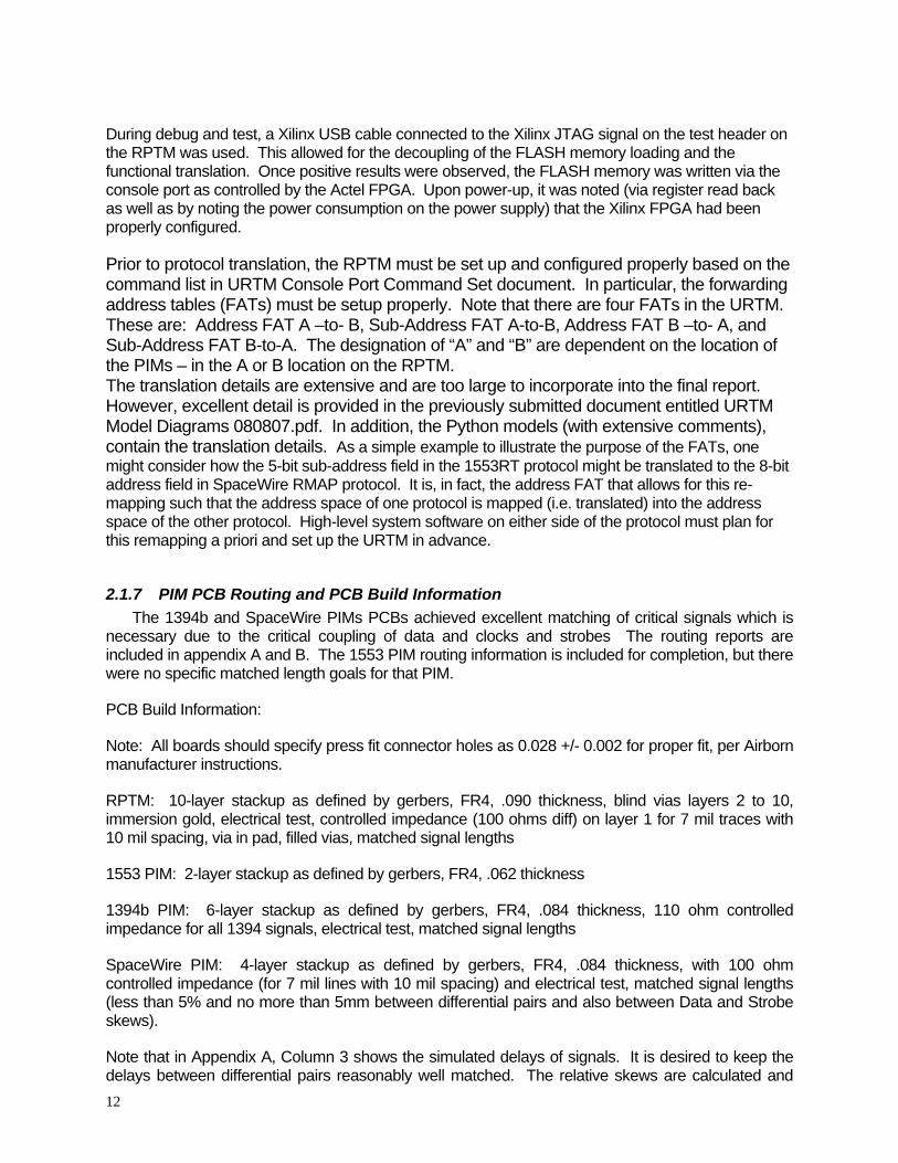
Figure 6: MIL-STD-1553 PIM.

7
Figure 7: SpaceWire connectors and PIM PCB (left) and PIM package (right).
Figure 8: URTM system with SpaceWire PIM (left) and 1553 PIM (right) attached to the RPTM.

8
2.1.1 Mass, Power and Volume Achievements An excellent compromise of all desired engineering goals have been met with a robust, functional
solution. The final specifications are shown in Table 1.
Table 1: Mass, power, and volume specs for each URTM module.
Module Mass (grams) Mass (oz) Power (Watts)
RPTM 220 7.8 5.61
1553b PIM 75 2.6 0.132
SpaceWire PIM 65 2.4 0.337
1394 PIM 80 3.0 0.825
Total Volume for the URTM with SpaceWire and 1553 PIMS (excluding projections for connectors) is approximately 76mm x 37mm x 87.5mm or 3” x 1.40” x 3.44”
Power consumption for a flight application could likely be significantly reduced for the RPTM. Only the VHDL for the two protocols involved in the translation would be loaded into the Xilinx translator FPGA at run-time. In order to simplify debug of successive loads across all protocols, and since the FPGA is large enough, Sigma selected to synthesize a “superset” of VHDL for all protocols into the Xilinx FPGA and used the PIM selection bits to multiplex the appropriate circuitry internally. Note also, the Xilinx ChipScope Pro option that assisted in debug efforts utilizes internal resources, primarily memory, which has a significant impact on power consumption. Note that the additional power required for debug activities is not reflected in the in Table 1. Smaller, FIFO buffers for the various protocols and sized for a specific application or mission, can also be used to save power, provided that the system-level use of the URTM allows for such savings.
2.1.2 Design Considerations with Regard to Space Flight The following design considerations were implemented in order to make the URTM design readily migratable to a space flight application: • Hooks for scrubbing (Actel / Xilinx) via Slave SelectMap Interface
• Use of flight-like or flight-equivalent components
• Room in Xilinx for TMR and other SEE mitigation approaches
• Triplicated I/O on Xilinx except for bi-directional signals
• Conductively cooled mechanical design
• Double-step corners for EMI
• Outgassing holes
• Flying leads on external connectors for mechanical decoupling
• Robust interconnect with ample compliance in the “Z” direction for high vibration environments

9
2.1.3 Flight Components Flight part equivalent components are available for all selected parts in existing footprints. The
engineering model has been populated with a variety of flight parts and commercial parts, where a commercial part could be used in the flight footprint. One example is that 0402 sized resistors were populated on pads designed to accept an 0502 sized flight resistor component. In other cases, such as with the oscillators, a dual footprint PCB design was employed that allows for the assembly with either the flight or commercial footprint on the same PCB.
The stacked FLASH memory from 3D-Plus used in the URTM design is planned to be migrated to a TMRed version. Initial versions shall utilize an FPGA and should be available by Q4 FY09 according to the manufacturer. A flight version with an ASIC within the 3-D stack will follow shortly thereafter. The path to flight for this component was independently verified with both Space Micro as well as with 3D-Plus. The TMR’ed part is a collaboration between the two vendors.
2.1.4 Key IP Cores and Components The RPTM Xilinx On-chip IP Cores include the following:
•1553 RT: Sital RT1553FE (Designed For 50 MHz operation)
•1553 BC: Sital BC1553FE (Designed For 50 MHz operation)
•SpaceWire: NASA Goddard Space Flight Center (GSFC) Space Wire Core (CD Date: 09/12/2007) Note: The SpaceWire buffer depth has been increased to 256 bytes from the original 64 bytes of the GSFC SpaceWire core. This was to better match the buffer sizes of the other interfaces while still maintaining the internal core timing and flow.
•1394b: DAP Technologies FireLink Basic
2.1.5 Key RPTM Devices & Interfaces: The key devices used on the RPTM card include the following: •Oscillator: 125 MHz Dual Footprint
•Configuration Device: Actel A54SX32A-CQ84 (RT54SX32S-84CQFP) via Xilinx Slave SelectMap Interface
•Console Port: Based On RS-232 Protocol, 8N1, Baud = 115200 bps Xilinx receives commands and transmits status via Actel FPGA to UART interface
•Test Header: FTE-110-02-G-DV-P for Xilinx JTAG, mode pins, and assorted test points
•Test Header: FTE-110-02-G-DV-P for Actel JTAG and probe signals
2.1.6 Key PIM On-Card Devices & Interfaces: The key devices used on the various PIMs include the following: •1553Transceiver: Aeroflex UT63M143-CCX (with Q1553-70 transformers)

10
•SpaceWire: Aeroflex UT54LVDM055LV-UPX LVDS Drivers / Receivers •1394b: TI TSB81BA3IPFPEP (or TSB81BA3D) 1394B 3-Port Cable
Transceiver/Arbiter with Pulse T-1062SCT (or T-1250SCT or T-1485SCT) transformers
The RPTM card contains two FPGAs, which control all functions of the URTM. One FPGA is an Actel A54SX32A-CQ84. This part has a space-flight path to the rad tolerant RT54SX32SU family. Therefore, this device is responsible for all FLASH memory, configuration, console communications functions. For a space-flight application, it can be used to scrub the Xilinx FPGA memory during operation. The other FPGA is a Xilinx XC4VLX200-10FF1513. This part has a path to flight, as it has a footprint compatible column grid array (CGA) device in the radiation hardened Virtex-4 QPro-V family. This device performs all translation functions for the URTM. A more detailed list of high-level FPGA functions is shown below:
Actel FPGA
The main functions of the Actel FPGA are as follows:
•Provides a console (UART) interface for user command and status (from both the Actel & Xilinx FPGAs)
•Provides a command/status interface to the Xilinx in order to forward received commands and to accept status from the Xilinx FPGA
•Provides a slave SelectMap interface to the Xilinx FPGA in order to perform configuration (and in the future, readback and scrubbing, if desired).
•Provides a controller for the Flash memory stack that can identify bad blocks, perform page reads and writes, perform block erases, and interface with the SelectMap controller block.
Xilinx FPGA
The Xilinx FPGA provides all buffering functions, reader, interpreter, writer, FAT, and RAT functionality for the translation process. It interfaces to the Actel FPGA for command & status (in addition to configuration) as well as to each PIM.

11
Functional Flow Block Diagram
CoreA
PIMA
Back-EndControl
&Tx / Rx FIFOs
(Note: SpW FIFOsare in Core)
Reader&
InterpreterPacketFIFO(Data)
FATs
RAT
Writer
CoreB
PIMB
Back-EndControl
&Tx / Rx FIFOs
(Note: SpW FIFOsare in Core)
Reader&
InterpreterPacketFIFO(Data)
FATs
RAT
Writer
Header & Controls
Header & Controls
(Read Only)
(Read Only)
Figure 9: URTM Functional Block Diagram
The internal architecture of the Xilinx FPGA follows the Python model created for this project. As such, each protocol has a reader/interpreter module as well as a writer module. Between these modules, there is a common set of forwarding address tables (FATs) for the address and sub-address fields, return address tables (RATs) for response packet mapping, and packet FIFOs for the buffering of full packets prior to writing during the translation process. In addition, since the user can select any two of the three PIMs for use and because the PIM locations (either A or B) on the RPTM are interchangeable, there is also a level of decoding a multiplexing not shown in the diagram, which allows for this flexibility. With the extra multiplexing, internal timing is not optimal. However, for the purposes of showing interoperability among the different protocols and without constraints on the A/B PIM designation, using a “superset” FPGA load was an excellent choice.
Note that when translating from a protocol of a “smaller” data width to a protocol of a “larger” data width the URTM implements a zero-padding scheme of the translated data. For example, when translating from 1553 to 1394b, 16-bit 1553 data is translated to 32-bit 1394b data fields. If there are an odd number of 1553 data words, then zero-padding is required in order to generate a complete 1394b message.
Note also that at this time, unrecognized transactions are transmitted out of the URTM input FIFOs so as to prevent the URTM from hanging or stalling on bad data. In the future, more complex handling and flagging can be implemented. In many cases, an error bit is set in the RPTM’s Error Register. If read, this register can alert the software that a 1394b, SpaceWire, 1553BC, or 1553RT error has occurred in the given protocol’s reader or writer interface.
12
During debug and test, a Xilinx USB cable connected to the Xilinx JTAG signal on the test header on the RPTM was used. This allowed for the decoupling of the FLASH memory loading and the functional translation. Once positive results were observed, the FLASH memory was written via the console port as controlled by the Actel FPGA. Upon power-up, it was noted (via register read back as well as by noting the power consumption on the power supply) that the Xilinx FPGA had been properly configured.
Prior to protocol translation, the RPTM must be set up and configured properly based on the command list in URTM Console Port Command Set document. In particular, the forwarding address tables (FATs) must be setup properly. Note that there are four FATs in the URTM. These are: Address FAT A –to- B, Sub-Address FAT A-to-B, Address FAT B –to- A, and Sub-Address FAT B-to-A. The designation of “A” and “B” are dependent on the location of the PIMs – in the A or B location on the RPTM. The translation details are extensive and are too large to incorporate into the final report. However, excellent detail is provided in the previously submitted document entitled URTM Model Diagrams 080807.pdf. In addition, the Python models (with extensive comments), contain the translation details. As a simple example to illustrate the purpose of the FATs, one might consider how the 5-bit sub-address field in the 1553RT protocol might be translated to the 8-bit address field in SpaceWire RMAP protocol. It is, in fact, the address FAT that allows for this re-mapping such that the address space of one protocol is mapped (i.e. translated) into the address space of the other protocol. High-level system software on either side of the protocol must plan for this remapping a priori and set up the URTM in advance.
2.1.7 PIM PCB Routing and PCB Build Information The 1394b and SpaceWire PIMs PCBs achieved excellent matching of critical signals which is
necessary due to the critical coupling of data and clocks and strobes The routing reports are included in appendix A and B. The 1553 PIM routing information is included for completion, but there were no specific matched length goals for that PIM.
PCB Build Information:
Note: All boards should specify press fit connector holes as 0.028 +/- 0.002 for proper fit, per Airborn manufacturer instructions.
RPTM: 10-layer stackup as defined by gerbers, FR4, .090 thickness, blind vias layers 2 to 10, immersion gold, electrical test, controlled impedance (100 ohms diff) on layer 1 for 7 mil traces with 10 mil spacing, via in pad, filled vias, matched signal lengths
1553 PIM: 2-layer stackup as defined by gerbers, FR4, .062 thickness
1394b PIM: 6-layer stackup as defined by gerbers, FR4, .084 thickness, 110 ohm controlled impedance for all 1394 signals, electrical test, matched signal lengths
SpaceWire PIM: 4-layer stackup as defined by gerbers, FR4, .084 thickness, with 100 ohm controlled impedance (for 7 mil lines with 10 mil spacing) and electrical test, matched signal lengths (less than 5% and no more than 5mm between differential pairs and also between Data and Strobe skews).
Note that in Appendix A, Column 3 shows the simulated delays of signals. It is desired to keep the delays between differential pairs reasonably well matched. The relative skews are calculated and

13
presented. The color codes help to reference the appropriate signals from the top of the list of signals. The highlighting serves to separate groups of signals. In Appendix A, colors on one page of that section correspond to the colors on the second page of that same section. This helps associate the PIM signals with the mismatch calculations. In Appendix B, the signal lengths are identical to the precision of the PCB tools, so no additional analysis is necessary. The signals are effectively “perfectly matched.”
2.1.8 Software Revisions Used to Generate Design Files The Actel software used for the URTM design is Libero version 8.3.
The Xilinx software used is ISE 10.1.02.
All license files and USB keys have been delivered to NASA.
2.1.9 Mechanical Features The original and augmented conductive cooling designs are shown in Figure 10. The augmented
design on the left includes conductive cooling for all regulators. Note that the extra aluminum for the regulators should be incorporated in the RPTM bottom panel if a new URTM case were to be machined. Note also that the heights of these are critical, and should be custom machined to match a particular RPTM PCB due to variations in lead-forming and soldering of the components to the PCB. ChoTherm was used as an interstitial material.
Outgassing holes for RPTM and each PIM have been implemented and engineered to outgas away from the mounting points. The mechanical design also incorporates an EMI enclosure with double-corner design, a robust interconnect between the RPTM and PIMs with ample compliance in the Z-direction (which is good for high vibration environments), and mechanically decoupled flying-lead connectors. These features are shown in Figure 10, Figure 11, Figure 12, Figure 13, and Figure 14.
Figure 10: Conductive cooling and mounting plate underneath the URTM package.

14
Figure 11: URTM package
Figure 12: EMI enhanced enclosure with double corner design.

15
Figure 13: Robust interconnect with ample compliance in the “Z” direction for high vibration environments.
Figure 14: External Connectors are mechanically decoupled via “Flying Lead” connections for all PIM I/O as well as for the console port connector.
16
2.2 URTM Performance The URTM successfully translates packets from the 1553, 1394b, and SpaceWire protocols. All of the goals regarding the protocol's bus rates have been achieved. They are as follows: 1553B: 1Mbit/sec
This was met and verified using our 1553 test equipment.
SpaceWire: 200 Mbit/sec (goal), 125 Mbit/sec (requirement)
As stated in the contract, the goal of the SpaceWire bit rate was 200 Mbits/sec with a minimum of 125 Mbits/sec. The outbound (URTM to SpaceWire) bit rate was set to 200 Mbit/sec and verified with the SpaceWire link analyzer. However, for the inbound traffic (SpaceWire Brick to URTM), the goal of 200 Mbits/sec was not met. In the SpaceWire Brick test software, options to run at 120 Mbits/sec or 140 Mbits/sec are available. The translation was not able to run at 140 Mbits/sec, but it was able to run at 120 Mbit/sec. Therefore, it was confirmed that this inbound bit rate was between 120 Mbits/sec and 140 Mbits/sec. Note, though, that the SpaceWire Brick test software does not allow the specification of 125 Mbits/sec. The 200Mbit/sec was demonstrated in that the SpaceWire Analyser has the capability to record the rates at which data is transferred. While transmitting nulls and data packets (i.e. while the link is open), the rates are shown on the bottom of the SpaceWire Analyser’s graphical user interface (GUI) where there is a portion of the window indicating “A->B” and “B->A” rates. In the current FPGA which provides for all three protocols in a multiplexed, superset fashion, the timing of the SpaceWire interface has not been optimized so it is likely that improvements can be made to the inbound side of the SpaceWire interface such that the 200 Mbit/sec rate (i.e. the goal) is achievable. 1394b: 800 Mbits/sec (goal), 400 Mbit/sec (requirement)
The 800 Mbits/sec rate was achieved with both a commercial 1394b connector initially populated on the 1394b PIM and later, with a military style 38999-type connector. The commercial connector was then removed from the PIM. Currently, streaming / isochronous packets between 1394b and SpaceWire are not supported. While the VHDL to perform such translation has been written, no testing or debugging of this packet translation has been performed. It should be noted that the URTM modeling allows for isochronous 1394b streams to be translated to SpaceWire RMAP data packets. Strictly speaking, SpaceWire does not allow for streaming packets, since it is not part of a recognized standard. However, the URTM models make a provision for this to be accomplished by exploiting the Protocol ID standard for the benefit of mapping this type of packet to/from 1394b streams packets.

17
2.2.1 Throughput There is no stated goal for throughput in the statement of work for this contract but rather a minimum and goal for each protocol’s bit rate. A throughput analysis was added per the COTR’s request to see the URTM is a potential bottleneck for the three protocols selected in this work. All contractual goals for protocol translation would still be met even if the URTM was a bottleneck. However, the translation would simply need to pause the faster of the two data paths and send shorter bursts of data rather than longer back-to-back packets of data. Each protocol was tested with its own unique piece of test equipment, each with its own constraints in terms of number of “back to back” and “at-speed” repetitive burst capabilities. No custom unifying software was developed in this contract that could compare data that was sent by one protocol tester to data that passed through the URTM and was received by another protocol tester. Such software would be essential to perform a hardware-based throughput analysis.
A throughput analysis has been conducted on the SpaceWire interface, since it provides the smallest token, hence smallest pipe, and the slowest throughput. For 1553 and 1394, the same process has a data path that is two times (1553) or four times (1394) wider, making the SpaceWire translation the potential bottleneck.
Reader Interpreter WriterRxQueue
TxQueue
PacketQueue
Dataflow Queuing Model Throughput Analys is of RPTM 2008-Sep-29 RJ, Sigma Space Corp
Critical Circuit: Time per token = 4 clock cycles per token (token=byte)
As s umptions : Que ue s provide a s ynchronous is ola tion be twe e n Re a de r, Inte rpre te r, a nd Da ta Links ;Me a s ure throughput of toke ns a t a ny conve nie nt a rc s hown a bove ; Toke n is the s ma lle s t indivis ible unit, which is the byte whe n proce s s ing SpW pa cke ts ; Critic al c irc uit de te rmine s wors t-ca s e e s tima teof throughput ca pa city for the RPTM in is ola tion, which is the 4-s ta te s e que nce of Inte rpre te r, a s this loop mus t comple te the full s e que nce for e a ch toke n – he nce the re d control toke n in the loop:
The re fore , wors t-ca s e throughput e s timate = 125E6 cycle s /s x 8 bits /toke n x 1 toke n/4 cycle s = 250 Mbps
Conc lus ion: RPTM is not the bottle ne ck; ra the r throughput is limite d by the s lowe s t da ta link protocol

18
In conclusion, a model of the RPTM throughput shows that the minimum throughput capacity is about 250 Mbps and that the RPTM is not the bottleneck; the bottleneck is the slowest data link.
2.2.2 Translation Performance The transactions shown in Table 2 have been exercised. Some combinations could not be exercised due to our test setup during this research project. For example, testing the SpaceWire or 1394b to 1553 when the PIM was a 1553RT did not occur. In such a case, the URTM can only respond to a 1553BC out on the bus. For this to occur, the test setup would need to be a closed loop system wherein the BC could send a command to the SpaceWire or 1394b device via the URTM. The SpaceWire or 1394b device would then respond in a timely manner via the URTM. In the future, more at-speed, rigorous testing should be performed.
Table 2: URTM Transactions Exercised
Tester Core Core TesterRT, Sends Write Response 1553BC SpW Receives Write ResponseRT, Sends Read Response 1553BC SpW Receives Read ResponseRT, Sends Write Response 1553BC 1394b Receives Write ResponseRT, Sends Read Response 1553BC 1394b Receives Read ResponseBC, Sends Write Command 1553RT SpW Receives Write CommandBC, Sends Write Command 1553RT 1394b Receives Write CommandSpW Sends Write Command SpW 1553BC RT, Receives Write CommandSpW Sends Read Command SpW 1553BC RT, Receives Read CommandSpW Sends Write Command SpW 1394b 1394b Receives Write Quadlet CommandSpW Sends Write Command SpW 1394b 1394b Receives Write Block CommandSpW Sends Read Command SpW 1394b 1394b Receives Read Block CommandSpW Sends Read Response SpW 1553RT BC, Receives Read ResponseSpW Sends Write Response SpW 1553RT BC, Receives Write ResponseSpW Sends Read Response SpW 1394b 1394b Receives Read Block ResponseSpW Sends Write Response SpW 1394b 1394b Receives Write ResponseSpW Sends RMW Response SpW 1394b 1394b Receives RMW Response1394b Sends Write Quadlet Command 1394b 1553BC RT, Receives Write Quadlet Command1394b Sends Write Block Command 1394b 1553BC RT, Receives Write Block Command1394b Sends Read Block Command 1394b 1553BC RT, Receives Read Block Command1394b Sends Write Quadlet Command 1394b SpW SpW Receives Write Quadlet Command1394b Sends Write Block Command 1394b SpW SpW Receives Write Block Command1394b Sends Read Block Command 1394b SpW SpW Receives Read Block Command1394b Sends Lock (RMW) Command 1394b SpW SpW Receives Lock (RMW) Command1394b Sends Write Response 1394b SpW SpW Receives Write Response1394b Sends Read Quadlet Response 1394b SpW SpW Receives Read Response
2.2.3 Test Software At this time, all URTM testing has been performed with the test equipment purchased under the
project, coupled with a custom console interface software program that provides URTM specific needs such as access to the FLASH memory, tracking and management of bad memory blocks, and convenient access to URTM registers. No custom, high level software was written to perform closed-loop, testing. Rather, packet transmission via one protocol tester has been exercised with the resulting packet reception observed by the other protocol tester. In all cases, the packet transmission / reception tests have been run in a single, one-at-a-time mode. Additionally, where possible, back-to-back, "high rate" (limited only by the tester itself) transmission & reception testing has been performed. For example, in the case of the 1553 tester, when tester is acting as a 1553 bus controller (BC) and the URTM has the 1553 PIM acting as a remote terminal (RT), continuous packets to the SpaceWire or 1394b interfaces can be sent. Since 1553 is the slowest interface, running at 1 Mbit/sec, there are no concerns as continuous packets are sent to the 800 Mbit/sec 1394b interface or the 200 Mbit/sec SpaceWire interface. Likewise, when testing the 1394b

19
interface, any number from 1 to 999 packets can be sent to the 1553 or SpaceWire interfaces. However, in this case, 1394b is the fastest interface. It is not a fair test to send nearly continuous, or long burst data to the 1 Mbit/sec 1553 interface; sending to the SpaceWire interface is also questionable since it the bus rate is 1/4 of the 1394b rate. In the case of the SpaceWire tester, since the RMAP protocol is being used, a method in which to send continuous or large burst RMAP packets was not determined. Using the SpaceWire tester's CUBA software, a "batch" file of commands was generated and set, but this generated via a copy-and-paste approach, and therefore, cannot be without bounds. In this case, six back-to-back RMAP packets were sent as fast as possible via the tester, and they were successfully translated to the 139b protocol.
The transmitted packets were manually compared by visually checking that the transmitted command and data were correctly translated and received. When the counter was updated by the receiving test equipment, one could confirm that a valid packet was received. This means that all headers, data fields of proper length (as per the header information), and valid checksums (such as CRCs) were all generated by the URTM and sent to this receiving test equipment. That is, the headers, data payload, and error correction fields were all valid for the given packet. Since there was no closed-loop software to analyze all transmitted data and compare this data to received data for large data sets, the transmit counters and receive counters provided by the test equipment allowed for the validation that the total number of expected packets were sent and received properly.
2.2.4 FPGA Utilization and Timing Performance The FPGA utilization for the Xilinx XC4VLX200-10FF1513, bitstream version load number 0x59 (identified by the Scratchpad Register default value) is shown it Table 3 below.

20
Device Utilization Summary [-] Logic Utilization Used Available Utilization Note(s) Number of Slice Flip Flops 6,031 178,176 3% DCM autocalibration logic 42 6,031 1% Number of 4 input LUTs 10,365 178,176 5% DCM autocalibration logic 24 10,365 1% Logic Distribution Number of occupied Slices 9,065 89,088 10% Number of Slices containing only related logic 9,065 9,065 100% Number of Slices containing unrelated logic 0 9,065 0% Total Number of 4 input LUTs 10,996 178,176 6% Number used as logic 9,568 Number used as a route-thru 631 Number used as 16x1 RAMs 56 Number used for Dual Port RAMs 640 Number used as Shift registers 101 Number of bonded IOBs
Number of bonded 282 960 29% IOB Flip Flops 15 Number of BUFG/BUFGCTRLs 13 32 40% Number used as BUFGs 12 Number used as BUFGCTRLs 1 Number of FIFO16/RAMB16s 76 336 22% Number used as RAMB16s 76 Number of DCM_ADVs 6 12 50%
Table 3: Xilinx FPGA Utilization
The Xilinx FPGA routed completely. Three timing violations were flagged as failed. Two of the three violations had to do with the asynchronous clock-crossing boundary within the SpaceWire core where the 200 MHz data-strobe clock and the back-end's 125 MHz clock interact. Per the core's literature, the use of multiple clocks is allowed, since the core should handle the interfacing properly. Likely, the constraint should be marked as a false path, but at this time, this has not been investigated further. The third issue was a clock skew issue on the 200 MHz rising/falling edges. As above, this has not been researched further, but by marking false paths properly, and by optimizing the constraints, the failed path can likely be removed.

21
The utilization of the Actel A54SX32S FPGA is shown in Table 4.
SEQUENTIAL Used: 742 Total: 1080 (68.70%) COMB Used: 1432 Total: 1800 (79.56%) LOGIC Used: 2174 Total: 2880 (75.49%) (seq+comb) IO w/ Clocks Used: 52 Total: 59 CLOCK Used: 2 Total: 2 HCLOCK Used: 1 Total: 1
Table 4: Actel FPGA Utilization
The Actel FPGA routed completely and met all timing requirements. In a flight application, there would likely be additional logic added to perform the function of a scrubber for the Xilinx FPGA. Note that depending on the encoding of the various state machines within the Actel FPGA, significant utilization resources were observed. For example, the utilization ranged from approximately 68% to 79% depending if a one-hot encoding or gray encoding was selected. At this time, such encoding has not been optimized but could be optimized in the future.
22
3 Lessons Learned
3.1 Models Independent validation of functionality via higher-level modeling has again proven useful and has
also reduced the number of functional, logical, and control errors that would otherwise have dominated the debug effort.
3.2 ChipScope Pro The ChipScope Pro tool is extremely useful for large, multi-core, system-on-a-chip type designs.
It functions as a virtual logic analyzer with triggering capability, to see busses, control signals, and user selected nets. The use of the tool saved many weeks of integration time on the URTM project.

23
4 Future Work
4.1 Robustness Improvements The URTM was tested in a manual mode, not a closed-loop, rigorously tested setting. Before
being used in a "real" application, such testing is essential. This kind of testing should be comprised of both small and large packets that are transferred via the URTM in a back-to-back, "at-speed" manner and with different types of packet formats intermingled.
Other improvements that would provide robustness would be to make the URTM more resistant to problems and exceptional behavior. One way to accomplish this would be to employ automatic flushing of FIFOs when illegal packets are received by the URTM along with more error reporting.
4.2 Multi-split Transaction Handling The address forwarding/return table was implemented in its more basic form. As is, the URTM
supports only one virtual circuit between source and sink at a time, though in both directions (full duplex). Multiple virtual circuits in a given direction is not supported at this time because the “transaction label” is not stored and properly managed with the addressing within the forward/return tables. The design is well understood and documented in the presentation packages, just not implemented in favor of working on more challenging problems. Future work in this area can easily support multiple split transactions.
4.3 SpaceWire Protocol
4.3.1 Path Addressing for SpaceWire SpaceWire packets can be routed by either logical addressing or path addressing. The preferred
approach is path addressing because it puts the complexity of routing with the routers, as opposed to all of the network nodes (end points). This was our preferred approach as well for this URTM prototype. Supporting path addressing is straightforward, only requiring a more complex management of the forward/return address tables.
4.3.2 Time Codes for SpaceWire The SpaceWire protocol has special packets called “time codes” that support a distributed time
synchronization algorithm. This is most important for distributed computer systems at the end points. There is little benefit of having a URTM bridge process time codes, as it does not currently keep time. However, applications in the future may have a need to have time synchronization between the two networked bridged by a URTM. This would require that the URTM process time codes and synchronize its time with the SpaceWire network so that it could, in turn, synchronize nodes on the bridged network.
4.4 IEEE 1394 Protocol
4.4.1 Asynchronous Stream Packets The URTM currently implements asynchronous transaction packets and is set up to support
isochronous stream packets. This allows the best, seamless translation between the (three) targeted protocols. There is a third 1394 packet type called the asynchronous stream packet. It is essentially a combination of the former two packets: asynchronous stream packets are isochronous packets that

24
are transmitted in the asynchronous arbitration period. Asynchronous stream packets can be incorporated straightforwardly in future developments.
4.4.2 SAE AS56453 Protocol The AS5643 protocol, sometimes referred to as “Mil-Std-FireWire,” uses full use of asynchronous
stream packets, primarily, and only the other two packet types secondarily. So, once asynchronous stream packets are implemented, AS5643 protocol can be incorporated. Doing so would also require some lightweight, higher-level protocol on top of the data link layer where the URTM currently operates. The AS5643 protocol is normally implemented in software above the data link layer, which is hardware. AS5643 can most likely be accommodated in software, too, by making use of the MicroBlaze embedded microprocessor. MicroBlaze even supports C software development on a Linux OS. Of course, space applications requiring SEE mitigation would require that the MicroBlaze be replicated in a voting scheme. This is likely possible within the current FPGA resource availability and margins.
4.5 Time-Triggered Ethernet Protocol The time-triggered Ethernet protocol, or TTE, could support interesting and useful applications in
embedded industrial, automotive, and aerospace systems. Sigma Space has studied the feasibility of integrating the TTE in the existing URTM concept, architecture, and design. The technical aspects considered were limited in scope and detail to be high level, conceptual, logical, temporal, and physical. Salient features of the TTE specification and the prior art of implementation were considered that most impact the URTM design. Our conclusion is that integrating the TTE protocol would be straightforward. Indeed, it is anticipated that the task would be easier than the work required to accommodate IEEE 1394, and much cheaper, too. TTE technology already enjoys inexpensive, commercially available hardware and software suitable for prototyping, hosting, and testing. Backwards compatibility with standard Ethernet hardware and software tools would also facilitate and reduce the cost of test equipment, drivers, IP cores, programming and debugging environments, and demonstration systems. TTE would, therefore, make a nice addition to the URTM protocol suite. A full report on this protocol has been delivered to NASA LaRC under separate cover.

25
5 Appendix A: 1394 PIM Routing Report Pim 1394Ruoted report
NET Ruoted Length (mils) dealy(ns) Net Class Port#TPA2_N 653.69 0.093 TP_BUS 2TPA2_P 584.75 0.083 TP_BUS 2TPB2_N 886.95 0.126 TP_BUS 2TPB2_P 882 0.125 TP_BUS 2TPA1_N 750.63 0.107 TP_BUS 11394_RX1_N 314.96 0.045 1394_CON 1TPA1_P 775 0.110 TP_BUS 11394_RX1_P 286.94 0.041 1394_CON 1TPB1_N 495.06 0.070 TP_BUS 11394_TX1_N 647.78 0.092 1394_CON 1TPB1_P 523.91 0.074 TP_BUS 11394_TX1_P 619.72 0.088 1394_CON 1TPA0_N 808.44 0.115 TP_BUS 01394_RX0_N 329.98 0.047 1394_CON 0TPA0_P 837.79 0.119 TP_BUS 01394_RX0_P 302.64 0.043 1394_CON 0TPB0_N 487.13 0.069 TP_BUS 01394_TX0_N 683.12 0.097 1394_CON 0TPB0_P 516.89 0.073 TP_BUS 01394_TX0_P 654.95 0.093 1394_CON 0TPBIAS0 475.83 0.068 TP_BIASTPBIAS1 467.89 0.066 TP_BIASTPBIAS2 289.93 0.041 TP_BIASTPA2_RTN 322.99 0.046 TP_BIASTPB0_T 176.21 0.025 TP_BIASTPB1_T 245.36 0.035 TP_BIASTPB2_T 192.06 0.027 TP_BIAS+3_3V 2301.39 0.327 POWER+1_95VP 411.96 0.058 POWER+3_3VA 581.75 0.083 POWER+1_95V 2221.55 0.315 POWER+3_3VP 251.89 0.036 POWERVCC_OSC 597.26 0.085 POWERBUS_PWR 184.81 0.026 POWERPIM_KEY0 248.28 0.035 PIM_KEYPIM_KEY1 128.62 0.018 PIM_KEYPIM_KEY2 175.05 0.025 PIM_KEYPIM_KEY3 235.42 0.033 PIM_KEYDGND 1936.28 0.275 GNDSHELL 170.95 0.024 GNDCGND 866.74 0.123 GNDPHY_DATA2 288.26 0.041 DATA_BUS_FPGAPHY_DATA7 390.96 0.055 DATA_BUS_FPGAPHY_DATA1 353.01 0.050 DATA_BUS_FPGAPHY_DATA0 270.36 0.038 DATA_BUS_FPGAPHY_DATA3 299.85 0.043 DATA_BUS_FPGAPHY_DATA4 382.25 0.054 DATA_BUS_FPGAPHY_DATA5 428.93 0.061 DATA_BUS_FPGAPHY_DATA6 360.13 0.051 DATA_BUS_FPGAPHY_RESET 528.07 0.075 CTRL_FPGAPHY_PCLK 220.11 0.031 CTRL_FPGAPHY_LPS 521.81 0.074 CTRL_FPGAPHY_LINKON 113.81 0.016 CTRL_FPGAPCLK 95.02 0.013 CTRL_FPGALKON 151.93 0.022 CTRL_FPGALCLK 204.75 0.029 CTRL_FPGA1394_BMODE 345.99 0.049 CTRL_FPGAPHY_CTL0 255.6 0.036 CTRL_FPGAPHY_CTL1 337.98 0.048 CTRL_FPGAPHY_LCLK 125.71 0.018 CTRL_FPGAPHY_LREQ 333.11 0.047 CTRL_FPGAPHY_PINT 400.6 0.057 CTRL_FPGACLK_98MHZ_18 127.45 0.018 CLK_98MHZOSC_98MHZ 297.98 0.042 CLK_98MHZPC2 461.53 0.065 1394_CONFIGPC1 457.52 0.065 1394_CONFIGPC0 457.99 0.065 1394_CONFIGDS1 412.53 0.059 1394_CONFIGDS0 493.09 0.070 1394_CONFIGR0 176.12 0.025 1394_CONFIG

26
Diff Pair Mistmatch(mils) Diff Pair Mistmatch(ns) RX to TX mismatch (mils) RX to TX mismatch (ns)68.94 0.010 63.99 0.009
4.95 0.001
3.65 0.001 4.44 0.001
-0.79 0.000
-2.01 0.000 -0.42 0.000
-1.59 0.000

27
6 Appendix B: SpaceWire PIM Routing Report Pim Space WireRuoted report
NET Ruoted Length (mils) Net Class Match Lengh GroupR_RXS- 514.41 100_OHM_DIFF MLNetGroup2R_RXD- 514.41 100_OHM_DIFF MLNetGroup2R_RXD+ 514.41 100_OHM_DIFF MLNetGroup2R_RXS+ 514.41 100_OHM_DIFF MLNetGroup2P_RXD+ 514.41 100_OHM_DIFF MLNetGroup2P_RXD- 514.41 100_OHM_DIFF MLNetGroup2P_RXS+ 514.41 100_OHM_DIFF MLNetGroup2P_RXS- 514.41 100_OHM_DIFF MLNetGroup2P_TXD+ 514.41 100_OHM_DIFF MLNetGroup2P_TXD- 514.41 100_OHM_DIFF MLNetGroup2P_TXS+ 514.41 100_OHM_DIFF MLNetGroup2P_TXS- 514.41 100_OHM_DIFF MLNetGroup2R_TXD+ 514.41 100_OHM_DIFF MLNetGroup2R_TXD- 514.41 100_OHM_DIFF MLNetGroup2R_TXS+ 514.41 100_OHM_DIFF MLNetGroup2R_TXS- 514.41 100_OHM_DIFF MLNetGroup2PSTROBE_TX 1383.91 DATA_FPGA MLNetGroup1PDATA_RX 1383.91 DATA_FPGA MLNetGroup1PDATA_TX 1383.91 DATA_FPGA MLNetGroup1PSTROBE_RX 1383.91 DATA_FPGA MLNetGroup1RDATA_RX 1383.91 DATA_FPGA MLNetGroup1RDATA_TX 1383.91 DATA_FPGA MLNetGroup1RSTROBE_RX 1383.91 DATA_FPGA MLNetGroup1RSTROBE_TX 1383.91 DATA_FPGA MLNetGroup1+3_3V 4475.18 POWERDGND 0PIM_KEY0 116.02PIM_KEY1 126.38PIM_KEY2 113.95PIM_KEY3 124.31PTXOE 1076 DATA_FPGARTXOE 1400.35 DATA_FPGA

28
7 Appendix C: 1553 PIM Routing Report PIM1553
Routted report No Matched Length signals required for 1553
NET Routed Length (mils) Net Class
Match Lengh Group
TXRX_B_N 1715.26 0 0TXRX_B 1509.24 0 0TXRX_A_N 1806.08 0 0TXRX_A 1743.44 0 0S_BUSB_P 347.12 0 0S_BUSB_N 232.86 0 0S_BUSA_P 235.86 0 0S_BUSA_N 344.26 0 0S8B 170.36 0 0S8A 167.36 0 0S7B 170.36 0 0S7A 172.77 0 0S5B 171.36 0 0S5A 169.01 0 0S4B 171.18 0 0S4A 167.36 0 0PIM_KEY3 147.09 0 0PIM_KEY2 136.73 0 0PIM_KEY1 126.38 0 0PIM_KEY0 116.02 0 0DGND 359.57 0 01553_TX_INH_B 964.54 0 01553_TX_INH_A 1163.39 0 01553_TX_B_N 1026.89 0 01553_TX_B 1163.58 0 01553_TX_A_N 1360.47 0 01553_TX_A 1184.95 0 01553_PLUS_B 2488.09 0 01553_PLUS_A 2139.28 0 01553_MINUS_B 2188.71 0 01553_MINUS_A 2017.45 0 01553_BUSB_P 193.21 0 01553_BUSB_N 347.28 0 01553_BUSA_P 193.21 0 01553_BUSA_N 342.83 0 0+3_3V 4267.23 0 0

29
8 Appendix D: PIM Pinout Table
ConnPosition Pin #
1553 PIMRC442-052-321-4100
SpW PIMRC442-052-321-4100
1394 PIMRC442-052-321-4100
RPTMRC422-052-101-3000
RPTMInput/Output
Outer 1 +3.3V +3.3V +3.3V +3.3V PowerOuter 2 SPW_RSTROBE_TX SPW_RSTROBE_TX OutputOuter 3 SPW_RTXOE SPW_RTXOE OutputOuter 4 NCGND SPW_RDATA_RX NCGND SPW_RDATA_RX InputOuter 5 SPW_RDATA_TX SPW_RDATA_TX OutputOuter 6 PIM_KEY3 PIM_KEY3 PIM_KEY3 PIM_KEY3 InputOuter 7 PIM_KEY2 PIM_KEY2 PIM_KEY2 PIM_KEY2 InputOuter 8 PIM_KEY1 PIM_KEY1 PIM_KEY1 PIM_KEY1 InputOuter 9 PIM_KEY0 PIM_KEY0 PIM_KEY0 PIM_KEY0 InputOuter 10 1553_MINUS_B NCGND NCGND 1553_MINUS_B InputOuter 11 1553_TX_A_N 1553_TX_A_N OutputOuter 12 1553_PLUS_A NCGND NCGND 1553_PLUS_A InputOuter 13 GND GND GND GND GNDInner 14 SPW_PTXOE SPW_PTXOE OutputInner 15 GND GND GND GND GNDInner 16 NCGND SPW_RSTROBE_RX NCGND SPW_RSTROBE_RX InputInner 17 GND GND GND GND GNDInner 18 GND GND GND GND GNDInner 19 1553_TX_B 1553_TX_B OutputInner 20 1553_TX_B_N 1553_TX_B_N OutputInner 21 1553_TX_INH_B 1553_TX_INH_B OutputInner 22 1553_PLUS_B NCGND NCGND 1553_PLUS_B InputInner 23 1553_TX_A 1553_TX_A OutputInner 24 1553_TX_INH_A 1553_TX_INH_A OutputInner 25 1553_MINUS_A NCGND NCGND 1553_MINUS_A InputInner 26 +1.95V +1.95V PowerInner 27 +3.3V +3.3V +3.3V +3.3V PowerInner 28 NCGND SPW_PDATA_RX NCGND SPW_PDATA_RX InputInner 29 NCGND SPW_PSTROBE_RX NCGND SPW_PSTROBE_RX InputInner 30 1394_PHY_LPS 1394_PHY_LPS OutputInner 31 NCGND NCGND 1394_PHY_PINT 1394_PHY_PINT InputInner 32 1394_PHY_LREQ 1394_PHY_LREQ OutputInner 33 NCGND NCGND 1394_PHY_PCLK 1394_PHY_PCLK InputInner 34 1394_PHY_CTL1 1394_PHY_CTL1 BiDirInner 35 1394_PHY_DATA1 1394_PHY_DATA1 BiDirInner 36 GND GND GND GND GNDInner 37 1394_PHY_DATA4 1394_PHY_DATA4 BiDirInner 38 1394_PHY_DATA5 1394_PHY_DATA5 BiDirInner 39 GND GND GND GND GNDOuter 40 GND GND GND GND GNDOuter 41 SPW_PDATA_TX SPW_PDATA_TX OutputOuter 42 SPW_PSTROBE_TX SPW_PSTROBE_TX OutputOuter 43 1394_PHY_RESET 1394_PHY_RESET OutputOuter 44 NCGND NCGND 1394_PHY_LINKON 1394_PHY_LINKON InputOuter 45 1394_PHY_LCLK 1394_PHY_LCLK OutputOuter 46 1394_PHY_CTL0 1394_PHY_CTL0 BiDirOuter 47 1394_PHY_DATA0 1394_PHY_DATA0 BiDirOuter 48 1394_PHY_DATA2 1394_PHY_DATA2 BiDirOuter 49 1394_PHY_DATA3 1394_PHY_DATA3 BiDirOuter 50 GND GND GND GND GNDOuter 51 1394_PHY_DATA6 1394_PHY_DATA6 BiDirOuter 52 NCGND NCGND 1394_PHY_DATA7 1394_PHY_DATA7 BiDir
URTM: RPTM / PIM Interface Connector Mapping: 52 Pins

REPORT DOCUMENTATION PAGE Form ApprovedOMB No. 0704-0188
2. REPORT TYPE Contractor Report
4. TITLE AND SUBTITLEUniversal Reconfigurable Translator Module (URTM) Final Report
5a. CONTRACT NUMBER
NNL07AA25C
6. AUTHOR(S)
Leventhal, Edward; Machan, Roman; Jones, Rob
7. PERFORMING ORGANIZATION NAME(S) AND ADDRESS(ES)NASA Langley Research Center Sigma Space CorporationHampton, VA 23681-2199 4801 Forbes Blvd. Lanham, MD 20706
9. SPONSORING/MONITORING AGENCY NAME(S) AND ADDRESS(ES)National Aeronautics and Space AdministrationWashington, DC 20546-0001
8. PERFORMING ORGANIZATION REPORT NUMBER
10. SPONSOR/MONITOR'S ACRONYM(S)
NASA
13. SUPPLEMENTARY NOTES
Langley Technical Monitor: Tak-Kwong Ng
12. DISTRIBUTION/AVAILABILITY STATEMENTUnclassified - UnlimitedSubject Category 33Availability: NASA CASI (443) 757-5802
19a. NAME OF RESPONSIBLE PERSON
STI Help Desk (email: [email protected])
14. ABSTRACT
This report describes the Universal Reconfigurable Translation Module, or URTM. The URTM was developed by Sigma Space Corporation for NASA in order to translate specific serial protocols, both logically and physically. At present, the prototype configuration has targeted MIL-STD-1553B (RT and BC), IEEE 1394b (Firewire), and ECSS-E-50-12A (SpaceWire). The objectives of this program were to study the feasibility of a configurable URTM to translate serial link data as might be used in a space-flight mission and to design, develop, document, and deliver an engineering prototype model of the URTM with a path to spaceflight. By simply connecting two of the three Physical Interface Modules (PIM) on either end of the RPTM (Reconfigurable Protocol Translator Module), the URTM then self configures via a library of interface translation functions, thereby allowing the two data links to communicate seamlessly.
15. SUBJECT TERMSUniversal ReconfigurableTranslator Module; URTM; SpaceWire; Filed Programmable Gate Arrays; FPGA
18. NUMBER OF PAGES
3419b. TELEPHONE NUMBER (Include area code)
(443) 757-5802
a. REPORT
U
c. THIS PAGE
U
b. ABSTRACT
U
17. LIMITATION OF ABSTRACT
UU
Prescribed by ANSI Std. Z39.18Standard Form 298 (Rev. 8-98)
3. DATES COVERED (From - To)27-03-2007 to 30-09-2008
5b. GRANT NUMBER
5c. PROGRAM ELEMENT NUMBER
5d. PROJECT NUMBER
5e. TASK NUMBER
5f. WORK UNIT NUMBER
198059.04.06.04
11. SPONSOR/MONITOR'S REPORT NUMBER(S)
NASA/CR-2009-215744
16. SECURITY CLASSIFICATION OF:
The public reporting burden for this collection of information is estimated to average 1 hour per response, including the time for reviewing instructions, searching existing data sources, gathering and maintaining the data needed, and completing and reviewing the collection of information. Send comments regarding this burden estimate or any other aspect of this collection of information, including suggestions for reducing this burden, to Department of Defense, Washington Headquarters Services, Directorate for Information Operations and Reports (0704-0188), 1215 Jefferson Davis Highway, Suite 1204, Arlington, VA 22202-4302. Respondents should be aware that notwithstanding any other provision of law, no person shall be subject to any penalty for failing to comply with a collection of information if it does not display a currently valid OMB control number.PLEASE DO NOT RETURN YOUR FORM TO THE ABOVE ADDRESS.
1. REPORT DATE (DD-MM-YYYY)05 - 200901-