Embed Size (px)
Citation preview

UNIT II
MIDBAND ANALYSIS OF SMALL SIGNAL AMPLIFIERS
CE, CB and CC amplifiers. Method of drawing small-signal equivalent circuit. Midband analysis of various types of single stage amplifiers to obtain gain, input impedance and output impedance. Miller’s theorem. Comparison of CB, CE and CC amplifiers and their uses. Darlington connection using similar and Complementary transistors. Methods of increasing input impedance using Darlington connection and bootstrapping. CS, CG and CD (FET) amplifiers. Multistage amplifiers. Basic emitter coupled differential amplifier circuit. Bisection theorem. Differential gain. CMRR. Use of constant current circuit to improve CMRR. Derivation of transfer characteristic, Transconductance. Use as Linear amplifier, limiter, amplitude modulator. Objectives:
• Identify and apply internal transistor parameters • Analyze the operation of common-emitter amplifiers • Analyze the operation of common-collector amplifiers • Analyze the operation of common-base amplifiers • Discuss multistage amplifiers and analyze their operation • Describe the amplification properties of a FET • Explain and analyze the operation of common-source FET amplifiers • Explain and analyze the operation of common-drain FET amplifiers
2.1 Methods of drawing small signal equivalent circuit
The key to the small-signal approach is the use of ac equivalent circuits or models. There are two methods regarding the equivalent circuit to be substituted for the transistor, the hybrid parameters and the re model .A model is the combination of circuit elements, properly chosen, that best approximates the actual behavior of BJT under specific operating conditions, In summary the ac equivalent circuit of BJT amplifier is obtained by:
1- Setting all dc sources to zero-potential equivalent and replacing them by a short circuit connection to ground.
2-replacing all capacitors short circuit equivalent. 3-Removing all element bypassed by the short circuit equivalents introduced by steps 1& 2 4-Redrawing the circuit in a more convenient and logical forms (Fig2-3).

Fig 2-1 Transistor circuit under examination Fig 2-2 the network of Fig2-1 the short circuit equivalent
Fig 2-3 small-signal ac analysis
5-use the hybrid or re equivalent circuit of the BJT to complete the equivalent circuit ofthe amplifier 6- Finally, the following important parameters are determined for the amplifier:
• Input impedance Zi • Output impedance Zo • Voltage gain Av • Current gain Ai
• phase relationship ( ) 2.1.1 The re Transistor Model
The re model employs a diode and controlled current source to duplicate the behavior of a transistor. A current-controlled current Sources is one where the parameters of the current source are controlled by a current else where in the network, in general BJT transistor amplifiers are referred to as current-controlled device.
2.1.2 The Hybrid equivalent model _ For the hybrid equivalent model, the parameters are defined at an operating point. _ The quantities hie, hre,hfe, and hoe are called hybrid parameters and are the components of a small – signal equivalent circuit. • The description of the hybrid equivalent model will begin with the general two port system.

Fig a
• The set of equations in which the four variables can be related are: • Vi = h11Ii + h12Vo • Io = h21Ii + h22Vo • The four variables h11, h12, h21 and h22 are called hybrid parameters ( the mixture of variables in each equation results in a “ hybrid” set of units of measurement for the h – parameters. • Set Vo = 0, solving for h11, h11 = Vi / Ii Ohms • This is the ratio of input voltage to the input current with the output terminals shorted. It is called Short circuit input impedance parameter. • If Ii is set equal to zero by opening the input leads, we get expression for h12: h12 = Vi / Vo , This is called open circuit reverse voltage ratio. • Again by setting Vo to zero by shorting the output terminals, we get h21 = Io / Ii known as short circuit forward transfer current ratio. • Again by setting I1 = 0 by opening the input leads, h22 = Io / Vo . This is known as open – circuit output admittance. This is represented as resistor ( 1/h22) • h11 = hi = input resistance • h12 = hr = reverse transfer voltage ratio • h21 = hf = forward transfer current ratio • h22 = ho = Output conductance 2.1.3 Hybrid Input and output equivalent circuit
Fig b Hybrid input equivalent circuit Fig c Hybrid output equivalent circuit 2.1.4 Complete hybrid equivalent circuit

Fig d 2.1.5 Common Emitter Configuration - hybrid equivalent circuit
Fig e Essentially, the transistor model is a three terminal two – port system. • The h – parameters, however, will change with each configuration. • To distinguish which parameter has been used or which is available, a second subscript has been added to the h – parameter notation. • For the common – base configuration, the lowercase letter b is added, and for common emitter and common collector configurations, the letters e and c are used respectively. 2.1.6 Common Base configuration - hybrid equivalent circuit
Fig f
Table 1

2.1.7 Approximate hybrid equivalent circuit Normally hr is a relatively small quantity, its removal is approximated by hr = 0 and hrVo = 0, resulting in a short – circuit equivalent. • The resistance determined by 1/ho is often large enough to be ignored in comparison to a parallel load, permitting its replacement by an open – circuit equivalent.
Fig g
h-Parameter Model v/s. re Model
hie = re, hfe = ac
Common Base: re v/s. h-Parameter Model
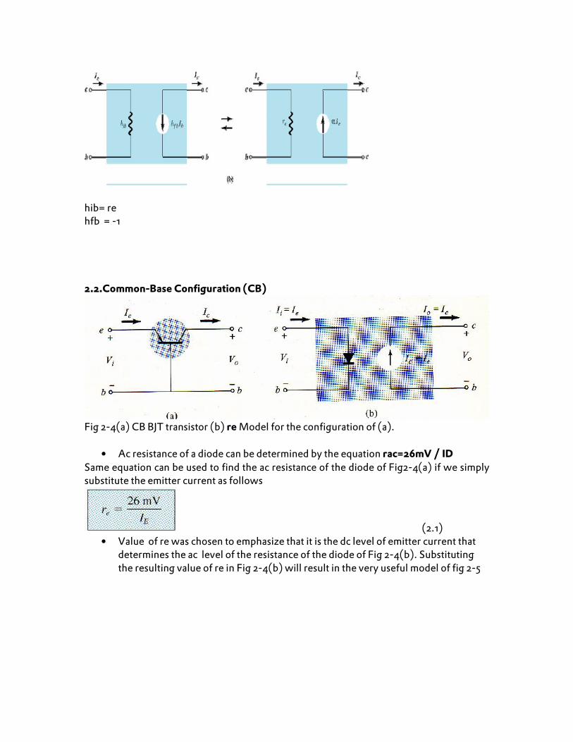
hib= re hfb = -1 2.2.Common-Base Configuration (CB)
Fig 2-4(a) CB BJT transistor (b) re Model for the configuration of (a).
• Ac resistance of a diode can be determined by the equation rac=26mV / ID Same equation can be used to find the ac resistance of the diode of Fig2-4(a) if we simply substitute the emitter current as follows
(2.1) • Value of re was chosen to emphasize that it is the dc level of emitter current that
determines the ac level of the resistance of the diode of Fig 2-4(b). Substituting the resulting value of re in Fig 2-4(b) will result in the very useful model of fig 2-5
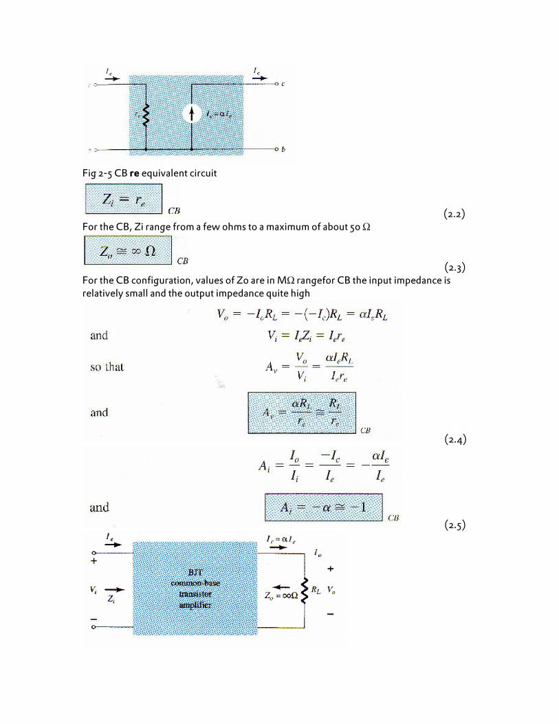
Fig 2-5 CB re equivalent circuit
(2.2) For the CB, Zi range from a few ohms to a maximum of about 50 Ω
(2.3) For the CB configuration, values of Zo are in MΩ rangefor CB the input impedance is relatively small and the output impedance quite high
(2.4)
(2.5)

Fig 2-6 Av=Vo/Vi for CB
Fig 2-7 approximate model for a CB npn transistor configuration Example 1: CB configuration with IE=4mA, =0.98, and an ac of 2mV applied between the base and emitter. Determine the Zi . Calculate Av if a load of 0.56kΩ is connected to the output terminals, find the Zo and Ai Solution:
Or
2.3 Common Emitter - Fixed bias configuration

Fig 2.8
2.3.1 Procedures for obtaining equivalent circuit
(i) Ac Equivalent circuit • Removing DC effects of VCC and Capacitors
Fig 2.9 (ii) equivalent re model
• Replace the transistor by its equivalent re model
Fig 2.10
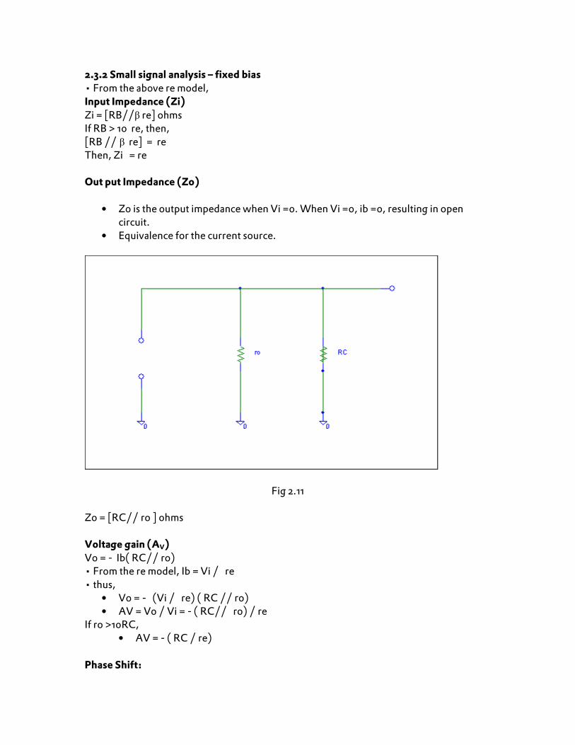
2.3.2 Small signal analysis – fixed bias • From the above re model, Input Impedance (Zi) Zi = [RB//β re] ohms If RB > 10 re, then, [RB // β re] = re Then, Zi = re Out put Impedance (Zo)
• Zo is the output impedance when Vi =0. When Vi =0, ib =0, resulting in open circuit.
• Equivalence for the current source.
Fig 2.11 Zo = [RC// ro ] ohms Voltage gain (AV) Vo = - Ib( RC// ro) • From the re model, Ib = Vi / re • thus,
• Vo = - (Vi / re) ( RC // ro) • AV = Vo / Vi = - ( RC// ro) / re
If ro >10RC, • AV = - ( RC / re)
Phase Shift:

The negative sign in the gain expression indicates that there exists 180o phase shift between the input and output
Fig 2.12
2.4 Common Emitter - Voltage-Divider Configuration
– Fig 2.13
2.4.1 equivalent re model
Fig 2.14

The re model is very similar to the fixed bias circuit except for RB is R1|| R2 in the case of voltage divider bias. • Expression for AV remains the same. Input impedance Zi = R1 ||R2|| re Output impedance Zo = RC Voltage Gain • From the re model, Ib = Vi / re • thus, Vo = - (Vi / re) ( RC || ro)
– • AV = Vo / Vi = - ( RC|| ro) / re If ro >10RC, AV = - (RC / re) Problem:2 Given: = 210, ro = 50k . Determine: re, Zi, Zo, AV. For the network given:
Fig 2.15
To perform DC analysis, we need to find out whether to choose exact analysis or
Approximate analysis. • This is done by checking whether RE > 10R2, if so, approximate analysis can be
chosen. • Here, RE = (210)(0.68k) = 142.8k . • 10R2 = (10)(10k) = 100k. • Thus, RE > 10R2.Therefore using approximate analysis.
VB = VccR2 / (R1+R2)

= (16)(10k) / (90k+10k) = 1.6V VE = VB – 0.7 = 1.6 – 0.7 = 0.9V IE = VE / RE = 1.324mA re = 26mV / 1.324mA = 19.64 Effect of ro can be neglected if ro 10( RC). In the given circuit, 10RC is 22k, ro is 50K. Thus effect of ro can be neglected. Zi = ( R1||R2|| RE) = [90k||10k||(210)(0.68k)] = 8.47k Zo = RC = 2.2 k AV = - RC / RE = - 3.24 If the same circuit is with emitter resistor bypassed, Then value of re remains same. Zi = ( R1||R2|| re) = 2.83 k Zo = RC = 2.2 k AV = - RC / re = - 112.02 2.5.Common Emitter - Unbypassed Emitter-Bias Configuration
Fig 2.16
2.5.1 re equivalent model
Fig 2.17
2.5.2 Small signal Analysis
Input impednce Applying KVL to the input side: Vi = Ib re + IeRE Vi = Ib re +( β +1) IbRE Input impedance looking into the network to the right of RB is Zb = Vi / Ib = re+ ( β +1)RE
Since β >>1, (β +1) = β
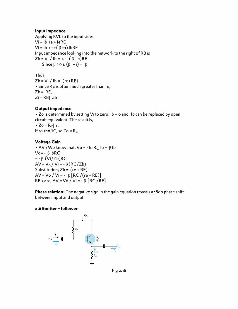
Thus, Zb = Vi / Ib = (re+RE) • Since RE is often much greater than re, Zb = RE, Zi = RB||Zb Output impedance • Zo is determined by setting Vi to zero, Ib = 0 and Ib can be replaced by open circuit equivalent. The result is, • Zo = RC||ro If ro >10RC, so Zo = RC Voltage Gain • AV : We know that, Vo = - Io RC, Io = β Ib Vo= - β IbRC = - β (Vi/Zb)RC AV = VO / Vi = - β (RC/Zb) Substituting, Zb = (re + RE) AV = Vo / Vi = - β [RC /(re + RE)] RE >>re, AV = Vo / Vi = - β [RC /RE] Phase relation: The negative sign in the gain equation reveals a 180o phase shift between input and output. 2.6 Emitter – follower
Fig 2.18

2.6.1 re equivalent model
Fig 2.19
Input Impedance Zi = RB || Zb • Zb = β re+ (β +1)RE • Zb = β (re+ RE) • Since RE is often much greater than re, Zb = β RE Output impedance • To find Zo, it is required to find output equivalent circuit of the emitter follower at its input terminal. • This can be done by writing the equation for the current Ib. Ib = Vi / Zb Ie = ( β +1)Ib = ( β +1) (Vi / Zb) • We know that, Zb = β re+ (β +1)RE substituting this in the equation for Ie we get, Ie = (β +1) (Vi / Zb) = (β +1) (Vi / β re+ (β +1)RE ) Ie = Vi / [ β re/ (β +1)] + RE • Since ( β +1) = β, Ie = Vi / [re + RE] • Using the equation Ie = Vi / [re + RE] , we can write the output equivalent circuit
as,
Fig 2.20
As per the equivalent circuit, Zo = RE||re

• Since RE is typically much greater than re, Zo = re •Voltage gain(AV): • Using voltage divider rule for the equivalent circuit, Vo = Vi RE / (RE+ re) AV = Vo / Vi = [RE / (RE+ re)] • Since (RE+ re) = RE, AV = [RE / (RE] = 1 Phase relationship
As seen in the gain equation, output and input are in phase.
Fig 2.21
Exercise 1: Derive the expression for Zi,Zo,Av,Ai of Common base configuration 2.7 Effect of RL and RS:
• Voltage gain of an amplifier without considering load resistance (RL) and source resistance (RS) is AVNL.
• Voltage gain considering load resistance ( RL) is AV < AVNL • Voltage gain considering RL and RS is AVS, where AVS<AVNL< AV • For a particular design, the larger the level of RL, the greater is the level of ac gain. • Also, for a particular amplifier, the smaller the internal resistance of the signal
source, the greater is the overall gain. 2.7.1Fixed bias with RS and RL:
Fig 2.22
AV = - (RC||RL) /β re Z i = RB|| β re

Zo = RC||ro To find the gain AVS, (Zi and RS are in series and applying voltage divider rule) Vi = VSZi / ( Zi+RS) Vi / VS = Zi / ( Zi+RS) AVS = Vo / VS = (Vo/Vi) (Vi/VS) AVS = AV [Zi / ( Zi+RS)] 2.7.2 Voltage divider with RS and RL
Fig 2.23
Voltage gain: AV = - [RC||RL] / βre Input Impedance: Zi = R1||R2|| βre Output Impedance: Zo = RC||RL|| βre 2.7.3 Emitter follower with RS and RL
re model:
Fig 2.24
Voltage Gain: AV = (RE||RL) / [RE||RL+ βre] Input Impedance: Zi = RB || Zb
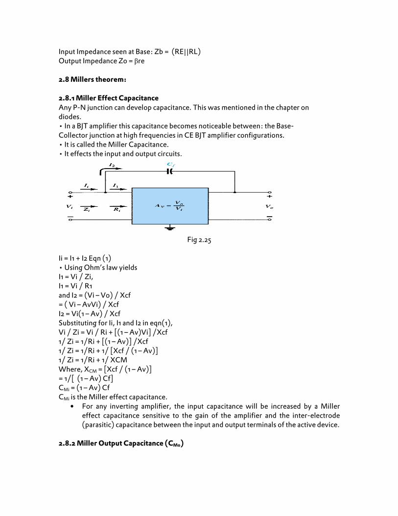
Input Impedance seen at Base: Zb = (RE||RL) Output Impedance Zo = βre 2.8 Millers theorem: 2.8.1 Miller Effect Capacitance Any P-N junction can develop capacitance. This was mentioned in the chapter on diodes. • In a BJT amplifier this capacitance becomes noticeable between: the Base- Collector junction at high frequencies in CE BJT amplifier configurations. • It is called the Miller Capacitance. • It effects the input and output circuits.
Fig 2.25
Ii = I1 + I2 Eqn (1) • Using Ohm’s law yields I1 = Vi / Zi, I1 = Vi / R1 and I2 = (Vi – Vo) / Xcf = ( Vi – AvVi) / Xcf I2 = Vi(1 – Av) / Xcf Substituting for Ii, I1 and I2 in eqn(1), Vi / Zi = Vi / Ri + [(1 – Av)Vi] /Xcf 1/ Zi = 1/Ri + [(1 – Av)] /Xcf 1/ Zi = 1/Ri + 1/ [Xcf / (1 – Av)] 1/ Zi = 1/Ri + 1/ XCM Where, XCM = [Xcf / (1 – Av)] = 1/[ (1 – Av) Cf] CMi = (1 – Av) Cf CMi is the Miller effect capacitance.
• For any inverting amplifier, the input capacitance will be increased by a Miller effect capacitance sensitive to the gain of the amplifier and the inter-electrode (parasitic) capacitance between the input and output terminals of the active device.
2.8.2 Miller Output Capacitance (CMo)

Fig 2.26
Applying KCL at the output node results in: Io = I1+I2 I1 = Vo/Ro and I2 = (Vo – Vi) / XCf The resistance Ro is usually sufficiently large to permit ignoring the first term of the equation, thus Io = (Vo – Vi) / XCf Substituting Vi = Vo / AV, Io = (Vo – Vo/Av) / XCf = Vo ( 1 – 1/AV) / XCf Io / Vo = (1 – 1/AV) / XCf Vo / Io = XCf / (1 – 1/AV) = 1 / wCf (1 – 1/AV) = 1/ wCMo CMo = ( 1 – 1/AV)Cf CMo = Cf [if |AV| >>1] If the gain (Av) is considerably greater than 1: CMo ≅ Cf

2.8.3 Relative Levels for the Important Parameters of the CE, CB, and CC Transistor Amplifier

SUMMARY Important Conclusions and Concepts

1. The re model for a BJT in the ac domain is sensitive to the actual dc operating conditions of the network. This parameter is normally not provided on a specification sheet, although hie of the normally provided hybrid parameters is equal to re but only under specific operating conditions. 2. Most specification sheets for BJT include a list of hybrid parameters to establish an ac model for the transistor. One must be aware, however, that they are provided for a particular set of dc operating conditions. 3. The CE fixed-bias configuration can have a significant voltage gain characteristic, although its input impedance can be relatively low. The approximate current gain is given by simply beta, and the output impedance is normally assumed to be Rc. 4. The voltage-divider bias configuration has a higher stability than the fixed-bias configuration, but it has about the same voltage gain, current gain, and output impedance. Due to the biasing resistors, its input impedance may be lower than that of the fixed-bias configuration. 5. The CE emitter-bias configuration with an unbypassed emitter resistor has a larger input resistance than the bypassed configuration, but it will have a much smaller voltage gain than the bypassed configuration. For the unbypassed or by-passed situation, the output impedance is normally assumed to be simply Rc. 6. The emitter-follower configuration will always have an output voltage slightly less than the input signal. However, the input impedance can be very large, making it very useful for situations where a high-input first stage is needed to "pick up "as much of the applied signal as possible. Its output impedance is extremely low, making it an excellent signal source for the second stage of a multistage amplifier. 7. The common-base configuration has very low input impedance, but it can have a significant voltage gain. The current gain is just less than 1, and the output impedance is simply Rc 8. The collector feedback configuration has input impedance that is sensitive to beta and that can be quite low depending on the parameters of the configuration. However, the voltage gain can be significant and the current gain of some magnitude if the parameters are chosen properly. The output impedance is most often simply the collector resistance Rc 9. The collector dc feedback configuration utilizes the dc feedback to increase its stability and the changing state of a capacitor from dc to ac to establish a higher voltage gain than obtained with a straight feedback connection. The output impedance is usually close to Rc and the input impedance relatively close to that obtained with the basic common-emitter configuration. 10. The approximate hybrid equivalent network is very similar in composition to that used with the re model. In fact, the same methods of analysis can be applied to both models. For the hybrid model the results will be in terms of the network parameters and the hybrid parameters, whereas for the re model they will be in terms of the network parameters and , re and ro 11. The hybrid model for common-emitter, common-base, and common-collector configurations is the same. The only difference will be the magnitude of the parameters of the equivalent network.

12. for BJT amplifiers that fail to operate properly, the first step should to be checking the dc level and be sure that they support the dc operation of the design. 13. Always keep in mind that capacitors are typically open circuits for the dc analysis and operation and essentially short circuits for the ac response. Equations CE fixed bias:
CE Voltage-divider bias:
CE emitter-bias:
Emitter-follower:
Common-base:

2.9 FET Small signal analysis

The gate-to-source ac voltage controls the drain-to-source (channel) current of an FET, Skockley's equation controlled the level of dc drain current through a relationship
[2.9.1] gm is a trans-conductance factor using to determined The change in Drain current that will result from a change in gate-to-source voltage in the following:
[2.9.2] Conductance of resistor g = 1/R = I/V
Graphical Determination of gm
[2.9.3]
Fig2.271Definition of gm using transfer curve Mathematical Definition of gm
The derivative of a function at a point is equal to the slope of the tangent line drawn at that point.
[2.9.4] The maximum value of gm for a JFET in which IDSS and VP have been specified
[2.9.5] 0 means the value of gm when VGS = 0 V, Eq[9-4] then becomes
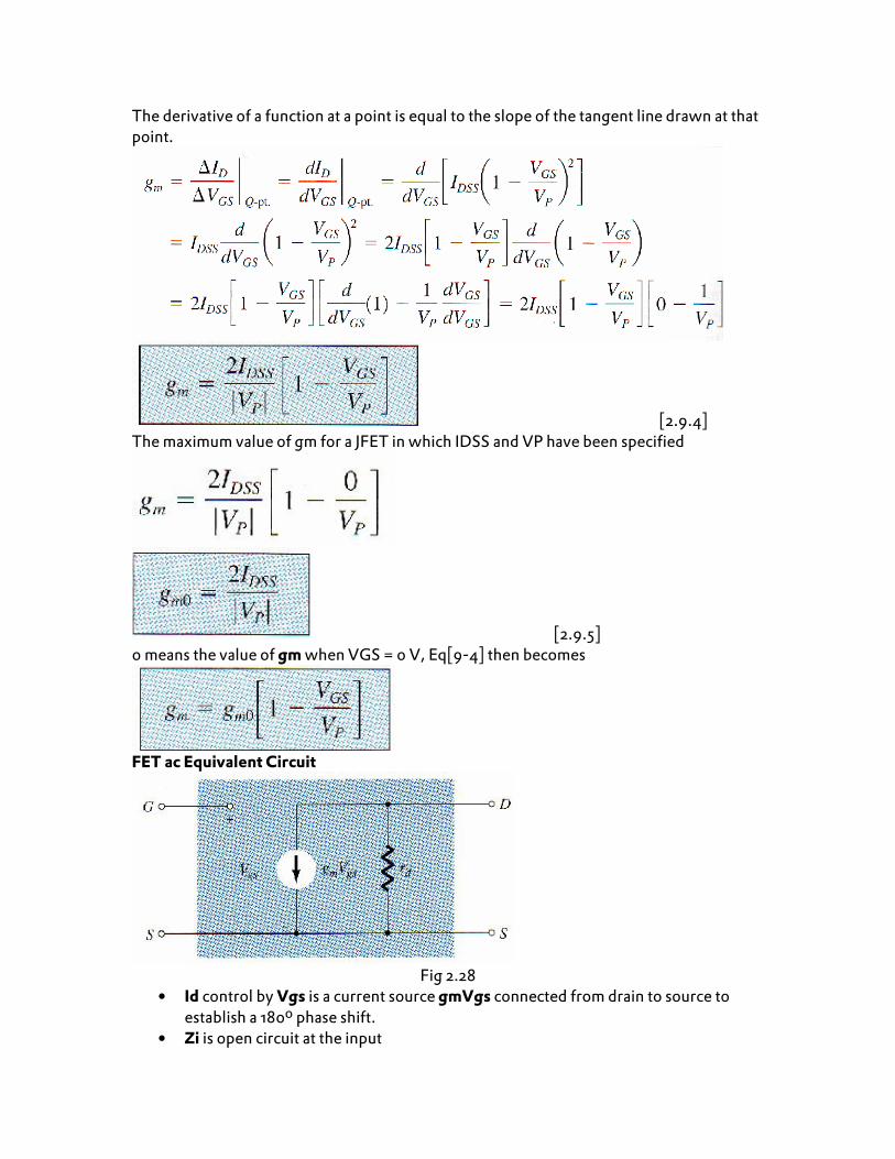
FET ac Equivalent Circuit
Fig 2.28
• Id control by Vgs is a current source gmVgs connected from drain to source to establish a 180º phase shift.
• Zi is open circuit at the input

• Zo is rd from drain to source Example 3: yfs =3.8mS and yos =20 S, Sketch the FET as equivalent model Solution:
2.9.1-JFET Fixed-Bias Configuration (Common-Source)
Fig 2.29 JFET fixed configuration Fig 2.30 JFET ac equivalent gm & rd determined from the dc biasing arrangement specification sheet, VGG & VDD are set to zero by a short circuit equivalent
[2.9.13]
Fig 2.31 Redrawn network
For obtaining ZO Setting Vi = 0V, will establish Vgs as 0V also, this result gmVgs = 0mA
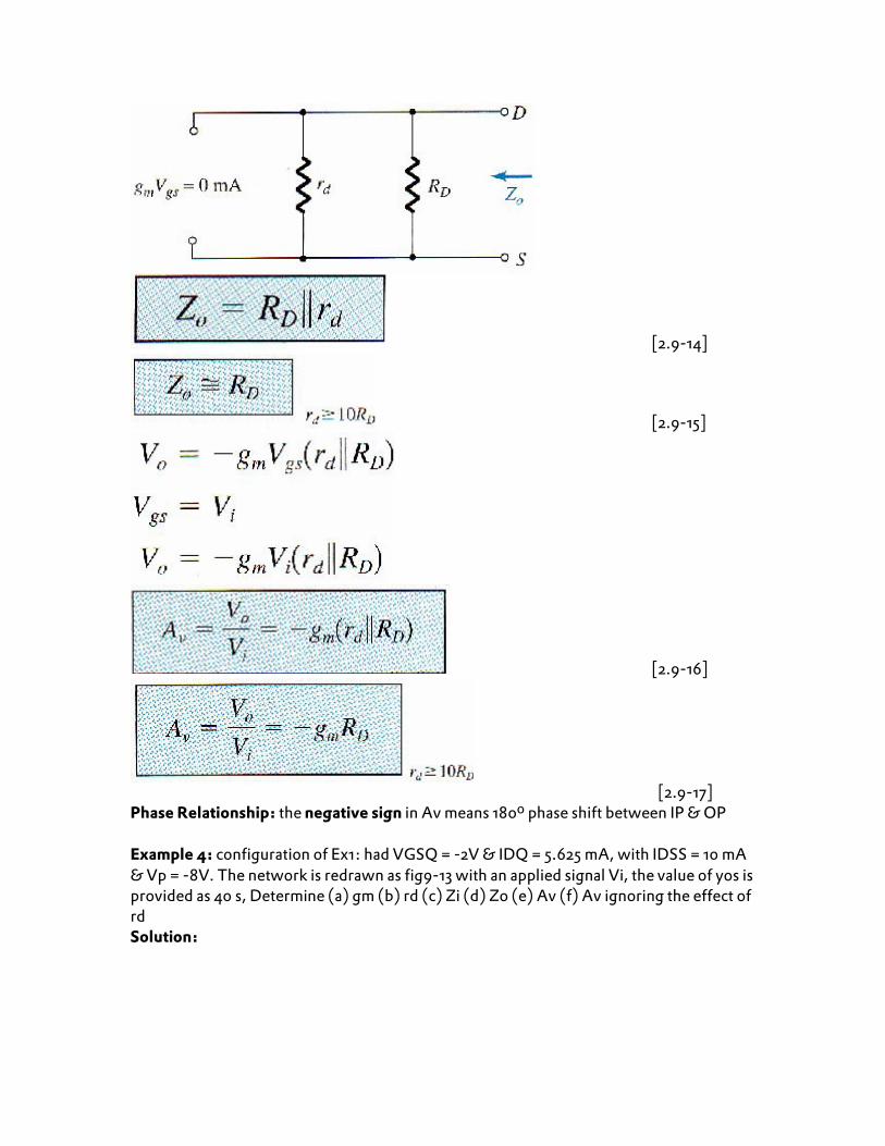
[2.9-14]
[2.9-15]
[2.9-16] [2.9-17]
Phase Relationship: the negative sign in Av means 180º phase shift between IP & OP Example 4: configuration of Ex1: had VGSQ = -2V & IDQ = 5.625 mA, with IDSS = 10 mA & Vp = -8V. The network is redrawn as fig9-13 with an applied signal Vi, the value of yos is provided as 40 s, Determine (a) gm (b) rd (c) Zi (d) Zo (e) Av (f) Av ignoring the effect of rd Solution:
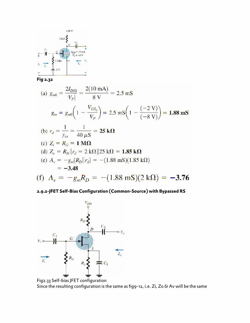
Fig 2.32
2.9.2-JFET Self-Bias Configuration (Common-Source) with Bypassed RS
Fig2.33 Self-bias JFET configuration Since the resulting configuration is the same as fig9-12, i.e. Zi, Zo & Av will be the same

Fig. 2.34 small signal equivalent circuit
[2.9-18]
[2.9-19]
[2.9-20]
[2.9-21]
[2.9-22] Phase Relationship: the negative sign in Av means 180º phase shift between IP & OP

2.9.3 JFET Self-Bias Configuration with Un-bypassed RS
Fig2.35 JFET with effect of RS with rd=∞Ω Due to the open-circuit condition between the gate and the output network, Zi
[2.9-23]
Setting Vi=0V will result in the gate terminal being at ground potential(0V).The voltage across RG is 0V, RG "shorted out" of the picture. Applying KCL will result
[2.9.24] If rd is included in the network, the equivalent will appear as shown in fig2.36

Fig2.36 rd effect in self-bias JFET
We try to find an expression for Io in terms of ID applying KCL:
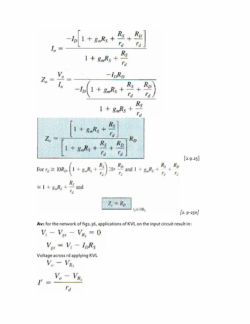
[2.9.25]
[2. 9-25a] Av: for the network of fig2.36, applications of KVL on the input circuit result in:
Voltage across rd applying KVL

Applying KCL will result
Substituting for Vgs from above and substituting for Vo and VRS we have
The output voltage Vo is
[2. 9-26]
[2.9-27] Phase Relationship: the negative sign in Av means 180º phase shift between IP & OP Example 5: configuration of fig2.37 has VGSQ=-2.6V & IDQ=2.6mA, with IDSS=8mA & VP=-6V.The network is redrawn as fig2.38 with an applied signal Vi. The value of yos is given as 20 S,Determine (a) gm (b) rd (c) Zi (d) Zo with and without rd (e) Av with and without rd.

Fig2.37 Fig2.38 Redrawn Solution:
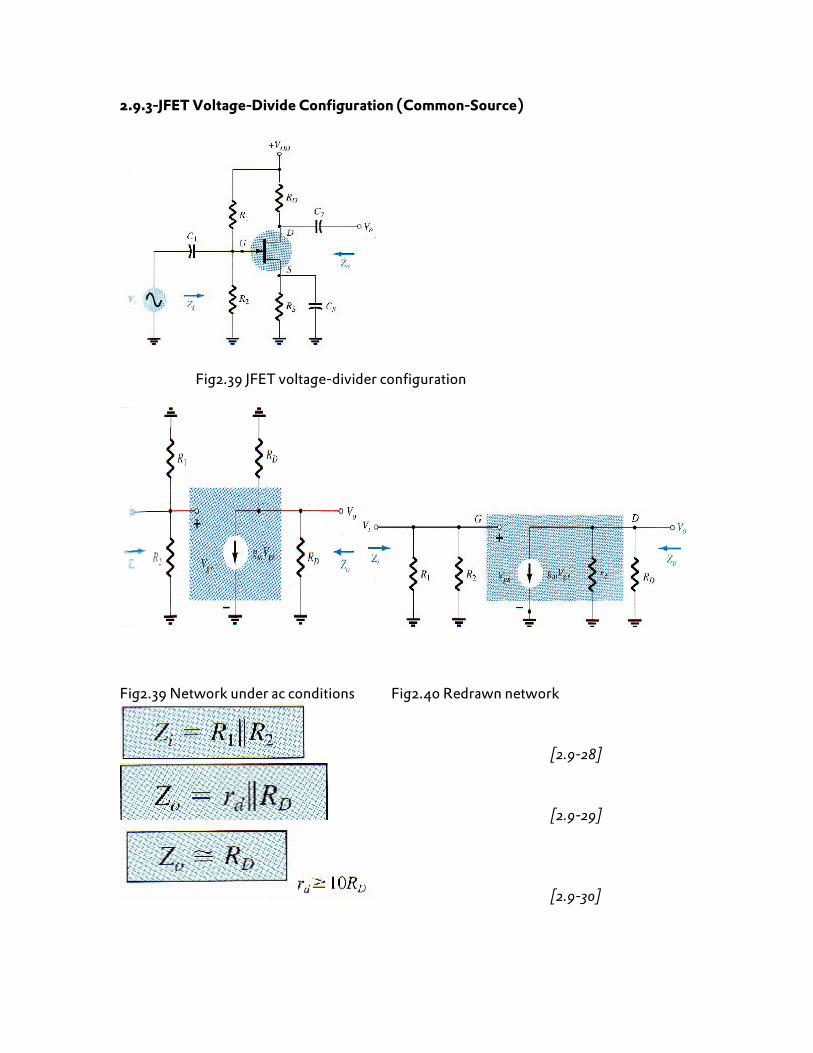
2.9.3-JFET Voltage-Divide Configuration (Common-Source)
Fig2.39 JFET voltage-divider configuration
Fig2.39 Network under ac conditions Fig2.40 Redrawn network
[2.9-28]
[2.9-29]
[2.9-30]

[2.9-31]
[2.9-32] 2.9.4 JFET Source-Follower (Common-Drain Configuration) The output is taken off the source terminal and when the dc supply is replaced by it's short-circuit equivalent, the drain is grounded (hence, the terminology common-drain)
Fig2.41 JFET Source-Follower configuration Fig2.42 JFET ac equivalent model
Fig2.43 redrawn the network

` [2.9-33] Setting Vi = 0V will result in the gate terminal being connected directly to ground so that Zo=
Fig2.44
Vo= -Vgs applying KCL at node S

[2.9-34]
[2.9-35]
Applying KVL around the perimeter of the network of fig9-26 will result in:
[9-36]
[2.9-37] Since the bottom of Eq[2.9-37] is larger than the numerator by a factor of one, the gain can never be equal to or greater than one. Phase Relationship: since Av is a positive quantity, Vo and Vi are in phase

Summary Table

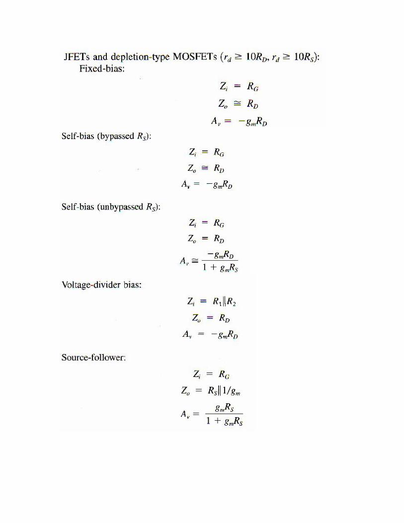
Summary Important Conclusion and Concept 1- The trans-conductance parameter gm is determined by the ratio of the change in drain current associated with a particular change in gate-to-source voltage 2- On specification sheets, gm is provided as yfs 3-When VGS is one-half the pinch-off value; gm is one-half the maximum value 4- When ID is one-fourth the saturation level of IDSS , gm is one-half the value at saturation 5- The output impedance of FETs is similar in magnitude to that of conventional BJTs 6- On specification sheets the output impedance rd is provided as 1/ yos . 7- The voltage gain for the fixed-bias and self-bias JFET configurations (with a by passed source capacitance) is the same. 8- The ac analysis of JFETs and depletion-type MOSFETs is the same. 9- The ac equivalent network for E-MOSFETs is the same as that employed for the JFETs and D-MOSFETs, the only difference is the equation for gm 10- The magnitude of the gain of FET networks is typically between 2 and 20. The self-bias configuration (without a bypass source capacitance) and the source follower are low-gain configurations 11- There is no phase shift between input and output for the source-follower 12- The output impedance for most FET configurations is determined primarily by RD For the source-follower configuration it is determined by RS and gm. Equations
2.10 DIFFERENTIAL AMPLIFIERS OBJECTIVES
• The basic idea of the differential pair. • The benefits of the differential pair (no coupling caps -> DC response, etc.). • DC operation of the differential pair. • The basic small-signal equivalent circuit for the differential pair. • Common-mode operation of the differential pair. • The frequency response of the differential pair. • Non-ideal properties of the differential pair. •
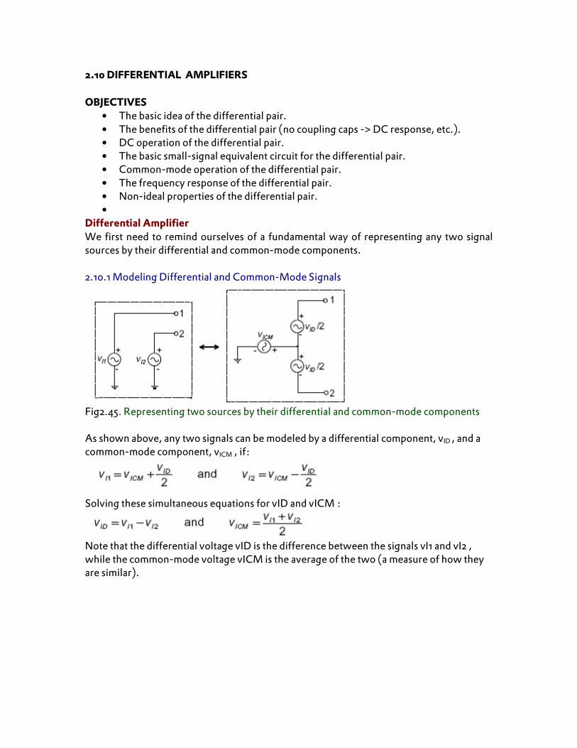
Differential Amplifier We first need to remind ourselves of a fundamental way of representing any two signal sources by their differential and common-mode components. 2.10.1 Modeling Differential and Common-Mode Signals
Fig2.45. Representing two sources by their differential and common-mode components As shown above, any two signals can be modeled by a differential component, vID , and a common-mode component, vICM , if:
Solving these simultaneous equations for vID and vICM :
Note that the differential voltage vID is the difference between the signals vI1 and vI2 , while the common-mode voltage vICM is the average of the two (a measure of how they are similar).

2.10.2 DIFFERENTIAL AMPLIFIER BASIC CONCEPTS
The differential amplifier circuit (as shown above, it is often referred to as a differential pair) is the basis for any operational amplifier (you can find one on the input of nearly any op-amp type chip). The two transistors are ideally identical and are generally assumed to be below
. Fig2.46
• There are two inputs, v1 and v2 , and one can apply inputs to both (differentially) or ground one and use the amplifier in a single-ended (ground referenced) way.
• This circuit can compute the difference between two input signals. • While the op-amp symbol ("triangle") has only one output, the differential pair
shown above has two (vo1 and vo2). One can take outputs from both (differentially) or use just one relative to ground (as you would with a typical op-amp).
• The differential pair is basically two common emitter amplifiers sharing a common current source that sets the total DC bias current through both transistors at 2IE.
• In seeking to understand its operation, we will begin by looking at the shifting of this DC current between the two transistors when there is a large-signal imbalance between their two inputs (i.e. the difference between v1 and v2 is large).
• With NO differential signal input (v1 and v2 are the same), the current flowing out the emitter of each transistor is IE and therefore, vo1 = vo2 in this situation (if RC1 = RC2, which is usually the case). • For the small-signal case, if the collector currents are the same in both transistors (IE IC), their gm's and other parameters will be equal (both transistors are as close to identical as possible).
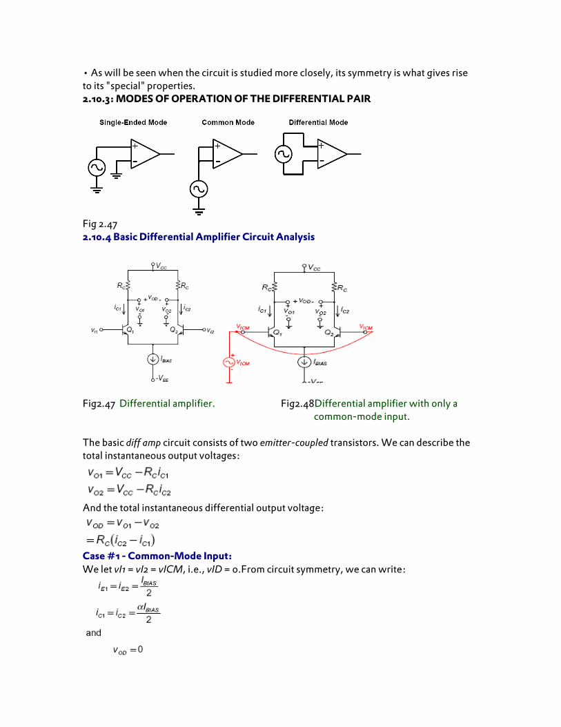
• As will be seen when the circuit is studied more closely, its symmetry is what gives rise to its "special" properties. 2.10.3: MODES OF OPERATION OF THE DIFFERENTIAL PAIR
Fig 2.47 2.10.4 Basic Differential Amplifier Circuit Analysis
Fig2.47 Differential amplifier. Fig2.48Differential amplifier with only a
common-mode input. The basic diff amp circuit consists of two emitter-coupled transistors. We can describe the total instantaneous output voltages:
And the total instantaneous differential output voltage:
Case #1 - Common-Mode Input: We let vI1 = vI2 = vICM, i.e., vID = 0.From circuit symmetry, we can write:

Case #2A - Differential Input:
Fig2.49 Differential amplifier with +2 V differential input . Now we let vID = 2 V and vICM = 0.Note that Q1 is active, but Q2 is cutoff. Thus we have:
Case #2B - Differential Input:
Fig2.50 Differential amplifier with - 2 V differential input This is a mirror image of Case #2A. We have vID = -2 V and vICM = 0.
Now Q2 is active and Q1 cutoff:
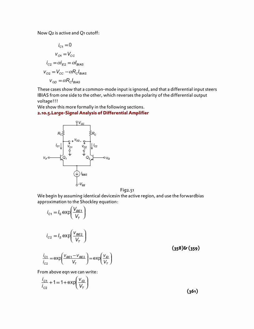
These cases show that a common-mode input is ignored, and that a differential input steers IBIAS from one side to the other, which reverses the polarity of the differential output voltage!!! We show this more formally in the following sections. 2.10.5.Large-Signal Analysis of Differential Amplifier
Fig2.51
We begin by assuming identical devicesin the active region, and use the forwardbias approximation to the Shockley equation:
(358)& (359)
From above eqn we can write:
(361)
And we can also write:
(362) Equating (361) and (362) and solving for iC2 :
(363) To find a similar expression for iC1 we would begin by dividing eqn. (359) by (358) . . . the result is:
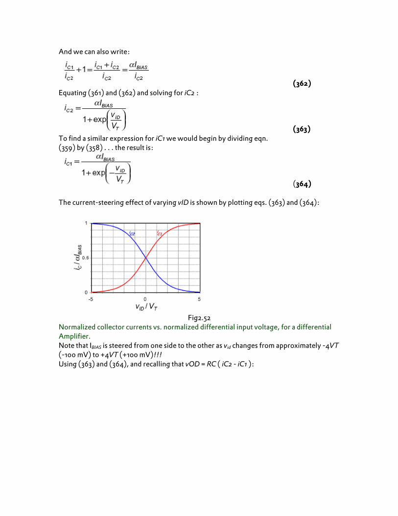
(364) The current-steering effect of varying vID is shown by plotting eqs. (363) and (364):
Fig2.52
Normalized collector currents vs. normalized differential input voltage, for a differential Amplifier. Note that IBIAS is steered from one side to the other as vid changes from approximately -4VT (-100 mV) to +4VT (+100 mV)!!! Using (363) and (364), and recalling that vOD = RC ( iC2 - iC1 ):

• Thus we see that differential input voltage and differential output voltage are
related by a hyperbolic tangent function!!! • A normalized version of the hyperbolic tangent transfer function is plotted below:
Fig 2.53. Normalized differential output voltage vs normalized differential input voltage,
for a differential amplifier. • This transfer function is linear only for |vID /VT| much less than 1,i.e., for |vID| much
less than 25 mV!!! • We usually say the transfer function is acceptably linear for a |vID| of 15 mV or less. • If we can agree that, for a differential amplifier, a small input signal is less than
about 15 mV, we can perform a small-signal analysis of this circuit !!!
2.10.6 Small-Signal Analysis of Differential Amplifier 2.10.6.1 Differential Input Only
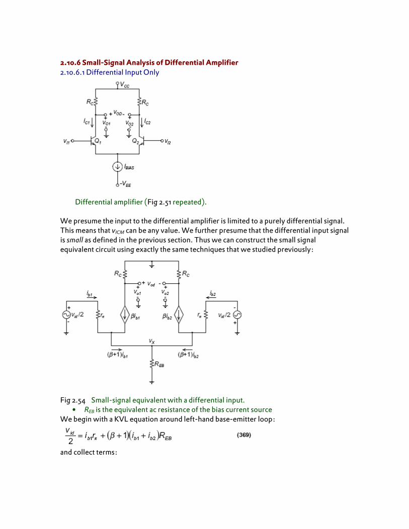
Differential amplifier (Fig 2.51 repeated). We presume the input to the differential amplifier is limited to a purely differential signal. This means that vICM can be any value. We further presume that the differential input signal is small as defined in the previous section. Thus we can construct the small signal equivalent circuit using exactly the same techniques that we studied previously:
Fig 2.54 Small-signal equivalent with a differential input.
• REB is the equivalent ac resistance of the bias current source We begin with a KVL equation around left-hand base-emitter loop:
and collect terms:

We also write a KVL equation around right-hand base-emitter loop:
and collect terms:
Adding (370) and (372):
Because neither resistance is zero or negative, it follows that
and, because vX = (ib1 + ib2)REB , the voltage vX must be zero, i.e., point X is at signal ground for all values of REB !!! The junction between the collector resistors is also at signal ground, so the left half-circuit and the right half-circuit are independent of each other, and can be analyzed separately !!! 2.10.7 Analysis of Differential amplifier using Bisection theorem( Half-Circuit concept)
Fig 2.55
Left half-circuit of differential amplifier with a differential input.The circuit at left is just the small signal equivalent of a common emitter amplifier, so we may write the gain equation directly:
For vo1/vid we must multiply the denominator of eq. (375) by two:

In the notation Avds the subscripts mean: v, voltage gain d, differential input s, single-ended output The right half-circuit is identical to Fig. 332, but has an input of -vid /2, so we may write:
Finally, because vod = vo1 - vo2, we have the result:
where the subscript b refers to a balanced output. Thus, we can refer to differential gain for either a single-ended output or a differential output.
Diff. amp. small-signal equivalent (Fig 2.54repeated) Eq. (378) is just the slope of that function, evaluated at vID = 0 !!! Other parameters of interest . . . Differential Input Resistance This is the small-signal resistance seen by the differential source:
Differential Output Resistance This is the small-signal resistance seen by the load, which can be single-ended or balanced. We can determine this by inspection:

2.10.8 Common-Mode Input Only
Fig 2.56 Differential amplifier Small-signal equivalent with a common-mode input. The resistance of the bias current source is represented by
We now restrict the input to a common-mode voltage only. This is, we let vID = 0. We again construct the small-signal circuit using the techniques we Studied previously. As a bit of a trick, we represent the current source as two resistors in series:
Small-signal equivalent with a common-mode input.(fig repeated) Note the current iX . The voltage across each 2REB resistor is identical because the resistors are connected across the same nodes. Therefore, the current iX is zero and we can remove the connection between the resistors !!! This “decouples” the left half-circuit from the right half-circuit at the emitters. At the top of the circuit, the small-signal ground also decouples the left half-circuit from the right half-circuit.
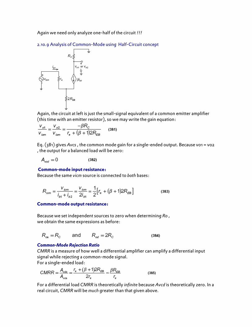
Again we need only analyze one-half of the circuit !!! 2.10.9 Analysis of Common-Mode using Half-Circuit concept
Again, the circuit at left is just the small-signal equivalent of a common emitter amplifier (this time with an emitter resistor), so we may write the gain equation:
Eq. (381) gives Avcs , the common mode gain for a single-ended output. Because vo1 = vo2 , the output for a balanced load will be zero:
Common-mode input resistance: Because the same vicm source is connected to both bases:
Common-mode output resistance: Because we set independent sources to zero when determining Ro , we obtain the same expressions as before:
Common-Mode Rejection Ratio
CMRR is a measure of how well a differential amplifier can amplify a differential input signal while rejecting a common-mode signal. For a single-ended load:
For a differential load CMRR is theoretically infinite because Avcd is theoretically zero. In a real circuit, CMRR will be much greater than that given above.

To keep these two CMRRs in mind it may help to remember the following:
• Avcs = 0 if the bias current source is ideal (for which REB = ∞). • Avcd = 0 if the circuit is symmetrical (identical left- and righthalves).
CMRR is almost always expressed in dB: