Embed Size (px)
Citation preview

ADC08D1000,ADC08D1500,ADC10DL065,ADC12DL040,ADC12DL065,ADC12QS065,LMH6550,LMH6551,LMH6703
Understanding High-Speed Signals, Clocks, and Data Capture
Literature Number: SNAA121

Feature Article ..........1-7
Medical Imaging Solution ..........................2
Test and MeasurementSolution ......................4-5
Design Tools ..................8
SIGNAL PATH designer SM
Tips, tricks, and techniques from the analog signal-path experts
As today’s data conversion sample rates for analog-to-digital converters are moving into the Giga Samples Per Second (GSPS) range, systems need to be capable of such high conversion rates and the supporting
analog components have to generate and amplify high-frequency signals. Inaddition to the analog signal path, the circuit areas that the designer shouldthoroughly understand are the sampling clock and the capturing of digital dataat high bit rates. This issue of the Signal Path Designer will provide suggestedsolutions for these two key areas. The following information is particularly relevant for systems that require high-performance ADCs.
Clock Sources One of the most important sub-circuits within a high-speed data conversionsystem is the clock source. This is because the timing accuracy of the clock sig-nal can directly affect the dynamic performance of the ADC. To minimize thisinfluence, an ADC clock source must exhibit very low levels of timing jitter orphase noise. If this factor is not considered when choosing a clock circuit, thesystem could deliver poor dynamic performance irrespective of the quality ofthe front-end analog input circuitry or ADC. A perfect clock will always deliver edge transitions at precise time intervals. In practice, clock edges willarrive at continuously varying intervals. As a result of this timing uncertainty,
Understanding High-Speed Signals,Clocks, and Data Capture — By Ian King, Applications Engineer
No. 103
NEXT ISSUE:
Precision Sensor Interface
Poor ClockFrequency Spectrum
Good ClockFrequency Spectrum
Frequency Frequency
Am
plitu
de
Am
plitu
de
Figure 1. Examples of Clock Signal Spectral Analysis
8203_Signal_Path_103 10/17/05 14:52 Page 1

High-Performance Solutions for Medical Imaging
Simplified Positron-Emission Tomography (PET) Scanner Block Diagram
VGAs
Quad Amp Quad ADC
PhotoMultiplierOutputs
ScintillationCrystals
SummingAmp
Comparator
FPGA
Product ID TypeSSBW (MHz, Av = 1)
Slew Rate(V/µs, Av=1)
ICC
(mA/ch)
2nd/3rd HD (dBc, VOUT = 2 VPP)
Voltage Noise
(nV/ Hz)Package
LMH6550 Fully differential ADC driver w/ disable 400 3000 20.0 -92 / -103 at 5 MHz, RL=800Ω 6.0 SOIC-8, MSOP-8
LMH6551 Fully differential ADC driver 370 2400 12.5 -94 / -96 at 5 MHz, RL=800Ω 6.0 SOIC-8, MSOP-8
LMH6703 1.2 GHz low distortion op amp w/shutdown 1.2 GHz2 42002 11.0 -69 / -90 at 20 MHz, RL=100Ω 2.3 SOIC-8, SOT23-6
LMH6502 Linear in dB, variable gain amplifier 1301 18001 27.0 -55 / -57 at 20 MHz, RL=100Ω 7.7 SOIC-14, TSSOP-14
LMH6503 Linear in V/V, variable gain amplifier 1351 18001 37.0 -60 / -61 at 20 MHz, RL=100Ω 6.6 SOIC-14, TSSOP-14
LMH6504 Linear in dB, variable gain amplifier 1501 15001 11.0 -47 / -55 at 20 MHz, RL=100Ω 4.4 SOIC-8, MSOP-8
LMH6722 Quad wideband, low power op amp 400 1800 5.6 -72 / -85 at 5 MHz, RL=100Ω 3.4 SOIC-14
LMH6725 Quad, ultra low power op amp 370 6002 1.0 -65 / -63 at 5MHz, RL=100Ω 4.3 SOIC-14, TSSOP-14
Product ID Type Response Time (ns)
Rise/Fall Times
ICC(mA/ch) CMVR Output
Config Package
LMV7219 7 ns, 2.7V to 5V comparator w/ RRO 7 1.3 ns 1.1 -0.2V to 3.8V Push-pull SC70-5, SOT23-5
NEW!
NEW!
NEW!
2
1 Av = +10 2 Av = +2
High-Speed Amplifiers and Comparators for Medical Imaging
Product ID Resolution Speed(MSPS)
Supply Voltage (V)
Power (mW)
SFDR (dB)
THD (dB)
ENOB (bit)
SNR (dB) Package
ADC10065 10 bit 65 3 68.4 80 -72 9.5 59 TSSOP-28ADC10080 10 bit 80 3 78.6 79 -75 9.5 59 TSSOP-28ADC10DL065 10-bit dual 65 3.3 360 80 -78 9.8 61 TQFP-64ADC12DL040 12-bit dual 40 3 210 86 -83 11.1 69 TQFP-64ADC12DL065 12-bit dual 65 3.3 360 86 -84 11.1 69 TQFP-64ADC12QS065 12-bit quad 65 3 800 85 -83 11.0 69 TQFP-64, LLP-60ADC14L020 14 bit 20 3.3 150 92 90 12.0 74 LQFP-32ADC14L040 14 bit 40 3.3 236 90 87 11.9 73 LQFP-32
High-Speed ADCs for Medical Imaging Dynamic Performance
NEW!
NEW!
NEW!
8203_Signal_Path_103 10/17/05 14:52 Page 2

the signal-to-noise ratio of a sampled waveform canbe compromised by the data conversion process.
The maximum clock jitter that can be tolerated fromall jitter sources before the noise due to jitter exceedsthe quantization noise (1/2 LSB). This is definedfrom the following equation:
Tj(rms) = (VIN(p-p) / VINFSR) x (1/(2(N+1) x π x fin))
If the Input Voltage (VIN) is optimized to equal thefull scale range of the ADC (VINFSR), then the jit-ter requirement becomes a factor of the ADC’s res-olution (N bits) and the input frequency beingsampled (fin).
For input frequencies up to the Nyquist rate (500 MHz for a 1 GSPS conversion rate), the totaljitter requirement would be:
Tj(rms) = 1 x (1/(2(8+1) x π x 500 x 106))
Tj(rms) = 1.2 ps
This value represents the total jitter from allsources. A source of jitter that can be accounted forwithin the ADC device itself is called the aperturejitter. This is a timing uncertainty associated withthe input sample and hold circuit of the device andshould be considered when determining the maxi-mum allowable clock jitter of the clock source.
Clock Circuit Jitter = SQRT (Tj(rms)
2 – (ADC Aperture Jitter)2 )
Using the ADC08D1000 as an example, the aperture jitter is given in the datasheet as 0.4 ps,this value tightens the jitter specification for theADC clock to ~1.1 ps.
However, simply matching an oscillator’s perform-ance data to the requirements specification may notbe enough to obtain the expected result when usedin the data conversion system. This is because frequency components that exist alongside the fundamental also play a significant role. It is there-fore important to examine the clock signal with aspectrum analyzer and make sure that the energyassociated with the fundamental frequency is notspread over too wide a range. Spurs that extend tohigher frequencies may be visible and will also havea direct impact on jitter performance. Figure 1 compares an example of a poor performance clocksignal alongside the frequency spectrum that wouldbe expected from a good, clean low-jitter clocksource.
Figure 2 shows the recommended clock circuit forthe ADC08D1000. It consists of a Phase LockedLoop (PLL) device (LMX2312) connected to aVari-L Voltage Controlled Oscillator (VCO).
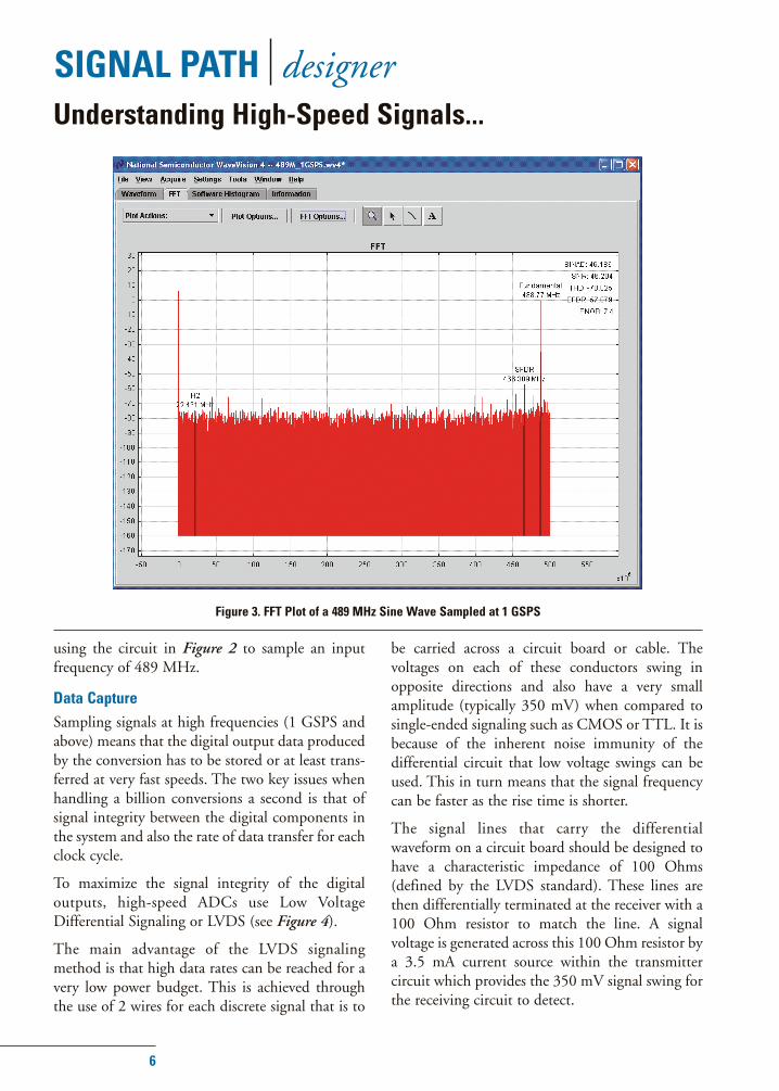
The PLL and VCO maintains the required signalto noise ratio (46 dB) for the ADC08D1000 product up to the Nyquist input frequency. TheFFT plot in Figure 3 shows the dynamic performance of the ADC when clocked at 1 GSPS
Understanding High-Speed Signals...
SIGNAL PATH designer
NC11121314151617
18 19 20
1234567
8910
DATALEGNDCEVucNC VC
C
NC
NC
CPoGND
FinFinb
FL Vp
OSCinCLOC
KFo
LDOS
Cout
V uc
10Ω
10 pF10 pF
680Ω
GNDVtGNDGND
GN
D
GND
GND
MO
DG
ND
GND
GN
DG
ND
VCC
GN
DG
ND
VCC
4.7 nF
100Ω
100 pF
270Ω 270Ω
18Ω
10Ω
470 pF
10 kΩ
100 pF27 nF
2.7 kΩ
470 pF100 pF
1500 pF
VCC18Ω
18Ω10 nF10 nF
LMX2312
Vari -LVCO190
SERIAL_CLOCK
SERIAL_DATA
DATA_LATCH
CHIP_ENABLE
RF_OUT
4.7 nF
ADC CLK+
ADC CLK–
100 pF
Figure 2. PLL and VCO Clock System3
8203_Signal_Path_103 10/17/05 14:52 Page 3

4
Coarseattenuator
Coarseattenuator
Amp
Amp 8-bit ADC
8-bit ADC Data memory
Data memory
LCD monitor
LCD driver
CPU
Timing controller
Triggercontrol
Display memory
Clock generator
Time base
LPfilter
LPfilter
Fineattenuator
Fineattenuator
ADC08D1500
Signal-Path Solutions for Test and Measurement
Simplified Oscilloscope
8-bit 1-3 GSPS ADC Family Performance (typical)• 7.3 to 7.5 Effective Number of Bits (ENOB) at Nyquist• 1.75 GHz full power bandwidth• Bit error rate 10-18
• DNL ±0.25 LSB• Crosstalk -71 dB
• Operating power of only 1W to 1.8W (no heat sink required)
Features• Interleaved dual-edge sampling (DES) mode enables up to
3.4 GSPS operation• Choice of single or dual data rate output clocking• Multiple ADC synchronization capability• Serial interface for extended control (gain, offset)• Demultiplexed LVDS outputs simplify data capture
Product ID Description
ADC081000 8-Bit, 1 GSPS
ADC081500 8-Bit, 1.5 GSPS
ADC08D500 8-Bit, dual, 500 MSPS (1 GSPS in DES mode)
ADC08D1000 8-Bit, dual, 1 GSPS (2 GSPS in DES mode)
ADC08D1500 8-Bit, dual, 1.5 GSPS (3 GSPS in DES mode)
I Input, 2 GSPS Interleaved Operation2 nS/div
Step Response
BP FilterPLL
VCO
LMX231xADCclk Balun
Clock Generator
8203_Signal_Path_103 10/17/05 14:52 Page 4

5
Mixer
IF FilterIF Amplifier
Local Oscillator
Analog Signal Processing
ADC
Digital Signal Processing
Simplified Receiver Path
Product ID Type SSBW (MHz, Av = 1)
Slew Rate(V/µs, Av=1)
ICC(mA/ch)
2nd/3rd HD (dBc, VOUT = 2 VPP)
Voltage Noise
(nV / Hz)Package
LMH6550 Fully differential ADC driver with disable 400 3000 20.0 -92 / -103 at 5 MHz, RL=800Ω 6.0 SOIC-8, MSOP-8
LMH6551 Fully differential ADC driver 370 2400 12.5 -94 / -96 at 5 MHz, RL=800Ω 6.0 SOIC-8, MSOP-8
LMH6702 Ultra-low distortion CFB op amp 1.7 GHz1 31001 12.5 -100 / -96 at 5 MHz, RL=100Ω 1.8 SOIC-8, SOT23-5
LMH6703 1.2 GHz low distortion op amp w/shutdown 1.2 GHz1 42001 11.0 -87/ -100 at 5 MHz, RL=100Ω 2.3 SOIC-8, SOT23-6
LMH6609 900 MHz, unity gain stable, VFB op amp 900 1400 7.0 -87 / -82 at 5 MHz, RL=100Ω 3.1 SOIC-8, SOT23-5
LMH6574 4:1 Mux, -70 dB crosstalk 5001 2200 13.0 -65 / -86 at 5 MHz, RL=100Ω 5.0 SOIC-14
Product ID Type Response Time (ns)
Rise/Fall Times
ICC(mA/ch) CMVR Output
Config Package
LMV7219 7 ns, 2.7V to 5V comparator w/ RRO 7 1.3 ns 1.1 -0.2V to 3.8V Push-pull SC70-5, SOT23-5
NEW!
NEW!
NEW!
1 Av = +2
Applications:
• Spectrum analyzer• Radar system• Microwave links• Wireless infrastructure
Product ID Resolution Speed(MSPS)
Supply Voltage (V)
Power (mW)
SFDR (dB)
THD (dB)
ENOB (bit)
SNR (dB) Package
ADC08D1000 8-bit dual 1000 1.9 1600 55 -55 7.4 47 LQFP-128 Exp. PadADC08D1500 8-bit dual 1500 1.9 1840 53 -53 7.3 46 LQFP-128 Exp. PadADC10DL065 10-bit dual 65 3.3 360 80 -78 9.8 61 TQFP-64ADC12L080 12 bit 80 3.3 425 80 -77 10.7 66 LQFP-32ADC12DL040 12-bit dual 40 3 210 86 -83 11.1 69 TQFP-64ADC12DL065 12-bit dual 65 3.3 360 86 -84 11.1 69 TQFP-64ADC12QS065 12-bit quad 65 3 800 85 -83 11.0 69 TQFP-64, LLP-60ADC14L040 14 bit 40 3.3 236 90 87 11.9 73 LQFP-32
ADCs for Test and Measurement
Local Oscillator PLLatinumTM Frequency Synthesizers
Amplifiers and Comparators for Test and Measurement
Dynamic Performance
NEW!
NEW!
NEW!
NEW!
NEW!
NEW!
Product ID Type FrequencyNormalized
Phase NoisePhase Noise at
Offset FrequencyPackage
LMX2434 High Frequency Integer-N Dual PLL 1.0 - 5.0 GHz -219 dBc/Hz – UTCSP-20, TSSOP-20
LMX2430 Integer-N Dual PLL 0.2 - 3.0 GHz -219 dBc/Hz – UTCSP-20, TSSOP-20
LMX2470 Delta-Sigma Fractional-N PLL 0.5 - 2.6 GHz -210 dBc/Hz – UTCSP-24
LMX2364 Fractional-N PLL 0.5 - 2.6 GHz -210 dBc/Hz – UTCSP-24, TSSOP-24
LMX2347 Integer-N Single PLL 0.2 - 2.5 GHz -217 dBc/Hz – CSP-16, TSSOP-16
LMX2512 Frequency Synthesizer System with Integrated VCO ~ 1.0 GHz – -139 dBc/Hz at 900 kHz LLP-28
8203_Signal_Path_103 10/17/05 14:52 Page 5
6
using the circuit in Figure 2 to sample an input frequency of 489 MHz.
Data CaptureSampling signals at high frequencies (1 GSPS andabove) means that the digital output data producedby the conversion has to be stored or at least trans-ferred at very fast speeds. The two key issues whenhandling a billion conversions a second is that ofsignal integrity between the digital components inthe system and also the rate of data transfer for eachclock cycle.
To maximize the signal integrity of the digital outputs, high-speed ADCs use Low VoltageDifferential Signaling or LVDS (see Figure 4).
The main advantage of the LVDS signalingmethod is that high data rates can be reached for avery low power budget. This is achieved throughthe use of 2 wires for each discrete signal that is to
be carried across a circuit board or cable. The voltages on each of these conductors swing inopposite directions and also have a very smallamplitude (typically 350 mV) when compared tosingle-ended signaling such as CMOS or TTL. It isbecause of the inherent noise immunity of the differential circuit that low voltage swings can beused. This in turn means that the signal frequencycan be faster as the rise time is shorter.
The signal lines that carry the differential waveform on a circuit board should be designed tohave a characteristic impedance of 100 Ohms(defined by the LVDS standard). These lines arethen differentially terminated at the receiver with a100 Ohm resistor to match the line. A signal voltage is generated across this 100 Ohm resistor bya 3.5 mA current source within the transmitter circuit which provides the 350 mV signal swing forthe receiving circuit to detect.
Understanding High-Speed Signals...
SIGNAL PATH designer
Figure 3. FFT Plot of a 489 MHz Sine Wave Sampled at 1 GSPS
8203_Signal_Path_103 10/17/05 14:52 Page 6

7
Transmitting the data at high speeds is only half ofthe problem. Storing the data into a memory arrayfor post processing is also to be considered. The ADCprovides a de-multiplexed data output for each of itstwo channels. Instead of providing a single 8-bit busrunning at a data rate equal to the sample rate, thedevice outputs two consecutive samples simultane-ously on two 8-bit data buses. This method reducesthe data rate by a half but increases the number ofbits. For a 1 GSPS sample rate, the conversion dataoutput from the ADC is 500 MHz. Even at thisreduced speed, most discrete or internal FPGA memories would have problems capturing this datareliably. It is therefore beneficial to use a Dual DataRate (DDR) method where data is presented to theoutputs on both the rising and falling edges of theclock. While the data rate remains the same for DDRsignaling, the clock frequency is halved again to amore manageable 250 MHz. This frequency is nowin the realm of CMOS memory circuits. Before thedata can be stored to memory, it requires an interme-diate pair of data latches at the input to the FPGAdevice. The first latch of the pair is clocked using anin-phase data clock, while the second latch is clockedusing a signal that is 180 degrees out of phase or aninverted data clock (see Figure 5).
To simplify this clocking requirement, FPGAs comeequipped with digital clock managers in the form ofPLLs (Phase Locked Loop) or DLLs (Delay LockedLoop). These devices allow clock signals to be generated internally that are phase locked to an inputclock, and offer phase delay taps of 0, 90, 180, and270 degrees. This clock management feature allows aDDR clocking scheme to work effectively by provid-ing a precise 180 degree phase-shifted clock. This inturn allows the incoming data synchronous to thefalling edge to be captured reliably into a data latch.
After being latched, the incoming data can be trans-ferred to a FIFO memory or Block RAM. From therethe data can be easily retrieved by the system micro-controller at a much slower speed for post-captureprocessing.
SummaryUltra high-speed data conversion offers many chal-lenges to the system designer. This is truly a mixed-signal environment in which all the sub circuitshave to be considered carefully to allow the ADCto deliver the optimum dynamic performance.Clock systems that meet the low jitter requirementscan be realized economically using off-the-shelfcomponents. Similarly, FPGAs are available todaywith many supporting features for systems thatinclude full LVDS support and clock managementcircuits.
FPGA Clock Manager
CLKFB
CLKIN
CLKO
CLK180CLK180
CLKODCLK(250 MHz)
BUFG GlobalClock Buffer
CLKO
CLK180
CH-I [7:0]
CH-I [7:0]
CH-Id [7:0]
CH-Id [7:0]
I ChannelData [7:0]FIFO
Memory
ODD
ODD
EVEN
EVEN
MUX
[7:0]
[7:0]
[7:0]
[7:0]
DriverCurrent Source –3.5 mA
–350 mV
Receiver
LVDS-001
–
+
–
+
+
Figure 4. A Typical LVDS Circuit
Figure 5. FPGA Data Capture Architecture
8203_Signal_Path_103 10/17/05 14:52 Page 7

National Semiconductor2900 Semiconductor DrivePO Box 58090Santa Clara, CA 950521 800 272 9959
Visit our website at:signalpath.national.com
For more information,send email to:[email protected]
© National Semiconductor Corporation, 2005. National Semiconductor, , LLP, LMH, and WEBENCH are registered trademarks and LMV and PLLatinum are trademarks of National Semiconductor. Signal Path Designer is a service mark of National Semiconductor. All other brand or product names are trademarks or registered trademarks oftheir respective holders. 570088-003
Subscribe now to receive emailalerts when new issues of Signal Path DesignerSM are available:
signalpath.national.com/designer
Don't miss a single issue!
Design Tools
WaveVision 4.0 Evaluation BoardTest and evaluate A/D converters with National’s easy-to useWaveVision 4.0 evaluation board. Each evaluation board comes complete with USB cable and support software.
Features and benefits:• Plug-n-play ADC evaluation board• USB interface to PC• PC-based data capture• Easy data capture and evaluation• Highlighted harmonic and SFDR frequencies• Easy waveform examination• Produces and displays FFT plots• Dynamic performance parameter readout with FFT• Produces and displays histograms
INTRODUCING...
Signal-Path Design ToolNational’s newest online innovation is the Signal-Path Designer toolseton the WEBENCH platform. This unique analog design tool allows youto synthesize an anti-aliasing filter, amplifier selection, and analog-to-digital converter combination that is precisely tailored to your needs.
Once you select a filter, it allows you to choose a matching ADC. Or,you can select an ADC first, then have the tool guide you to selectingthe optimal filter to fit the ADC. This fast and easy tool allows you toselect the best combination of components that are designed to worktogether and achieve your system goals for cost and performance.
Visit webench.national.com to start designing today.
Also, be sure to check out ourPower Designer! View online today at:power.national.com/designer
8203_Signal_Path_103 10/17/05 14:52 Page 8
IMPORTANT NOTICE
Texas Instruments Incorporated and its subsidiaries (TI) reserve the right to make corrections, modifications, enhancements, improvements,and other changes to its products and services at any time and to discontinue any product or service without notice. Customers shouldobtain the latest relevant information before placing orders and should verify that such information is current and complete. All products aresold subject to TI’s terms and conditions of sale supplied at the time of order acknowledgment.
TI warrants performance of its hardware products to the specifications applicable at the time of sale in accordance with TI’s standardwarranty. Testing and other quality control techniques are used to the extent TI deems necessary to support this warranty. Except wheremandated by government requirements, testing of all parameters of each product is not necessarily performed.
TI assumes no liability for applications assistance or customer product design. Customers are responsible for their products andapplications using TI components. To minimize the risks associated with customer products and applications, customers should provideadequate design and operating safeguards.
TI does not warrant or represent that any license, either express or implied, is granted under any TI patent right, copyright, mask work right,or other TI intellectual property right relating to any combination, machine, or process in which TI products or services are used. Informationpublished by TI regarding third-party products or services does not constitute a license from TI to use such products or services or awarranty or endorsement thereof. Use of such information may require a license from a third party under the patents or other intellectualproperty of the third party, or a license from TI under the patents or other intellectual property of TI.
Reproduction of TI information in TI data books or data sheets is permissible only if reproduction is without alteration and is accompaniedby all associated warranties, conditions, limitations, and notices. Reproduction of this information with alteration is an unfair and deceptivebusiness practice. TI is not responsible or liable for such altered documentation. Information of third parties may be subject to additionalrestrictions.
Resale of TI products or services with statements different from or beyond the parameters stated by TI for that product or service voids allexpress and any implied warranties for the associated TI product or service and is an unfair and deceptive business practice. TI is notresponsible or liable for any such statements.
TI products are not authorized for use in safety-critical applications (such as life support) where a failure of the TI product would reasonablybe expected to cause severe personal injury or death, unless officers of the parties have executed an agreement specifically governingsuch use. Buyers represent that they have all necessary expertise in the safety and regulatory ramifications of their applications, andacknowledge and agree that they are solely responsible for all legal, regulatory and safety-related requirements concerning their productsand any use of TI products in such safety-critical applications, notwithstanding any applications-related information or support that may beprovided by TI. Further, Buyers must fully indemnify TI and its representatives against any damages arising out of the use of TI products insuch safety-critical applications.
TI products are neither designed nor intended for use in military/aerospace applications or environments unless the TI products arespecifically designated by TI as military-grade or "enhanced plastic." Only products designated by TI as military-grade meet militaryspecifications. Buyers acknowledge and agree that any such use of TI products which TI has not designated as military-grade is solely atthe Buyer's risk, and that they are solely responsible for compliance with all legal and regulatory requirements in connection with such use.
TI products are neither designed nor intended for use in automotive applications or environments unless the specific TI products aredesignated by TI as compliant with ISO/TS 16949 requirements. Buyers acknowledge and agree that, if they use any non-designatedproducts in automotive applications, TI will not be responsible for any failure to meet such requirements.
Following are URLs where you can obtain information on other Texas Instruments products and application solutions:
Products Applications
Audio www.ti.com/audio Communications and Telecom www.ti.com/communications
Amplifiers amplifier.ti.com Computers and Peripherals www.ti.com/computers
Data Converters dataconverter.ti.com Consumer Electronics www.ti.com/consumer-apps
DLP® Products www.dlp.com Energy and Lighting www.ti.com/energy
DSP dsp.ti.com Industrial www.ti.com/industrial
Clocks and Timers www.ti.com/clocks Medical www.ti.com/medical
Interface interface.ti.com Security www.ti.com/security
Logic logic.ti.com Space, Avionics and Defense www.ti.com/space-avionics-defense
Power Mgmt power.ti.com Transportation and Automotive www.ti.com/automotive
Microcontrollers microcontroller.ti.com Video and Imaging www.ti.com/video
RFID www.ti-rfid.com
OMAP Mobile Processors www.ti.com/omap
Wireless Connectivity www.ti.com/wirelessconnectivity
TI E2E Community Home Page e2e.ti.com
Mailing Address: Texas Instruments, Post Office Box 655303, Dallas, Texas 75265Copyright © 2011, Texas Instruments Incorporated


![Catching and Understanding GSM Signals[1]](https://img.dokumen.tips/doc/110x75/553d0b764a795980388b4b74/catching-and-understanding-gsm-signals1.jpg)