Embed Size (px)
Citation preview

The Pennsylvania State University
The Graduate School
Department of Materials Science and Engineering
UNDERSTANDING AND MITIGATING CATASTROPHIC
FAILURE IN ORGANIC LIGHT-EMITTING DIODES FOR
RELIABLE LIGHTING
A Thesis in
Materials Science and Engineering
by
Zelong Ding
Submitted in Partial Fulfillment
of the Requirements
for the Degree of
Master of Science
December 2018

The thesis of Zelong Ding was reviewed and approved* by the following:
Noel C. Giebink
Associate Professor of Electrical Engineering
Thesis Advisor
Joshua Robinson
Professor of Materials Science and Engineering
Jerzy Ruzyllo
Distinguished Professor of Electrical Engineering
Suzanne Mohney
Professor of Materials Science and Engineering and Electrical Engineering
Chair, Intercollege Graduate Degree Program in Materials Science and Engineering
*Signatures are on file in the Graduate School

iii
ABSTRACT
Catastrophic organic light-emitting diode (OLED) lighting panel failure due to electrical
shorting is arguably the most pressing reliability-related challenge for the industry today.
Unfortunately, very little is understood about what initiates these shorts and why they grow over
time to become catastrophic. We developed an imaging technique to identify the potential defects
OLED, and we found two general classes of them. Through various characterization methods, we
uncovered the nature of these two defects and connected one to the catastrophic failure. Based on
experiments and computational modelling, we proposed a mechanistic model to explain the way
in which the initial defects grow over time to become catastrophic shorts. In the end, we made a
few suggestions to approach the OLED reliability issue with the catastrophic failure.

iv
TABLE OF CONTENTS
LIST OF FIGURES ..................................................................................................... vi
LIST OF TABLES ....................................................................................................... viii
ACKNOWLEDGEMENTS ......................................................................................... ix
Chapter 1 Introduction to OLED ................................................................................ 1
1.1 OLED devices and physics ............................................................................. 1 1.2 Comman materials .......................................................................................... 4 1.3 Fabrication process ......................................................................................... 6
1.3.1 ITO sputtering deposition ....................................................................... 6 1.3.2 Vacuum thermal evaporation .................................................................. 8 1.3.3 Encapsulation .......................................................................................... 11 1.4 Reliablity issues of OLED .............................................................................. 11
1.4.1 Extrinsic degradation .............................................................................. 11
1.4.2 Intrinsic degradation ............................................................................... 13 1.4.3 Catastrophic failure ................................................................................. 14
Chapter 2 Hypothesis and Main Method .................................................................... 16
2.1 Nascent shorts ................................................................................................. 16
2.2 Temperature selective EL imaging ................................................................. 17
Chapter 3 Idenfitying, Characterizing, and Modelling Defects .................................. 19
3.1 Locating the defects ........................................................................................ 19
3.2 Bright spot characterization ............................................................................ 21
3.2.1 Optical microscopy ................................................................................. 21 3.2.2 SEM and EDS ......................................................................................... 22 3.3 Hot spot characterization ................................................................................ 24
3.3.1 Magfinied EL imaging ............................................................................ 24 3.3.2 Proving hot spot “hot” ............................................................................ 25 3.3.3 AFM ........................................................................................................ 27 3.3.4 Raman ..................................................................................................... 29 3.4 Accelerated aging test ..................................................................................... 30
3.5 Heat transfer modelling for OLED ................................................................. 33
3.5.1 Experimental calibration of OLED temperature-luminance ................... 33 3.5.2 Building the heat transfer model ............................................................. 34 3.5.3 Simulated temperature profile ................................................................. 36 3.6 Proposed growth mechanism .......................................................................... 37

v
Chapter 4 Mitigation Strategies .................................................................................. 39
4.1 Reducing hot spot ........................................................................................... 39
4.2 Anti-shorting layer .......................................................................................... 40
4.2.1 Insulating oxide layer .............................................................................. 41 4.2.2 Teflon “fuse” layer .................................................................................. 41
Chapter 5 Summary and Outlook ............................................................................... 44
Bibliography ................................................................................................................ 46

vi
LIST OF FIGURES
Figure 1-1: Structure breakdown: LCD vs OLED display. ......................................... 2
Figure 1-2: Common OLED lighting panel layered structure. .................................... 3
Figure 1-3: Energy diagram of a double heterojunction OLED. ................................. 4
Figure 1-4: NPD and Alq3 molecule strucutres. .......................................................... 5
Figure 1-5: Schematic of the basic elements of a sputtering deposition system. ........ 8
Figure 1-6: VTE system and its variant ....................................................................... 10
Figure 1-7: Optical microscope images of extrinsic degration of a bilayer OLED ..... 12
Figure 1-8: Intrinsic degradation experitmal data, fit, and model.. ............................. 14
Figure 1-9: Images of catastrophic failure and the device luminance/voltage ............ 15
Figure 2-1: Basic OLED circuit diagram with a defect. .............................................. 17
Figure 2-2: Evidence to support the temperature selective EL imaging and expected
experimental results. ............................................................................................. 18
Figure 3-1: EL images of bright spot and hot spot on a Brite 1 panel; bright spot, hot spot
and overlapped spot EL-voltage characteristics. .................................................. 20
Figure 3-2: Various optical microscopy images of a bright spot ................................. 21
Figure 3-3: SEM and EDS images of a bright spot ..................................................... 23
Figure 3-4: Magnified EL images of hot spots ............................................................ 24
Figure 3-5: Methods used to verify if hot spot’s temperature dependence.................. 26
Figure 3-6: AFM image of a hot spot and possible explanation of its geometry ......... 28
Figure 3-7: Raman spectrum of hot spots and several references ............................... 29
Figure 3-8: EL images of a OLED panel at its initial status and aged status; DIC and
thermal image of the formed dark spot ................................................................. 31
Figure 3-9: Dark spot and hot spot tracking during aging ........................................... 32
vii
Figure 3-10: Measured OLED EL and calculated EL; hot spot EL/calculated temperature
1D line cut ............................................................................................................. 34
Figure 3-11: heat transfer model and a sample result .................................................. 35
Figure 3-12: Temperature profile of the organics ........................................................ 36
Figure 3-13: “Volcano eruption” model ...................................................................... 38
Figure 4-1: Statstics of hot spots on bi-directionally coated........................................ 40
Figure 4-2: TAF-doped HTM structure as deposited/sample and control hole only devices
J-V characteristics ................................................................................................. 42

viii
LIST OF TABLES
Table 3-1: Summary of the thermal parameters. ......................................................... 35
ix
ACKNOWLEDGEMENTS
It has been two years since I joined the Applied Optoelectronics and Photonics Lab, and I
still feel so lucky and thankful that Dr. Chris Giebink offered me the position when I was hesitation
about graduate school. Thanks to his continuous guidance and encouragement, I can become more
mature as a graduate student. I have been learning from him not only knowledge but also the way
to think critically and independently. I would also like to thank my other committee members Dr.
Joshua Robinson and Dr. Jerzy Ruzyllo, as they are willing to take out their precious time to review
my thesis and attend my defense.
When I started graduate school, I was unfamiliar with many things in the lab and felt very
ignorant, thanks to all my lab mates who gave me so many helps when it is a trivial matter like
using a microscope. In particular, I would like to express my gratitude to Jared Price and Hoyeon
Kim, who consistently offered me assistance and helped me with many questions in a way that I
can think and understand it with their inspiration and my own effort. Moreover, the whole lab gave
me a precious memory and a lot of happiness, as I study, research, and just chat with them every
day.
Of course, none of these would be possible without the support from my family, who are
always there for me and always love me no matter what happens. My parents, Liyao Ding and Yan
Liu, and my girlfriend, Karam Cho, they are the most important people to me as I am to them. I
know all of you don’t need me to say thank you as your love for me is unconditional, but I still
want to say thank you, and I love you!
Finally, my Lord, who saved my life and gives me strength for everything, I praise you
forever and ever!
1
Chapter 1
Introduction to OLED
This thesis starts with an overview of OLED: the physics behind its operation, common
materials in the device, and methods of its fabrication. Furthermore, we will discuss the major
reliability issues in the OLED lighting device.
1.1 OLED devices and physics
Since Tang and Van Slyke demonstrated the first efficient organic electroluminescent
diodes in 1987 [1], OLED has been through drastic development and now being widely used in
display especially for small devices. With Samsung leading the industry, most of the high-end
smartphones are applying OLED for the touch screen, such as Samsung Galaxy S/Note [2], Apple
iPhoneX [3], and Huawei P20 Pro [4]. For large device, LG is the one that is making significant
effort on promoting OLED for television and commercial display, and the price of OLED TV has
been dropping considerably due to improved manufacturing process (currently standing at ~
$2,500 for 65” screen size). There are several reasons that OLED display is superior compared to
the traditional liquid crystal display (LCD): the self-emission of OLED can result in an almost
infinite contrast ratio, wide viewing angle, and fast response time, because the OLED display does
not need the back lighting (perfect black for individual pixels when it is off) nor a liquid crystal
layer (no color distortion at any angle, no motion blur). In addition, OLED is thin and flexible, and
OLED display has less components, which enables slim and sleek designs (Figure 1-1) [5]. OLED

2
for lighting is also growing to be a considerable market, as the device performance and some
functionalities starts to rival and even surpass the traditional incandescent light bulb, compact
fluorescent lamp, and inorganic LED. Similar to the display, OLED lighting also has the advantage
of being thin and soft, giving more space for creative and aesthetic product. Moreover, OLED
produces a more “human-friendly” light due to free of ultraviolet (UV) in its spectrum. This thesis
will specifically discuss OLED for lighting.
With all the designs and engineering, the basic physics of OLED remains the same. A
typical OLED lighting panel, for example, consists of multiple layers stacking on one another. As
Figure 1-1: Structure breakdown of conventional LCD display and OLED display. With much
less layers and the actual light-emitting part being very thin (< 0.5 µm), OLED display can be
much lighter and thinner than LCD display. [5].

3
Figure 1-2 illustrates, the OLED substrate is usually plastic or glass. On the substrate, there is a
layer of conductive transparent material for anode, and indium tin oxide (ITO) is mostly used. The
actual organic part has many parts: hole injection layer (HIL), hole transport layer (HTL), emissive
layer (EML), and electron transport layer (ETL), and there will be an inorganic electron injection
layer (EIL). Additional layers such as carrier blocking layer are also common. A reflective metal
(aluminum, silver, etc.) is used as cathode, and there is an encapsulation on top of the cathode.
The basic process of light emission is shown by the energy diagram in Figure 1-3. Holes
from the ITO anode are injected into HTL with the help of HIL which is selected to have a highest
occupied molecular orbital (HOMO) energy level between the anode work function and HOMO
level of HTL to decrease the injection barrier. On the other side, electrons from the Al cathode are
injected into the lowest unoccupied molecular orbital (LUMO) energy level of ETL through LiF
EIL. Two carriers recombine in EML and form excitons (mobile bound state of electron-hole pair).
An exciton can either be a singlet or a triplet depending on the electron and hole spins, but
statistically every singlet exciton comes with three triplet excitons. Singlet excitons may decay
radiatively, resulting a photon emission (fluorescence); triplet excitons decay non-radiatively via
Figure 1-2: Common OLED lighting panel layered structure [6].

4
1.2 Common materials
As it has been mentioned above, the substrate for OLED is usually glass or plastic for their
transparency which allows light emission from the bottom direction. ITO is selected for the anode,
largely due to its electrical conductivity and optical transparency, but its brittle nature limits the
application for flexible OLED designs, and the major element in the compound, indium, has very
Figure 1-3: Energy diagram of a double heterojunction OLED, showing its operation
principle as holes and electrons from the two electrodes recombine in the center EML and
produce photons (light emission) through radioactive decay.
internal conversion and wasted as heat. But this loss can be recovered by introducing
phosphorescent dopants which allows triplet state energy transfer and thus light emission
through radioactive decay [7].
5
limited supply, thus the cost of ITO is considerable. So, alternatives such as conductive polymer
[8], metal nanowire [9], and graphene [10] have been studied, but most of them are still in research
and development phase, and ITO still dominates the current market.
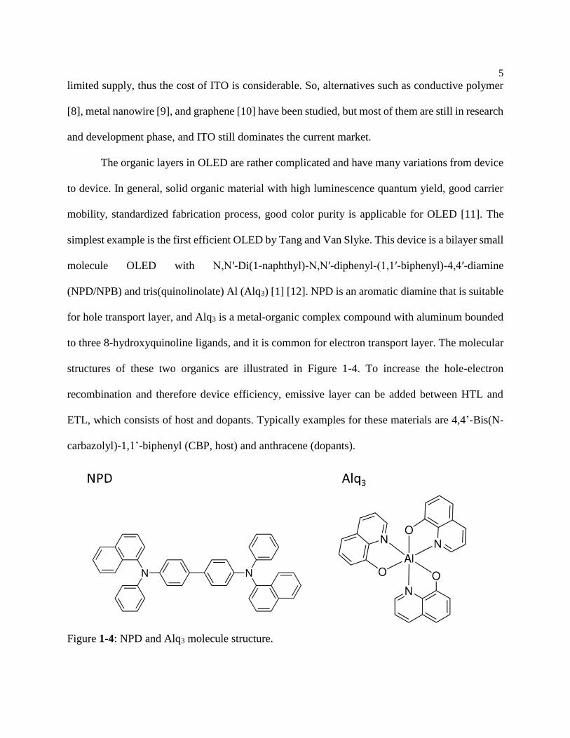
The organic layers in OLED are rather complicated and have many variations from device
to device. In general, solid organic material with high luminescence quantum yield, good carrier
mobility, standardized fabrication process, good color purity is applicable for OLED [11]. The
simplest example is the first efficient OLED by Tang and Van Slyke. This device is a bilayer small
molecule OLED with N,N′-Di(1-naphthyl)-N,N′-diphenyl-(1,1′-biphenyl)-4,4′-diamine
(NPD/NPB) and tris(quinolinolate) Al (Alq3) [1] [12]. NPD is an aromatic diamine that is suitable
for hole transport layer, and Alq3 is a metal-organic complex compound with aluminum bounded
to three 8-hydroxyquinoline ligands, and it is common for electron transport layer. The molecular
structures of these two organics are illustrated in Figure 1-4. To increase the hole-electron
recombination and therefore device efficiency, emissive layer can be added between HTL and
ETL, which consists of host and dopants. Typically examples for these materials are 4,4’-Bis(N-
carbazolyl)-1,1’-biphenyl (CBP, host) and anthracene (dopants).
Figure 1-4: NPD and Alq3 molecule structure.
6
It is very beneficial to apply an electron injection layer of LiF as it gives great enhancement
in the EL performance of the OLED [13] [14]. Even 0.5 nm is enough to cause band bending of
Alq3 ETL, therefore lowering the electron-injection barrier [13]. The cathode can be made of
highly conductive metal, and a low work function is preferred to minimize the electron injection
barrier. There are many candidates, but Al is the most used one due to its environmental stability
and low cost [15]. The encapsulation can be various, one way is to cover the cathode with a metal
thin film using polymer adhesion layer.
1.3 Fabrication process
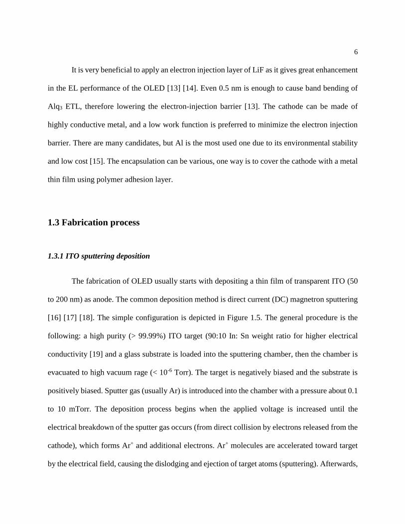
1.3.1 ITO sputtering deposition
The fabrication of OLED usually starts with depositing a thin film of transparent ITO (50
to 200 nm) as anode. The common deposition method is direct current (DC) magnetron sputtering
[16] [17] [18]. The simple configuration is depicted in Figure 1.5. The general procedure is the
following: a high purity (> 99.99%) ITO target (90:10 In: Sn weight ratio for higher electrical
conductivity [19] and a glass substrate is loaded into the sputtering chamber, then the chamber is
evacuated to high vacuum rage (< 10-6 Torr). The target is negatively biased and the substrate is
positively biased. Sputter gas (usually Ar) is introduced into the chamber with a pressure about 0.1
to 10 mTorr. The deposition process begins when the applied voltage is increased until the
electrical breakdown of the sputter gas occurs (from direct collision by electrons released from the
cathode), which forms Ar+ and additional electrons. Ar+ molecules are accelerated toward target
by the electrical field, causing the dislodging and ejection of target atoms (sputtering). Afterwards,

7
the sputtered target is deposited on the substrate, forming the ITO film. The deposition rate is
measured by a quartz crystal. Under an alternative current (AC) bias, the quartz crystal has a
resonance frequency dependent on the deposited thickness (mass), which can be used to calculate
the real time deposition rate. Noted that a tooling factor (the exact percentage of desired thickness
and accurately measured actual thickness after deposition) is needed, because different materials
have different mass to thickness ratio, and also there are other determinants like geometry of the
setup. The sputtering yield depends on the surface binding energy of the target, mass of the
sputtering gas ion, and the intensity of the electric field. Using magnetron sputtering source can
also increase the yield, as the magnetic field confines electrons near the target and results in more
collision with the sputtering gas.
After the ITO deposition and just before the following deposition of organic layers, an
additional surface treatment process can be made to minimize the defects on the ITO thus improve
the hole injection [20]. Chemical treatment with aquaregia [21], plasma treatment [22], and UV-
ozone treatment [20] can all increase the ITO work function, resulting in a reduced hole injection
barrier.

8
1.3.2 Vacuum thermal evaporation
For the deposition of organic layers, especially small molecule organic thin films, vacuum
thermal evaporation (VTE) [23] is the widely adapted by both academia for research purpose and
industry for device mass production. Figure 1-6 (a) is a basic schematic of a typical VTE system.
This deposition technique depends on electrically heating then evaporating the desired source
materials (usually in powder or pellet form) held in a metal boat or crucible (usually made of
tungsten, Figure 1-6 (b)), and the vapor will be deposited on the substrate. The whole process is
carried out in high vacuum (~ 10-7 Torr). The deposition rate is exponentially dependent on the
source temperature thus can be controlled by the current power, and it is monitored by a quartz
Figure 1-5: Schematic of the basic elements of a sputtering deposition system.

9
crystal. The real time monitored rate can also be in a feedback loop to adjust the current power so
that a stable deposition can be achieved. With multiple sources, co-evaporation for blends and
doped films is also available. The whole organic stack can be deposited sequentially [25].
For large area devices (mostly for commercial purpose), in-line source boats are used.
Figure 1-7 (c) is a simple illustration of this process [25]. In this case, the substrate is placed close
to a linear source boat of similar width, and organic film is deposited across the whole area as the
substrate moves over the source at certain speed. Different layers can be deposited by order when
the substrate travels from one source to another. Blends or doped film can be deposited by having
multiple linear sources next to each other, but slighted tilted so that the vapor flux from different
sources can overlapped when it reaches the substrate [25]. This method is very efficient to make
large OLED devices and has good thickness uniformity.
VTE is also used to deposit the LiF electron injection layer and the cathode metal, and it
generally requires higher electrical power for the cathode, as metals often have higher thermal
stability than organics. As a result, the substrate cooling is usually needed for many devices.

10
Figure 1-6: (a) Schematic of the basic elements of a VTE system. (b) a metal boat for source
material [24]. (c) in-line deposition simple illustration [25].
11
1.3.3 Encapsulation
The most convenient way to encapsulate OLED is to cover the cathode by a thin film with
extremely low water/oxygen permeability using appropriate adhesives. For laboratory practice,
one can use viscos optical adhesive to bond a piece of thin glass to the cathode side of the device,
then cure it by ultraviolet (UV) light. For industry manufacturers who need higher encapsulation
standard, epoxy resin-based adhesives are commonly used to attach a multilayer metal film to the
cathode. The whole process is conducted in glove box or other chemical inert environments.
1.4 Reliability issues of OLED
The two primary focuses in the current field of OLED are the light outcoupling and the
device reliability. The former helps to achieve even higher efficiency of OLED, giving more
brightness at the same operation voltage. The later helps to sustain the device performance and
extend the device lifetime. Here we will discuss the reliability issues of OLED lighting in three
major categories: extrinsic degradation, intrinsic degradation, and catastrophic failure.
1.4.1 Extrinsic degradation
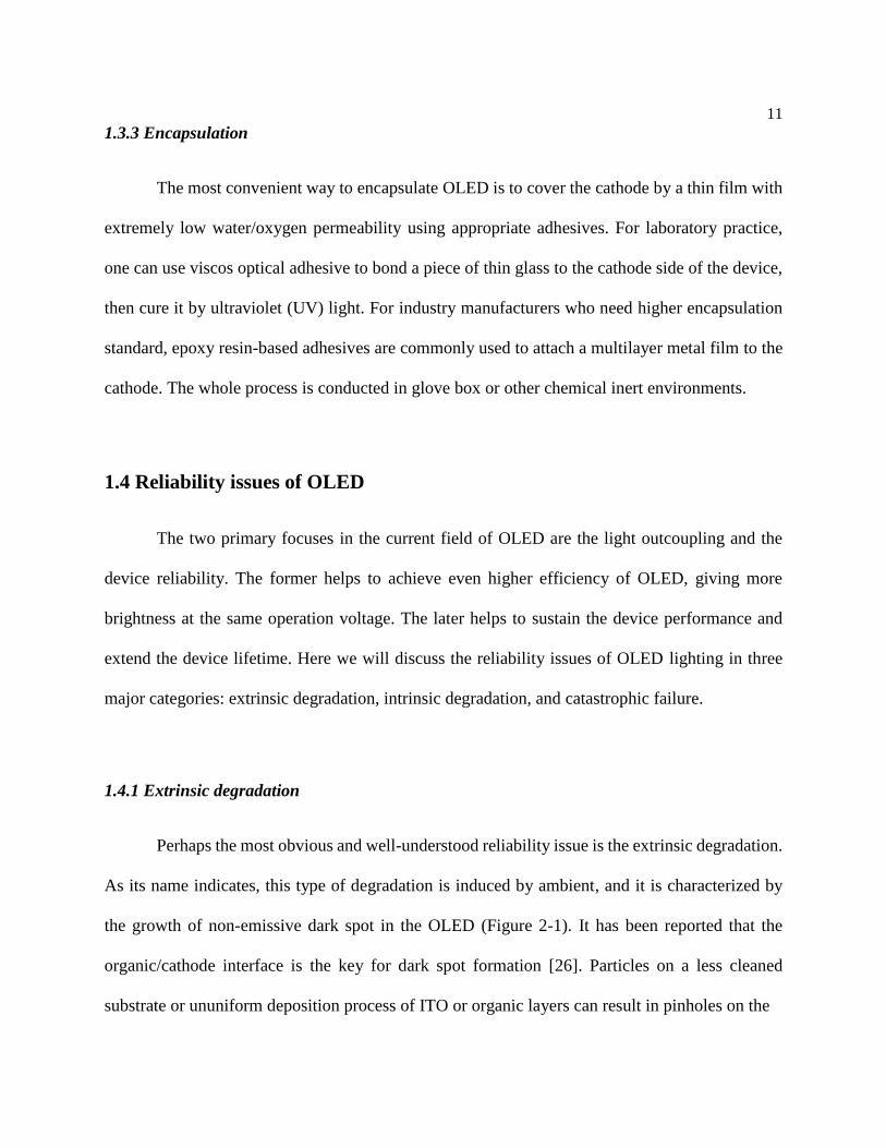
Perhaps the most obvious and well-understood reliability issue is the extrinsic degradation.
As its name indicates, this type of degradation is induced by ambient, and it is characterized by
the growth of non-emissive dark spot in the OLED (Figure 2-1). It has been reported that the
organic/cathode interface is the key for dark spot formation [26]. Particles on a less cleaned
substrate or ununiform deposition process of ITO or organic layers can result in pinholes on the
12
cathode due to the shadow effect, leaving open passages for ambient oxygen and water to reach
the organic layers, therefore, causing local oxidation of the organics [27]. This oxidation process
is directly affected by the pinhole size and the ambient moisture level, and it can be facilitated by
elevated temperature [26]. So, the growth of dark spot happens when the device is not operated
but can become more severe when the OLED is on due to the Joule heating.
The two most effective methods to suppress the extrinsic degradation are improving the
fabrication process and applying proper encapsulation. Ikeda et al. discovered a negative impact
on the device lifetime with increased process pressure (which is mostly related to the amount of
oxygen and moisture remaining in the process chamber) [28]. Purification of the materials and
substrate cleaning are also critical to the device performance and life time [29]. Encapsulation can
further reduce the dark spot formation and growth as it prevents ambient air and moisture to access
the organic layers [30]. Modern OLED manufacturers have highly standardized materials
purification, device fabrication process, and excellent encapsulation, so extrinsic degradation is
now less common in commercial OLED devices.
Figure 1-7: Optical microscope images of dark spots in an NPD/Alq3 bilayer OLED as a
result of extrinsic degradation (7 hours after device fabrication): (a) bright field (b)
electroluminescence [26].

13
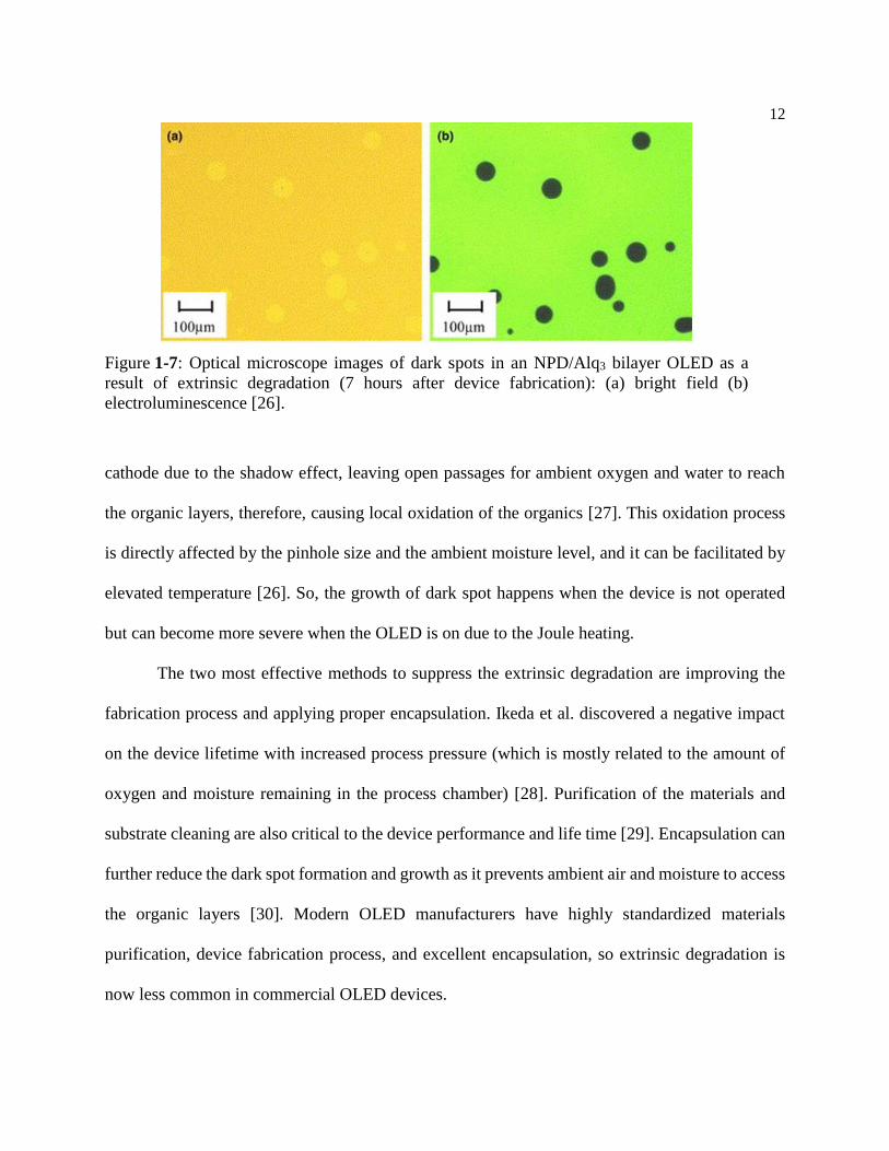
1.4.2 Intrinsic degradation
Intrinsic degradation is another distinct mode, and it exhibits as a gradual decrease in the
brightness of the OLED accompany with increase in driving voltage during continuous device
operation in a much longer time scale (~ days/weeks), but no obvious non-emissive area formation,
indicating an intrinsic loss of the OLED EL quantum efficiency [27] [31]. Unlike extrinsic
degradation, intrinsic degradation is eminently dependent on the materials used for the OLED. A
generally accepted explanation is that chemical conversion of some organic molecules occurs
gradually and leads to loss in luminance [31] [32]. Several models have been established. One
theory is the exciton induced degradation [33]. Excitons can contribute to defect formation, and
the defects can act as luminescent quenchers, nonradiative recombination centers, and deep charge
traps, all detrimental to the OLED EL efficiency [33]. Exciton-polaron (i.e. radical cation or anion)
annihilation is particularly important, as the experimental data of OLED luminance as a function
of operation time shows best agreement with this model prediction, suggesting it is the dominating
mechanism for the exciton induced degradation (Figure 1-9 (a)). Figure 1-9b is the configurational
diagram of the exciton-polaron annihilation: S0 is the excitonic ground state, S1/T1 is the first
singlet/triplet excited state, D0 is the polaronic ground state and Dn* is an excited state that lead to
the energy transfer and dissociation (state R) [33] [34]. The energy released during this process
can induced defects as it is enough to cause bond-breaking in the OLED chemicals. Intrinsic
degradation is somewhat unavoidable, but through careful materials selection and engineering, one
can remarkably decrease the luminance decay rate, so longer device overall lifetime can be
realized.
14
1.4.3 Catastrophic failure
Catastrophic failure is arguably the most pressing reliability issue for the OLED industry.
In this case, the whole device stops emitting light almost instantaneously due to local electrical
shorting that drains all the current from healthy region of the OLED [35]. Figure 1-10 (a) and (b)
show catastrophically failed OLED panels examples, and (c) shows the OLED luminance and
driving voltage plot as it begins to operate until it catastrophically failed (sudden drop in both
OLED light and voltage ((d) is the grey area in (c) zoomed-in). This type of failure is hardly
predictable, as it can occur at early stage of the device operation or later, and it can also not happen
at all before the device reaches LT70 lifetime, which is the time for EL efficiency to drop to 70%
of the initial value as a result of intrinsic degradation. While all OLED manufacturers take
mitigation steps to limit the damage of such failure, the physical origin remain poorly understood
and thus it is difficult to approach the problem fundamentally. Generally, it is believed that micro-
Figure 1-8: (a) Normalized OLED luminance vs operation time with initial brightness L0 = 1000,
2000, 3000, 4000 cd/m2. Fitting (solid line) is based on the exciton-polaron annihilation model.
(b) Configurational diagram of the exciton-polaron annihilation model, showing the energy
transfer from the exciton relaxation leads to the polaron excitation and dissociation. [33].

15
scale defects introduced during the OLED fabrication act as incipient shorts and evolve over a
period of operation time until shorting becomes substantial.
In this thesis, we will focus on catastrophic failure, as it is the major problem for our
studied OLED panels.
Figure 1-9: (a) Photograph of an OLED lighting fixture at OLED’s World Summit 2015. Red
circle indicates a catastrophically failed panel. (b) A catastrophically failed OLEDWorks Brite 1
device with dark residue in the organic layer. (c) OLED luminance (L) and driving voltage (VD)
versus time of continuous operation (NPD/Alq3 bilayer OLED). (d) Zoomed-in of (c) from 400
to 460 h. [35].

16
Chapter 2
Hypothesis and Main Method
The objective of this work is to develop a basic scientific understanding of catastrophic
shorts in OLED lighting panels: their origin and growth, and in the end, provide a path to mitigate
the catastrophic failure.
2.1 Nascent shorts
The lighting panels studied in this study are part of the Brite 1, Brite 2 and Bright Amber
product line manufactured by OLEDWorks, LLC. The Brite 1 and Brite 2 panels are multi-stack
white OLEDs with an active area of 102.4 mm × 102.4 mm constructed on glass substrates with a
traditional ITO anode and encapsulated with a multilayer thin film. Both panels have a rated
lifetime of 50,000 hrs at 3000 cd m-2 brightness and operate with luminous efficacies of 46 and 63
lm W-1, respectively. Brite Amber panels have an amber hue and also incorporate a multi-stack
OLED architecture. They are constructed on traditional ITO/glass substrates with an active area of
25 mm × 88 mm and are encapsulated with a metal can sealed by an edge bead of epoxy. Figure
2-1 (a) displays a photograph of a Brite Amber and Brite 1 panel in operation.
The working hypothesis is based on general understanding on catastrophic shorts:
microscale defects in OLED are nascent shorts, and they tend to grow over time and lastly become
catastrophic. Figure 2-1 (b) demonstrates a simplified circuit diagram: an OLED can be considered
as multiple light-emitting unit interconnecting each other. Each unit has a series resistance (Rs,
describing the ITO sheet resistance), and a shunt resistance (Rp, describing the OLED stack) in
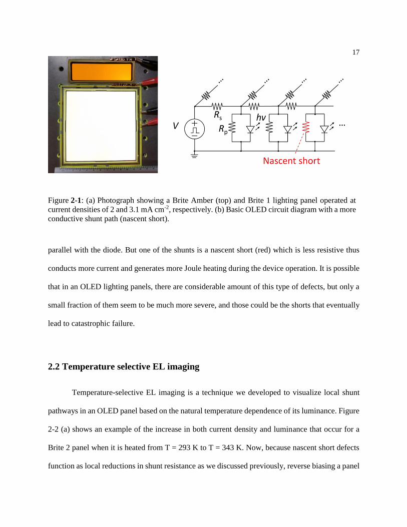
17
parallel with the diode. But one of the shunts is a nascent short (red) which is less resistive thus
conducts more current and generates more Joule heating during the device operation. It is possible
that in an OLED lighting panels, there are considerable amount of this type of defects, but only a
small fraction of them seem to be much more severe, and those could be the shorts that eventually
lead to catastrophic failure.
2.2 Temperature selective EL imaging
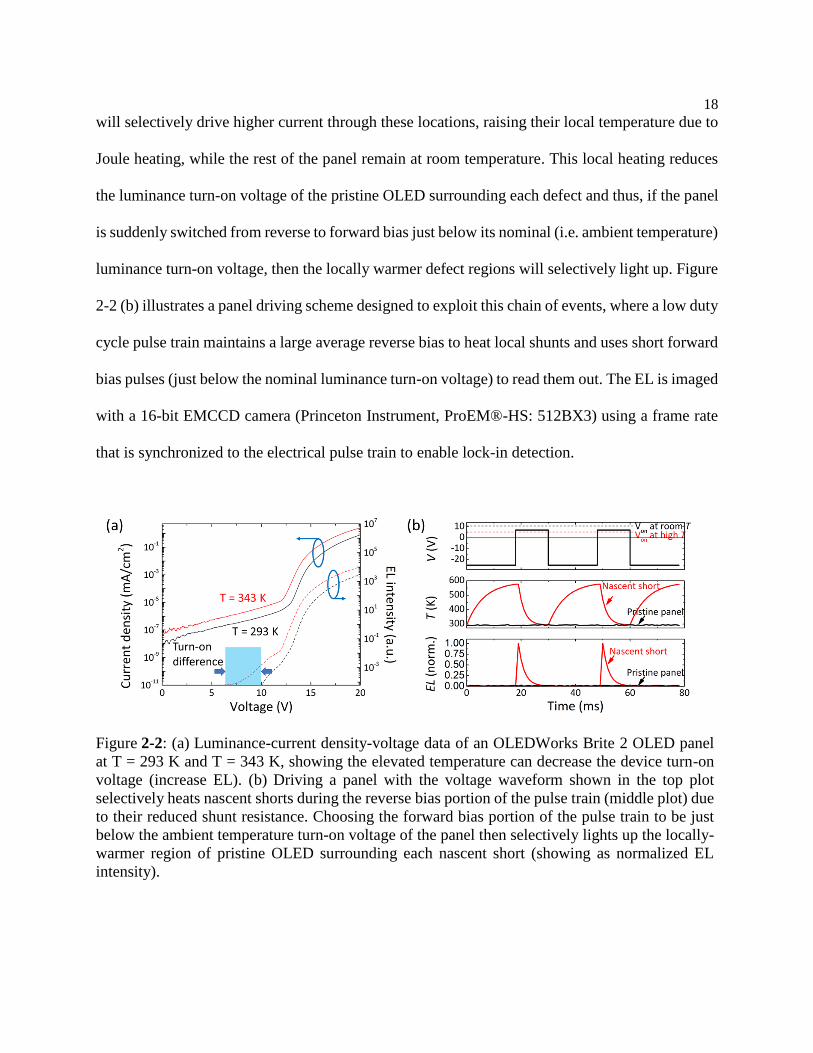
Temperature-selective EL imaging is a technique we developed to visualize local shunt
pathways in an OLED panel based on the natural temperature dependence of its luminance. Figure
2-2 (a) shows an example of the increase in both current density and luminance that occur for a
Brite 2 panel when it is heated from T = 293 K to T = 343 K. Now, because nascent short defects
function as local reductions in shunt resistance as we discussed previously, reverse biasing a panel
Figure 2-1: (a) Photograph showing a Brite Amber (top) and Brite 1 lighting panel operated at
current densities of 2 and 3.1 mA cm-2, respectively. (b) Basic OLED circuit diagram with a more
conductive shunt path (nascent short).
18
will selectively drive higher current through these locations, raising their local temperature due to
Joule heating, while the rest of the panel remain at room temperature. This local heating reduces
the luminance turn-on voltage of the pristine OLED surrounding each defect and thus, if the panel
is suddenly switched from reverse to forward bias just below its nominal (i.e. ambient temperature)
luminance turn-on voltage, then the locally warmer defect regions will selectively light up. Figure
2-2 (b) illustrates a panel driving scheme designed to exploit this chain of events, where a low duty
cycle pulse train maintains a large average reverse bias to heat local shunts and uses short forward
bias pulses (just below the nominal luminance turn-on voltage) to read them out. The EL is imaged
with a 16-bit EMCCD camera (Princeton Instrument, ProEM®-HS: 512BX3) using a frame rate
that is synchronized to the electrical pulse train to enable lock-in detection.
Figure 2-2: (a) Luminance-current density-voltage data of an OLEDWorks Brite 2 OLED panel
at T = 293 K and T = 343 K, showing the elevated temperature can decrease the device turn-on
voltage (increase EL). (b) Driving a panel with the voltage waveform shown in the top plot
selectively heats nascent shorts during the reverse bias portion of the pulse train (middle plot) due
to their reduced shunt resistance. Choosing the forward bias portion of the pulse train to be just
below the ambient temperature turn-on voltage of the panel then selectively lights up the locally-
warmer region of pristine OLED surrounding each nascent short (showing as normalized EL
intensity).
19
Chapter 3
Identifying, Characterizing, and Modelling Defects in OLED
3.1 Locating the defects
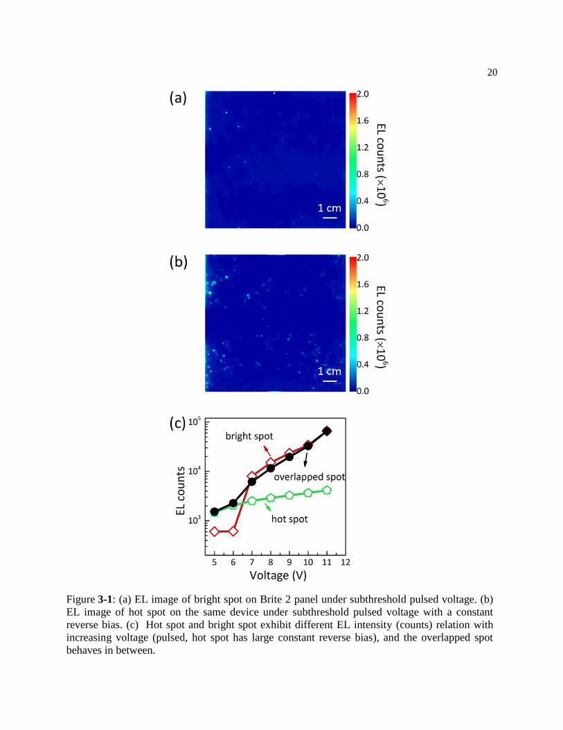
Using the temperature-selective EL imaging, we identify two major classes of defects,
naming them “bright spot” and “hot spot” based on their EL voltage driving condition. For bright
spot, the device is driven by a subthreshold pulsed voltage (~11 V for Brite 1/2 and 2/~5 V for
Brite Amber) with a pulse width of 17 ms and a period of 30 ms (normal threshold voltage is ~14
V for Brite 1 and 2, and ~6 V for Brite Amber), supplied by a source/measure unit (Keysight
B2912A). They can also be seen at same DC voltage. For hot spot, the device is driven by an even
lower forward pulse voltage (~8 V for Brite 1/2 and 2/~4 V for Brite Amber) while holding its
“off” state at a constant reverse bias (~-25 V for Brite 1/2 and 2/~-20V for Brite Amber) with same
duty cycle, and the camera electron-multiplying (EM) gain is set to be high to increase the light
sensitivity. A typical imaging result for Brite 2 panel is shown in Figure 3-1 (a) (bright spot) and
Figure 3-1 (b) (hot spot). The number of spots and their intensity (EL counts) can vary depend on
the driving condition, and two kinds of spots sometimes can overlap. Besides the driving condition,
bright spot and hot spot also have distinctive difference on the turn-on characteristics. As Figure
3-1 (c) showing their EL trend with increasing pulsed voltage, bright spot EL shows a diode-like
turn-on behavior at around 6 to 7 V (individual devices may vary), but hot spot EL tends to be a
gradual increase with voltage (in log scale), and when these two overlaps, the EL shares both
characteristics.
20
Figure 3-1: (a) EL image of bright spot on Brite 2 panel under subthreshold pulsed voltage. (b)
EL image of hot spot on the same device under subthreshold pulsed voltage with a constant
reverse bias. (c) Hot spot and bright spot exhibit different EL intensity (counts) relation with
increasing voltage (pulsed, hot spot has large constant reverse bias), and the overlapped spot
behaves in between.

21
3.2 Bright spot characterization
3.2.1 Optical microscopy
We first start with the optical microscopy, as it is the simplest method to see the physical
structure of bright spot. The Brite 1 panel is placed on the microscope stage and is driven by a
subthreshold DC bias. After locating the spot, different optical microscopy mode is used including
bright field, dark field, differential interference contrast (DIC), and EL. As Figure 3-2 shows,
bright field and dark field image reveal that bright spot is a physically visible particle with the size
around 10 µm (different bright spots vary from 5 to 20 µm). DIC image indicates the height
difference caused by this particle from the color contrast; and EL image taken at 14 V DC driving
voltage shows the light emission of the bright spot actually comes from the edges of the spot.
Figure 3-2: Various optical microscopy techniques on a bright spot on a Brite 1 panel. Images
taken through the glass substrate.

22
3.2.2 SEM and EDS
To acquire a more detailed look, the Brite 1 panel was dismantled by directly peeling off
the thin film encapsulation and the cathode attached to it, exposing the organic layers, then sputter
coated with 10 nm of iridium. The sample is examined by a scanning electron microscope (SEM)
with an energy dispersive X-ray spectroscopy (EDS) system built-in (FEI, Nova NanoSEM 630).
For the SEM image, we can see the small features on the spot, and the bright spot appears to be a
particle impacted and embedded on the surface of the substrate. The results from the EDS element
mapping clearly show increased In, Sn, and O signal at the bright spot area, suggesting it is ITO
agglomeration (Figure 3-3). Another set of samples are characterized with the same technique, but
we remove the organic layer by submerge the samples into acetone then isopropyl alcohol (IPA)
sonication for 5 minutes. Similar particles are observed at the bright spot region. We suspect this
is coming from an uncleaned ITO sputtering process that leaves uniformities on the ITO surface,
because Brite 2 panels show substantially less bright spots and their ITO anode is manufactured
with a new set of sputtering equipment. It is worth mentioning a few bright spots also show carbon
or silicon rich in the EDS analysis, but for most of these cases (>70%), they are ITO rich.
There is no definite explanation for their abnormal turn-on characteristics at this stage, but
we speculate two possible reasons: first, the local thickness variation of the organic layers caused
by these particles makes certain areas to have higher electric field, thus light emission could occur
even at subthreshold voltage; second, the whole device actually has slight light emission, and the
light is trapped inside the structure, but the geometry of the particle may scatter out the trapped
light, resulting in a bright spot. Since the bright spots show little connection with the catastrophic
failure in the accelerated aging test (will be discussed in later part of this thesis), less effort has
been focused on confirming these hypotheses.
23
3.3 Hot spot characterization
3.3.1 Magnified EL imaging
For hot spot, we start with similar optical microscopy method. However, hot spot seems to
be very dim (invisible to naked eye) and very small in size (extremely hard to locate under the
optical microscope). In this case, we use multiple mirrors and lenses to guide the light from the
microscope to the EMCCD camera to obtain the magnified EL image of hot spot. From Figure 3-
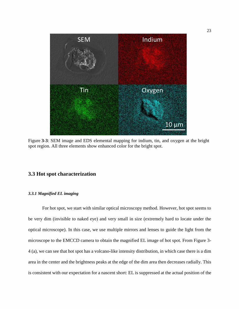
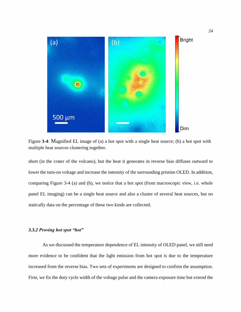
4 (a), we can see that hot spot has a volcano-like intensity distribution, in which case there is a dim
area in the center and the brightness peaks at the edge of the dim area then decreases radially. This
is consistent with our expectation for a nascent short: EL is suppressed at the actual position of the
Figure 3-3: SEM image and EDS elemental mapping for indium, tin, and oxygen at the bright
spot region. All three elements show enhanced color for the bright spot.
24
short (in the crater of the volcano), but the heat it generates in reverse bias diffuses outward to
lower the turn-on voltage and increase the intensity of the surrounding pristine OLED. In addition,
comparing Figure 3-4 (a) and (b), we notice that a hot spot (from macroscopic view, i.e. whole
panel EL imaging) can be a single heat source and also a cluster of several heat sources, but no
statically data on the percentage of these two kinds are collected.
3.3.2 Proving hot spot “hot”
As we discussed the temperature dependence of EL intensity of OLED panel, we still need
more evidence to be confident that the light emission from hot spot is due to the temperature
increased from the reverse bias. Two sets of experiments are designed to confirm the assumption.
First, we fix the duty cycle width of the voltage pulse and the camera exposure time but extend the
Figure 3-4: Magnified EL image of (a) a hot spot with a single heat source; (b) a hot spot with
multiple heat sources clustering together.

25
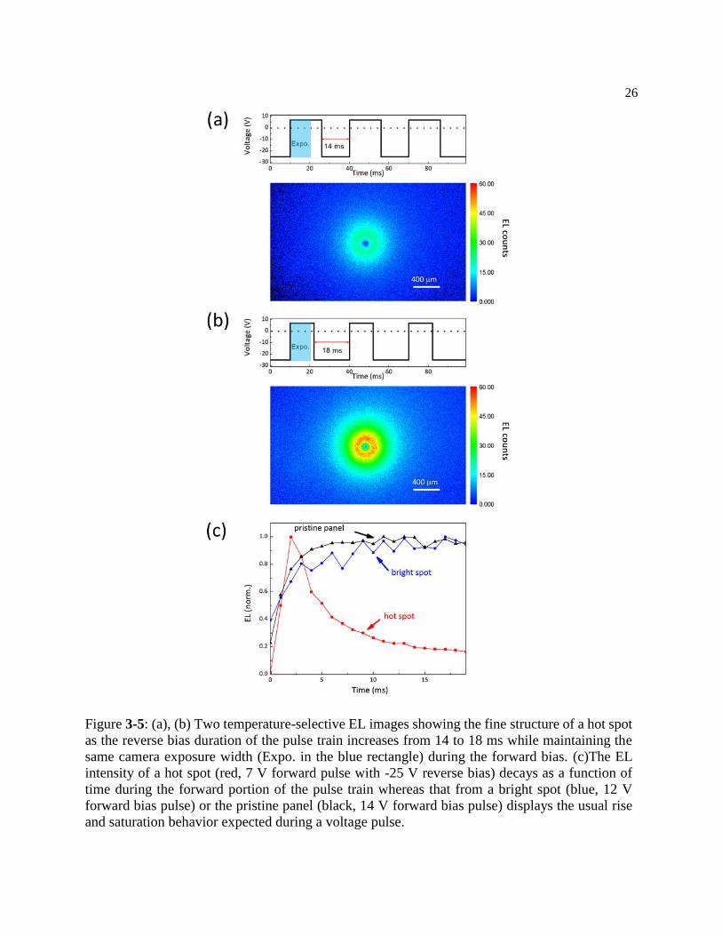
reverse bias duration, in other words, having a longer heating time for the hot spot, and its intensity
and size both show increase, indicating the dependence on temperature (Figure 3-5 (a) and (b)).
Similar effect on intensity and size is observed when the magnitude of the reverse bias is increased
(more power to raise the local temperature). Second, the intensity profile of both the hot spot,
bright spot, and the pristine panel during the forward bias pulse (20 s) are recorded with the
EMCCD camera. The result shows for the case of bright spot and pristine panel, the intensity
increases during the forward bias and reaches saturation, for hot spot, the intensity increases at the
very beginning of the pulse (possibly due to the signal delay of source/measure unit), then decays
as the time goes, which is expected as it reflects the dissipation of the heat accumulated during the
preceding reverse bias portion of the cycle (Ohmic heat generation is much smaller in forward bias
(7V) than in reverse bias (-25V) since it scales with the square of the voltage) (Figure 3-5 (c)).
26
Figure 3-5: (a), (b) Two temperature-selective EL images showing the fine structure of a hot spot
as the reverse bias duration of the pulse train increases from 14 to 18 ms while maintaining the
same camera exposure width (Expo. in the blue rectangle) during the forward bias. (c)The EL
intensity of a hot spot (red, 7 V forward pulse with -25 V reverse bias) decays as a function of
time during the forward portion of the pulse train whereas that from a bright spot (blue, 12 V
forward bias pulse) or the pristine panel (black, 14 V forward bias pulse) displays the usual rise
and saturation behavior expected during a voltage pulse.
27
3.3.3 Atomic force microscopy
Atomic force microscopy (AFM) is used to obtain an accurate physical structure of hot
spot. However, in this case, the Brite Amber OLED is used, because the encapsulation removing
process for Brite 1 and Brite 2 will remove the cathode as well, likely to ruin small features of the
hot spot. For Brite Amber panels, there is a space between encapsulation can and cathode, so hot
spot will be intact when removing the encapsulation. Figure 3-6 (a) and 3-6 (b) are the AFM image
and 2D line cuts of a hot spot on Brite Amber device through cathode. It is extremely small (< 3
µm) but has a relatively large height (~ 600 nm) comparing to the total thickness of the organic
layer (~ 200 nm). Noticeably there is a deep trench (more than 100 nm) along one side of the hot
spot, which is suspected to be a shadow effect from the device deposition and can possibly be the
heat source. Figure 3-6 (c) presents a basic explanation on this phenomenon: in OLEDWorks
device deposition system, the direction of each source is fixed, only the substrate moves. As the
result whenever there is a particle forming in any step of deposition, the following layers will have
vapor flux being partially blocked by the particle, causing one side to form shallow trench. When
the cathode is deposited, the metal that reaches into the trench is much closer to the anode ITO
compared to other area. Therefore, the electric field will be obviously higher, so as the local current
density, and that is the reason we believe the trenches are where the heat originates. Even though
bright spots are particles as well, their aspect ratio (average height to width) is not as extreme as
hot spots, and the shadow effect will not be as impactful as for hot spots (confirmed with optical
profilometry surface morphology measurement on bright spot).

28
3.3.4 Raman spectroscopy
For the chemical analysis, we used confocal Raman spectroscopy (HORIBA, LabRAM HR
Revolution) with a 785 nm laser excitation through the Brite Amber glass substrate and ITO, and
obtained the spectrum of the hot spot, the pristine panel, and certain organic layers in the stack as
reference. Figure 3-7 shows there are several intensity peaks of the hot spot match with the pristine
Figure 3-6: (a) AFM view of a hot spot (3×3 µm), showing its extremely small dimension. (b) 2D
line cuts of a hot spot which clearly reveals the trenches along the edge of the spot. (c) Simple
illustration to explain the difference of the hot spot and bright spot during the deposition.

29
panel, but at a much more intense level due to the higher thickness of the hot spot. Tracing those
peaks to the separate organic layers, and they match with particular peaks in the Raman spectrum
of electron transport mix (ET mix), emissive layer mix (EML mix) and Bathophenanthroline
(BPhen, common material in electron transport layer). Therefore, it is speculated that hot spots are
organic particulates is composed mainly of electron transport materials.
Figure 3-7: Raman spectrum of a hot spot, pristine panel, and several organic layers in the device.
The spectrum of hot spot shows increased peak intensity at several wavenumbers (dashed vertical
lines), indicating increased concentration of certain material(s) in the organic layer at the hot spot
location, which can include electron transport mix (ET mix), emissive layer mix (EML mix), and
bathophenanthroline (BPhen).
30
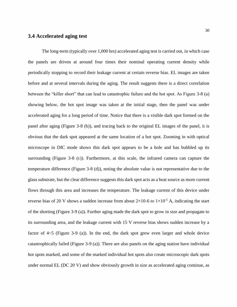
3.4 Accelerated aging test
The long-term (typically over 1,000 hrs) accelerated aging test is carried out, in which case
the panels are driven at around four times their nominal operating current density while
periodically stopping to record their leakage current at certain reverse bias. EL images are taken
before and at several intervals during the aging. The result suggests there is a direct correlation
between the “killer short” that can lead to catastrophic failure and the hot spot. As Figure 3-8 (a)
showing below, the hot spot image was taken at the initial stage, then the panel was under
accelerated aging for a long period of time. Notice that there is a visible dark spot formed on the
panel after aging (Figure 3-8 (b)), and tracing back to the original EL images of the panel, it is
obvious that the dark spot appeared at the same location of a hot spot. Zooming in with optical
microscope in DIC mode shows this dark spot appears to be a hole and has bubbled up its
surrounding (Figure 3-8 (c)). Furthermore, at this scale, the infrared camera can capture the
temperature difference (Figure 3-8 (d)), noting the absolute value is not representative due to the
glass substrate, but the clear difference suggests this dark spot acts as a heat source as more current
flows through this area and increases the temperature. The leakage current of this device under
reverse bias of 20 V shows a sudden increase from about 2×10⁻⁶ to 1×10⁻⁵ A, indicating the start
of the shorting (Figure 3-9 (a)). Further aging made the dark spot to grow in size and propagate to
its surrounding area, and the leakage current with 15 V reverse bias shows sudden increase by a
factor of 4~5 (Figure 3-9 (a)). In the end, the dark spot grew even larger and whole device
catastrophically failed (Figure 3-9 (a)). There are also panels on the aging station have individual
hot spots marked, and some of the marked individual hot spots also create microscopic dark spots
under normal EL (DC 20 V) and show obviously growth in size as accelerated aging continue, as
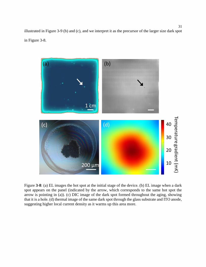
31
illustrated in Figure 3-9 (b) and (c), and we interpret it as the precursor of the larger size dark spot
in Figure 3-8.
Figure 3-8: (a) EL images the hot spot at the initial stage of the device. (b) EL image when a dark
spot appears on the panel (indicated by the arrow, which corresponds to the same hot spot the
arrow is pointing in (a)). (c) DIC image of the dark spot formed throughout the aging, showing
that it is a hole. (d) thermal image of the same dark spot through the glass substrate and ITO anode,
suggesting higher local current density as it warms up this area more.
32
Figure 3-9: (a) Leakage current measured during accelerated aging. The sudden drop (increase in
magnitude) after 3.5 days corresponds to the appearance the dark spot (DIC image). Continuing
aging, the magnitude of leakage current increased even though the measurement voltage was
decreased. After almost 10 days, another sudden drop occurred, corresponding to the growth of
the dark spot. At last, this dark spot propagated even larger and became a catastrophic short.
White dashed lines in optical images highlight the original dark spot (the scale bar is 200 µm).
(b) Optical microscopy image of one hot spot and the dark area developed around it at 20 V (Up: 196.6
hours aging. Down: 654.7 hrs aging). (c) Three different hot spots area growth through time of aging.

33
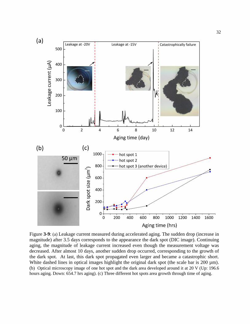
3.5 Heat transfer modelling for OLED
Due to the extreme dimension of the hot spot and the thick glass substrate, it is quite
impractical to have an accurate local temperature measurement. To have a basic understanding on
the temperature profile of the hot spot, a computational heat transfer model is necessary.
3.5.1 Experimental calibration of OLED temperature-luminance
Before building up the heat transfer model, a good approach to estimate the hot spot
temperature based on its magnified EL image is to correlate the device temperature and its
luminance via an experimental calibration. The OLED panel (Brite 1) is placed on a hot plat set to
be at a fixed temperature (from 293 to 363 K with an interval of 10 K), and its EL intensity at the
pristine area is recorded with the EMCCD camera at various DC voltage (within hot spot forward
pulsed bias range) after it reaches equilibrium. Since the metal encapsulation is highly thermally
conductive, it is fair to assume that the OLED internal temperature (organic layers) is close to the
hot plate temperature. We construct an empirical function to describe the OLED EL intensity (I,
counts in EMCCD image) with given temperature (T), operation voltage (V), and several constants
C1~4, including the Boltzmann constant (k) and fit it to the experimental data (Figure 3-10a):
𝐼 = exp[C1𝑉+C2
k𝑇+ C3𝑉 + C4] (3.1)
Assuming under hot spot driving mode, the pristine area far away from the center of the hot spot
is at room temperature (Tp = 293 K), we can calculate the hot spot temperature (Th) at each location
from its EL intensity by taking the natural log of the ratio between its intensity (Ih) and the pristine
area intensity (Ip) then solve for Th.

34
3.5.2 Building the heat transfer model
A 2D axisymmetric heat transfer model is built by COMSOL Multiphysics®. Figure 3-11
(a) shows the schematics and some important conditions for the model: the device structure
resembles the actual Brite 1 OLED, and there is a hot spot within the organic layer with a width
of 2 µm, and it is set to be a pulsed heat source (corresponding to the reverse bias). The top and
Figure 3-10: (a) Measured OLED EL counts from 7 V to 8.5 V DC bias at different temperatures
(scatter symbols) and the fitting based on the empirical function (dashed lines). (b) 1D line cut of
a hot spot EL counts and the calculated temperature; the dashed red line is the extrapolated
temperature based on the trend because the EL counts from the dim center is meaningless.
ln(𝐼ℎ
𝐼𝑝) = (C1𝑉 + C2)(
1
k𝑇ℎ−
1
k𝑇𝑝) (3.2)
Figure 3-10 (b) is the 1D line cut of the EL intensity of a hot spot and the corresponding calculated
temperature. Notice we can only extrapolate the temperature information in the hot spot center,
because it is a dim area and no reliable EL intensity data is available. From the plot we can see
the center can reach very high temperature (almost 700 K).
35
bottom boundary conditions are natural convection in room temperature air, and the side is open
boundary. Figure 3-11 (b) is example of the temperature profile within the device stack from the
simulation. The thermal parameters used in the simulation is shown in Table 3-1.
Figure 3-11: (a) Device structure and the related environmental conditions. (b) A sample image of
the temperature distribution in the simulated structure.
Table 3-1: Summary of the thermal parameters.
Materials Density (kg/m3) Heat capacity
(J/kgK)
Thermal
conductivity
(W/Km)
Reference
Al 3.9×10³ 900 238 COMSOL
built-in
Polymer resin 2×10³ 1000 0.2 [36] [37]
Organics 1.2×10³ 1700 0.2 [36] [37]
ITO 7.2×10³ 3400 8 [38]
Glass 2.21×10³ 730 1.4 COMSOL
built-in

36
3.5.3 Simulated temperature profile
Figure 3-12 plots the temperature of the organic layer at certain distance way from the
center of the hot spot as the heat pulse being sent into the spot. The temperature rises rapidly and
reaches almost equilibrium within one cycle (cycle width is 100 ms with 80 ms reverse bias and
20 ms forward pulse). The center of the hot spot can be extremely hot but it also drops significantly
as the heat propagates further within the organics. This result plus the previous calculation give us
an idea how hot these defects can possibly reach during the device operation, and at the very center,
it is certainly high enough to melt and vaporize the organics in the OLED.
Figure 3-12: Temperature of the organics at 0, 5, 25, 50, 100 µm away from the center of the hot
spot.

37
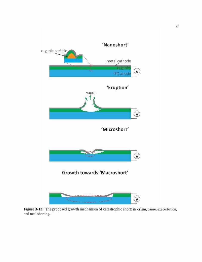
3.6 Proposed growth mechanism
Based on all the evidence and simulation, we established a hypothesis for the growth
mechanism (Figure 3-13). It starts with a sub-micron scale instability (hot spot) in the organic layer
which is more conductive due to the close distance between cathode and anode in the trench,
therefore has higher current density when the panel is in operation. The Joule heating makes this
area locally hotter and further increase the current density. Once the local temperature reaches a
certain level, the organic layers start to vaporize, which builds pressure and bubbles up the cathode,
causing delamination, and eventually ruptures the cathode like a volcano eruption. At this stage, a
visible dark spot has formed, but the panel can still be operational. This dark spot does not
necessarily lead to catastrophic failure if the fused organic “leftover” can cease the process, but in
other cases, the ruptured cathode may end up contacting the ITO anode directly, which
substantially increase the local current density thus the Joule heating, vaporizing more adjacent
organic materials, allowing more direct contact between cathode and anode, accelerating the
shorting process, and the growth of the dark spot. In the end of this process, the short is large
enough to be catastrophic and the device can no longer emit light.
38
Figure 3-13: The proposed growth mechanism of catastrophic short: its origin, cause, exacerbation,
and total shorting.

39
Chapter 4
Mitigation Strategies
One original goal of this study is to deliver a reliable way to predict the failure rate of an
OLED lighting panel based on its initial status such as hot spot number, distribution, intensity etc.,
so the reliability of an OLED can be determined and the product quality control can be improved.
However, the current failed devices from the accelerated aging (~ 8 in total) did not exhibit obvious
different characteristics compared to the still-healthy ones, so more statistics are required to check
if this goal is achievable. Meanwhile, since this failure is related to local heating caused by micro
shorting, the two main mitigation strategies will be eliminating the hot spots in during the device
fabrication or post fabrication process and applying anti-shorting layer to limit the level of
shorting.
4.1 Reducing hot spot
As it has been mentioned before, hot spots have trenches around them, which could cause
local high electric field/electrical conductivity due to the reduced organics thickness, making hot
spots to have higher temperature during operation. Since this can be a result of particle shadowing,
one possible solution is to introduce multi-angle deposition or substrate rotation. If the organic
vapor is deposited on the substrate from two or more sources, even though there can be particles,
the thickness uniformity will be much better, as the shadowing can be compensated by the vapor
from the opposite direction. Similar principle applies to substrate rotation. To test this method,
40
4.2 Anti-shorting layer
The alternative approach than solving the issue from its origin is to keep the shorts from
becoming catastrophic, giving that micro-scale shorts are allowed as long as they are not obvious
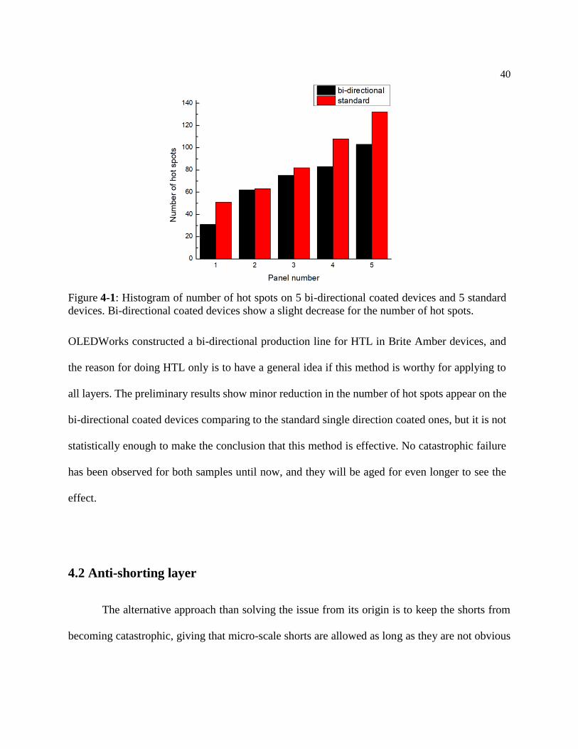
Figure 4-1: Histogram of number of hot spots on 5 bi-directional coated devices and 5 standard
devices. Bi-directional coated devices show a slight decrease for the number of hot spots.
OLEDWorks constructed a bi-directional production line for HTL in Brite Amber devices, and
the reason for doing HTL only is to have a general idea if this method is worthy for applying to
all layers. The preliminary results show minor reduction in the number of hot spots appear on the
bi-directional coated devices comparing to the standard single direction coated ones, but it is not
statistically enough to make the conclusion that this method is effective. No catastrophic failure
has been observed for both samples until now, and they will be aged for even longer to see the
effect.

41
by human eye. The most direct way is to use an insulating short reduction layer to limit the amount
of current flowing.
4.2.1 Insulating oxide layer
This method involves depositing an ultra-thin layer (< 8 nm) of insulating oxide on top of
the ITO anode, so that sufficient current can still tunnel through for normal device operation. When
the organics vaporize and the cathode delaminate and erupt, the resistance of the oxide layer can
prevent a large mount of current flowing at this point, then keep the rest of the OLED safe from
shorting. The drawbacks are also quite obvious, as adding an additional insulating layer, though
very thin, will rise up the operation voltage and lower the brightness of the OLED. Alumina
(Al2O3) has been tested on Brite Amber devices by atomic layer deposition (ALD), which has high
precision in thickness control and excellent surface uniformity. Samples with various thicknesses
are fabricated and currently under accelerated aging test to see if this method will useful. No
definite conclusion can be drawn at this point.
4.2.2 Teflon “fuse” layer
J. Price et al. has demonstrated improved thermal stability and, surprisingly, carrier
transport ability for NPD by co-evaporate polytetrafluoroethylene (PTFE, best known as Teflon)
[40]. They proved that during the evaporation, Teflon amorphous fluoroplastics (TAF) polymer
chain breaks into little fragments and deposits on the substrate in mixture with the NPD molecule,
then, TAF re-polymerizes and forms a network with nanoporous filled by NPD (Figure 4-2a). As
TAF is a thermoplastic material with a high melting point of 327 ℃ [39], this network structure
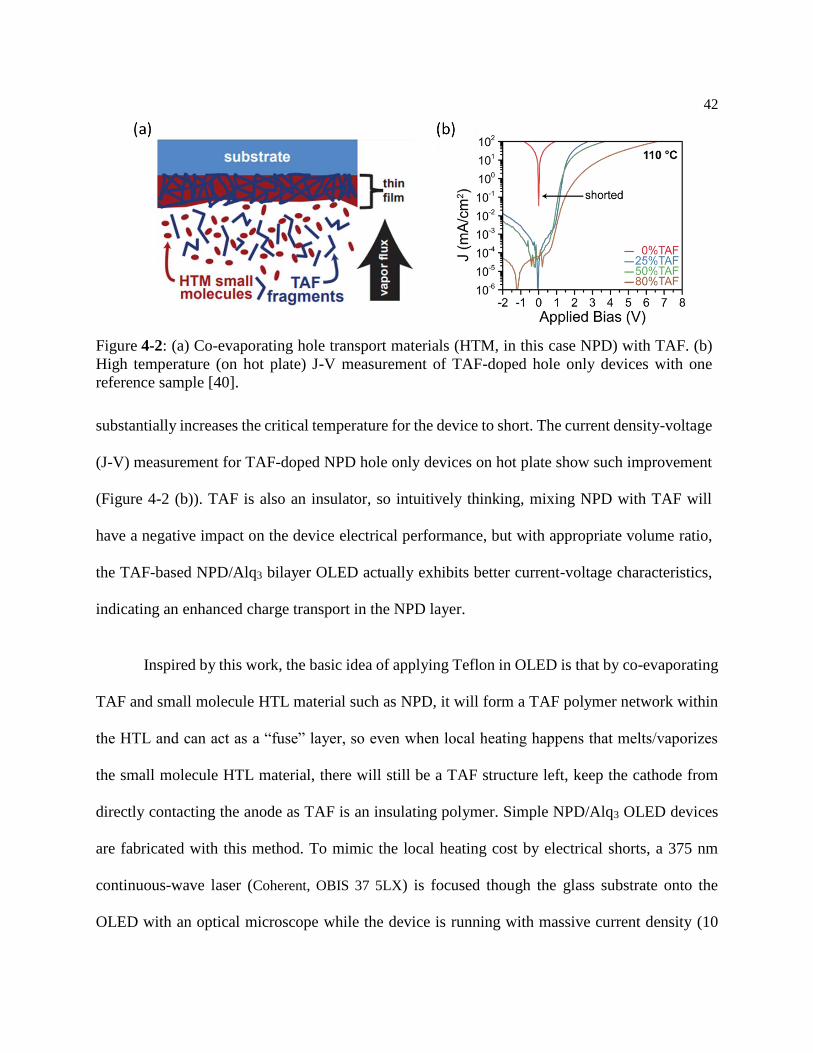
42
Inspired by this work, the basic idea of applying Teflon in OLED is that by co-evaporating
TAF and small molecule HTL material such as NPD, it will form a TAF polymer network within
the HTL and can act as a “fuse” layer, so even when local heating happens that melts/vaporizes
the small molecule HTL material, there will still be a TAF structure left, keep the cathode from
directly contacting the anode as TAF is an insulating polymer. Simple NPD/Alq3 OLED devices
are fabricated with this method. To mimic the local heating cost by electrical shorts, a 375 nm
continuous-wave laser (Coherent, OBIS 37 5LX) is focused though the glass substrate onto the
OLED with an optical microscope while the device is running with massive current density (10
Figure 4-2: (a) Co-evaporating hole transport materials (HTM, in this case NPD) with TAF. (b)
High temperature (on hot plate) J-V measurement of TAF-doped hole only devices with one
reference sample [40].
substantially increases the critical temperature for the device to short. The current density-voltage
(J-V) measurement for TAF-doped NPD hole only devices on hot plate show such improvement
(Figure 4-2 (b)). TAF is also an insulator, so intuitively thinking, mixing NPD with TAF will
have a negative impact on the device electrical performance, but with appropriate volume ratio,
the TAF-based NPD/Alq3 bilayer OLED actually exhibits better current-voltage characteristics,
indicating an enhanced charge transport in the NPD layer.
43
times the normal level). The Teflon-based devices have much lower shorting rate (1 out of 10
devices) while all the reference samples are shorted at the same condition. This promising result
give OLEDWorks confidence to test it with amber OLED that has more complicated structure
(multi-stack) but starts with an NPD-TAF HTL Again, the TAF-based OLEDs show considerable
improvement in device performance such as luminance efficacy, external quantum efficiency
(EQE), and turn-on voltage. But the laser shorting technique is inclusive as all devices including
reference do not short or fail from different mechanism other than the catastrophic short induced
by local heating. So, more devices have been fabricated for the standard accelerated aging test,
where the failure is closer to the natural catastrophic short. The experiment is still in progress.
44
Chapter 5
Summary and Outlook
In this thesis, we generally discussed the background of OLED: the typical OLED
applications like display and lighting, the working principle of OLED, a few simple materials used
in OLED, how to fabricate an OLED, and the reliability challenge of OLED. The focus of this
work is the catastrophic failure in commercial OLED lighting panel, and our hypothesis is that
nascent shorts caused by microscale defects in OLED initiate the failure and grow over time to
become catastrophic. We developed a temperature selective EL imaging method based on the
dependence of OLED luminance on device temperature, and this method can effectively locate the
nascent shorts at the early stage of the panel lifetime. Two general classes of defects are identified
as bright spot and hot spot. These defects are investigated via various characterization techniques
including optical microscopy, SEM/EDS, AFM, and Raman spectroscopy, and large number of
devices are tested on accelerated aging station. We found bright spots tend to associate with ITO
agglomerations and are largely benign, while hot spots tend to associate with microscale organic
semiconductor particulates, mostly electron and constitute local shunts that can grow into
catastrophic shorts. Using COMSOL heat transfer model, we predict that the center of the hot spot
can reach high enough temperature that can vaporize the organics. With all the information, we
propose a “volcano eruption” model for the catastrophic failure in OLED: the failure starts from a
hot spot, and during the device operation, the local heating becomes more severe and vaporize the
organic layer, causing the delamination and then rupture of the cathode; the cathode now can
directly touch the anode, causing more Joule heating and accelerate the failure process until it
becomes catastrophic. To mitigate this type of degradation, we introduce a few methods including

45
reducing the number of hot spots by multi-angle device deposition and deploying an anti-shorting
layer in the OLED.
As we now understand the origin and the growth of the catastrophic failure, and proposed
several feasible mitigation strategies, OLED lighting panel manufactures can benefit from this
work in terms of improving their product reliability from the fabrication as well as exploring
methods to reduce catastrophic failure.
46
Bibliography
[1] C. W. Tang and S. A. Vanslyke, “Organic electroluminescent diodes,” Appl. Phys. Lett.,
vol. 51, no. 12, pp. 913–915, 1987.
[2] Samsung. Galaxy. https://www.samsung.com/us/mobile/galaxy/ (Aug. 2018).
[3] Apple. iPhone. https://www.apple.com/iphone/ (Aug. 2018).
[4] Huawei. P20 Pro. https://consumer.huawei.com/cn/phones/p20-pro/ (Aug. 2018).
[5] LG Business Solution. OLED. https://www.lg.com/global/business/information-
display/technology-solution/oled (Aug. 2018).
[6] LG. Luflex OLED. https://www.lgoledlight.com/about-luflex/?ckattempt=1 (Aug. 2018).
[7] M. A. Baldo et al., “Highly efficient phosphorescent emission from organic
electroluminescent devices,” Nature, vol. 395, no. 6698, pp. 151–154, 1998.
[8] B. K. Fehse, K. Walzer, K. Leo, W. Lövenich, and A. Elschner, “Highly Conductive
Polymer Anodes as Replacements for Inorganic Materials in High-Efficiency Organic
Light-Emitting Diodes ,” Adv. Mater., vol. 19, pp. 441–444, 2007.
[9] J. Lee, S. T. Connor, Y. Cui, and P. Peumans, “Solution-Processed Metal Nanowire Mesh
Transparent Electrodes,” Nano Lett., vol. 8, pp. 689–692, 2008.
[10] J. Wu et al., “Organic solar cells with solution-processed graphene transparent electrodes
Organic solar cells with solution-processed graphene,” Appl. Phys. Lett., vol. 92, no.
263302, 2009.
[11] B. Geffroy, P. le Roy, and C. Prat, “Organic light-emitting diode (OLED) technology:
Materials, devices and display technologies,” Polym. Int., vol. 55, no. 6, pp. 572–582,
2006.
[12] S. A. Van Slyke, C. H. Chen, and C. W. Tang, “Organic electroluminescent devices with
improved stability,” Appl. Phys. Lett., vol. 69, pp. 2160–2162, 1996.
47
[13] L. S. Hung, C. W. Tang, and M. G. Mason, “Enhanced electron injection in organic
electroluminescence devices using an Al / LiF electrode,” Appl. Phys. Lett., vol. 70, pp.
152–154, 1997.
[14] X. J. Wang et al., “Enhancement of electron injection in organic light-emitting devices
using an Ag / LiF cathode,” J. Appl. Phys., vol. 95, no.7, pp. 3828-3830, 2004.
[15] N. Erickson. PhD Dissertation, “On the Properties and Design of Organic Light-Emitting
Devices,” The Univeristy of Minnesota. January, 2014.
[16] R. Latz et al., “High Conducting Large Area Indium Tin Oxide Electrodes for Displays
Prepared by DC Magnetron Sputtering,” J. Appl. Phys., vol. 30, pp. L149-L151, 1991.
[17] W. Deng, T. Ohgi, H. Nejo, and D. Fujita, “Development of conductive transparent
indium tin oxide ( ITO ) thin films deposited by direct current ( DC ) magnetron sputtering
for photon-STM applications,” Appl. Phys. A, vol. 72, pp. 595–601, 2001.
[18] O. Tuna, Y. Selamet, G. Aygun, and L. Ozyuzer, “High quality ITO thin films grown by
dc and RF sputtering without oxygen,” J. Phys. D: App. Phys., vol. 43, no. 055402, 2010.
[19] F. O. Adurodija et al., “Influence of substrate temperature on the properties of indium
oxide thin films,”J. Vac. Sci. Technol. A, vol. 18, pp. 814–818, 2000.
[20] B. Kim, D. Kim, Y. Jang, N. Lee, O. Kwon, and Y. Kwon, “UV-Ozone Surface Treatment
of Indium-Tin-Oxide in Organic Light Emitting Diodes,” J. Korean Phys. Soc., vol. 50,
no. 6, pp. 1858–1861, 2007.
[21] F. Li et al., “Effects of aquaregia treatment of indium – tin – oxide substrates on the
behavior of double layered organic light-emitting diodes,” Appl. Phys. Lett., vol. 70, pp.
2741–2743, 1997.
[22] J. S. Kim, F. Cacialli, A. Cola, G. Gigli, and R. Cingolani, “Increase of charge carriers
density and reduction of Hall mobilities in oxygen-plasma treated indium – tin – oxide
anodes,” Appl. Phys. Lett., vol. 75, pp. 19-21, 1999
[23] S. R. Forrest, “Ultrathin Organic Films Grown by Organic Molecular Beam Deposition
and Related Techniques,” Chem. Rev. vol 97, pp. 1793-1896, 1997.

48
[24] Testbourne Ltd. Baffled Box Sources for SiO, ZnS. http://www.testbourne.com/vacuum-
evaporation-sources-baffled-box-sources-for-sio-zns. (Aug. 2018).
[25] S. Forrest. Unpublished organic optoelectronics book. EE597 class material. 2017
[26] Y. Liew et al. "Effect of organic layer coombination on dark spot formation in organic
light emitting devices," Chem. Phys. Lett. vol 394, pp 275-279, 2004.
[27] J. Mcelvain et al., “Formation and growth of black spots in organic light-emitting diodes
Formation and growth of black spots in organic light-emitting diodes,” J. Appl. Phys., vol.
80, pp. 6002-6007, 1996.
[28] T. Ikeda, H. Murata, Y. Kinoshita, and J. Shike, “Enhanced stability of organic light-
emitting devices fabricated under ultra-high vacuum condition,” Chem. Phys. Lett., vol.
426, pp. 111–114, 2006.
[29] S. Scholz, D. Kondakov, and K. Leo, “Degradation Mechanisms and Reactions in Organic
Light-Emitting Devices,” Chem. Rev., vol. 115, pp.8449-8503, 2015.
[30] P. E. Burrows, V. Bulovic, S. R. Forrest, L. S. Sapochak, D. M. McCarty, and M. E.
Thompson, “Reliability and degradation of organic light emitting devices,” Appl. Phys.
Lett., vol. 65, no. 23, pp. 2922–2924, 1994.
[31] H. Aziz and Z. D. Popovic, “Degradation phenomena in small-molecule organic light-
emitting devices,” Chem. Mater., vol. 16, no. 23, pp. 4522–4532, 2004.
[32] S. Schmidbauer, A. Hohenleutner, and B. König, “Chemical degradation in organic light-
emitting devices: Mechanisms and implications for the design of new materials,” Adv.
Mater., vol. 25, no. 15, pp. 2114–2129, 2013.
[33] N. C. Giebink et al., “Intrinsic luminance loss in phosphorescent small-molecule organic
light emitting devices due to bimolecular annihilation reactions,” J. Appl. Phys., vol. 103,
no. 4, 2008.
[34] S. R. Forrest, “Excitons and the lifetime of organic semiconductor devices,” Phil. Trans.
R. Soc. A., vol. 273, 2015.
[35] P. R. F. Rocha et al., “Sudden death of organic light-emitting diodes,” Org. Electron., vol.
49
20, pp. 89–96, 2015.
[36] X. Qi, and S. R. Forrest, “Thermal analysis of high intensity organic light-emitting diodes
based on a transmission matrix approach,” J. Appl. Phys., vol. 110, no. 214516, 2011.
[37] H. Lee, “Rapid measurement of thermal conductivity of polymer films,” Rev. Sci. Instrum.
vol. 53, pp. 884-887, 1982.
[38] W. H. Tanttila. "Anomalous Thermal Properties of Glasses," Phys. Rev. Lett., vol. 39, no.
9, pp. 8–11, 1977.
[39] Chemours. Fluoroplastic Comparison - Typical Properties.
https://www.chemours.com/Teflon_Industrial/en_US/tech_info/techinfo_compare.html
(Aug. 2018)
[40] J. Price. PhD Dissertation, “High Efficiency Planar Solar Concentrators and Novel
Structures for Orgnics Light Emitting Diodes,” The Pennsylvanis State Univeristy. May,
2018.


