Embed Size (px)
Citation preview

1SZZA036C–December 2002–Revised June 2016Submit Documentation Feedback
Copyright © 2002–2016, Texas Instruments Incorporated
Understanding and Interpreting Standard-Logic Data Sheets
Application ReportSZZA036C–December 2002–Revised June 2016
Understanding and InterpretingStandard-Logic Data Sheets
Stephen M.Nolan, Jose M. Soltero, Shreyas Rao
ABSTRACTTexas Instruments (TI) standard-logic product data sheets include descriptions of functionality andelectrical specifications for the devices. Each specification includes acronyms, numerical limits, and testconditions that may be foreign to the user. The proper understanding and interpretation of the direct, andsometimes implied, meanings of these specifications are essential to correct product selection andassociated circuit design. This application report explains each data sheet parameter in detail, how itaffects the device, and how it impacts the application. This will enable component and system-designengineers to derive the maximum benefit from TI logic devices.
Contents1 Application Note Outline .................................................................................................... 22 Introduction ................................................................................................................... 23 Top-Level Look at the TI Logic Data Sheet .............................................................................. 3
3.1 Device Summary.................................................................................................... 43.2 Pin Configuration and Functions.................................................................................. 63.3 Absolute Maximum Ratings ....................................................................................... 63.4 ESD Ratings......................................................................................................... 73.5 Recommended Operating Conditions............................................................................ 83.6 Electrical Characteristics........................................................................................... 83.7 Live-Insertion Specifications....................................................................................... 93.8 Timing Requirements ............................................................................................. 103.9 Switching Characteristics......................................................................................... 103.10 Noise Characteristics ............................................................................................. 113.11 Operating Characteristics ........................................................................................ 113.12 Parameter Measurement Information........................................................................... 12
4 Dissecting the TI Logic Data Sheet ...................................................................................... 144.1 Summary Device Description .................................................................................... 144.2 Revision History ................................................................................................... 244.3 Pin Configuration And Functions ................................................................................ 244.4 Absolute Maximum Ratings ...................................................................................... 244.5 Recommended Operating Conditions .......................................................................... 274.6 Electrical Characteristics ......................................................................................... 354.7 Live-Insertion Specifications ..................................................................................... 474.8 Timing Requirements ............................................................................................. 474.9 Switching Characteristics......................................................................................... 504.10 Noise Characteristics ............................................................................................. 544.11 Operating Characteristics ........................................................................................ 554.12 Parameter Measurement Information........................................................................... 56
5 Logic Compatibility ......................................................................................................... 566 Detailed Description........................................................................................................ 577 Application and Implementation .......................................................................................... 578 Power Supply Recommendations........................................................................................ 589 Layout........................................................................................................................ 58

Application Note Outline www.ti.com
2 SZZA036C–December 2002–Revised June 2016Submit Documentation Feedback
Copyright © 2002–2016, Texas Instruments Incorporated
Understanding and Interpreting Standard-Logic Data Sheets
10 Conclusion .................................................................................................................. 5811 Acknowledgments .......................................................................................................... 5812 References .................................................................................................................. 58
1 Application Note OutlineThis application report is organized into five main sections:1. Introduction2. Top-Level Look at the TI Logic Data Sheet. Overall layout and component parts of a data sheet are
explained.3. Dissecting the TI Logic Data Sheet. JEDEC definition, the TI definition, an explanation, and, where
possible, helpful hints are presented for each specification term commonly found in TI logic datasheets.
4. Logic Compatibility. Information in TI logic data sheets for determining the interface compatibilitybetween different logic families is explained.
5. End matter, including the Conclusion, Acknowledgments, and References sections.
2 IntroductionThis application report is a synopsis of the information available from a typical TI data sheet with thepurpose of assisting component and system-design engineers in selecting Texas Instruments (TI)standard-logic products. Information includes a brief description of terms, definitions, and testingprocedures currently used for commercial, automotive and military specifications. Symbols, terms, anddefinitions generally are in accordance with those currently agreed upon by the JEDEC Solid StateTechnology Association for use in the USA and by the International Electrotechnical Commission (IEC) forinternational use.
www.ti.com Top-Level Look at the TI Logic Data Sheet
3SZZA036C–December 2002–Revised June 2016Submit Documentation Feedback
Copyright © 2002–2016, Texas Instruments Incorporated
Understanding and Interpreting Standard-Logic Data Sheets
3 Top-Level Look at the TI Logic Data SheetThe TI logic data sheet presents pertinent technical information for a particular device and is organized forquick access. This application report dissects a typical TI logic data sheet and describes the organizationof all data sheets.
Typically, there are ten sections in TI-logic data sheets:1. Front Page
(a) Features(b) Applications(c) Description(d) Device Information Table(e) Front-Page Graphic(s)
2. Table of Contents3. Revision History4. Pin Configuration and Functions5. Specifications
(a) Absolute Maximum Ratings(b) ESD Ratings(c) Recommended Operating Conditions(d) Thermal Information(e) Electrical Characteristics(f) Timing Requirements(g) Switching Characteristics(h) Typical Characteristics
6. Parameter Measurement Information7. Detailed Description
(a) Overview(b) Functional Block Diagram(c) Feature Description(d) Device Functional Modes
8. Application and Implementation(a) Application Information(b) Typical Application(c) Design Requirements(d) Detailed Design Procedure(e) Application Curves
9. Power Supply Recommendations10. Layout
(a) Layout Guidelines(b) Layout Example
11. Device and Documentation Support12. Mechanical, Packaging, and Ordering Information
Top-Level Look at the TI Logic Data Sheet www.ti.com
4 SZZA036C–December 2002–Revised June 2016Submit Documentation Feedback
Copyright © 2002–2016, Texas Instruments Incorporated
Understanding and Interpreting Standard-Logic Data Sheets
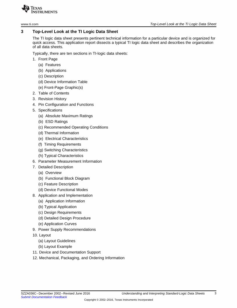
3.1 Device SummaryThe first page of a data sheet contains all of the general information about a device (see Figure 1). Thisinformation includes:1. Title, literature number, and dates of origination and revision, as applicable. Also, the top navigation
contains hyperlinks leading directly to Product Folder, Sample & Buy, Technical Documents (related tothe device), Tools & Software, and Support & Community.
Figure 1. Example of Device Summary
2. The Features section identifies the main features and benefits of the device. This section includesfeatures in a bulleted form. Figure 2 shows an example of the bulleted features.
Figure 2. Feature Bullets
3. The Applications section for the device identifies the application scenarios for the device. Figure 3shows an example of typical applications.
Figure 3. Typical Applications
4 Revision History
Changes from Revision X (March 2014 to Revision Y
Device Information(1)
DEVICE NAME PACKAGE BODY SIZE
SOT-23 (5) 2.9mm × 1.6mm
SC70 (5) 2.0mm × 1.25mm
SON (6) 1.45mm × 1.0mm
SON (6) 1.0mm × 1.0mm
(1) For all available packages, see the orderable addendum atthe end of the datasheet.
SN74LVC1G08 X2SON (4) 0.8mm × 0.8mm
www.ti.com Top-Level Look at the TI Logic Data Sheet
5SZZA036C–December 2002–Revised June 2016Submit Documentation Feedback
Copyright © 2002–2016, Texas Instruments Incorporated
Understanding and Interpreting Standard-Logic Data Sheets
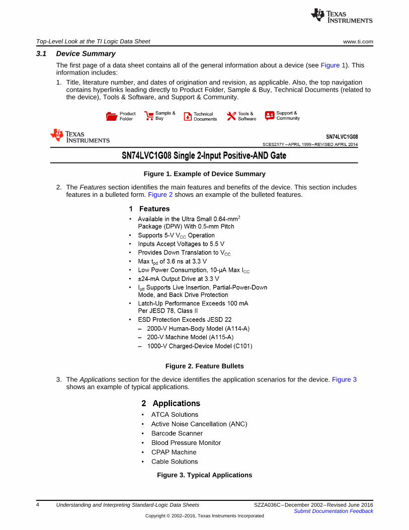
4. The Description section provides a brief description of the device and its functionality
Figure 4. Brief Description of Device
5. Figure 5 shows a logic diagram. The device information defines the nominal size of the device in eachof the available packages.
Figure 5. Device Information
6. Product-development stage note at the bottom of the data sheet7. Table of contents to list the contents and the link to the page numbers alongside it.8. Revision history for the device mentioning the changes to the data sheet with the dates.
Figure 6. Revision History
Top-Level Look at the TI Logic Data Sheet www.ti.com
6 SZZA036C–December 2002–Revised June 2016Submit Documentation Feedback
Copyright © 2002–2016, Texas Instruments Incorporated
Understanding and Interpreting Standard-Logic Data Sheets
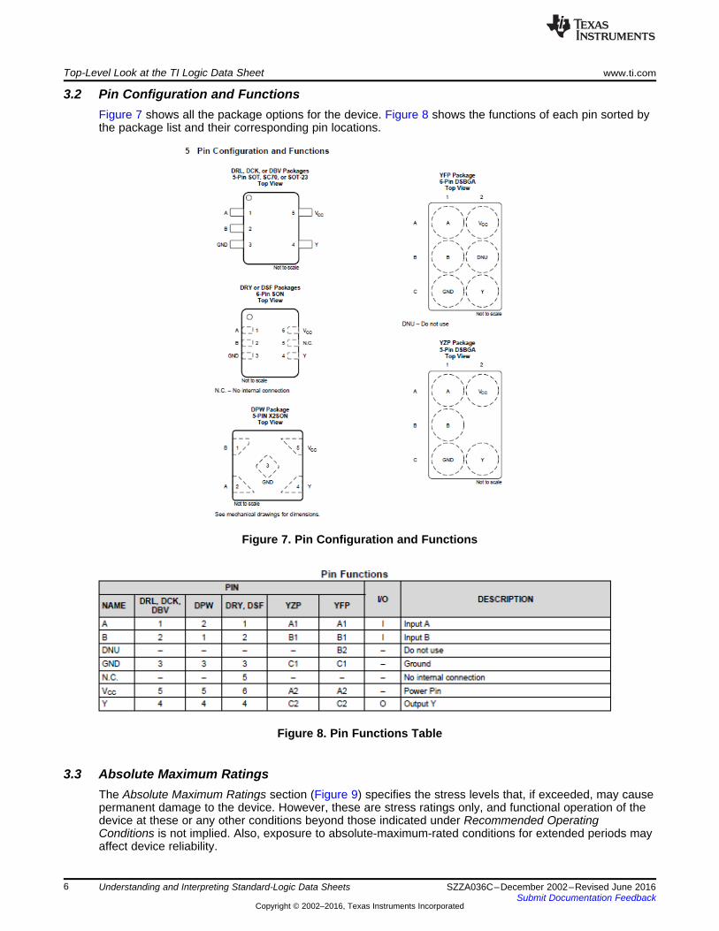
3.2 Pin Configuration and FunctionsFigure 7 shows all the package options for the device. Figure 8 shows the functions of each pin sorted bythe package list and their corresponding pin locations.
Figure 7. Pin Configuration and Functions
Figure 8. Pin Functions Table
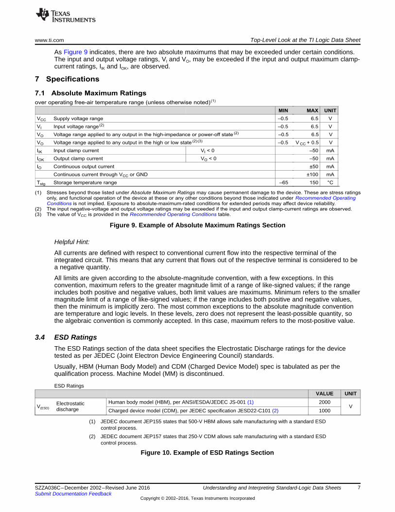
3.3 Absolute Maximum RatingsThe Absolute Maximum Ratings section (Figure 9) specifies the stress levels that, if exceeded, may causepermanent damage to the device. However, these are stress ratings only, and functional operation of thedevice at these or any other conditions beyond those indicated under Recommended OperatingConditions is not implied. Also, exposure to absolute-maximum-rated conditions for extended periods mayaffect device reliability.
7 Specifications
7.1 Absolute Maximum Ratings
over operating free-air temperature range (unless otherwise noted) (1)
VCC Supply voltage range
VI Input voltage range (2)
VO Voltage range applied to any output in the high-impedance or power-off state (2)
VO Voltage range applied to any output in the high or low state (2) (3)
IIK Input clamp current VI < 0
IOK Output clamp current VO < 0
IO Continuous output current
Continuous current through VCC or GND
Tstg Storage temperature range
MIN MAX UNIT
–0.5 6.5 V
–0.5 6.5 V
–0.5 6.5 V
–0.5 V CC + 0.5 V
–50 mA
–50 mA
±50 mA
±100 mA
–65 150 °C
(1) Stresses beyond those listed under Absolute Maximum Ratings may cause permanent damage to the device. These are stress ratingsonly, and functional operation of the device at these or any other conditions beyond those indicated under Recommended OperatingConditions is not implied. Exposure to absolute-maximum-rated conditions for extended periods may affect device reliability.
(2) The input negative-voltage and output voltage ratings may be exceeded if the input and output clamp-current ratings are observed.(3) The value of VCC is provided in the Recommended Operating Conditions table.
www.ti.com Top-Level Look at the TI Logic Data Sheet
7SZZA036C–December 2002–Revised June 2016Submit Documentation Feedback
Copyright © 2002–2016, Texas Instruments Incorporated
Understanding and Interpreting Standard-Logic Data Sheets
As Figure 9 indicates, there are two absolute maximums that may be exceeded under certain conditions.The input and output voltage ratings, VI and VO, may be exceeded if the input and output maximum clamp-current ratings, IIK and IOK, are observed.
Figure 9. Example of Absolute Maximum Ratings Section
Helpful Hint:
All currents are defined with respect to conventional current flow into the respective terminal of theintegrated circuit. This means that any current that flows out of the respective terminal is considered to bea negative quantity.
All limits are given according to the absolute-magnitude convention, with a few exceptions. In thisconvention, maximum refers to the greater magnitude limit of a range of like-signed values; if the rangeincludes both positive and negative values, both limit values are maximums. Minimum refers to the smallermagnitude limit of a range of like-signed values; if the range includes both positive and negative values,then the minimum is implicitly zero. The most common exceptions to the absolute magnitude conventionare temperature and logic levels. In these levels, zero does not represent the least-possible quantity, sothe algebraic convention is commonly accepted. In this case, maximum refers to the most-positive value.
3.4 ESD RatingsThe ESD Ratings section of the data sheet specifies the Electrostatic Discharge ratings for the devicetested as per JEDEC (Joint Electron Device Engineering Council) standards.
Usually, HBM (Human Body Model) and CDM (Charged Device Model) spec is tabulated as per thequalification process. Machine Model (MM) is discontinued.
ESD RatingsVALUE UNIT
V(ESD)Electrostaticdischarge
Human body model (HBM), per ANSI/ESDA/JEDEC JS-001 (1) 2000V
Charged device model (CDM), per JEDEC specification JESD22-C101 (2) 1000
(1) JEDEC document JEP155 states that 500-V HBM allows safe manufacturing with a standard ESDcontrol process.
(2) JEDEC document JEP157 states that 250-V CDM allows safe manufacturing with a standard ESDcontrol process.
Figure 10. Example of ESD Ratings Section
Top-Level Look at the TI Logic Data Sheet www.ti.com
8 SZZA036C–December 2002–Revised June 2016Submit Documentation Feedback
Copyright © 2002–2016, Texas Instruments Incorporated
Understanding and Interpreting Standard-Logic Data Sheets
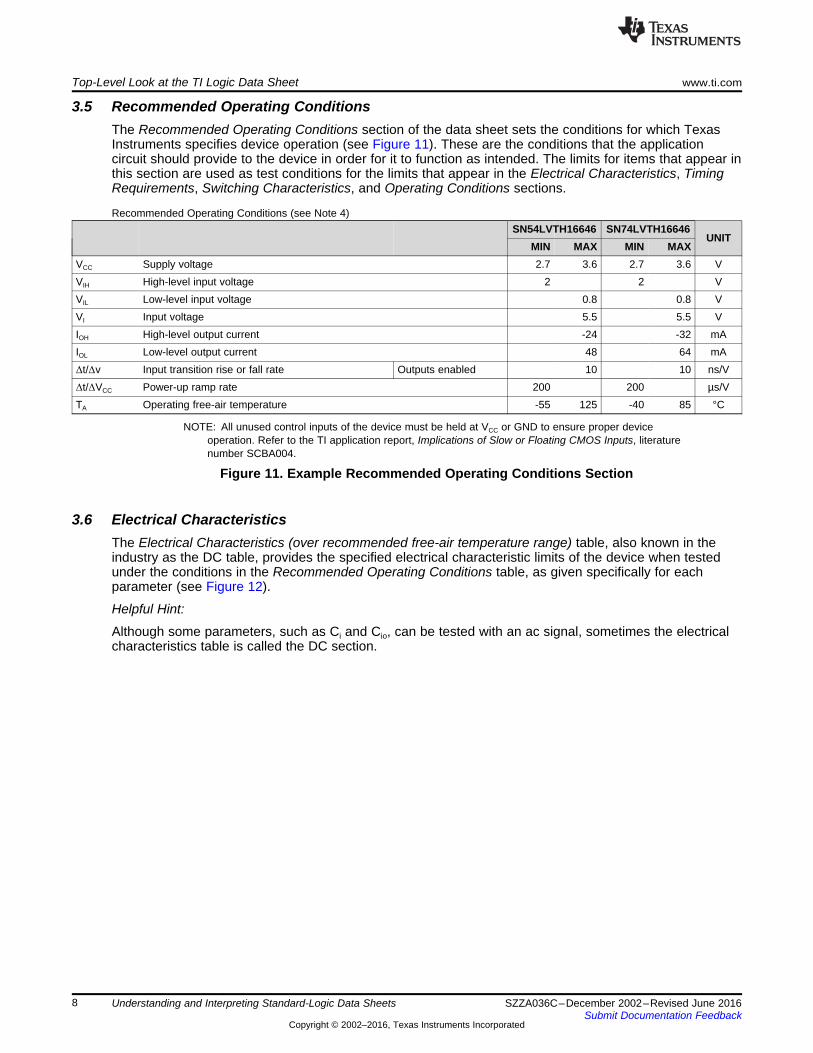
3.5 Recommended Operating ConditionsThe Recommended Operating Conditions section of the data sheet sets the conditions for which TexasInstruments specifies device operation (see Figure 11). These are the conditions that the applicationcircuit should provide to the device in order for it to function as intended. The limits for items that appear inthis section are used as test conditions for the limits that appear in the Electrical Characteristics, TimingRequirements, Switching Characteristics, and Operating Conditions sections.
Recommended Operating Conditions (see Note 4)SN54LVTH16646 SN74LVTH16646
UNITMIN MAX MIN MAX
VCC Supply voltage 2.7 3.6 2.7 3.6 VVIH High-level input voltage 2 2 VVIL Low-level input voltage 0.8 0.8 VVI Input voltage 5.5 5.5 VIOH High-level output current -24 -32 mAIOL Low-level output current 48 64 mAΔt/Δv Input transition rise or fall rate Outputs enabled 10 10 ns/VΔt/ΔVCC Power-up ramp rate 200 200 µs/VTA Operating free-air temperature -55 125 -40 85 °C
NOTE: All unused control inputs of the device must be held at VCC or GND to ensure proper deviceoperation. Refer to the TI application report, Implications of Slow or Floating CMOS Inputs, literaturenumber SCBA004.
Figure 11. Example Recommended Operating Conditions Section
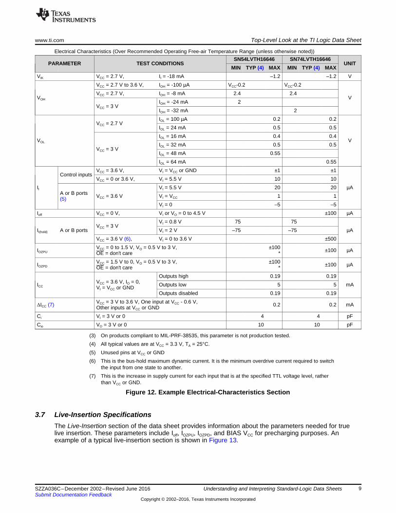
3.6 Electrical CharacteristicsThe Electrical Characteristics (over recommended free-air temperature range) table, also known in theindustry as the DC table, provides the specified electrical characteristic limits of the device when testedunder the conditions in the Recommended Operating Conditions table, as given specifically for eachparameter (see Figure 12).
Helpful Hint:
Although some parameters, such as Ci and Cio, can be tested with an ac signal, sometimes the electricalcharacteristics table is called the DC section.
www.ti.com Top-Level Look at the TI Logic Data Sheet
9SZZA036C–December 2002–Revised June 2016Submit Documentation Feedback
Copyright © 2002–2016, Texas Instruments Incorporated
Understanding and Interpreting Standard-Logic Data Sheets
Electrical Characteristics (Over Recommended Operating Free-air Temperature Range (unless otherwise noted))
PARAMETER TEST CONDITIONSSN54LVTH16646 SN74LVTH16646
UNITMIN TYP (4) MAX MIN TYP (4) MAX
VIK VCC = 2.7 V, II = -18 mA –1.2 –1.2 V
VOH
VCC = 2.7 V to 3.6 V, IOH = -100 µA VCC-0.2 VCC-0.2
VVCC = 2.7 V, IOH = -8 mA 2.4 2.4
VCC = 3 VIOH = -24 mA 2IOH = -32 mA 2
VOL
VCC = 2.7 VIOL = 100 µA 0.2 0.2
V
IOL = 24 mA 0.5 0.5
VCC = 3 V
IOL = 16 mA 0.4 0.4IOL = 32 mA 0.5 0.5IOL = 48 mA 0.55IOL = 64 mA 0.55
II
Control inputsVCC = 3.6 V, VI = VCC or GND ±1 ±1
µAVCC = 0 or 3.6 V, VI = 5.5 V 10 10
A or B ports(5) VCC = 3.6 V
VI = 5.5 V 20 20VI = VCC 1 1VI = 0 –5 –5
Ioff VCC = 0 V, VI or VO = 0 to 4.5 V ±100 µA
II(hold) A or B portsVCC = 3 V
VI = 0.8 V 75 75µAVI = 2 V –75 –75
VCC = 3.6 V (6), VI = 0 to 3.6 V ±500
IOZPUVCC = 0 to 1.5 V, VO = 0.5 V to 3 V,OE = don't care
±100* ±100 µA
IOZPDVCC = 1.5 V to 0, VO = 0.5 V to 3 V,OE = don't care
±100* ±100 µA
ICCVCC = 3.6 V, IO = 0,VI = VCC or GND
Outputs high 0.19 0.19mAOutputs low 5 5
Outputs disabled 0.19 0.19
ΔICC (7) VCC = 3 V to 3.6 V, One input at VCC - 0.6 V,Other inputs at VCC or GND 0.2 0.2 mA
Ci VI = 3 V or 0 4 4 pFCio VO = 3 V or 0 10 10 pF
(3) On products compliant to MIL-PRF-38535, this parameter is not production tested.(4) All typical values are at VCC = 3.3 V, TA = 25°C.(5) Unused pins at VCC or GND(6) This is the bus-hold maximum dynamic current. It is the minimum overdrive current required to switch
the input from one state to another.(7) This is the increase in supply current for each input that is at the specified TTL voltage level, rather
than VCC or GND.
Figure 12. Example Electrical-Characteristics Section
3.7 Live-Insertion SpecificationsThe Live-Insertion section of the data sheet provides information about the parameters needed for truelive insertion. These parameters include Ioff, IOZPU, IOZPD, and BIAS VCC for precharging purposes. Anexample of a typical live-insertion section is shown in Figure 13.

Top-Level Look at the TI Logic Data Sheet www.ti.com
10 SZZA036C–December 2002–Revised June 2016Submit Documentation Feedback
Copyright © 2002–2016, Texas Instruments Incorporated
Understanding and Interpreting Standard-Logic Data Sheets
Live-insertion Specifications for B port Over Recommended Operating Free-air Temperature RangePARAMETER TEST CONDITIONS MIN MAX UNIT
Ioff VCC = 0, BIAS VCC = 0, VI or VO = 0 to 1.5 V 10 µAIOZPU VCC = 0 to 1.5 V, BIAS VCC = 0, VO = 0.5 V to 1.5 V, OE = 0 ±30 µAIOZPD VCC = 1.5 V to 0, BIAS VCC = 0, VO = 0.5 V to 1.5 V, OE = 0 ±30 µA
ICC (BIAS VCC)VCC = 0 to 3.15 V
BIAS VCC = 3.15 V to 3.45 V, VO (B port) = 0 to 1.5 V5 mA
VCC = 3.15 V to 3.45 V 10 µAVO VCC = 0, BIAS VCC = 3.3 V, IO = 0 0.95 1.05 VIO VCC = 0, BIAS VCC = 3.15 V to 3.45 V, VO (B port) = 0.6 V -1 µA
Figure 13. Example Live-Insertion Section
3.8 Timing RequirementsTheTiming Requirements section of the data sheet is similar to the Recommended Operating Conditionssection (see Figure 14). These are timings that the application circuit should provide to the device for it tofunction as intended. This section addresses the timing relationships between transitions of one or moreinput signals that are necessary to ensure device functionality and applies only to sequential-logic devices(for example, flip-flops, latches, and registers).
Timing Requirements (Over Recommended Operating Free-air Temperature Range (unless otherwise noted)) (see Figure 2)SN54LVTH16646 SN74LVTH16646
UNITVCC = 3.3 V± 0.3 V VCC = 2.7 V VCC = 3.3 V
± 0.3 V VCC = 2.7 V
MIN MAX MIN MAX MIN MAX MIN MAXfclock Clock frequency 150 150 150 150 MHztw Pulse duration, CLK high or low 3.3 3.3 3.3 3.3 ns
tsuSetup time,A or B before CLKAB↑ or CLKBA↑
Data high 1.2 1.5 1.2 1.5ns
Data low 2 2.8 2 2.8
thHold time,A or B after CLKAB↑ or CLKBA↑
Data high 0.5 0 0.5 0ns
Data low 0.5 0.5 0.5 0.5
Figure 14. Example Timing-Requirements Section
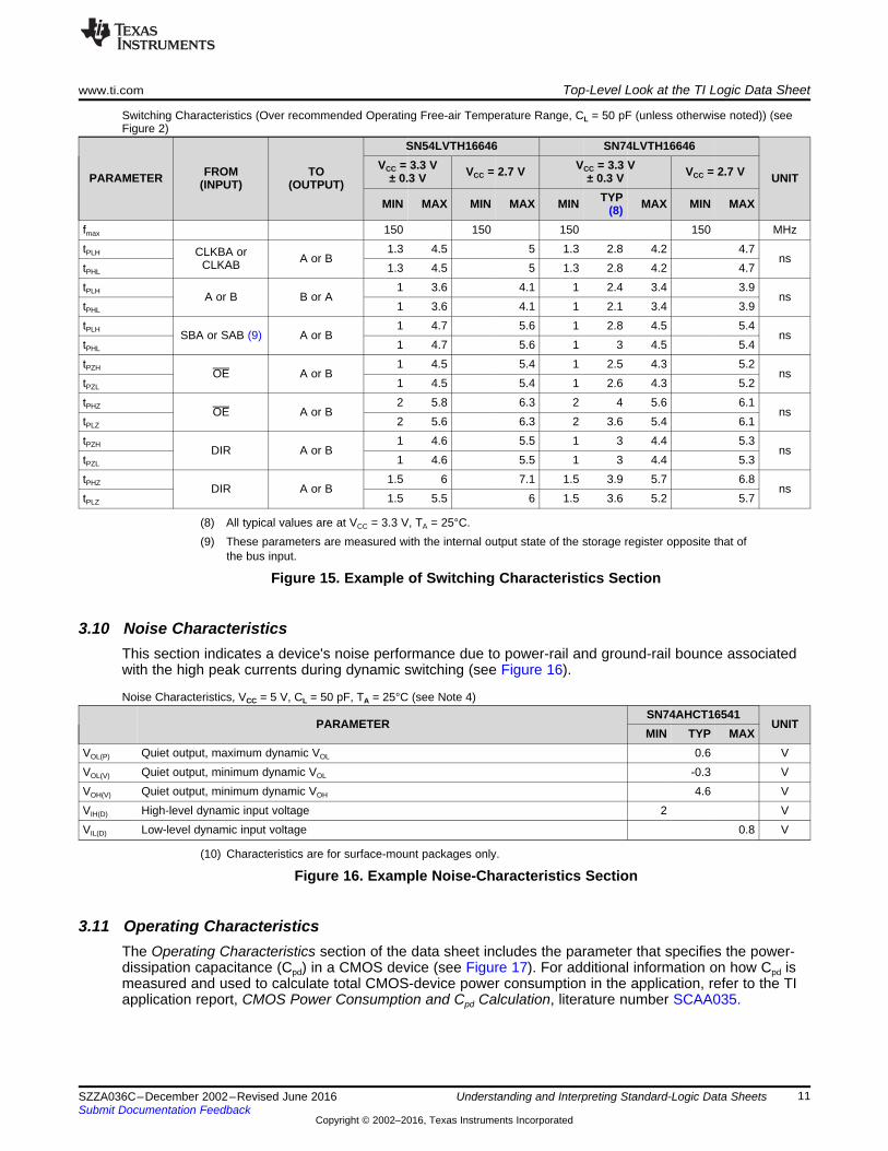
3.9 Switching CharacteristicsThe Switching Characteristics section of the data sheet, also known in the industry as the AC table,includes the parameters that specify how fast the outputs will respond to signal changes at the inputsunder specified conditions of supply voltage, temperature, and load (see Figure 15).
Helpful Hint:
The Switching Characteristics table is sometimes called the AC section, and should not be confused withthe AC small-signal performance because switching characteristics describe the large-signal transientresponse of the circuit.
www.ti.com Top-Level Look at the TI Logic Data Sheet
11SZZA036C–December 2002–Revised June 2016Submit Documentation Feedback
Copyright © 2002–2016, Texas Instruments Incorporated
Understanding and Interpreting Standard-Logic Data Sheets
Switching Characteristics (Over recommended Operating Free-air Temperature Range, CL = 50 pF (unless otherwise noted)) (seeFigure 2)
PARAMETER FROM(INPUT)
TO(OUTPUT)
SN54LVTH16646 SN74LVTH16646
UNITVCC = 3.3 V
± 0.3 V VCC = 2.7 V VCC = 3.3 V± 0.3 V VCC = 2.7 V
MIN MAX MIN MAX MIN TYP(8) MAX MIN MAX
fmax 150 150 150 150 MHztPLH CLKBA or
CLKAB A or B1.3 4.5 5 1.3 2.8 4.2 4.7
nstPHL 1.3 4.5 5 1.3 2.8 4.2 4.7tPLH A or B B or A
1 3.6 4.1 1 2.4 3.4 3.9ns
tPHL 1 3.6 4.1 1 2.1 3.4 3.9tPLH SBA or SAB (9) A or B
1 4.7 5.6 1 2.8 4.5 5.4ns
tPHL 1 4.7 5.6 1 3 4.5 5.4tPZH OE A or B
1 4.5 5.4 1 2.5 4.3 5.2ns
tPZL 1 4.5 5.4 1 2.6 4.3 5.2tPHZ OE A or B
2 5.8 6.3 2 4 5.6 6.1ns
tPLZ 2 5.6 6.3 2 3.6 5.4 6.1tPZH DIR A or B
1 4.6 5.5 1 3 4.4 5.3ns
tPZL 1 4.6 5.5 1 3 4.4 5.3tPHZ DIR A or B
1.5 6 7.1 1.5 3.9 5.7 6.8ns
tPLZ 1.5 5.5 6 1.5 3.6 5.2 5.7
(8) All typical values are at VCC = 3.3 V, TA = 25°C.(9) These parameters are measured with the internal output state of the storage register opposite that of
the bus input.
Figure 15. Example of Switching Characteristics Section
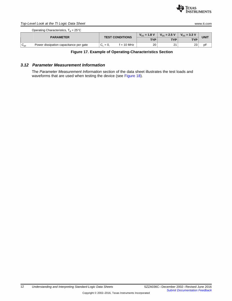
3.10 Noise CharacteristicsThis section indicates a device's noise performance due to power-rail and ground-rail bounce associatedwith the high peak currents during dynamic switching (see Figure 16).
Noise Characteristics, VCC = 5 V, CL = 50 pF, TA = 25°C (see Note 4)
PARAMETERSN74AHCT16541
UNITMIN TYP MAX
VOL(P) Quiet output, maximum dynamic VOL 0.6 VVOL(V) Quiet output, minimum dynamic VOL -0.3 VVOH(V) Quiet output, minimum dynamic VOH 4.6 VVIH(D) High-level dynamic input voltage 2 VVIL(D) Low-level dynamic input voltage 0.8 V
(10) Characteristics are for surface-mount packages only.
Figure 16. Example Noise-Characteristics Section
3.11 Operating CharacteristicsThe Operating Characteristics section of the data sheet includes the parameter that specifies the power-dissipation capacitance (Cpd) in a CMOS device (see Figure 17). For additional information on how Cpd ismeasured and used to calculate total CMOS-device power consumption in the application, refer to the TIapplication report, CMOS Power Consumption and Cpd Calculation, literature number SCAA035.
Top-Level Look at the TI Logic Data Sheet www.ti.com
12 SZZA036C–December 2002–Revised June 2016Submit Documentation Feedback
Copyright © 2002–2016, Texas Instruments Incorporated
Understanding and Interpreting Standard-Logic Data Sheets
Operating Characteristics, TA = 25°C
PARAMETER TEST CONDITIONSVCC = 1.8 V VCC = 2.5 V VCC = 3.3 V
UNITTYP TYP TYP
Cpd Power dissipation capacitance per gate CL = 0, f = 10 MHz 20 21 23 pF
Figure 17. Example of Operating-Characteristics Section
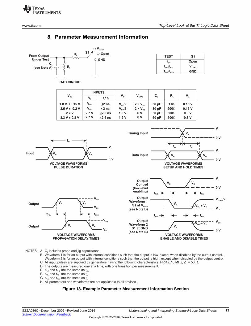
3.12 Parameter Measurement InformationThe Parameter Measurement Information section of the data sheet illustrates the test loads andwaveforms that are used when testing the device (see Figure 18).
2.7 V
thtsu
From OutputUnder Test
C
(see Note A)L
LOAD CIRCUIT
S1
VLOAD
Open
GND
RL
Data Input
Timing Input
0 V
0 V0 V
tW
Input
OutputWaveform 1
S1 at V
(see Note B)LOAD
OutputWaveform 2
S1 at GND(see Note B)
VOL
VOH
0 V
0 V
Output
Output
TEST S1
tpd Open
OutputControl
VM
VM VM
VM
VM
1.8 V 0.15 V±
2.5 V 0.2 V±
2.7 V
3.3 V 0.3 V±
1 kW
500W
500W
500W
VCC RL
2 × VCC
2 × VCC
6 V
VLOAD CL
30 pF
30 pF
50 pF
50 pF
0.15 V
0.15 V
0.3 V
0.3 V
VD
2.7 V
VI
VCC/2
VCC/2
1.5 V
VM
<2 ns
<2 ns
<2.5 ns
<2.5 ns
INPUTS
RL
t / tr f
VCC
VCC
VLOADt /tPLZ PZL
GNDt /tPHZ PZH
VOLTAGE WAVEFORMSENABLE AND DISABLE TIMES
VOLTAGE WAVEFORMSPROPAGATION DELAY TIMES
NOTES: A. C includes probe and jig capacitance.
B. Waveform 1 is for an output with internal conditions such that the output is low, except when disabled by the output control.Waveform 2 is for an output with internal conditions such that the output is high, except when disabled by the output control.
C. All input pulses are supplied by generators having the following characteristics: PRR 10 MHz, Z = 50 .
D. The outputs are measured one at a time, with one transition per measurement.E. t and t are the same as t .
F. t and t are the same as t .
G. t and t are the same as t .
H. All parameters and waveforms are not applicable to all devices.
L
O
PLZ PHZ dis
PZL PZH en
PLH PHL pd
< W
VOLTAGE WAVEFORMSPULSE DURATION
VOLTAGE WAVEFORMSSETUP AND HOLD TIMES
VI
VI
VI
VM
VM
V /2LOAD
tPZL tPLZ
tPHZtPZH
V – VOH D
V + VOL D
VM VM
VOH
VI
VOL
VM
VOL
VOH
VMVM
VM
tPLHtPHL
8 Parameter Measurement Information
1.5 V 6 V
(low-levelenabling)
www.ti.com Top-Level Look at the TI Logic Data Sheet
13SZZA036C–December 2002–Revised June 2016Submit Documentation Feedback
Copyright © 2002–2016, Texas Instruments Incorporated
Understanding and Interpreting Standard-Logic Data Sheets
Figure 18. Example Parameter Measurement Information Section
Dissecting the TI Logic Data Sheet www.ti.com
14 SZZA036C–December 2002–Revised June 2016Submit Documentation Feedback
Copyright © 2002–2016, Texas Instruments Incorporated
Understanding and Interpreting Standard-Logic Data Sheets
4 Dissecting the TI Logic Data SheetIn the following paragraphs, the TI logic data sheet is dissected, and every section and specification isexplained in detail.
4.1 Summary Device Description
4.1.1 Title, Literature Number, and Dates of Origination and Revision
The device number and title appear at the top of every page. The device number is the number of theparent device. The fully qualified part number for a specific device can be found in the Orderable PartNumber table. Figure 19 is a chart to help decode information in the TI logic-device part number.
The literature number is a unique identifier used by TI to identify, store and retrieve a data sheet in internalfiles.
The month and year of origination is the first date of publication of the data sheet. If a data sheet ismodified, the revision date (month and year) is added. If there are multiple revisions, only the latestrevision date appears.
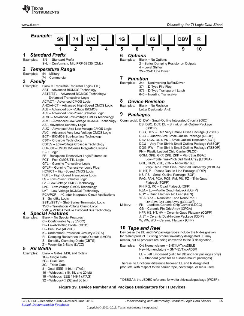
Examples: Blank = Transistor-Transistor Logic (TTL)
ABT – Advanced BiCMOS Technology
ABTE/ETL – Advanced BiCMOS Technology/
Enhanced Transceiver Logic
AC/ACT – Advanced CMOS Logic
AHC/AHCT – Advanced High-Speed CMOS Logic
ALB – Advanced Low-Voltage BiCMOS
ALS – Advanced Low-Power Schottky Logic
ALVC – Advanced Low-Voltage CMOS Technology
ALVT – Advanced Low-Voltage BiCMOS Technology
AS – Advanced Schottky Logic
AUC – Advanced Ultra Low-Voltage CMOS Logic
AVC – Advanced Very Low-Voltage CMOS Logic
BCT – BiCMOS Bus-Interface Technology
CBT – Crossbar Technology
CBTLV – Low-Voltage Crossbar Technology
CD4000 – CMOS B-Series Integrated Circuits
F – F Logic
FB – Backplane Transceiver Logic/Futurebus+
FCT – Fast CMOS TTL Logic
GTL – Gunning Transceiver Logic
GTLP – Gunning Transceiver Logic Plus
HC/HCT – High-Speed CMOS Logic
HSTL – High-Speed Transceiver Logic
LS – Low-Power Schottky Logic
LV – Low-Voltage CMOS Technology
LVC – Low-Voltage CMOS Technology
LVT – Low-Voltage BiCMOS Technology
PCA/PCF – I2C Inter-Integrated Circuit Applications
S – Schottky Logic
SSTL/SSTV – Stub Series-Terminated Logic
TVC – Translation Voltage Clamp Logic
VME – VERSAmodule Eurocard Bus Technology
Examples: Blank = No Special Features
C – Configurable VCC (LVCC)
D – Level-Shifting Diode (CBTD)
H – Bus Hold (ALVCH)
K – Undershoot-Protection Circuitry (CBTK)
R – Damping Resistor on Inputs/Outputs (LVCR)
S – Schottky Clamping Diode (CBTS)
Z – Power-Up 3-State (LVCZ)
Examples: Blank = Gates, MSI, and Octals
1G – Single Gate
2G – Dual Gate
3G – Triple Gate
8 – Octal IEEE 1149.1 (JTAG)
16 – Widebus (16, 18, and 20 bit)
18 – Widebus IEEE 1149.1 (JTAG)
32 – Widebus+ (32 and 36 bit)
Examples: Blank = No Options
2 – Series Damping Resistor on Outputs
4 – Level Shifter
25 – 25-Ω Line Driver
Examples: 244– Noninverting Buffer/Driver
374 – D-Type Flip-Flop
573 – D-Type Transparent Latch
640 – Inverting Transceiver
Examples: Blank = No Revision
Letter Designator A–Z
Commercial: D, DW – Small-Outline Integrated Circuit (SOIC)
DB, DBQ, DCT, DL – Shrink Small-Outline Package
(SSOP)
DBB, DGV – Thin Very Small-Outline Package (TVSOP)
DBQ – Quarter-Size Small-Outline Package (QSOP)
DBV, DCK, DCY, PK – Small-Outline Transistor (SOT)
DCU – Very Thin Shrink Small-Outline Package (VSSOP)
DGG, PW – Thin Shrink Small-Outline Package (TSSOP)
FN – Plastic Leaded Chip Carrier (PLCC)
GGM, GKE, GKF, ZKE, ZKF – MicroStar BGA
Low-Profile Fine-Pitch Ball Grid Array (LFBGA)
GQL, GQN, ZQL, ZQN – MicroStar Jr.
Very-Thin-Profile Fine-Pitch Ball Grid Array (VFBGA)
N, NT, P – Plastic Dual-In-Line Package (PDIP)
NS, PS – Small-Outline Package (SOP)
PAG, PAH, PCA, PCB, PM, PN, PZ – Thin Quad
Flatpack (TQFP)
PH, PQ, RC – Quad Flatpack (QFP)
PZA – Low-Profile Quad Flatpack (LQFP)
RGY – Quad Flatpack No Lead (QFN)
YEA, YZA – NanoStar and NanoFree
Die-Size Ball Grid Array (DSBGA†)
Examples: Old Nomenclature – SN74LVTxxxDBLE
New Nomenclature – SN74LVTxxxADBR
Examples: SN – Standard Prefix
SNJ – Conforms to MIL-PRF-38535 (QML)
Examples: 54– Military
74 – Commercial
Devices in the DB and PW package types include the R designation
for reeled product. Existing product inventory designated LE may
remain, but all products are being converted to the R designation.
There is no functional difference between LE and R designated
products, with respect to the carrier tape, cover tape, or reels used.
LE – Left Embossed (valid for DB and PW packages only)
R – Standard (valid for all surface-mount packages)
Military: FK– Leadless Ceramic Chip Carrier (LCCC)
GB – Ceramic Pin Grid Array (CPGA)
HFP, HS, HT, HV – Ceramic Quad Flatpack (CQFP)
J, JT – Ceramic Dual-In-Line Package (CDIP)
W, WA, WD – Ceramic Flatpack (CFP)
† DSBGAis the JEDEC reference for wafer chip scale package (WCSP).
SN 74 LVC
1 2 3 4 5 6 7 8 9 10
1G 66 DBV R
6 Options
7 Function
8 Device Revision
9 Packages
10 Tape and Reel
1 Standard Prefix
2 Temperature Range
3 Family
4 Special Features
5 Bit Width
Example:
www.ti.com Dissecting the TI Logic Data Sheet
15SZZA036C–December 2002–Revised June 2016Submit Documentation Feedback
Copyright © 2002–2016, Texas Instruments Incorporated
Understanding and Interpreting Standard-Logic Data Sheets
Figure 19. Device Number and Package Designators for TI Devices
VCCA
DIR
A1
•
•
•
•
•
•
•
GND
GND
VCCB
VCCB
OE
B1
•
•
•
•
•
•
•
GND
’4245 Pinning
’LVCC3245
’LVCC4245
No Internal Connection
’245 Pinning
’424
Copyright © 2016, Texas Instruments Incorporated
Dissecting the TI Logic Data Sheet www.ti.com
16 SZZA036C–December 2002–Revised June 2016Submit Documentation Feedback
Copyright © 2002–2016, Texas Instruments Incorporated
Understanding and Interpreting Standard-Logic Data Sheets
Special features of TI standard logic devices are designated in the device number by abbreviations, asshown in the following list and defined in the following paragraphs.• Blank - No special features• C - Configurable VCC
• D - Level-shifting diode• H - Bus hold• K - Undershoot-protection circuitry• R - Damping resistor on inputs/outputs• S - Schottky clamping diode• Z - Power-up 3-state
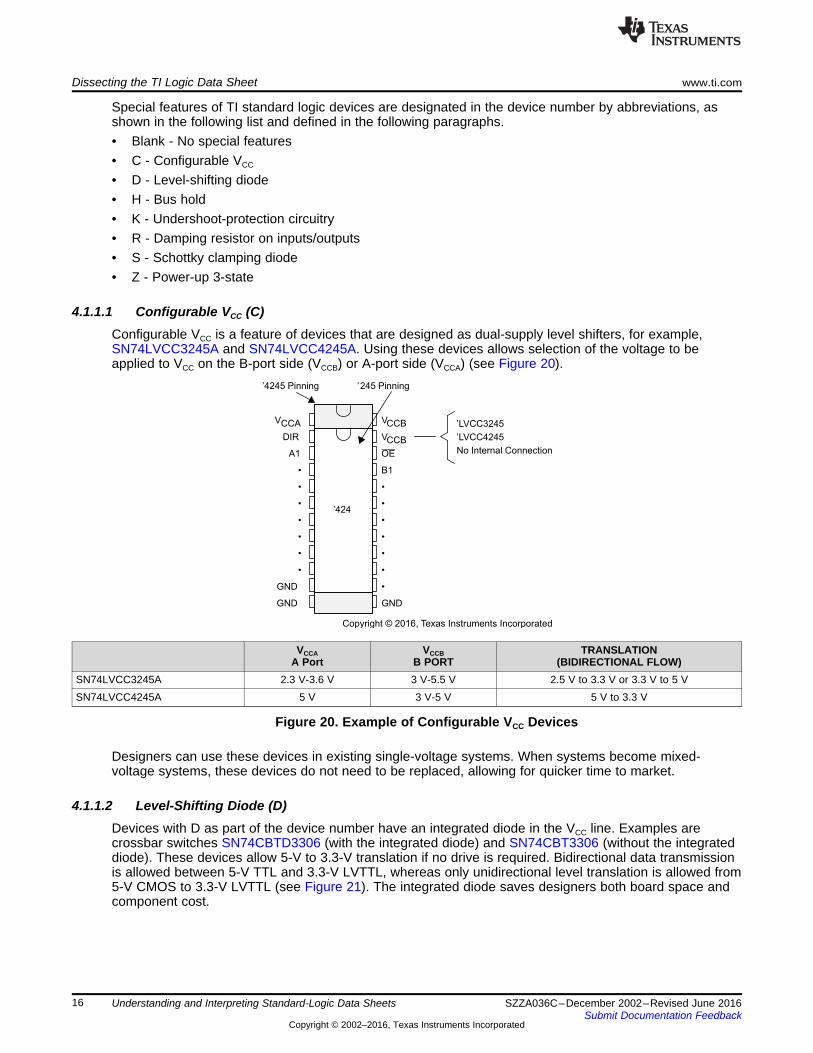
4.1.1.1 Configurable VCC (C)Configurable VCC is a feature of devices that are designed as dual-supply level shifters, for example,SN74LVCC3245A and SN74LVCC4245A. Using these devices allows selection of the voltage to beapplied to VCC on the B-port side (VCCB) or A-port side (VCCA) (see Figure 20).
VCCAA Port
VCCBB PORT
TRANSLATION(BIDIRECTIONAL FLOW)
SN74LVCC3245A 2.3 V-3.6 V 3 V-5.5 V 2.5 V to 3.3 V or 3.3 V to 5 VSN74LVCC4245A 5 V 3 V-5 V 5 V to 3.3 V
Figure 20. Example of Configurable VCC Devices
Designers can use these devices in existing single-voltage systems. When systems become mixed-voltage systems, these devices do not need to be replaced, allowing for quicker time to market.
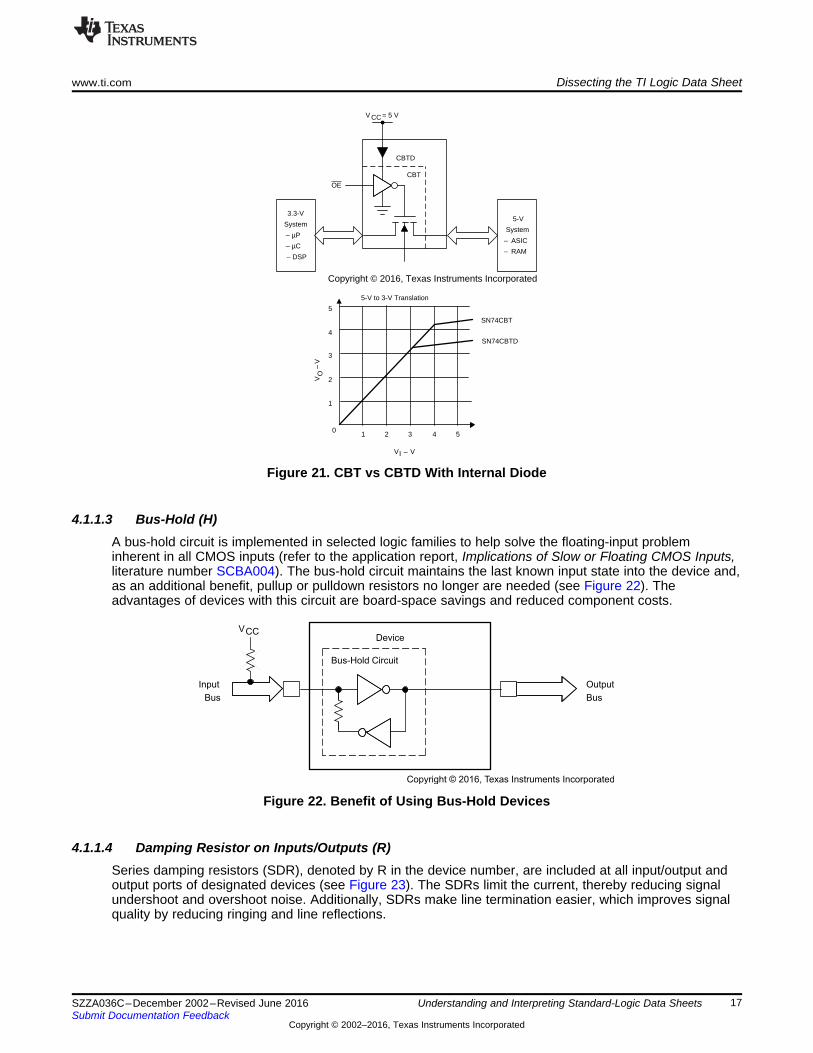
4.1.1.2 Level-Shifting Diode (D)Devices with D as part of the device number have an integrated diode in the VCC line. Examples arecrossbar switches SN74CBTD3306 (with the integrated diode) and SN74CBT3306 (without the integrateddiode). These devices allow 5-V to 3.3-V translation if no drive is required. Bidirectional data transmissionis allowed between 5-V TTL and 3.3-V LVTTL, whereas only unidirectional level translation is allowed from5-V CMOS to 3.3-V LVTTL (see Figure 21). The integrated diode saves designers both board space andcomponent cost.
Bus-Hold Circuit
DeviceVCC
Input
Bus
Output
Bus
Copyright © 2016, Texas Instruments Incorporated
VI ± V
1
2
3
4
5
1
0
5-V to 3-V Translation
SN74CBT
SN74CBTD
VO±
V
2 3 4 5
CBTD
CBT
OE
3.3-V
System
± µP
± µC
± DSP
V CC = 5 V
5-V
System
± ASIC
± RAM
Copyright © 2016, Texas Instruments Incorporated
www.ti.com Dissecting the TI Logic Data Sheet
17SZZA036C–December 2002–Revised June 2016Submit Documentation Feedback
Copyright © 2002–2016, Texas Instruments Incorporated
Understanding and Interpreting Standard-Logic Data Sheets
Figure 21. CBT vs CBTD With Internal Diode
4.1.1.3 Bus-Hold (H)A bus-hold circuit is implemented in selected logic families to help solve the floating-input probleminherent in all CMOS inputs (refer to the application report, Implications of Slow or Floating CMOS Inputs,literature number SCBA004). The bus-hold circuit maintains the last known input state into the device and,as an additional benefit, pullup or pulldown resistors no longer are needed (see Figure 22). Theadvantages of devices with this circuit are board-space savings and reduced component costs.
Figure 22. Benefit of Using Bus-Hold Devices
4.1.1.4 Damping Resistor on Inputs/Outputs (R)Series damping resistors (SDR), denoted by R in the device number, are included at all input/output andoutput ports of designated devices (see Figure 23). The SDRs limit the current, thereby reducing signalundershoot and overshoot noise. Additionally, SDRs make line termination easier, which improves signalquality by reducing ringing and line reflections.
1A 1B
1OE
Copyright © 2016, Texas Instruments Incorporated
From InternalOutput
SDR
Logic Circuitry
VCC
Copyright © 2016, Texas Instruments Incorporated
Dissecting the TI Logic Data Sheet www.ti.com
18 SZZA036C–December 2002–Revised June 2016Submit Documentation Feedback
Copyright © 2002–2016, Texas Instruments Incorporated
Understanding and Interpreting Standard-Logic Data Sheets
Figure 23. Series-Damping-Resistor Option
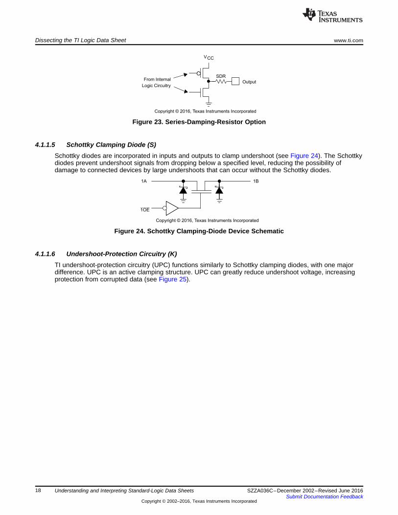
4.1.1.5 Schottky Clamping Diode (S)Schottky diodes are incorporated in inputs and outputs to clamp undershoot (see Figure 24). The Schottkydiodes prevent undershoot signals from dropping below a specified level, reducing the possibility ofdamage to connected devices by large undershoots that can occur without the Schottky diodes.
Figure 24. Schottky Clamping-Diode Device Schematic
4.1.1.6 Undershoot-Protection Circuitry (K)TI undershoot-protection circuitry (UPC) functions similarly to Schottky clamping diodes, with one majordifference. UPC is an active clamping structure. UPC can greatly reduce undershoot voltage, increasingprotection from corrupted data (see Figure 25).
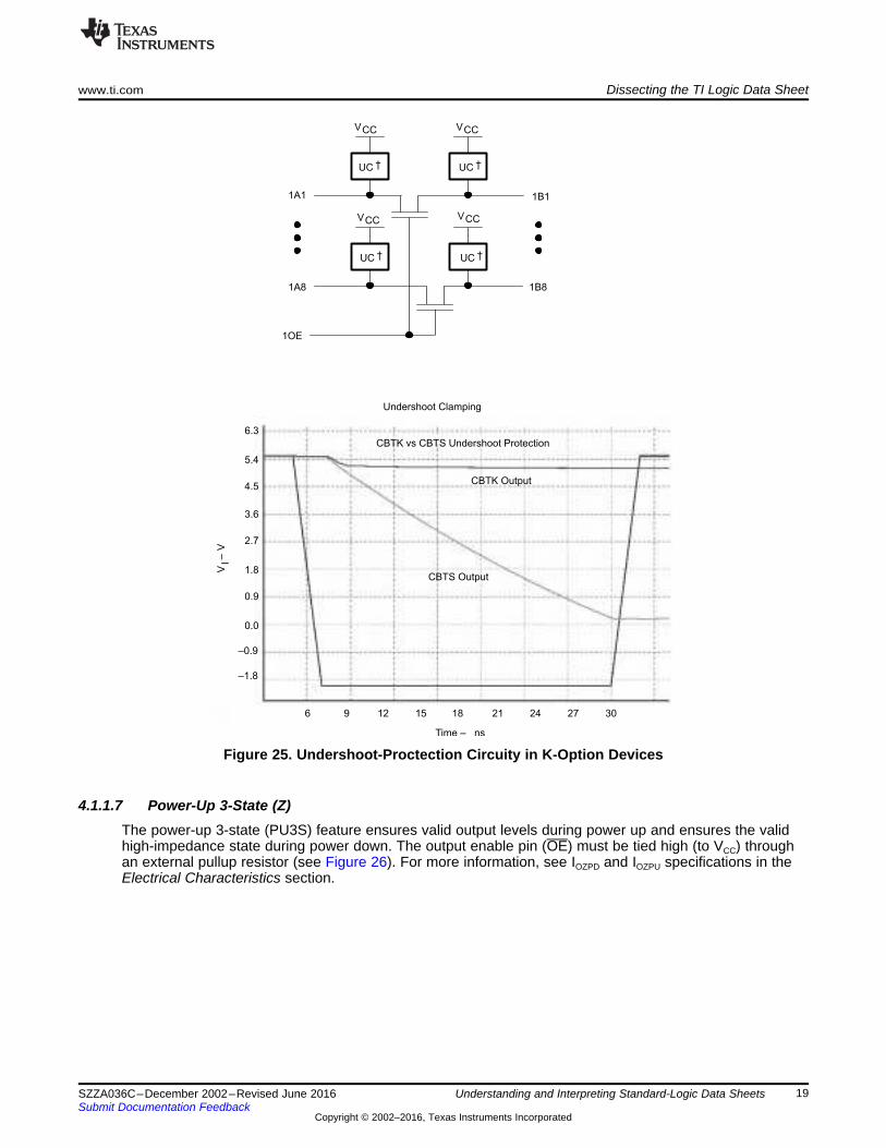
Undershoot Clamping
6.3
5.4
4.5
3.6
2.7
1.8
0.9
0.0
–0.9
–1.8
6 9 12 15 18 21 24 27 30
Time – ns
CBTS Output
CBTK Output
CBTK vs CBTS Undershoot Protection
VI–
V
1A1
1A8
1OE
VCCVCC
VCC VCC
1B8
1B1
UC † UC †
UC † UC †
www.ti.com Dissecting the TI Logic Data Sheet
19SZZA036C–December 2002–Revised June 2016Submit Documentation Feedback
Copyright © 2002–2016, Texas Instruments Incorporated
Understanding and Interpreting Standard-Logic Data Sheets
Figure 25. Undershoot-Proctection Circuity in K-Option Devices
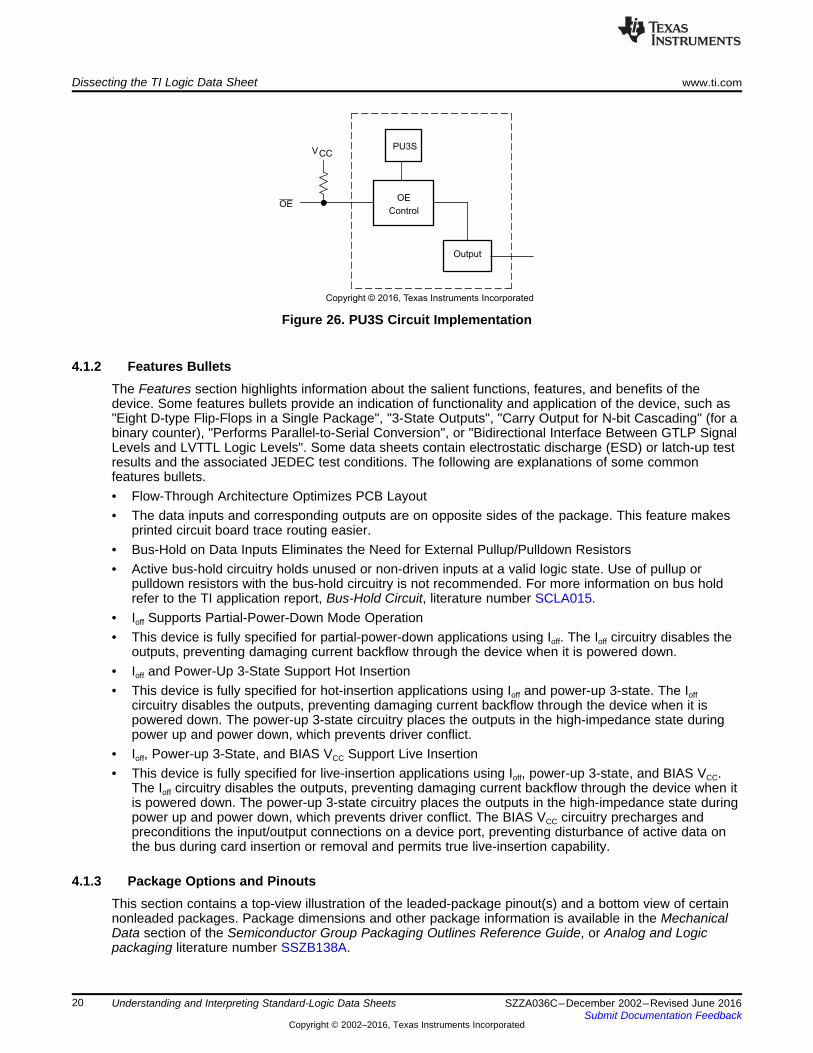
4.1.1.7 Power-Up 3-State (Z)The power-up 3-state (PU3S) feature ensures valid output levels during power up and ensures the validhigh-impedance state during power down. The output enable pin (OE) must be tied high (to VCC) throughan external pullup resistor (see Figure 26). For more information, see IOZPD and IOZPU specifications in theElectrical Characteristics section.
PU3S
Output
VCC
OEOE
Control
Copyright © 2016, Texas Instruments Incorporated
Dissecting the TI Logic Data Sheet www.ti.com
20 SZZA036C–December 2002–Revised June 2016Submit Documentation Feedback
Copyright © 2002–2016, Texas Instruments Incorporated
Understanding and Interpreting Standard-Logic Data Sheets
Figure 26. PU3S Circuit Implementation
4.1.2 Features BulletsThe Features section highlights information about the salient functions, features, and benefits of thedevice. Some features bullets provide an indication of functionality and application of the device, such as"Eight D-type Flip-Flops in a Single Package", "3-State Outputs", "Carry Output for N-bit Cascading" (for abinary counter), "Performs Parallel-to-Serial Conversion", or "Bidirectional Interface Between GTLP SignalLevels and LVTTL Logic Levels". Some data sheets contain electrostatic discharge (ESD) or latch-up testresults and the associated JEDEC test conditions. The following are explanations of some commonfeatures bullets.• Flow-Through Architecture Optimizes PCB Layout• The data inputs and corresponding outputs are on opposite sides of the package. This feature makes
printed circuit board trace routing easier.• Bus-Hold on Data Inputs Eliminates the Need for External Pullup/Pulldown Resistors• Active bus-hold circuitry holds unused or non-driven inputs at a valid logic state. Use of pullup or
pulldown resistors with the bus-hold circuitry is not recommended. For more information on bus holdrefer to the TI application report, Bus-Hold Circuit, literature number SCLA015.
• Ioff Supports Partial-Power-Down Mode Operation• This device is fully specified for partial-power-down applications using Ioff. The Ioff circuitry disables the
outputs, preventing damaging current backflow through the device when it is powered down.• Ioff and Power-Up 3-State Support Hot Insertion• This device is fully specified for hot-insertion applications using Ioff and power-up 3-state. The Ioff
circuitry disables the outputs, preventing damaging current backflow through the device when it ispowered down. The power-up 3-state circuitry places the outputs in the high-impedance state duringpower up and power down, which prevents driver conflict.
• Ioff, Power-up 3-State, and BIAS VCC Support Live Insertion• This device is fully specified for live-insertion applications using Ioff, power-up 3-state, and BIAS VCC.
The Ioff circuitry disables the outputs, preventing damaging current backflow through the device when itis powered down. The power-up 3-state circuitry places the outputs in the high-impedance state duringpower up and power down, which prevents driver conflict. The BIAS VCC circuitry precharges andpreconditions the input/output connections on a device port, preventing disturbance of active data onthe bus during card insertion or removal and permits true live-insertion capability.
4.1.3 Package Options and PinoutsThis section contains a top-view illustration of the leaded-package pinout(s) and a bottom view of certainnonleaded packages. Package dimensions and other package information is available in the MechanicalData section of the Semiconductor Group Packaging Outlines Reference Guide, or Analog and Logicpackaging literature number SSZB138A.
Current: SN74 ALVCH R 16 2 245 ANew: SN74 ALVCH R 16 245 A
Input/Output Resistor
Output Resistor
www.ti.com Dissecting the TI Logic Data Sheet
21SZZA036C–December 2002–Revised June 2016Submit Documentation Feedback
Copyright © 2002–2016, Texas Instruments Incorporated
Understanding and Interpreting Standard-Logic Data Sheets
4.1.4 ApplicationsThe Applications section contains a list of the typical system applications the device can used in.
4.1.5 DescriptionThe Description section contains a written detailed explanation of the functionality and features of thedevice.
4.1.6 BGA Packaging Top-View Illustrations and Pin-Assignments TableThis section contains the top-view illustrations and pin assignments for applicable BGA package types.
4.1.7 Device InformationA table is provided that gives the fully qualified orderable part number and topside symbolization for everypackage option of the device.
TI has converted to an advanced order-entry system that provides significant improvements to all facets ofTI business, from production, to order entry, to logistics. One requirement is a limitation of TI part numbersto no more than 18 characters. Based on customer inputs, TI determined that the least-disruptiveimplementations would be as outlined below:1. Package alias
TI uses an alias to denote specific packages for device numbers that exceed 18 characters. Table 1shows a mapping of package codes to an alias representation.
Table 1. Package Alias
CurrentPackage Code Alias
DL LDGG/DBB GDGV VGKE/GKF/GQL KDLR LR - tape/reel packingDGGR/DBBR GR - tape/reel packingDGVR VR - tape/reel packingGKER/GKFR/GQLR KR - tape/reel packing
2. Resistor-option nomenclatureFor device numbers of more than 18 characters and with input and output resistors, TI has adopted asimplified nomenclature to designate the resistor option. This eliminates the redundant "2" (designatingoutput resistors) when the part number also contains an "R" (designating input/output resistors).
There is no change to the device or data sheet electrical parameters. The packages involved and thechanges in nomenclature are given in Table 1.
The approximate body size in millimeters are given for each of the package .
4.1.8 Function TableThe function table illustrates the expected logic values on the outputs, when the inputs have the givenstimuli applied.
The following symbols are used in function tables in TI data sheets:
H = high level (steady state)
L = low level (steady state)
↑ = transition from low to high level
↓ = transition from high to low level
= value/level or resulting value/level is routed to indicated destination
= value/level is re-entered
X = irrelevant (any input, including transitions)
Z = off (high-impedance) state of a 3-state output
a . . . h = the level of steady-state inputs A through H, respectively
Q0 = level of Q before the indicated steady-state input conditions were established
Toggle = each output changes to the complement of its previous level on each active
transition indicated by ↓or ↑
Q0 = complement of Q0 or level of Q before the indicated steady-state input
conditions were established
Qn = level of Q before the most-recent active transition indicated by ↓or ↑
= one high-level pulse
= one low-level pulse
Dissecting the TI Logic Data Sheet www.ti.com
22 SZZA036C–December 2002–Revised June 2016Submit Documentation Feedback
Copyright © 2002–2016, Texas Instruments Incorporated
Understanding and Interpreting Standard-Logic Data Sheets
In the input columns, if a row contains only the symbols H, L, or X, the indicated output is valid when theinput configuration is achieved, regardless of the sequence in which it is achieved. The output persists aslong as the input configuration is maintained.
In the input columns, if a row contains H, L, and/or X, together with ↑ and/or ↓, the output is valid when theinput configuration is achieved, but the transition(s) must occur after steady-state levels are attained. If theoutput is shown as a level (H, L, Q0, or Q0 ), it persists as long as the steady-state input levels and thelevels that terminate indicated transitions are maintained. Unless otherwise indicated, input transitions inthe opposite direction to those shown have no effect at the output. If the output is shown as a pulse, "-" ,or "- -", the pulse follows the indicated input transition and persists for an interval that is dependent on thecircuit.
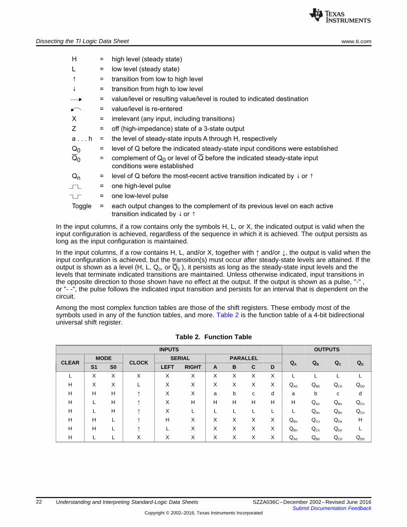
Among the most complex function tables are those of the shift registers. These embody most of thesymbols used in any of the function tables, and more. Table 2 is the function table of a 4-bit bidirectionaluniversal shift register.
Table 2. Function Table
INPUTS OUTPUTS
CLEARMODE
CLOCKSERIAL PARALLEL
QA QB QC QDS1 S0 LEFT RIGHT A B C DL X X X X X X X X X L L L LH X X L X X X X X X QA0 QB0 QC0 QD0
H H H ↑ X X a b c d a b c dH L H ↑ X H H H H H H QAn QBn QCn
H L H ↑ X L L L L L L QAn QBn QCn
H H L ↑ H X X X X X QBn QCn QDn HH H L ↑ L X X X X X QBn QCn QDn LH L L X X X X X X X QA0 QB0 QC0 QD0
www.ti.com Dissecting the TI Logic Data Sheet
23SZZA036C–December 2002–Revised June 2016Submit Documentation Feedback
Copyright © 2002–2016, Texas Instruments Incorporated
Understanding and Interpreting Standard-Logic Data Sheets
The first row of the table represents a synchronous clearing of the register and states that, if clear is low,all four outputs will be reset low, regardless of the other inputs, which are denoted by X. In the followingrows, clear is inactive (high); therefore, it has no effect.
The second row shows that, as long as the clock input remains low (while clear is high), no other inputhas any effect, and the outputs maintain the levels they assumed before the steady-state combination ofclear high and clock low was established. Because, on other rows of the table only the rising transition ofthe clock is shown to be active, the second row implicitly shows that no further change in the outputsoccurs while the clock remains high or on the high-to-low transition of the clock.
The third row of the table represents synchronous parallel loading of the register and states that if S1 andS0 are both high, then, without regard to the serial input, the data entered at A is at output QA, dataentered at B is at QB, and so forth, following a low-to-high clock transition.
The fourth and fifth rows represent the loading of high- and low-level data, respectively, from the shift-rightserial input and the shifting of previously entered data one bit; data previously at QA is now at QB, theprevious levels of QB and QC are now at QC and QD, respectively, and the data previously at QD no longeris in the register. This entry of serial data and shift takes place on the low-to-high transition of the clockwhen S1 is low and S0 is high, and the levels at inputs A through D have no effect.
The sixth and seventh rows represent the loading of high- and low-level data, respectively, from the shift-left serial input and the shifting of previously entered data one bit; data previously at QB is now at QA, theprevious levels of QC and QD now are at QB and QC, respectively, and the data previously at QA no longeris in the register. This entry of serial data and shift takes place on the low-to-high transition of the clockwhen S1 is high and S0 is low, and the levels at inputs A through D have no effect.
The last row shows that, as long as both inputs are low, no other input has any effect and, as in thesecond row, the outputs maintain the levels they assumed before the steady-state combination of clearhigh and both mode inputs low was established.
The function table functional tests do not reflect all possible combinations or sequential modes.
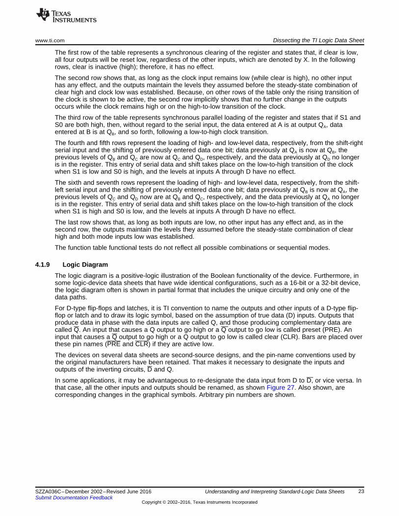
4.1.9 Logic DiagramThe logic diagram is a positive-logic illustration of the Boolean functionality of the device. Furthermore, insome logic-device data sheets that have wide identical configurations, such as a 16-bit or a 32-bit device,the logic diagram often is shown in partial format that includes the unique circuitry and only one of thedata paths.
For D-type flip-flops and latches, it is TI convention to name the outputs and other inputs of a D-type flip-flop or latch and to draw its logic symbol, based on the assumption of true data (D) inputs. Outputs thatproduce data in phase with the data inputs are called Q, and those producing complementary data arecalled Q. An input that causes a Q output to go high or a Q output to go low is called preset (PRE). Aninput that causes a Q output to go high or a Q output to go low is called clear (CLR). Bars are placed overthese pin names (PRE and CLR) if they are active low.
The devices on several data sheets are second-source designs, and the pin-name conventions used bythe original manufacturers have been retained. That makes it necessary to designate the inputs andoutputs of the inverting circuits, D and Q.
In some applications, it may be advantageous to re-designate the data input from D to D, or vice versa. Inthat case, all the other inputs and outputs should be renamed, as shown Figure 27. Also shown, arecorresponding changes in the graphical symbols. Arbitrary pin numbers are shown.
S1
C12
C
6
Q5
C1
1D3
D
R4
Latch
PRE
CLR
Q
S1
2CLK
6
Q5
1D3
D
R4
Flip-Flop
PRE
CLR
Q
R1
C12
C
5
Q6
C1
1D3
S4
Latch
Q6
5
Flip-Flop
PRE
CLRQ
Q
D
R1
2CLK
1D3
S4
PRE
CLR
D
Copyright © 2016, Texas Instruments Incorporated
Dissecting the TI Logic Data Sheet www.ti.com
24 SZZA036C–December 2002–Revised June 2016Submit Documentation Feedback
Copyright © 2002–2016, Texas Instruments Incorporated
Understanding and Interpreting Standard-Logic Data Sheets
Figure 27. Example Logic Diagram
The figures show that when Q and Q exchange names, the preset and clear pins also exchange names.The polarity indicators ( ) on PRE and CLR remain, as these inputs still are active low, but thepresence or absence of the polarity indicator changes at D (or D), Q, and Q. Pin 5 (Q or Q) is still in phasewith the data input (D or D); their active levels change together.
4.1.10 Product Development Stage NoteThe product development stage note is a standard disclaimer placed at the lower left corner of the firstpage of data sheets, and the words ADVANCED INFORMATION or PRODUCT PREVIEW, as applicable,appear in the left and right margins of all pages of the data sheet. There is only the product developmentstage note on the first page for production-data devices. For additional information, see the EIA/JEDECengineering publication, Suggested Product-Documentation Classifications and Disclaimers, JEP103A.
4.1.11 Table Of ContentsThe Table of Contents section provides the outline for the data sheet with each section and a hyperlinkwhich when clicked to take directly to the specified page.
4.2 Revision HistoryThe changes for the data sheet compared to previous revision is mentioned in a tabular format along withthe pages affected in the Revision History.
4.3 Pin Configuration And FunctionsEach of the packages top view or the bottom view (whenever applicable) is shown along with a tabularrepresentation of the name of each pin , the pin position in each of the packages and the description ofeach pin. Each pin being input , output , Input /Output , power or ground pin is also mentioned in the sametable.
4.4 Absolute Maximum Ratings
4.4.1 Supply Voltage, VCC
This is the maximum voltage that can be applied safely to the VCC terminal, with respect to the ground ofthe device. However, no data sheet parameters are ensured when a device is operated at the absolutemaximum VCC level.
Power
Clamp
Ground
Clamp
Power
Clamp
Ground
Clamp
LogicInput Output
VCC
GND
Copyright © 2016, Texas Instruments Incorporated
www.ti.com Dissecting the TI Logic Data Sheet
25SZZA036C–December 2002–Revised June 2016Submit Documentation Feedback
Copyright © 2002–2016, Texas Instruments Incorporated
Understanding and Interpreting Standard-Logic Data Sheets
4.4.2 Input Voltage, VI
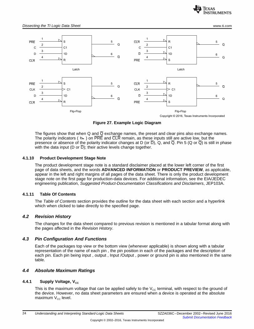
This is the maximum voltage that can be applied safely to an input terminal, with respect to the ground ofthe device. This maximum VI specification may be exceeded if the output clamp rating, IIK, is observed.
Helpful Hint:
If there are clamp diodes between the device inputs and the VCC supply (see Figure 28) for ESD protectionor overshoot clamping, the positive absolute-maximum rating for the input voltage is specified as VCC + 0.5V. Keeping the applied input voltage less than 0.5 V above VCC ensures that there will not be enoughvoltage across the clamp diode to forward-bias it and cause current to flow through it. The TI logic familieswith clamp diodes in the inputs are: AC, ACT, AHC, AHCT, ALB, ALS, ALVC, AS, F, (CD)FCT, HC, HCT,HSTL, LS, PCA, PCF, S, SSTL, and TTL.
If there are no clamp diodes between the device inputs and the VCC supply, the positive absolutemaximum rating is a limitation of the process technology and is specified as an absolute voltage (forexample, 5.5 V). The TI logic families without clamp diodes in the inputs are: ABT, ABTE, ALS, ALVT,AUC, AVC, BCT, FB, GTLP, GTL, LS, LV, LVC, LVCZ, LVT, (CY)FCT, SSTV, and VME.
You may exceed the negative input-voltage rating if you ensure that you are not putting too much currentthrough the ground-clamp diode. The IIK absolute maximum rating specifies the maximum current that maybe put through the ground-clamp diode.
Figure 28. Representation of Typical Logic I/O Clamping Circuits
4.4.3 Output Voltage, VO
This is the maximum voltage that can be applied safely to an output terminal, with respect to the ground ofthe device.
Helpful Hint:
If there are clamp diodes between the device outputs and the VCC supply (see Figure 28) for ESDprotection or parasitic current paths in the output p-channel pullup transistor, the positive absolutemaximum rating for the output voltage is specified as VCC + 0.5 V. This ensures that there will not beenough voltage applied between the output and VCC to forward bias the clamp diode and cause current toflow. You may exceed the negative rating if you ensure that you are not putting too much current throughthe ground-clamp diode. The maximum current that you may put through the ground-clamp diode isspecified in the IOK absolute maximum rating.
If there are no clamp diodes or parasitic current paths in the output P-channel pullup transistor betweenthe device outputs and the VCC supply, the positive absolute maximum rating is a limitation of the processtechnology and is specified as an absolute voltage.
Dissecting the TI Logic Data Sheet www.ti.com
26 SZZA036C–December 2002–Revised June 2016Submit Documentation Feedback
Copyright © 2002–2016, Texas Instruments Incorporated
Understanding and Interpreting Standard-Logic Data Sheets
4.4.4 Voltage Range Applied to Any Output in the High-Impedance or Power-Off State, VO
This specification is similar to the Output Voltage, VO specification and is used with the Voltage RangeApplied to Any Output in the High State, VO specification. On devices with the Ioff feature, there are noclamp diodes or parasitic current paths in the output P-channel pullup transistor between the deviceoutputs and the VCC supply; the positive absolute-maximum rating is a limitation of the process technologyand is specified as an absolute voltage. You may exceed the negative rating if you ensure that you are notputting too much current through the ground-clamp diode. The maximum current that you may put throughthe ground-clamp diode is specified in the IOK absolute-maximum rating.
Helpful Hint:
This specification is necessary only for devices with the Ioff feature.
4.4.5 Voltage Range Applied to Any Output in the High State, VO
This specification is similar to the Output Voltage, VO specification and is used with the Voltage RangeApplied to Any Output in the High-Impedance or Power-Off State, VO specification. When the output isenabled and is in the output high state, there is a current path between the output and VCC through theoutput P-channel pullup transistor. Applying a voltage to the output that is greater than the VCC voltagecauses damaging current to flow back from the output into the VCC supply. You may exceed the negativerating if you ensure that you are not putting too much current through the power-clamp diode. The IOKabsolute-maximum rating specifies the maximum current that you may put through the ground-clampdiode.
Helpful Hint:
This specification is necessary only for devices with the Ioff feature.
4.4.6 Input Clamp Current, IIK
This is the maximum current that can flow safely into an input terminal of the device at voltages above orbelow the normal operating range.
Helpful Hint:
If there are clamp diodes between the device inputs and the VCC supply (see Figure 28), for ESDprotection or overshoot clamping, there will be both a positive and negative absolute maximum rating forthe input clamp current. If there is only a negative absolute maximum rating, that implies that there is onlya ground-clamp diode at the input, not a power-clamp diode.
4.4.7 Output Clamp Current, IOK
This is the maximum current that can flow safely into an output terminal of the device at voltages above orbelow the normal operating range.
Helpful Hint:
If there are clamp diodes between the device outputs and the VCC supply (see Figure 28), for ESDprotection or parasitic current paths in the output P-channel pullup transistor, there will be both a positiveand a negative absolute-maximum rating for the output clamp current. If there is only a negative absolute-maximum rating, that implies that there is only a ground-clamp diode at the output, not a power-clampdiode or a parasitic current path in the output P-channel pullup transistor.
4.4.8 Continuous Output Current, IO
This is the maximum output source or sink current that can flow safely into an output terminal of thedevice at voltages within the normal operating range.
4.4.9 Continuous Current Through VCC or GND TerminalsThis is the maximum current that can flow safely into the VCC or GND terminals of the integrated circuit.
www.ti.com Dissecting the TI Logic Data Sheet
27SZZA036C–December 2002–Revised June 2016Submit Documentation Feedback
Copyright © 2002–2016, Texas Instruments Incorporated
Understanding and Interpreting Standard-Logic Data Sheets
4.4.10 Package Thermal Impedance, Junction-to-Ambient, ΘJA
This is the thermal resistance from the operating portion of a semiconductor device to a natural convection(still air) environment surrounding the device. Tested per JEDEC Standard JESD51-3. For additionalinformation, refer to the TI Application Report; Thermal Characteristics of Standard Linear and Logic (SLL)Packages and Devices, literature number SCZA005.
4.4.11 Storage Temperature Range, Tstg
This is the range of temperatures over which a device can be stored without causing excessivedegradation of its performance characteristics. Typically, the junction temperature TJ is the same asstorage temperature.
4.5 Recommended Operating Conditions
4.5.1 VCC Supply VoltageJEDEC - The supply voltage applied to a circuit connected to the reference terminal.
TI - The range of supply voltages for which operation of the logic element is specified.
The example in Figure 11 lists 2.7 V as the minimum VCC. No electrical or switching characteristic isspecified for VCC less than 2.7 V. Operation outside of the minimum and maximum values is notrecommended, and a previously established logic state might not be maintained under such conditions.
Helpful Hint:
Frequently, TI receives requests from customers wanting assurance that TI logic devices will operateproperly outside of specified conditions. The logic device may, indeed, perform flawlessly in the applicationposed by the customer, but TI does not represent that the device will provide the same level of reliabilityand performance when operated outside of specified conditions.
4.5.2 BIAS VCC Bias Supply VoltageJEDEC - no definition offered
TI - A supply voltage used in generating a precharge voltage that is applied to an I/O for live-insertionpurposes.
Power sequencing is critical in live-insertion applications. Therefore, care must be taken with the timing ofapplication of BIAS VCC, VCC, ground, and data input voltages during an insertion or extraction of adaughter card implementing a device with this capability (see the application report, Logic in Live-InsertionApplications With a Focus on GTLP, literature number SCEA026).
Helpful Hint:
Texas Instruments offers only three technologies with true live-insertion capabilities: FB, GTLP, and VME.
4.5.3 VTT Termination VoltageJEDEC - no definition offered
TI - A supply voltage used to terminate a bus (most commonly used in open-drain devices) and ingenerating a reference voltage for differential inputs.
Because open-drain devices such as GTLP and FB cannot raise the output voltage to a high state by theirown accord, external resistors, which are tied to an external termination voltage, are used.
Helpful Hint:
VTT determines the high-level voltage value and, since most open-drain technologies can tolerate a widerange of voltage levels, open-drain devices are used quite often in voltage-translation applications.
Dissecting the TI Logic Data Sheet www.ti.com
28 SZZA036C–December 2002–Revised June 2016Submit Documentation Feedback
Copyright © 2002–2016, Texas Instruments Incorporated
Understanding and Interpreting Standard-Logic Data Sheets
4.5.4 Vref Reference VoltageJEDEC - A power supply that acts as a reference for determining internal threshold voltages, but does notsupply any substantial power to the device.
TI - A reference bias voltage used to set the switching threshold of differential input devices.
4.5.5 VIH High-Level Input VoltageJEDEC - VIH min is the least positive (most negative) value of high-level input voltage for which operationof the logic element within specification limits is to be expected. VIH max is the most positive (leastnegative) value of high-level input voltage for which operation of the logic element within specificationlimits is to be expected.
TI - An input voltage within the more positive (the less negative) of the two ranges of values used torepresent the binary variables.
NOTE: A minimum is specified that is the least positive value of high-level input voltage for whichoperation of the logic element within specification limits is to be expected.
A voltage within this range corresponds to the logic-1 state in positive logic. During device testing, VIH minis specified for all inputs. Since VIH min is used to set up VOH, VOL, IOZH, and IOZL tests, all possiblecombinations of input thresholds may not be verified. The non-data inputs (for example, direction, clear,enable, and preset) may be considered unused inputs and may not be at threshold conditions. Theseinputs control functions that can cause all the outputs to switch simultaneously. The noise that can begenerated by switching a majority of the outputs at one time can cause significant tester ground and VCCmovement. This can result in false test measurements.
Helpful Hint:
Some bipolar-input devices sink a certain amount of current into the input pin, as specified on the datasheet. The higher the VIH voltage is, the more current that will be drawn into the input pin. CMOS-inputdevices behave in a different manner because, in most cases, the input pin essentially is tied directly tothe high-impedance gate of an input inverter. In a static dc state, a CMOS input sinks or sources only aminute amount of leakage current (a few µA). However, it is imperative that for any logic device, butespecially for a CMOS input, the input high logic level always be above the recommended VIH min. Failureto do this causes a surge of current to flow through the input inverter from the VCC supply to ground and,subsequently, may destroy the device.
Helpful Hint:
TI data sheets do not specify a VIH max that typically is found in competitor data sheets. Instead, see VImax for the same value.
Helpful Hint:
Failure to supply a voltage to the input of a CMOS device that meets the VIH or VIL recommendedoperating conditions can cause: (1) propagation of incorrect logic states, (2) high ICC currents, (3) highinput noise gain and oscillations, (4) power- and ground-rail surge currents and noise, and (5) catastrophicdevice and circuit failure.
Helpful Hint:
A device with an input VIH = 2 V and a VIL = 0.8 V has a TTL-compatible input. A device with the inputlevels scaled with respect to VCC (for example, VIH = 0.7 × VCC, VIL = 0.3 × VCC) has CMOS inputs.
4.5.6 VIL Low-level Input VoltageJEDEC - VIL min is the least-positive (most negative) value of low-level input voltage for which operation ofthe logic element within specification limits is to be expected. VIL max is the most positive (least negative)value of low-level input voltage for which operation of the logic element within specification limits is to beexpected.
TI - An input voltage within the less positive (more negative) of the two ranges of values used to representthe binary variables.
www.ti.com Dissecting the TI Logic Data Sheet
29SZZA036C–December 2002–Revised June 2016Submit Documentation Feedback
Copyright © 2002–2016, Texas Instruments Incorporated
Understanding and Interpreting Standard-Logic Data Sheets
NOTE: A maximum is specified that is the most-positive value of low-level input voltage for whichoperation of the logic element within specification limits is to be expected.
A voltage within this range corresponds to the logic-0 state in positive logic. During device testing, VIL maxis specified for all inputs. Because VIL max is used to set up VOH, VOL, IOZH, and IOZL tests, all possiblecombinations of input thresholds may not be verified. The non-data inputs (for example, direction, clear,enable, and preset) may be considered unused inputs and may not be at threshold conditions. Theseinputs control functions that can cause all the outputs to switch simultaneously. The noise that can begenerated by switching a majority of the outputs at one time can cause significant tester ground and VCCchanges. This can result in false test measurements.
Helpful Hint:
Most bipolar-input devices source a certain amount of current out of the input pin, as specified on the datasheet. The lower the VIL voltage is, the more current that will be drawn out of the input pin. CMOS-inputdevices behave in a different manner because, in most cases, the input pin essentially is tied directly tothe gate of an input inverter. In a static dc state, a CMOS input sinks or sources only a minute amount ofleakage current (a few µA). However, it is imperative that for any logic device, but especially for a CMOSinput, the input low logic level always be below the recommended VIL max.
CAUTIONFailure to do this will cause a surge of current to flow through the input inverterfrom the VCC supply to ground and, subsequently, may destroy the device.
Helpful Hint:
TI data sheets do not specify a VIL min that typically is found in competitor data sheets. Instead, see VImin for the same value.
Helpful Hint:
Failure to supply a voltage to the input of a CMOS device that meets the VIH or VIL recommendedoperating conditions can cause: (1) propagation of incorrect logic states, (2) high ICC currents, (3) highinput noise gain and oscillations, (4) power- and ground-rail surge currents and noise, and (5) catastrophicdevice and circuit failure.
Helpful Hint:
A device with an input VIH = 2 V and a VIL = 0.8 V has a TTL-compatible input. A device with the inputlevels scaled with respect to VCC (for example, VIH = 0.7 × VCC, VIL = 0.3 × VCC) has CMOS inputs.
4.5.7 IOH High-Level Output CurrentJEDEC - The current into the output terminal with input conditions applied that, according to the productspecification, establishes a high level at the output.
TI - The current into an output with input conditions applied that, according to the product specification,establishes a high level at the output.
TI data sheets specify currents flowing out of a device as a negative value. IOH max is used as a testcondition for VOH. See VOH testing for further details.
Logic output drivers have a maximum current drive capability that they can source and still be able tosustain a valid logic-high level. In a static dc state, where current is drawn continuously from the output,because CMOS drivers operate in the linear region, their behavior is somewhat like a low-impedanceresistor and increases in voltage potential (that is, decreases the VOH level) as the increasing current issourced out of the output pin during a VOH test. Consequently, a TI logic device operates with a high-leveloutput current that is above the recommended operating range (but below the absolute maximum rating),but TI does NOT represent that the device can sustain the specified VOH level or that the device willoperate without any reliability concerns.
Dissecting the TI Logic Data Sheet www.ti.com
30 SZZA036C–December 2002–Revised June 2016Submit Documentation Feedback
Copyright © 2002–2016, Texas Instruments Incorporated
Understanding and Interpreting Standard-Logic Data Sheets
4.5.8 IOHS Static High-Level Output CurrentJEDEC - no definition offered
TI - The static and testable current into a Dynamic Output Control (DOC™ circuitry) output with inputconditions applied that, according to the product specifications, establishes a static high level at theoutput. The dynamic drive current is not specified for devices with DOC circuitry outputs because of itstransient nature; however, it is similar to the dynamic drive current that is available from a high-drive(nondamping resistor) standard-output device.
TI data sheets specify currents flowing out of a device as a negative value.
DOC circuitry is designed to drive CMOS input devices, which are capacitive in nature, in point-to-pointapplications (one receiver input per driver output). For this reason, a large static high-level output currentis not required. In this case, what matters most is the high transient-drive capability of the output.
For additional information about DOC circuitry, refer to the TI application report, Dynamic Output Control(DOC™) Circuitry Technology and Applications, literature number SCEA009.
4.5.9 IOL Low-Level Output CurrentJEDEC - The current into the output terminal with input conditions applied that, according to the productspecification, will establish a low level at the output.
TI - The current into an output with input conditions applied that, according to the product specification,establishes a low level at the output.
TI data sheets specify currents flowing out of a device as a negative value. IOL maximum is used as a testcondition for VOL. See VOL testing for details.
Logic output drivers have a maximum current-drive capability that they can sink and still be able to sustaina valid logic-low level. In a static dc state where current is continuously drawn into the output, becauseCMOS drivers operate in the linear region, their behavior will be somewhat like a low-impedance resistorand will increase in voltage potential (that is, increase the VOL level) as the increasing current is sunk intothe output pin during a VOL test. Consequently, a TI logic device will operate with a low-level output currentthat is above the recommended operating range (but below the absolute maximum rating), but TI doesNOT represent that the device can sustain the specified VOL level or that the device will operate withoutany reliability concerns.
4.5.10 IOLS Static Low-Level Output CurrentJEDEC - no definition offered
TI - The static and testable current into a Dynamic Output Control (DOC circuitry) output with inputconditions applied that, according to the product specifications, establishes a static low level at the output.The dynamic drive current is not specified for devices with DOC circuitry outputs because of its transientnature; however, it is similar to the dynamic drive current that is available from a high-drive (nondampingresistor) standard-output device.
TI data sheets specify currents flowing out of a device as a negative value.
DOC circuitry is designed to drive CMOS input devices, which are capacitive in nature, in point-to-pointapplications (one receiver input per driver output). For this reason, a large static low-level output current isnot required. What matters most in this case is the high-transient-drive capability of the output.
For additional information about DOC circuitry, refer to the TI application report, Dynamic Output Control(DOC™) Circuitry Technology and Applications, literature number SCEA009.
4.5.11 VI Input VoltageJEDEC - The voltage at the input terminals.
TI - The range of input voltage levels over which the logic element is specified to operate.
VI min and VI max values are used as test conditions for the II, ICC, ΔlCC, Ci, and Cio test. See thosespecifications for details.
www.ti.com Dissecting the TI Logic Data Sheet
31SZZA036C–December 2002–Revised June 2016Submit Documentation Feedback
Copyright © 2002–2016, Texas Instruments Incorporated
Understanding and Interpreting Standard-Logic Data Sheets
Helpful Hint:
If there are clamp diodes between the device inputs and the VCC supply (see Figure 28) for ESD protectionor overshoot clamping, the positive absolute maximum rating for the input voltage will be specified as VCC+ 0.5 V. Keeping the applied input voltage less than 0.5 V above VCC ensures that there will not be enoughvoltage across the clamp diode to forward bias it and cause current to flow through it.
You may exceed the negative rating if you ensure that you are not putting too much current through theground-clamp diode. The maximum current that you may put through the ground-clamp diode is specifiedin the IIK absolute-maximum rating.
Helpful Hint:
This parameter provides a means to determine if the device is tolerant of a higher voltage than the supplyvoltage. If the input is overvoltage tolerant, the positive maximum rating for the input voltage will be anabsolute voltage rating (for example, 5.5 V) and will be limited by the capabilities of the wafer-fab process.For example, the LVC technology is specified to operate at a voltage supply no higher than 3.6 V.However, the input voltage is recommended to be 5.5 V maximum. This indirectly states that the device isa 5-V tolerant device. The same can be said about AUC devices because the maximum supply voltage is2.7 V, whereas the maximum input voltage is 3.6 V, making this technology 3.3-V tolerant.
Helpful Hint:
This parameter explicitly states the recommended minimum and maximum input voltage levels for anyinput. While the VI specification typically spans the range from below ground to above VCC, failure tosupply a voltage to the input of a CMOS device that meets the VIH or VIL recommended operatingconditions can cause: (1) propagation of incorrect logic states, (2) high ICC currents, (3) high input noisegain and oscillations, (4) power- and ground-rail surge currents and noise, and (5) catastrophic device andcircuit failure.
4.5.12 VO Output VoltageJEDEC - The voltage at the output terminals.
TI - The range of output voltage levels over which the logic element is specified.
VO minimum and maximum values are used as test conditions for IOZH and IOZL. See these tests for details.
Helpful Hint:
The load at the output strictly determines the output voltage. As discussed in the VOH and VOL descriptions,a constant dc current decreases and increases, respectively, the output voltage. For this reason, TI doesnot recommend to drive bipolar inputs with CMOS outputs unless the sum of all bipolar input current isless than the rated IOH and IOL of the CMOS output. Highly capacitive loads, such as any CMOS type input,will not incur any static dc current, so a CMOS output voltage should be close to the rail when assertedhigh or low. Capacitive loads, not the ultimate static dc voltage level, determine the time it takes for theoutput to arrive at the logic high or low state.
4.5.13 Δt/Δv Input Transition Rise or Fall Rate
JEDEC - no definition offered
TI - The rate of change of the input voltage waveform during a logic transition (low-to-high or high-to-low).
To avoid output-waveform abnormalities, input voltage transitions should be within the range set forth inthe recommended operating conditions.
Customers often place external capacitors on a trace to ensure the driver does not switch rapidly from onelogic state to another. This is sometimes done to prevent unwanted overshoot and undershoot voltageconditions that could cause ringing and degrade signal integrity, or in switch debounce circuits. However,this could cause problems at the input; therefore, TI provides input transition rise or fall rates. The problemmay not arise due to external capacitive loading, however, but may be the result of choosing a device witha weak driver. In either case, the end result is a voltage waveform that is too slow for the device.
Dissecting the TI Logic Data Sheet www.ti.com
32 SZZA036C–December 2002–Revised June 2016Submit Documentation Feedback
Copyright © 2002–2016, Texas Instruments Incorporated
Understanding and Interpreting Standard-Logic Data Sheets
Slow transition rates wreak havoc on CMOS inputs because a slowly changing input voltage will induce alarge amount of current from the power supply to ground. This phenomenon is known as through current.Through currents are normal ac transient currents, but when they are sustained indefinitely-as are thosecaused by slow input transition rates-the device will not perform as expected, and its output voltage mayoscillate or, even worse, damage the device. This surge of current, if large enough, will disturb the groundreference because of the inductive nature of the package [V = L × (di/dt)] and produce a positive-goingglitch on the ground reference. The glitch may, in turn, reduce the relative magnitude, causing the outputnode of the input inverter to switch states. Ultimately, this erroneous data propagates to the output of thedevice, thereby causing oscillations. The more inputs that are being switched in the same manner, theworse this condition becomes, as more current is being forced into ground during a short time. TI datasheets specify the slowest input transition rate to avoid this problem. For additional information, refer tothe TI application report, Implications of Slow or Floating CMOS Inputs, literature number SCBA004.
Helpful Hint:
If you must supply a slowly changing voltage to the input of a logic device, select a device that hasSchmitt-trigger inputs. These inputs have been specifically designed to tolerate slow edges. An example ofsuch a device in the LVC family is the SN74LVC14A.
4.5.14 Δt/ΔVCC Power-up Ramp Rate
JEDEC - no definition offered
TI - The rate of change of the supply voltage waveform during power up.
4.5.15 TA Operating Free-Air TemperatureJEDEC - no definition offered
TI - The range of operating temperatures over which the logic element is specified.
In digital-system design, consideration must be given to thermal management of components. The smallsize of packages makes this more critical. Figure 36 shows the high-effect (high-K) thermal resistance forthe 5-, 14-, 16-, 20-, 24-, 48-, 56-, 64-, and 80-pin packages for various rates of airflow calculated inaccordance with JESD51-7.
The thermal resistance in Figure 36 can be used to approximate typical and maximum virtual junctiontemperatures. In general, the junction temperature for any device can be calculated using the followingequation:
TJ = RΘJA× PT + TA
where• TJ = virtual junction temperature (°C)• RΘJA = thermal resistance junction to free air (°C/W)• PT = total power dissipation of the device (W)• TA = free-air temperature (°C) (1)
More additional information on all the thermal metrics used for integrated circuit refer to the TI applicationreport , Semiconductor and IC package Thermal Metrics ,SPRA953.
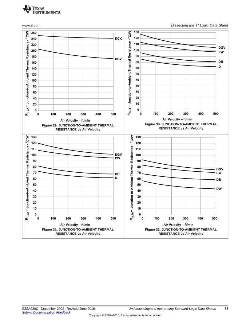
0
10
20
30
40
50
60
70
80
90
100
110
120
130
0 100 200 300 400 500
Ju
nc
tio
n-t
o-A
mb
ien
tT
he
rma
lR
es
ista
nc
e-
–
θ
RJA
C/W
°
D
DB
DGVPW
Air Velocity – ft/min Air Velocity – ft/min
Ju
nc
tio
n-t
o-A
mb
ien
tT
he
rma
lR
es
ista
nc
e-
–
θ
RJ
AC
/W°
0
10
20
30
40
50
60
70
80
90
100
110
120
130
0 100 200 300 400 500
DW
PW
DB
DGV
0
20
40
60
80
100
120
140
160
180
200
220
240
260
0 100 200 300 400 500
Ju
nc
tio
n-t
o-A
mb
ien
tT
he
rma
lR
es
ista
nc
e-°C
/W
–
–
θ
RJA
DCK
Air Velocity – ft/min
DBV
0
10
20
30
40
50
60
70
80
90
100
110
120
130
0 100 200 300 400 500
Ju
ncti
on
-to
-Am
bie
nt
Th
erm
alR
esis
tan
ce
-–
θ
RJA
C/W
°
D
DB
DGV
PW
Air Velocity – ft/min
www.ti.com Dissecting the TI Logic Data Sheet
33SZZA036C–December 2002–Revised June 2016Submit Documentation Feedback
Copyright © 2002–2016, Texas Instruments Incorporated
Understanding and Interpreting Standard-Logic Data Sheets
Figure 29. JUNCTION-TO-AMBIENT THERMALRESISTANCE vs Air Velocity
Figure 30. JUNCTION-TO-AMBIENT THERMALRESISTANCE vs Air Velocity
Figure 31. JUNCTION-TO-AMBIENT THERMALRESISTANCE vs Air Velocity
Figure 32. JUNCTION-TO-AMBIENT THERMALRESISTANCE vs Air Velocity
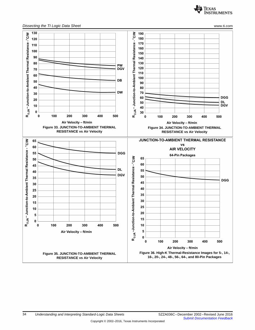
Air Velocity – ft/min
JUNCTION-TO-AMBIENT THERMAL RESISTANCE
vs
AIR VELOCITY
–J
un
cti
on
-to
-Am
bie
nt
Th
erm
alR
es
ista
nc
e-
θ
RJA
C/W
°
64-Pin Packages
0
5
10
15
20
25
30
35
40
45
50
55
60
65
0 100 200 300 400 500
DGG
0
5
10
15
20
25
30
35
40
45
50
55
60
65
0 100 200 300 400 500
–Ju
ncti
on
-to
-Am
bie
nt
Th
erm
alR
esis
tan
ce
-
θ
RJA
C/W
°
DGG
DL
Air Velocity – ft/min
DGV
Air Velocity – ft/min
–Ju
ncti
on
-to
-Am
bie
nt
Th
erm
alR
esis
tan
ce
-
θ
RJ
AC
/W°
30
40
50
60
70
80
90
100
110
120
130
140
150
160
170
180
190
0 100 200 300 400 500
DGG
DGVDL
Air Velocity – ft/min
–Ju
ncti
on
-to
-Am
bie
nt
Th
erm
alR
esis
tan
ce
-
θ
RJ
AC
/W°
0
10
20
30
40
50
60
70
80
90
100
110
120
130
0 100 200 300 400 500
DW
DB
DGVPW
Dissecting the TI Logic Data Sheet www.ti.com
34 SZZA036C–December 2002–Revised June 2016Submit Documentation Feedback
Copyright © 2002–2016, Texas Instruments Incorporated
Understanding and Interpreting Standard-Logic Data Sheets
Figure 33. JUNCTION-TO-AMBIENT THERMALRESISTANCE vs Air Velocity
Figure 34. JUNCTION-TO-AMBIENT THERMALRESISTANCE vs Air Velocity
Figure 35. JUNCTION-TO-AMBIENT THERMALRESISTANCE vs Air Velocity
Figure 36. High-K Thermal-Resistance Images for 5-, 14-,16-, 20-, 24-, 48-, 56-, 64-, and 80-Pin Packages
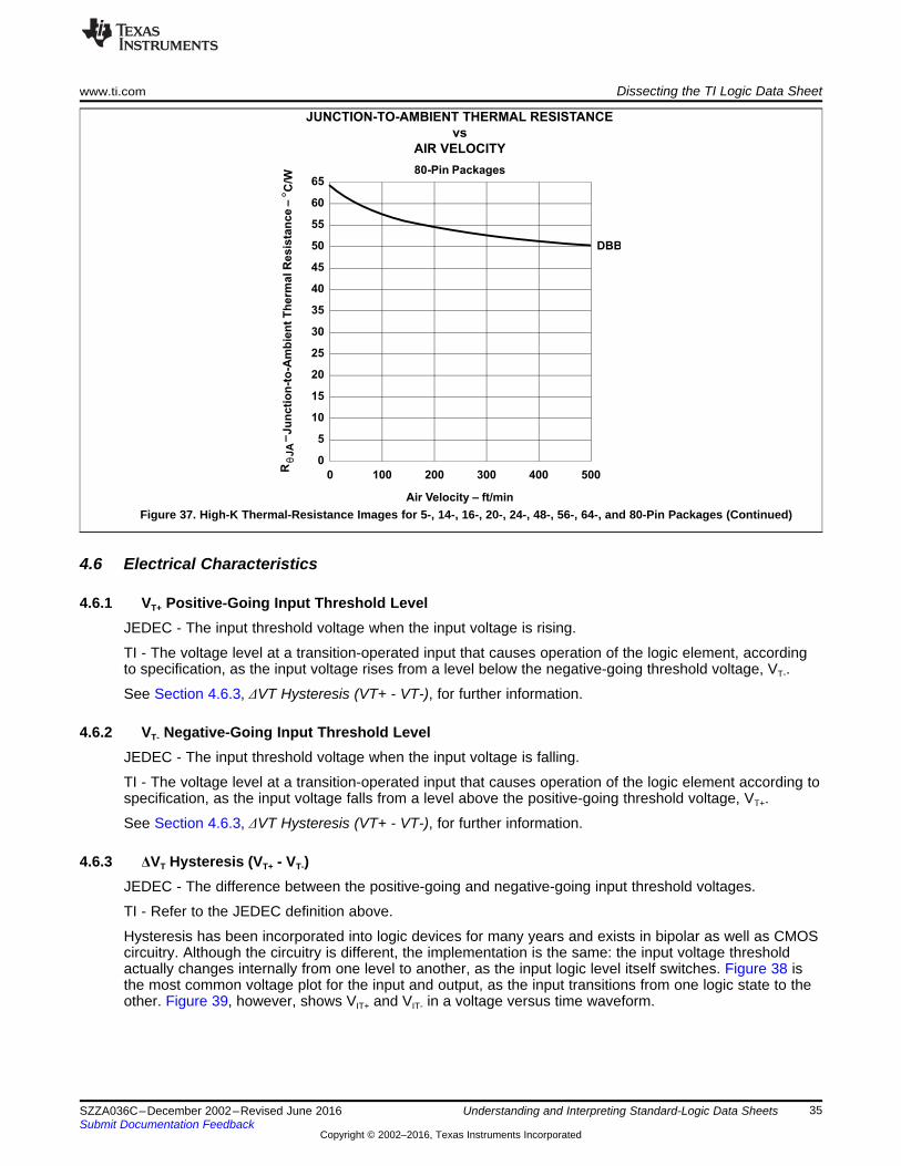
Air Velocity – ft/min
JUNCTION-TO-AMBIENT THERMAL RESISTANCE
vs
AIR VELOCITY
–Ju
ncti
on
-to
-Am
bie
nt
Th
erm
alR
esis
tan
ce
–
θ
RJA
C/W
°
80-Pin Packages
0
5
10
15
20
25
30
35
40
45
50
55
60
65
0 100 200 300 400 500
DBB
www.ti.com Dissecting the TI Logic Data Sheet
35SZZA036C–December 2002–Revised June 2016Submit Documentation Feedback
Copyright © 2002–2016, Texas Instruments Incorporated
Understanding and Interpreting Standard-Logic Data Sheets
Figure 37. High-K Thermal-Resistance Images for 5-, 14-, 16-, 20-, 24-, 48-, 56-, 64-, and 80-Pin Packages (Continued)
4.6 Electrical Characteristics
4.6.1 VT+ Positive-Going Input Threshold LevelJEDEC - The input threshold voltage when the input voltage is rising.
TI - The voltage level at a transition-operated input that causes operation of the logic element, accordingto specification, as the input voltage rises from a level below the negative-going threshold voltage, VT-.
See Section 4.6.3, ΔVT Hysteresis (VT+ - VT-), for further information.
4.6.2 VT- Negative-Going Input Threshold LevelJEDEC - The input threshold voltage when the input voltage is falling.
TI - The voltage level at a transition-operated input that causes operation of the logic element according tospecification, as the input voltage falls from a level above the positive-going threshold voltage, VT+.
See Section 4.6.3, ΔVT Hysteresis (VT+ - VT-), for further information.
4.6.3 ΔVT Hysteresis (VT+ - VT-)JEDEC - The difference between the positive-going and negative-going input threshold voltages.
TI - Refer to the JEDEC definition above.
Hysteresis has been incorporated into logic devices for many years and exists in bipolar as well as CMOScircuitry. Although the circuitry is different, the implementation is the same: the input voltage thresholdactually changes internally from one level to another, as the input logic level itself switches. Figure 38 isthe most common voltage plot for the input and output, as the input transitions from one logic state to theother. Figure 39, however, shows VIT+ and VIT- in a voltage versus time waveform.
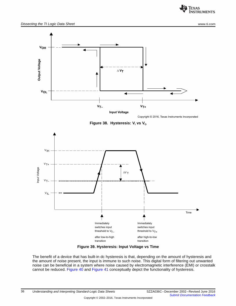
Time
Immediately
switches input
threshold to VT–
after low-to-high
transition
Immediately
switches input
threshold to VT+
after high-to-low
transition
VIH
VT+
VT–
VIL
InputV
oltage
∆V T
Ou
tpu
tV
olt
ag
e
VOH
VOL
VT– VT+
∆ VT
Input Voltage
Copyright © 2016, Texas Instruments Incorporated
Dissecting the TI Logic Data Sheet www.ti.com
36 SZZA036C–December 2002–Revised June 2016Submit Documentation Feedback
Copyright © 2002–2016, Texas Instruments Incorporated
Understanding and Interpreting Standard-Logic Data Sheets
Figure 38. Hysteresis: VI vs VO
Figure 39. Hysteresis: Input Voltage vs Time
The benefit of a device that has built-in dc hysteresis is that, depending on the amount of hysteresis andthe amount of noise present, the input is immune to such noise. This digital form of filtering out unwantednoise can be beneficial in a system where noise caused by electromagnetic interference (EMI) or crosstalkcannot be reduced. Figure 40 and Figure 41 conceptually depict the functionality of hysteresis.
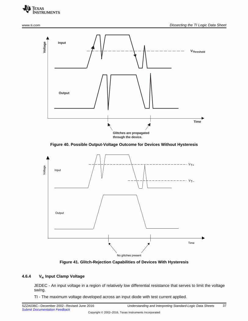
Voltage
Input
Output
Time
VT+
VT–
No glitches present
Vo
ltag
e Input
Output
VThreshold
Time
Glitches are propagatedthrough the device.
www.ti.com Dissecting the TI Logic Data Sheet
37SZZA036C–December 2002–Revised June 2016Submit Documentation Feedback
Copyright © 2002–2016, Texas Instruments Incorporated
Understanding and Interpreting Standard-Logic Data Sheets
Figure 40. Possible Output-Voltage Outcome for Devices Without Hysteresis
Figure 41. Glitch-Rejection Capabilities of Devices With Hysteresis
4.6.4 VIK Input Clamp Voltage
JEDEC - An input voltage in a region of relatively low differential resistance that serves to limit the voltageswing.
TI - The maximum voltage developed across an input diode with test current applied.
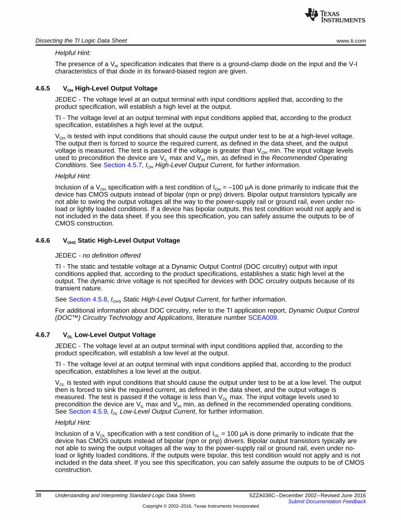
Dissecting the TI Logic Data Sheet www.ti.com
38 SZZA036C–December 2002–Revised June 2016Submit Documentation Feedback
Copyright © 2002–2016, Texas Instruments Incorporated
Understanding and Interpreting Standard-Logic Data Sheets
Helpful Hint:
The presence of a VIK specification indicates that there is a ground-clamp diode on the input and the V-Icharacteristics of that diode in its forward-biased region are given.
4.6.5 VOH High-Level Output VoltageJEDEC - The voltage level at an output terminal with input conditions applied that, according to theproduct specification, will establish a high level at the output.
TI - The voltage level at an output terminal with input conditions applied that, according to the productspecification, establishes a high level at the output.
VOH is tested with input conditions that should cause the output under test to be at a high-level voltage.The output then is forced to source the required current, as defined in the data sheet, and the outputvoltage is measured. The test is passed if the voltage is greater than VOH min. The input voltage levelsused to precondition the device are VIL max and VIH min, as defined in the Recommended OperatingConditions. See Section 4.5.7, IOH High-Level Output Current, for further information.
Helpful Hint:
Inclusion of a VOH specification with a test condition of IOH = –100 µA is done primarily to indicate that thedevice has CMOS outputs instead of bipolar (npn or pnp) drivers. Bipolar output transistors typically arenot able to swing the output voltages all the way to the power-supply rail or ground rail, even under no-load or lightly loaded conditions. If a device has bipolar outputs, this test condition would not apply and isnot included in the data sheet. If you see this specification, you can safely assume the outputs to be ofCMOS construction.
4.6.6 VOHS Static High-Level Output Voltage
JEDEC - no definition offered
TI - The static and testable voltage at a Dynamic Output Control (DOC circuitry) output with inputconditions applied that, according to the product specifications, establishes a static high level at theoutput. The dynamic drive voltage is not specified for devices with DOC circuitry outputs because of itstransient nature.
See Section 4.5.8, IOHS Static High-Level Output Current, for further information.
For additional information about DOC circuitry, refer to the TI application report, Dynamic Output Control(DOC™) Circuitry Technology and Applications, literature number SCEA009.
4.6.7 VOL Low-Level Output VoltageJEDEC - The voltage level at an output terminal with input conditions applied that, according to theproduct specification, will establish a low level at the output.
TI - The voltage level at an output terminal with input conditions applied that, according to the productspecification, establishes a low level at the output.
VOL is tested with input conditions that should cause the output under test to be at a low level. The outputthen is forced to sink the required current, as defined in the data sheet, and the output voltage ismeasured. The test is passed if the voltage is less than VOL max. The input voltage levels used toprecondition the device are VIL max and VIH min, as defined in the recommended operating conditions.See Section 4.5.9, IOL Low-Level Output Current, for further information.
Helpful Hint:
Inclusion of a VOL specification with a test condition of IOL = 100 µA is done primarily to indicate that thedevice has CMOS outputs instead of bipolar (npn or pnp) drivers. Bipolar output transistors typically arenot able to swing the output voltages all the way to the power-supply rail or ground rail, even under no-load or lightly loaded conditions. If the outputs were bipolar, this test condition would not apply and is notincluded in the data sheet. If you see this specification, you can safely assume the outputs to be of CMOSconstruction.
www.ti.com Dissecting the TI Logic Data Sheet
39SZZA036C–December 2002–Revised June 2016Submit Documentation Feedback
Copyright © 2002–2016, Texas Instruments Incorporated
Understanding and Interpreting Standard-Logic Data Sheets
4.6.8 VOLS Static Low-Level Output Voltage
JEDEC - no definition offered
TI - The static and testable voltage at a Dynamic Output Control (DOC circuitry) output with inputconditions applied that, according to the product specifications, establishes a static low level at the output.The dynamic drive voltage is not specified for devices with DOC circuitry outputs because of its transientnature.
See Section 4.5.10, IOLS Static Low-level Output Current, for further information.
For additional information about DOC circuitry, refer to the TI application report, Dynamic Output Control(DOC™) Circuitry Technology and Applications, literature number SCEA009.
4.6.9 ron On-State ResistanceJEDEC - The resistance between specified terminals with input conditions applied that, according to theproduct specification, will establish minimum resistance (the on-state) between those terminals.
TI - The resistance measured across the channel drain and source (or input and output) of a bus-switchdevice.
4.6.10 Peak On-State ResistanceTI - The highest resistance measured across the drain and source channels of switch across the validinput range of operation.
4.6.11 Delta On-State ResistanceTI -The difference between the on-state resistance between any 2 channels of the switch.
4.6.12 II Input CurrentJEDEC - The current at the input terminals.
TI - The current into an input (current into a terminal is given as a positive value).
Helpful Hint:
CMOS inputs sink or source only minute amounts of current (commonly called leakage current) becauseof the behavior of standard CMOS technology, which is voltage controlled instead of current controlled. Asa result, this parameter always should have a maximum specification no greater than a few tens of microamperes. For most bipolar inputs, which are current controlled instead of voltage controlled, a largeamount of current is normal (a few milliamperes). In fact, a good method to determine if a device has aCMOS input is to examine its maximum input current specification: if this current is approximately thevalue of leakage current, typically, this means that it is a CMOS input.
Helpful Hint:
For the data signals of a device without bus-hold, the II specification includes both input and outputleakage currents at the I/O pin. For devices that have bus-hold on the data signals, the II specificationshould apply only to the control inputs because the bus-hold output supplies enough current to overcomeany internal input leakage.
An exception to this is an II specification for an overvoltage-tolerant bus-hold input with a test condition ofVI >> VCC. This is used to indicate that the overvoltage-tolerant bus-hold output has a Schottky blockingdiode in series with the output p-channel pullup transistor to VCC, which prevents current from flowing fromthe output back into the VCC supply. See II(hold) and Ioff for more information.
Dissecting the TI Logic Data Sheet www.ti.com
40 SZZA036C–December 2002–Revised June 2016Submit Documentation Feedback
Copyright © 2002–2016, Texas Instruments Incorporated
Understanding and Interpreting Standard-Logic Data Sheets
4.6.13 IIH High-Level Input CurrentJEDEC - The current into an input terminal when a specified high-level voltage is applied to that input.
TI - The current into an input when a high-level voltage is applied to that input.
Helpful Hint:
IIH and IIL typically are found only on devices with bipolar inputs that usually require a significantly differentamount of pulldown current on the input to provide a logic low, rather than pullup current to provide a logichigh. CMOS inputs usually have only leakage currents at the inputs and use the II parameter, but aremeasured at both low- and high-bias conditions.
4.6.14 IIL Low-Level Input CurrentJEDEC - The current into an input terminal when a specified low-level voltage is applied to that input.
TI - The current out of an input when a low-level voltage is applied to that input.
Helpful Hint:
IIH and IIL typically are found only on devices with bipolar inputs that usually require a significantly differentamount of pulldown current on the input to provide a logic low, rather than pullup current to provide a logichigh. CMOS inputs usually have only leakage currents at the inputs and use the II parameter.
4.6.15 II(hold) Input Hold CurrentJEDEC - no definition offered
TI - The input current that holds the input at the previous state when the driving device goes to the high-impedance state.
For additional information about the bus-hold feature, refer to the TI application report, Bus-Hold Circuit,literature number SCLA015.
Older technologies, such as ABT, LVT, LVC and ALVC (on devices that have the H option), specify thisparameter. This parameter is measured with the minimum VCC and an input bias voltage that is at VIH minand VIL max of the particular input threshold. For example, the ALVC family has a specified VIL max of 0.7V for a VCC ranging from 2.3 V to 2.7 V, whereas its VIH min is 1.7 V for the same supply voltage. Within aVCC range of 2.7 V to 3.6 V, the input threshold for the ALVC family is VIH min = 2 V and VIL max = 0.8 V.Therefore, with VCC = 2.3 V, II(hold) is measured with the input voltage set to 0.7 V and 1.7 V. With a VCC =2.7 V (minimum VCC of 2.3 V to 2.7 V), II(hold) is measured with the input voltage set to 0.8 V and 2 V. Thisspecification explicitly states the minimum amount of current the input structure sources or sinks, withinput voltages set to the minimum threshold requirements of the device.
Another parameter that may be included with this II(hold) specification is the maximum current the devicecan sink or source as the input transitions from one logic state to another. This maximum current is theminimum amount of drive capability that must be provided by the driver that is connected to this bus-holdinput to switch the input stage to the other logic state. In newer technologies such as AVC, the parametersIBHH, IBHL, IBHHO, and IBHLO have been defined with their own separate specifications, but are identical innature to those that are lumped with the II(hold) parameter. Figure 42 is a representation of these bus-holdcurrent measurements.
Helpful Hint:
The II(hold) specification is not used in recent data sheets; instead, IBHH, IBHL, IBHHO, and IBHLO are used.
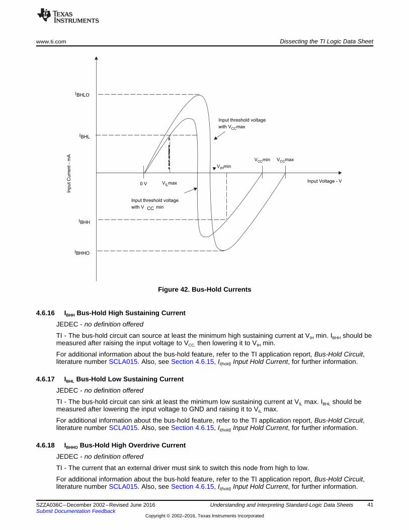
InputC
urr
ent-
mA
IBHLO
IBHL
IBHH
IBHHO
V minIH
V minCC V maxCC
Input Voltage - V
Input threshold voltage
with VCCmax
V maxIL0 V
Input threshold voltage
with V CC min
www.ti.com Dissecting the TI Logic Data Sheet
41SZZA036C–December 2002–Revised June 2016Submit Documentation Feedback
Copyright © 2002–2016, Texas Instruments Incorporated
Understanding and Interpreting Standard-Logic Data Sheets
Figure 42. Bus-Hold Currents
4.6.16 IBHH Bus-Hold High Sustaining CurrentJEDEC - no definition offered
TI - The bus-hold circuit can source at least the minimum high sustaining current at VIH min. IBHH should bemeasured after raising the input voltage to VCC, then lowering it to VIH min.
For additional information about the bus-hold feature, refer to the TI application report, Bus-Hold Circuit,literature number SCLA015. Also, see Section 4.6.15, II(hold) Input Hold Current, for further information.
4.6.17 IBHL Bus-Hold Low Sustaining CurrentJEDEC - no definition offered
TI - The bus-hold circuit can sink at least the minimum low sustaining current at VIL max. IBHL should bemeasured after lowering the input voltage to GND and raising it to VIL max.
For additional information about the bus-hold feature, refer to the TI application report, Bus-Hold Circuit,literature number SCLA015. Also, see Section 4.6.15, II(hold) Input Hold Current, for further information.
4.6.18 IBHHO Bus-Hold High Overdrive CurrentJEDEC - no definition offered
TI - The current that an external driver must sink to switch this node from high to low.
For additional information about the bus-hold feature, refer to the TI application report, Bus-Hold Circuit,literature number SCLA015. Also, see Section 4.6.15, II(hold) Input Hold Current, for further information.
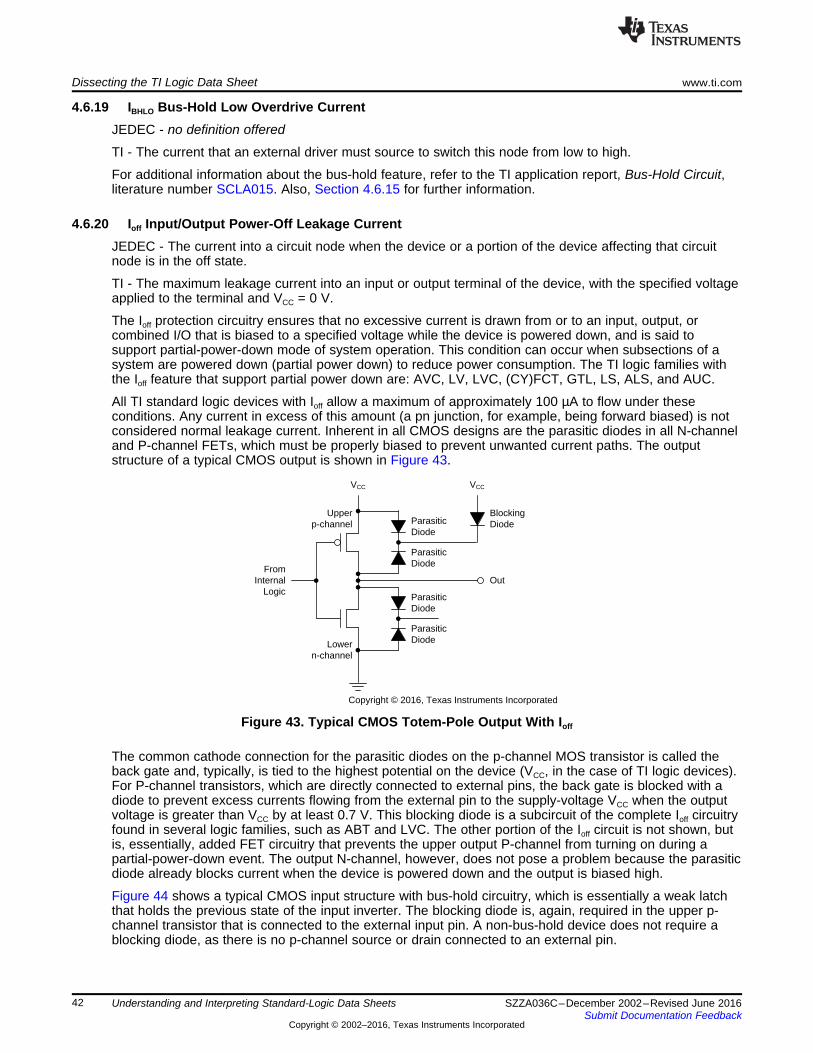
VCC VCC
BlockingDiode
Out
Lowern-channel
ParasiticDiode
ParasiticDiode
ParasiticDiode
ParasiticDiode
Upperp-channel
FromInternal
Logic
Copyright © 2016, Texas Instruments Incorporated
Dissecting the TI Logic Data Sheet www.ti.com
42 SZZA036C–December 2002–Revised June 2016Submit Documentation Feedback
Copyright © 2002–2016, Texas Instruments Incorporated
Understanding and Interpreting Standard-Logic Data Sheets
4.6.19 IBHLO Bus-Hold Low Overdrive CurrentJEDEC - no definition offered
TI - The current that an external driver must source to switch this node from low to high.
For additional information about the bus-hold feature, refer to the TI application report, Bus-Hold Circuit,literature number SCLA015. Also, Section 4.6.15 for further information.
4.6.20 Ioff Input/Output Power-Off Leakage CurrentJEDEC - The current into a circuit node when the device or a portion of the device affecting that circuitnode is in the off state.
TI - The maximum leakage current into an input or output terminal of the device, with the specified voltageapplied to the terminal and VCC = 0 V.
The Ioff protection circuitry ensures that no excessive current is drawn from or to an input, output, orcombined I/O that is biased to a specified voltage while the device is powered down, and is said tosupport partial-power-down mode of system operation. This condition can occur when subsections of asystem are powered down (partial power down) to reduce power consumption. The TI logic families withthe Ioff feature that support partial power down are: AVC, LV, LVC, (CY)FCT, GTL, LS, ALS, and AUC.
All TI standard logic devices with Ioff allow a maximum of approximately 100 µA to flow under theseconditions. Any current in excess of this amount (a pn junction, for example, being forward biased) is notconsidered normal leakage current. Inherent in all CMOS designs are the parasitic diodes in all N-channeland P-channel FETs, which must be properly biased to prevent unwanted current paths. The outputstructure of a typical CMOS output is shown in Figure 43.
Figure 43. Typical CMOS Totem-Pole Output With Ioff
The common cathode connection for the parasitic diodes on the p-channel MOS transistor is called theback gate and, typically, is tied to the highest potential on the device (VCC, in the case of TI logic devices).For P-channel transistors, which are directly connected to external pins, the back gate is blocked with adiode to prevent excess currents flowing from the external pin to the supply-voltage VCC when the outputvoltage is greater than VCC by at least 0.7 V. This blocking diode is a subcircuit of the complete Ioff circuitryfound in several logic families, such as ABT and LVC. The other portion of the Ioff circuit is not shown, butis, essentially, added FET circuitry that prevents the upper output P-channel from turning on during apartial-power-down event. The output N-channel, however, does not pose a problem because the parasiticdiode already blocks current when the device is powered down and the output is biased high.
Figure 44 shows a typical CMOS input structure with bus-hold circuitry, which is essentially a weak latchthat holds the previous state of the input inverter. The blocking diode is, again, required in the upper p-channel transistor that is connected to the external input pin. A non-bus-hold device does not require ablocking diode, as there is no p-channel source or drain connected to an external pin.
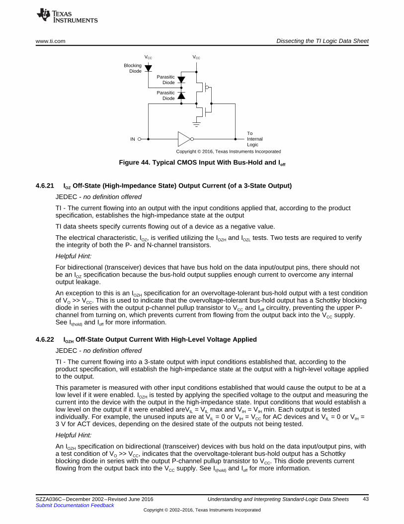
INToInternalLogic
VCC
ParasiticDiode
ParasiticDiode
VCC
BlockingDiode
Copyright © 2016, Texas Instruments Incorporated
www.ti.com Dissecting the TI Logic Data Sheet
43SZZA036C–December 2002–Revised June 2016Submit Documentation Feedback
Copyright © 2002–2016, Texas Instruments Incorporated
Understanding and Interpreting Standard-Logic Data Sheets
Figure 44. Typical CMOS Input With Bus-Hold and Ioff
4.6.21 IOZ Off-State (High-Impedance State) Output Current (of a 3-State Output)JEDEC - no definition offered
TI - The current flowing into an output with the input conditions applied that, according to the productspecification, establishes the high-impedance state at the output
TI data sheets specify currents flowing out of a device as a negative value.
The electrical characteristic, IOZ, is verified utilizing the IOZH and IOZL tests. Two tests are required to verifythe integrity of both the P- and N-channel transistors.
Helpful Hint:
For bidirectional (transceiver) devices that have bus hold on the data input/output pins, there should notbe an IOZ specification because the bus-hold output supplies enough current to overcome any internaloutput leakage.
An exception to this is an IOZH specification for an overvoltage-tolerant bus-hold output with a test conditionof VO >> VCC. This is used to indicate that the overvoltage-tolerant bus-hold output has a Schottky blockingdiode in series with the output p-channel pullup transistor to VCC and Ioff circuitry, preventing the upper P-channel from turning on, which prevents current from flowing from the output back into the VCC supply.See II(hold) and Ioff for more information.
4.6.22 IOZH Off-State Output Current With High-Level Voltage AppliedJEDEC - no definition offered
TI - The current flowing into a 3-state output with input conditions established that, according to theproduct specification, will establish the high-impedance state at the output with a high-level voltage appliedto the output.
This parameter is measured with other input conditions established that would cause the output to be at alow level if it were enabled. IOZH is tested by applying the specified voltage to the output and measuring thecurrent into the device with the output in the high-impedance state. Input conditions that would establish alow level on the output if it were enabled areVIL = VIL max and VIH = VIH min. Each output is testedindividually. For example, the unused inputs are at VIL = 0 or VIH = VCC for AC devices and VIL = 0 or VIH =3 V for ACT devices, depending on the desired state of the outputs not being tested.
Helpful Hint:
An IOZH specification on bidirectional (transceiver) devices with bus hold on the data input/output pins, witha test condition of VO >> VCC, indicates that the overvoltage-tolerant bus-hold output has a Schottkyblocking diode in series with the output P-channel pullup transistor to VCC. This diode prevents currentflowing from the output back into the VCC supply. See II(hold) and Ioff for more information.
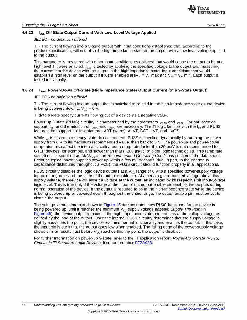
Dissecting the TI Logic Data Sheet www.ti.com
44 SZZA036C–December 2002–Revised June 2016Submit Documentation Feedback
Copyright © 2002–2016, Texas Instruments Incorporated
Understanding and Interpreting Standard-Logic Data Sheets
4.6.23 IOZL Off-State Output Current With Low-Level Voltage AppliedJEDEC - no definition offered
TI - The current flowing into a 3-state output with input conditions established that, according to theproduct specification, will establish the high-impedance state at the output, with a low-level voltage appliedto the output.
This parameter is measured with other input conditions established that would cause the output to be at ahigh level if it were enabled. IOZL is tested by applying the specified voltage to the output and measuringthe current into the device with the output in the high-impedance state. Input conditions that wouldestablish a high level on the output if it were enabled areVIL = VIL max and VIH = VIH min. Each output istested individually.
4.6.24 IOZPD Power-Down Off-State (High-Impedance State) Output Current (of a 3-State Output)JEDEC - no definition offered
TI - The current flowing into an output that is switched to or held in the high-impedance state as the deviceis being powered down to VCC = 0 V.
TI data sheets specify currents flowing out of a device as a negative value.
Power-up 3-state (PU3S) circuitry is characterized by the parameters IOZPD and IOZPU. For hot-insertionsupport, Ioff, and the addition of IOZPD and IOZPU are necessary. The TI logic families with the Ioff and PU3Sfeatures that support hot insertion are: ABT (some), ALVT, BCT, LVT, and LVCZ.
While Ioff is tested in a steady-state dc environment, PU3S is checked dynamically by ramping the powersupply from 0 V to its maximum recommended value, then back to 0 V. The power-up and power-downramp rates also affect the internal circuitry, but a ramp rate faster than 20 µs/V is not recommended forGTLP devices, for example, and slower than that (~200 µs/V) for older logic technologies. This ramp ratesometimes is specified as Δt/ΔVCC in the Recommended Operating Conditions section of the data sheet.Because typical power supplies power up within a few milliseconds (due, in part, to the enormouscapacitance distributed throughout a PCB), the PU3S circuit should function properly in all applications.
PU3S circuitry disables the logic device outputs at a VCC range of 0 V to a specified power-supply voltagetrip point, regardless of the state of the output enable pin. At a certain guard-banded voltage above thissupply voltage, the device will assert a voltage at the output, as indicated by its respective bit input-voltagelogic level. This is true only if the voltage at the input of the output-enable pin enables the outputs duringnormal operation of the device. If the output is required to be in the high-impedance state while the deviceis being powered up or powered down throughout the entire range, the output-enable pin must be set todisable the output.
The voltage-versus-time plot shown in Figure 45 demonstrates how PU3S functions. As the device isbeing powered up, until it reaches the minimum VCC supply voltage (labeled Supply Trip Point inFigure 45), the device output remains in the high-impedance state and remains at the pullup voltage, asdefined by the load at the output. Once the internal PU3S circuitry determines that the supply voltage isslightly above this trip point, the device resumes normal functionality and enables the output. In this case,the input pin is such that the output goes low when enabled. The falling edge of the power-supply voltageshows similar results: just before VCC reaches this trip point, the output is disabled.
For further information on power-up 3-state, refer to the TI application report, Power-Up 3-State (PU3S)Circuits in TI Standard Logic Devices, literature number SZZA033.
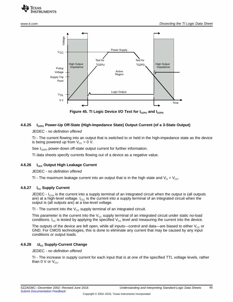
VCC
Pullup
Voltage
Supply Trip
Point
VOL
0 V
Voltage
High OutputImpedance
High OutputImpedance
Power Supply
ActiveRegion
Logic Output
Test for
IOZPU
Test for
IOZPD
Time
www.ti.com Dissecting the TI Logic Data Sheet
45SZZA036C–December 2002–Revised June 2016Submit Documentation Feedback
Copyright © 2002–2016, Texas Instruments Incorporated
Understanding and Interpreting Standard-Logic Data Sheets
Figure 45. TI Logic Device I/O Text for IOZPU and IOZPD
4.6.25 IOZPU Power-Up Off-State (High-Impedance State) Output Current (of a 3-State Output)JEDEC - no definition offered
TI - The current flowing into an output that is switched to or held in the high-impedance state as the deviceis being powered up from VCC = 0 V.
See IOZPD power-down off-state output current for further information.
TI data sheets specify currents flowing out of a device as a negative value.
4.6.26 ICEX Output High Leakage CurrentJEDEC - no definition offered
TI - The maximum leakage current into an output that is in the high state and VO = VCC.
4.6.27 ICC Supply CurrentJEDEC - ICCH is the current into a supply terminal of an integrated circuit when the output is (all outputsare) at a high-level voltage. ICCL is the current into a supply terminal of an integrated circuit when theoutput is (all outputs are) at a low-level voltage.
TI - The current into the VCC supply terminal of an integrated circuit.
This parameter is the current into the VCC supply terminal of an integrated circuit under static no-loadconditions. ICC is tested by applying the specified VCC level and measuring the current into the device.
The outputs of the device are left open, while all inputs—control and data—are biased to either VCC orGND. For CMOS technologies, this is done to eliminate any current that may be caused by any inputconditions or output loads.
4.6.28 ΔICC Supply-Current ChangeJEDEC - no definition offered
TI - The increase in supply current for each input that is at one of the specified TTL voltage levels, ratherthan 0 V or VCC.
VCC = 5 V
AC
AHC
I CC
− m
A
5
4
3
2
1
0 1 2 3 4 5
Input V oltage − V
Dissecting the TI Logic Data Sheet www.ti.com
46 SZZA036C–December 2002–Revised June 2016Submit Documentation Feedback
Copyright © 2002–2016, Texas Instruments Incorporated
Understanding and Interpreting Standard-Logic Data Sheets
If n inputs are at voltages other than 0 V or VCC, the increase in supply current will be n × ICC. The changein supply current (ICC) is tested by applying the specified VCC level, setting one input lower than VCC (forexample, VCC - 0.6 V for LVC and ALVC devices) and all other inputs the same as the ICC test, at 0 V orVCC, then measuring the current into the device (see Figure 46). The outputs of the device are open, aswell. The ΔICC specification typically is useful only on CMOS products that are designed to be operated at5 V or 3.3 V because its purpose is to provide information about the supply-current performance of theCMOS device when driven by 5-V TTL signal levels.
Figure 46. Example Typical AC and AHC ICC vs Input Voltage
Helpful Hint:
Use the ΔICC specification as a reference when driving a CMOS device input with a TTL output driver.
Helpful Hint:
The ΔICC specification also demonstrates the high currents that can occur if VIH and VIL recommendedoperating conditions are not observed.
4.6.29 Ci Input CapacitanceJEDEC - no definition offered
TI - The capacitance of an input terminal of the device.
This parameter is the internal capacitance encountered at an input of the device. The values that aregiven are not production-tested values. Normally, they are typical values given for the benefit of thedesigner. These values are established by the design, process, and package of the device.
4.6.30 Cio Input/Output CapacitanceJEDEC - no definition offered
TI - The capacitance of an input/output (I/O) terminal of the device with the input conditions applied that,according to the product specification, establishes the high-impedance state at the output.
This parameter is the internal capacitance encountered at an input/output (I/O) of the device. The valuesthat are given are not production-tested values. Normally, they are typical values given for the benefit ofthe designer. These values are established by the design, process, and package of the device.
4.6.31 Co Output CapacitanceJEDEC - no definition offered
www.ti.com Dissecting the TI Logic Data Sheet
47SZZA036C–December 2002–Revised June 2016Submit Documentation Feedback
Copyright © 2002–2016, Texas Instruments Incorporated
Understanding and Interpreting Standard-Logic Data Sheets
TI - The capacitance of an output terminal of the device with the input conditions applied that, according tothe product specification, establishes the high-impedance state at the output.
This parameter is the internal capacitance encountered at an output of the device. The values that aregiven are not production-tested values. Normally, they are typical values given for the benefit of thedesigner. These values are defined by the design, process, and package of the device.
4.7 Live-Insertion SpecificationsIn addition to the following parameters, Ioff, IOZPU, and IOZPD are specified in the live-insertion table becausethese parameters are necessary for live-insertion applications and typically are not stated in the electricalcharacteristics section of the data sheet, if already mentioned in this section.
4.7.1 ICC (BIAS VCC) BIAS VCC CurrentJEDEC - no definition offered
TI - This specification defines the maximum current at the BIAS VCC pin during the ramp up or ramp downof the VCC voltage.
4.7.2 VO Output Bias VoltageJEDEC - no definition offered
TI - This specification defines the range of voltages that will be applied to the output pin when the deviceis powered down.
4.7.3 IO Output Bias CurrentJEDEC - no definition offered
TI - This specification defines the minimum current measured at the output pin when the device ispowered down.
4.8 Timing Requirements
4.8.1 fclock Clock FrequencyJEDEC - no definition offered
TI - This specification defines the range of clock frequencies over which a bistable device can be operatedwhile maintaining stable transitions between logic levels at the outputs.
The fclock parameter is tested by driving the clock input with a predetermined number of pulses. The outputthen is checked for the correct number of output transitions corresponding to the number of input pulsesapplied. The output is loaded as defined in the data sheet specifications. Each output is individually testedand not checked simultaneously with other recommended operating conditions or propagation delays. Forcounters, shift registers, or any other devices for which the state of the final output is dependent on thecorrect operation of the previous outputs, fclock will be tested only on the final output, unless specifiedindependently in the data sheet. Full functionality testing is not performed during fclock testing or fmax testing.
Helpful Hint:
The fmax and fclock parameters are two sides of the same coin. The fclock parameter tells you, the user, howfast you can reliably switch the input to the device. The fmax parameter informs TI when to reject a devicethat fails to function below a minimum speed. If you are a device user, you should simply disregard the fmaxspecification and use the fclock specification.
Helpful Hint:
For products that are not clocked (for example, buffers and transceivers) for which you would like to knowthe maximum operating frequency, an estimate is the fclock value from a comparable clocked part. Forexample, an SN74LVC16245A maximum data frequency is conservatively similar to the SN74LVC16374maximum clock frequency. However, this is highly dependent upon load, and is a rule-of-thumb only.

Inp
ut
VIH
VIL
DataInput
Time
VT
tw
VT
Vo
ltag
e
Dissecting the TI Logic Data Sheet www.ti.com
48 SZZA036C–December 2002–Revised June 2016Submit Documentation Feedback
Copyright © 2002–2016, Texas Instruments Incorporated
Understanding and Interpreting Standard-Logic Data Sheets
4.8.2 tw Pulse Duration (Width)JEDEC - The time interval between the specified reference points on the two transitions of the pulsewaveform.
TI - The time interval between specified reference points on the leading and trailing edges of the pulsewaveform.
A minimum value is specified that is the shortest interval for which correct operation of the digital circuit isspecified (see Figure 47). Pulse duration is tested by applying a pulse to the specified input for a timeperiod equal to the minimum specified in the data sheet. The device passes if the outputs switch to theirexpected logic levels and fails if they do not. Pulse-duration times are not checked simultaneously withother inputs or other recommended operating conditions.
Figure 47. Pulse Duration
4.8.3 tsu Setup TimeJEDEC - The time interval between the application of a signal at a specified input terminal and asubsequent active transition at another specified input terminal.
TI - The time interval between the application of a signal that is maintained at a specified input terminaland a consecutive active transition at another specified input terminal.
NOTE: 1. The setup time is the time interval between two signal events and is determined by thesystem in which the digital circuit operates. A minimum value is specified that is the shortestinterval for which correct operation of the digital circuit is specified.
NOTE: 2. The setup time may have a negative value, in which case the minimum limit defines thelongest interval (between the active transition and the application of the other signal) forwhich correct operation of the digital circuit is specified.
Setup time is tested by switching an input to a fixed logic level at a specified time before the transition ofthe other input (see Figure 48). The device passes if the outputs switch to their expected logic levels andfails if they do not. Setup times are not checked simultaneously with other inputs or other recommendedoperating conditions. For additional information about setup time, refer to the TI application report,Metastable Response in 5-V Logic Circuits, literature number SDYA006.
Inp
ut V
olt
age
Inp
ut V
olt
age
VIH
VIL
VIH
VIL
TimingInput
DataInput
Time
Time
VT
VT VT
tsu th
www.ti.com Dissecting the TI Logic Data Sheet
49SZZA036C–December 2002–Revised June 2016Submit Documentation Feedback
Copyright © 2002–2016, Texas Instruments Incorporated
Understanding and Interpreting Standard-Logic Data Sheets
4.8.4 th Hold TimeJEDEC - The time interval during which a signal is retained at a specified input terminal after an activetransition occurs at another specified input terminal.
TI - The time interval during which a signal is retained at a specified input after an active transition occursat another specified input.
NOTE: 1. The hold time is the actual time interval between two signal events and is determined bythe system in which the digital signal operates. A minimum value is specified that is theshortest interval for which correct operation of the digital circuit is to be expected.
NOTE: 2. The hold time may have a negative value, in which case, the minimum limit defines thelongest interval (between the release of the signal and the active transition) for which correctoperation of the digital circuit is to be expected.
Hold time is tested by holding an input at a fixed logic level for the specified time after the transition of theother input (see Figure 48). The device passes if the outputs switch to their expected logic levels and failsif they do not. Hold times are not checked simultaneously with other inputs or other recommendedoperating conditions. For additional information about hold time, refer to the TI application report;Metastable Response in 5-V Logic Circuits, literature number SDYA006.
Figure 48. Setup and Hold Times
Dissecting the TI Logic Data Sheet www.ti.com
50 SZZA036C–December 2002–Revised June 2016Submit Documentation Feedback
Copyright © 2002–2016, Texas Instruments Incorporated
Understanding and Interpreting Standard-Logic Data Sheets
4.9 Switching Characteristics
4.9.1 fmax Maximum Clock FrequencyJEDEC - The highest frequency at which a clock input of an integrated circuit can be driven, whilemaintaining proper operation.
TI - The highest rate at which the clock input of a bistable circuit can be driven through its requiredsequence, while maintaining stable transitions of logic level at the output with input conditions establishedthat should cause changes of output logic level in accordance with the specification.
The fmax value is the value of the upper limit of the fclock specification, and is specified in the data sheet as aminimum limit. The circuit is specified to operate up to the minimum frequency value. See fclock foradditional fmax testing information. Due to test-machine capability limitations, it may be necessary to testfmax or minimum recommended operating conditions (that is, pulse duration, setup time, hold time) inaccordance with the following paragraph.
The fmax parameter may be tested in either of two ways. One method is to test simultaneously theresponses to the symmetrical clock-high and clock-low pulse durations that correspond to the period of thespecified minimum value of fmax. The second method is to test individually the responses to the minimumclock-high and clock-low pulse durations under specified load conditions. A pulse generator is used topropagate a signal through the device to verify device operation with the minimum pulse duration. Whenclock-high and clock-low pulse durations are equal to or less than the corresponding fmax pulse duration,fmax testing suffices for testing clock-high and clock-low pulse durations.
Helpful Hint:
The fmax and fclock parameters are two sides of the same coin. The fclock parameter tells you, the user, howfast you can reliably switch the input to the device. The fmax parameter informs TI when to reject a devicethat fails to function below a minimum speed. If you are a device user, you should simply disregard the fmaxspecification and use the fclock specification.
Helpful Hint:
For products that are not clocked (for example, buffers and transceivers) for which you would like to knowthe maximum operating frequency, an estimate is the fclock value from a comparable clocked part. Forexample, an SN74LVC162451A maximum data frequency is conservatively similar to the SN74LVC16374maximum clock frequency. However, this is highly dependent upon load and is a rule-of-thumb only.
4.9.2 tpd Propagation Delay TimeJEDEC - The time interval between specified reference points on the input and output voltage waveformswith the output changing from one defined level (high or low) to the other defined level.
TI - The time between the specified reference points on the input and output voltage waveforms, with theoutput changing from one defined level (high or low) to the other defined level (tpd = tPHL or tPLH).
A common misconception about logic devices is that the maximum data-signaling rate (or maximumfrequency, as it is commonly misnamed) is equal to the inverse of the propagation delay. The maximumdata rate on buffers is dependent on several factors, such as propagation delay matching, input sensitivity,and output edge rates. A device can have a high maximum signaling rate if the propagation delays fromlow-to-high and high-to-low are matched, the input is fast enough to respond to the fast data rate, and theoutput edge rate does not interfere with the low and high-level steady states. Clocked devices behave inthe same manner, but now the set-up and hold times must be taken into account.
Helpful Hint:
The maximum value of tPD simply is the worst case of tPHL or tPLH.
Helpful Hint:
Bus switch devices such as CBT and CBTLV typically are specified with a maximum limit of 0.25 ns. Thislimit is not a measured value, but is derived from the calculated RC time constant of the typical on-stateresistance of the switch and the specified load capacitance, when driven by an ideal voltage source (zerooutput impedance).
www.ti.com Dissecting the TI Logic Data Sheet
51SZZA036C–December 2002–Revised June 2016Submit Documentation Feedback
Copyright © 2002–2016, Texas Instruments Incorporated
Understanding and Interpreting Standard-Logic Data Sheets
4.9.3 tPHL Propagation Delay Time, High-Level to Low-Level OutputJEDEC - The time interval between specified reference points on the input and output voltage waveformswith the output changing from the defined high level to the defined low level.
TI - The time between the specified reference points on the input and output voltage waveforms, with theoutput changing from the defined high level to the defined low level.
Propagation delay time, tPHL, is tested by causing a transition on the specified input that causes thedesignated output to switch from a high logic level to a low logic level. For example, the transition appliedis 0 V to VCC or VCC to 0 V for AC devices and 0 V to 3 V or 3 V to 0 for ACT devices. Trip points used forthe timing measurements and output loads used during testing are defined in the individual data sheets inthe Parameter Measurement Information section, typically found after the Switching Characteristics (overrecommended ranges of supply and operating free-air temperature) table. Propagation delay time, tPHL, isnot checked simultaneously with other outputs or with other recommended operating conditions. The timebetween the specified reference point on the input voltage waveform and the specified reference point onthe output voltage waveform is measured.
4.9.4 tPLH Propagation Delay Time, Low-Level to High-Level OutputJEDEC - The time interval between specified reference points on the input and output voltage waveformswith the specified output changing from the defined low level to the defined high level.
TI - The time between the specified reference points on the input and output voltage waveforms, with theoutput changing from the defined low level to the defined high level.
Propagation delay time, tPLH, is tested by causing a transition on the specified input that causes thedesignated output to switch from a low logic level to a high logic level. For example, the transition appliedis 0 V to VCC or VCC to 0 V for AC devices and 0 V to 3 V or 3 V to 0 for ACT devices. Trip points used forthe timing measurements and output loads used during testing are defined in the individual data sheets inthe Parameter Measurement Information section, typically found after the Switching Characteristics (overrecommended ranges of supply and operating free-air temperature) table. Propagation delay time, tPLH, isnot checked simultaneously with other outputs or with other recommended operating conditions. The timebetween the specified reference point on the input voltage waveform and the specified reference point onthe output voltage waveform is measured.
4.9.5 ten Enable Time (of a 3-State or Open-Collector Output)JEDEC - The propagation time between specified reference points on the input and output voltagewaveforms with the output changing from a high-impedance (off) state to either of the defined active levels(high or low).
TI - The propagation time between the specified reference points on the input and output voltagewaveforms, with the output changing from the high-impedance (off) state to either of the defined activelevels (high or low).
NOTE: Open-collector outputs change only if they are responding to data that would cause theoutput to go low, so ten = tPHL.
4.9.6 tPZH Enable Time (of a 3-State Output) to High LevelJEDEC - The propagation time between specified reference points on the input and output voltagewaveforms with the output changing from a high-impedance (off) state to the defined high level.
TI - The time interval between the specified reference points on the input and output voltage waveforms,with the 3-state output changing from the high-impedance (off) state to the defined high level.
This parameter is the propagation delay time between the specified reference point on the input voltagewaveform and the specified reference point on the output voltage waveform, with the 3-state outputchanging from the high-impedance (off) state to the defined high level. Output enable time, tPZH, is testedby generating a transition on the specified input that will cause the designated output to switch from thehigh-impedance state to a high logic level. Trip points used for the timing measurements and output loadsused during testing are defined in the individual data sheets in the Parameter Measurement Information
Dissecting the TI Logic Data Sheet www.ti.com
52 SZZA036C–December 2002–Revised June 2016Submit Documentation Feedback
Copyright © 2002–2016, Texas Instruments Incorporated
Understanding and Interpreting Standard-Logic Data Sheets
section, typically found after the Switching Characteristics (over recommended ranges of supply andoperating free-air temperature) table. Output enable time, tPZH, is not checked simultaneously with otheroutputs or with other recommended operating conditions. Outputs not being tested should be set to acondition that minimizes switching currents. The tested output load includes a pulldown resistor to obtain avalid logic-low level when the output is in the high-impedance state.
4.9.7 tPZL Enable Time (of a 3-State Output) to Low LevelJEDEC - The propagation time between specified reference points on the input and output voltagewaveforms with the output changing from a high-impedance (off) state to the defined low level.
TI - The time interval between the specified reference points on the input and output voltage waveforms,with the 3-state output changing from the high-impedance (off) state to the defined low level.
This parameter is the propagation delay time between the specified reference point on the input voltagewaveform and the specified reference point on the output voltage waveform, with the 3-state outputchanging from the high-impedance (off) state to the defined low level. Output enable time, tPZL, is tested bygenerating a transition on the specified input that will cause the designated output to switch from the high-impedance state to a low logic level. Trip points used for the timing measurements and output loads usedduring testing are defined in the individual data sheets in the Parameter Measurement Information section,typically found after the Switching Characteristics (over recommended ranges of supply and operatingfree-air temperature) table. Output enable time, tPZL, is not checked simultaneously with other outputs orwith other recommended operating conditions. Outputs not being tested should be set to a condition thatminimizes switching currents. The tested output load includes a pullup resistor to obtain a valid logic-highlevel when the output is in the high-impedance state.
4.9.8 tdis Disable Time (of a 3-State or Open-Collector Output)JEDEC - no definition offered
TI - The propagation time between the specified reference points on the input and output voltagewaveforms, with the output changing from either of the defined active levels (high or low) to the high-impedance (off) state.
NOTE: For 3-state outputs, tdis = tPHZ or tPLZ. Open-collector outputs change only if they are low at thetime of disabling, so tdis = tPLH.
4.9.9 tPHZ Disable Time (of a 3-State Output) From High LevelJEDEC - The propagation time between specified reference points on the input and output voltagewaveforms with the output changing from the defined high level to a high-impedance (off) state.
TI - The time interval between the specified reference points on the input and the output voltagewaveforms, with the 3-state output changing from the defined high level to the high-impedance (off) state.
4.9.10 tPLZ Disable Time (of a 3-State Output) From Low LevelJEDEC - The propagation time between specified reference points on the input and output voltagewaveforms with the output changing from the defined low level to a high-impedance (off) state.
TI - The time interval between the specified reference points on the input and the output voltagewaveforms, with the 3-state output changing from the defined low level to the high-impedance (off) state.
4.9.11 tf Fall TimeJEDEC - The time interval between one reference point on a waveform and a second reference point ofsmaller magnitude on the same waveform.
TI - The time interval between two reference points (90% and 10%, unless otherwise specified) on awaveform that is changing from the defined high level to the defined low level.
www.ti.com Dissecting the TI Logic Data Sheet
53SZZA036C–December 2002–Revised June 2016Submit Documentation Feedback
Copyright © 2002–2016, Texas Instruments Incorporated
Understanding and Interpreting Standard-Logic Data Sheets
4.9.12 tr Rise TimeJEDEC - The time interval between one reference point on a waveform and a second reference point ofgreater magnitude on the same waveform.
TI - The time interval between two reference points (10% and 90%, unless otherwise specified) on awaveform that is changing from the defined low level to the defined high level.
4.9.13 Slew RateJEDEC - no definition offered
TI - The voltage rate of change of an output (ΔV/Δt).
4.9.14 tsk(i) Input SkewJEDEC - The magnitude of the difference in propagation delay times between two inputs and a singleoutput of an integrated circuit at identical operating conditions.
TI - The difference between any two propagation delay times that originate at different inputs andterminate at a single output. Input skew describes the ability of a device to manipulate (stretch, shrink, orchop) a clock signal. Typically, this is accomplished with a multiple-input gate wherein one of the inputsacts as a controlling signal to pass the clock through. tsk(i) describes the ability of the gate to shape thepulse to the same duration, regardless of the input used as the controlling input.
4.9.15 tsk(l) Limit SkewJEDEC - The difference between (1) the greater of the maximum specified values of propagation delaytimes tPLH and tPHL, and (2) the lesser of the minimum specified values of propagation delay times tPLH andtPHL.
TI - The difference between: the greater of the maximum specified values of tPLH and tPHL and the lesser ofthe minimum specified values of tPLH and tPHL. Limit skew is not directly observed on a device and iscalculated from the data sheet limits for tPLH and tPHL. tsk(l) quantifies for the designer how much variation inpropagation delay time is induced by operation over the entire ranges of supply voltage, temperature,output load, and other specified operating conditions. Specified as such, tsk(l) also accounts for processvariation. In fact, all other skew specifications (tsk(o), tsk(i), tsk(p), and tsk(pr)) are subsets of tsk(l); they never aregreater than tsk(l).
4.9.16 tsk(o) Output SkewJEDEC - The skew time between two outputs of a single integrated circuit with all driving inputs switchingsimultaneously and the outputs switching in the same direction while driving identical loads.
TI - The skew between specified outputs of a single logic device, with all driving inputs connected togetherand the outputs switching in the same direction while driving identical specified loads.
4.9.17 tsk(p) Pulse SkewJEDEC - The magnitude of the difference between the propagation delay times tPHL and tPLH when a singleswitching input causes one or more outputs to switch.
TI - The magnitude of the time difference between the propagation delay times, tPHL and tPLH, when asingle switching input causes one or more outputs to switch.
4.9.18 tsk(pr) Process SkewJEDEC - The part-to-part skew time between corresponding terminals of two samples of an integratedcircuit from a single manufacturer.
TI -The magnitude of the difference in propagation delay times between corresponding terminals of twologic devices when both logic devices operate with the same supply voltages, operate at the sametemperature, have identical package styles, have identical specified loads, have identical internal logicfunctions, and have the same manufacturer.
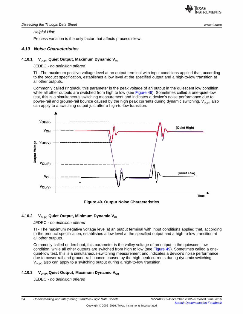
VOH(P)
VOH
VOH(V)
VOL(P)
VOL
VOL(V)
Ou
tpu
tV
olt
ag
e
(Quiet High)
(Quiet Low)
Time
Dissecting the TI Logic Data Sheet www.ti.com
54 SZZA036C–December 2002–Revised June 2016Submit Documentation Feedback
Copyright © 2002–2016, Texas Instruments Incorporated
Understanding and Interpreting Standard-Logic Data Sheets
Helpful Hint:
Process variation is the only factor that affects process skew.
4.10 Noise Characteristics
4.10.1 VOL(P) Quiet Output, Maximum Dynamic VOL
JEDEC - no definition offered
TI - The maximum positive voltage level at an output terminal with input conditions applied that, accordingto the product specification, establishes a low level at the specified output and a high-to-low transition atall other outputs.
Commonly called ringback, this parameter is the peak voltage of an output in the quiescent low condition,while all other outputs are switched from high to low (see Figure 49). Sometimes called a one-quiet-lowtest, this is a simultaneous switching measurement and indicates a device's noise performance due topower-rail and ground-rail bounce caused by the high peak currents during dynamic switching. VOL(P) alsocan apply to a switching output just after a high-to-low transition.
Figure 49. Output Noise Characteristics
4.10.2 VOL(V) Quiet Output, Minimum Dynamic VOL
JEDEC - no definition offered
TI - The maximum negative voltage level at an output terminal with input conditions applied that, accordingto the product specification, establishes a low level at the specified output and a high-to-low transition atall other outputs.
Commonly called undershoot, this parameter is the valley voltage of an output in the quiescent lowcondition, while all other outputs are switched from high to low (see Figure 49). Sometimes called a one-quiet-low test, this is a simultaneous-switching measurement and indicates a device's noise performancedue to power-rail and ground-rail bounce caused by the high peak currents during dynamic switching.VOL(V) also can apply to a switching output during a high-to-low transition.
4.10.3 VOH(P) Quiet Output, Maximum Dynamic VOH
JEDEC - no definition offered
www.ti.com Dissecting the TI Logic Data Sheet
55SZZA036C–December 2002–Revised June 2016Submit Documentation Feedback
Copyright © 2002–2016, Texas Instruments Incorporated
Understanding and Interpreting Standard-Logic Data Sheets
TI - The maximum positive voltage level at an output terminal with input conditions applied that, accordingto the product specification, establish a high level at the specified output and a low-to-high transition at allother outputs.
Commonly called overshoot, this parameter is the peak voltage of an output in the quiescent highcondition, while all other outputs are switched from low to high (see Figure 49). Sometimes called a one-quiet-high test, this is a simultaneous-switching measurement and indicates a device's noise performancedue to power-rail and ground-rail bounce caused by the high peak currents during dynamic switching.VOH(P) also can apply to a switching output during a low-to-high transition.
4.10.4 VOH(V) Quiet Output, Minimum Dynamic VOH
JEDEC - no definition offered
TI - The minimum positive voltage level at an output terminal with input conditions applied that, accordingto the product specification, establishes a high level at the specified output and a low-to-high transition atall other outputs.
Commonly called ringback, this parameter is the valley voltage of an output in the quiescent highcondition, while all other outputs are switched from low to high (see Figure 49). Sometimes called a one-quiet-high test, this is a simultaneous-switching measurement and indicates a device's noise performancedue to power-rail and ground-rail bounce caused by the high peak currents during dynamic switching.VOH(V) also can apply to a switching output just after a low-to-high transition.
4.10.5 VIH(D) High-Level Dynamic Input VoltageJEDEC - no definition offered
TI - An input voltage during dynamic switching conditions within the more positive (less negative) of thetwo ranges of values used to represent the binary variables.
NOTE: A minimum is specified that is the least positive value of high-level input voltage for whichoperation of the logic element within specification limits is to be expected.
High-level dynamic input voltage is a measurement of the shift of the input threshold due to noisegenerated while under the multiple-outputs-switching condition, with outputs operating in phase. This testis package and test-environment sensitive.
4.10.6 VIL(D) Low-Level Dynamic Input VoltageJEDEC - no definition offered
TI - An input voltage during dynamic switching conditions within the less positive (more negative) of thetwo ranges of values used to represent the binary variables.
NOTE: A maximum is specified that is the most positive value of low-level input voltage for whichoperation of the logic element within specification limits is to be expected.
Low-level dynamic input voltage is a measurement of the shift of the input threshold due to noisegenerated while under the multiple-outputs-switching condition, with outputs operating in phase. This testis package and test-environment sensitive.
4.11 Operating Characteristics
4.11.1 Cpd Power-Dissipation CapacitanceJEDEC - no definition offered
TI - This parameter is the equivalent capacitance used to determine the no-load dynamic powerdissipation per logic function for CMOS devices. PD = Cpd VCC
2 f + ICC VCC
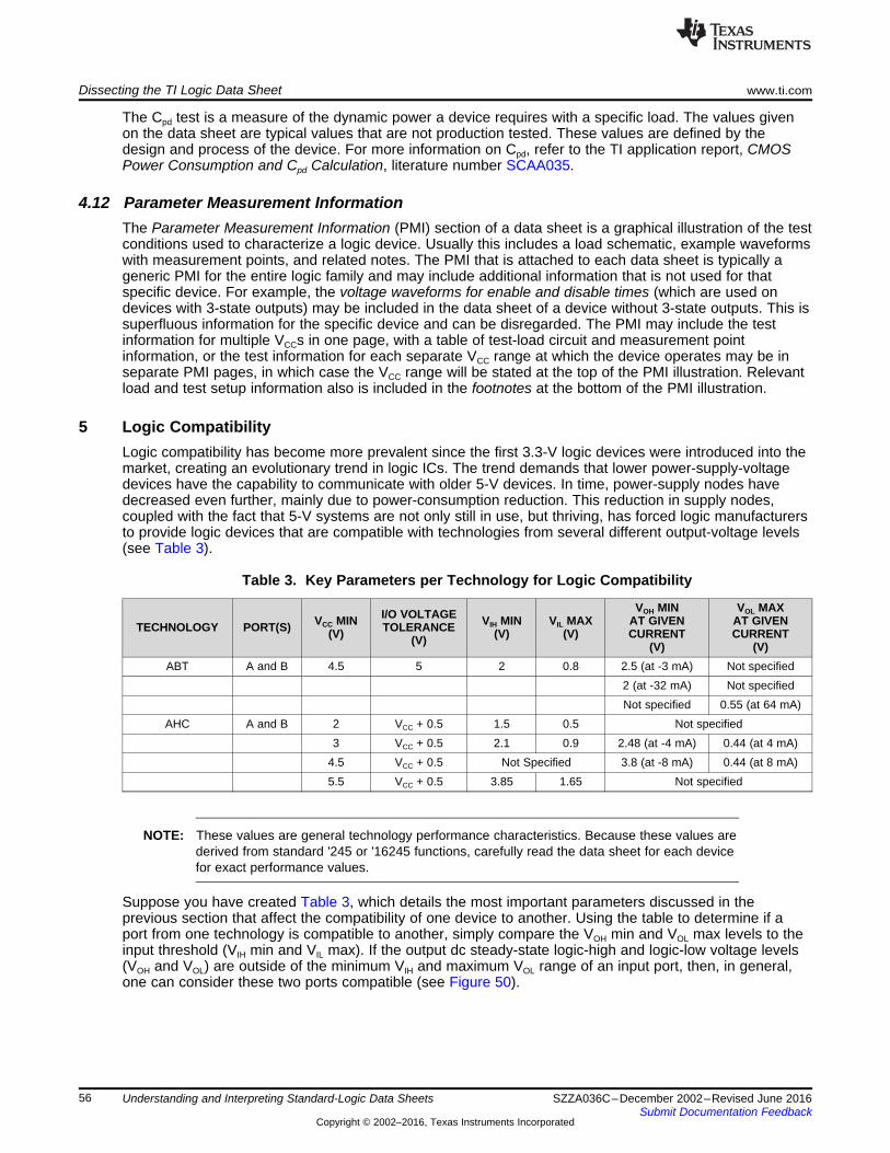
Dissecting the TI Logic Data Sheet www.ti.com
56 SZZA036C–December 2002–Revised June 2016Submit Documentation Feedback
Copyright © 2002–2016, Texas Instruments Incorporated
Understanding and Interpreting Standard-Logic Data Sheets
The Cpd test is a measure of the dynamic power a device requires with a specific load. The values givenon the data sheet are typical values that are not production tested. These values are defined by thedesign and process of the device. For more information on Cpd, refer to the TI application report, CMOSPower Consumption and Cpd Calculation, literature number SCAA035.
4.12 Parameter Measurement InformationThe Parameter Measurement Information (PMI) section of a data sheet is a graphical illustration of the testconditions used to characterize a logic device. Usually this includes a load schematic, example waveformswith measurement points, and related notes. The PMI that is attached to each data sheet is typically ageneric PMI for the entire logic family and may include additional information that is not used for thatspecific device. For example, the voltage waveforms for enable and disable times (which are used ondevices with 3-state outputs) may be included in the data sheet of a device without 3-state outputs. This issuperfluous information for the specific device and can be disregarded. The PMI may include the testinformation for multiple VCCs in one page, with a table of test-load circuit and measurement pointinformation, or the test information for each separate VCC range at which the device operates may be inseparate PMI pages, in which case the VCC range will be stated at the top of the PMI illustration. Relevantload and test setup information also is included in the footnotes at the bottom of the PMI illustration.
5 Logic CompatibilityLogic compatibility has become more prevalent since the first 3.3-V logic devices were introduced into themarket, creating an evolutionary trend in logic ICs. The trend demands that lower power-supply-voltagedevices have the capability to communicate with older 5-V devices. In time, power-supply nodes havedecreased even further, mainly due to power-consumption reduction. This reduction in supply nodes,coupled with the fact that 5-V systems are not only still in use, but thriving, has forced logic manufacturersto provide logic devices that are compatible with technologies from several different output-voltage levels(see Table 3).
Table 3. Key Parameters per Technology for Logic Compatibility
TECHNOLOGY PORT(S) VCC MIN(V)
I/O VOLTAGETOLERANCE
(V)VIH MIN
(V)VIL MAX
(V)
VOH MINAT GIVENCURRENT
(V)
VOL MAXAT GIVENCURRENT
(V)ABT A and B 4.5 5 2 0.8 2.5 (at -3 mA) Not specified
2 (at -32 mA) Not specifiedNot specified 0.55 (at 64 mA)
AHC A and B 2 VCC + 0.5 1.5 0.5 Not specified3 VCC + 0.5 2.1 0.9 2.48 (at -4 mA) 0.44 (at 4 mA)
4.5 VCC + 0.5 Not Specified 3.8 (at -8 mA) 0.44 (at 8 mA)5.5 VCC + 0.5 3.85 1.65 Not specified
NOTE: These values are general technology performance characteristics. Because these values arederived from standard '245 or '16245 functions, carefully read the data sheet for each devicefor exact performance values.
Suppose you have created Table 3, which details the most important parameters discussed in theprevious section that affect the compatibility of one device to another. Using the table to determine if aport from one technology is compatible to another, simply compare the VOH min and VOL max levels to theinput threshold (VIH min and VIL max). If the output dc steady-state logic-high and logic-low voltage levels(VOH and VOL) are outside of the minimum VIH and maximum VOL range of an input port, then, in general,one can consider these two ports compatible (see Figure 50).
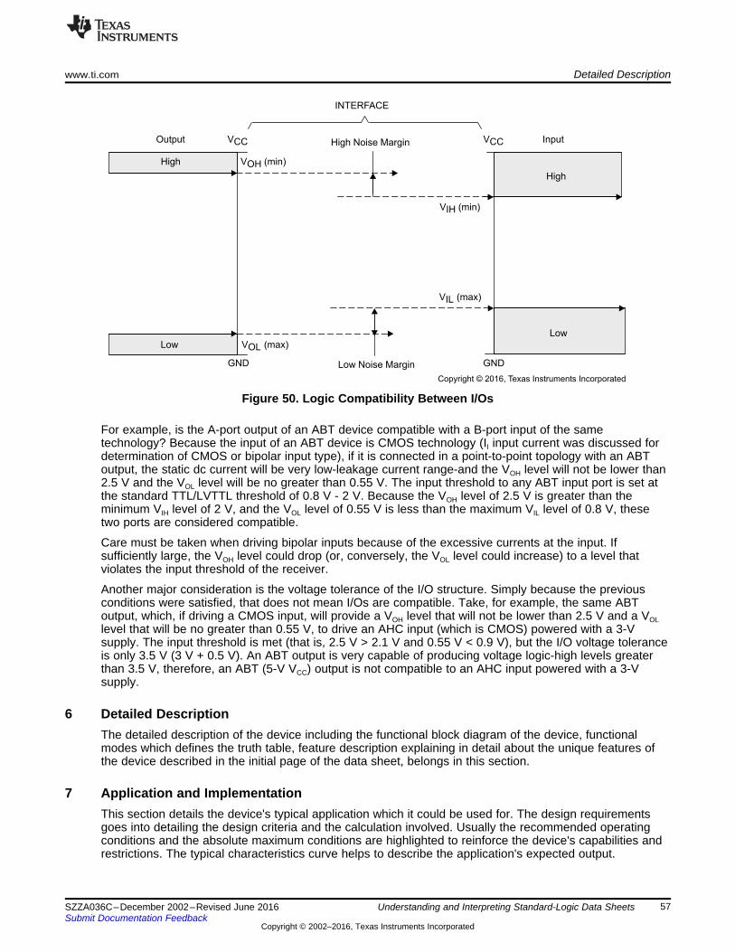
Output Input
High
High
Low
Low
High Noise Margin
Low Noise MarginGND GND
VCC VCC
VOH (min)
VOL (max)
VIL (max)
VIH (min)
INTERFACE
Copyright © 2016, Texas Instruments Incorporated
www.ti.com Detailed Description
57SZZA036C–December 2002–Revised June 2016Submit Documentation Feedback
Copyright © 2002–2016, Texas Instruments Incorporated
Understanding and Interpreting Standard-Logic Data Sheets
Figure 50. Logic Compatibility Between I/Os
For example, is the A-port output of an ABT device compatible with a B-port input of the sametechnology? Because the input of an ABT device is CMOS technology (II input current was discussed fordetermination of CMOS or bipolar input type), if it is connected in a point-to-point topology with an ABToutput, the static dc current will be very low-leakage current range-and the VOH level will not be lower than2.5 V and the VOL level will be no greater than 0.55 V. The input threshold to any ABT input port is set atthe standard TTL/LVTTL threshold of 0.8 V - 2 V. Because the VOH level of 2.5 V is greater than theminimum VIH level of 2 V, and the VOL level of 0.55 V is less than the maximum VIL level of 0.8 V, thesetwo ports are considered compatible.
Care must be taken when driving bipolar inputs because of the excessive currents at the input. Ifsufficiently large, the VOH level could drop (or, conversely, the VOL level could increase) to a level thatviolates the input threshold of the receiver.
Another major consideration is the voltage tolerance of the I/O structure. Simply because the previousconditions were satisfied, that does not mean I/Os are compatible. Take, for example, the same ABToutput, which, if driving a CMOS input, will provide a VOH level that will not be lower than 2.5 V and a VOLlevel that will be no greater than 0.55 V, to drive an AHC input (which is CMOS) powered with a 3-Vsupply. The input threshold is met (that is, 2.5 V > 2.1 V and 0.55 V < 0.9 V), but the I/O voltage toleranceis only 3.5 V (3 V + 0.5 V). An ABT output is very capable of producing voltage logic-high levels greaterthan 3.5 V, therefore, an ABT (5-V VCC) output is not compatible to an AHC input powered with a 3-Vsupply.
6 Detailed DescriptionThe detailed description of the device including the functional block diagram of the device, functionalmodes which defines the truth table, feature description explaining in detail about the unique features ofthe device described in the initial page of the data sheet, belongs in this section.
7 Application and ImplementationThis section details the device's typical application which it could be used for. The design requirementsgoes into detailing the design criteria and the calculation involved. Usually the recommended operatingconditions and the absolute maximum conditions are highlighted to reinforce the device's capabilities andrestrictions. The typical characteristics curve helps to describe the application's expected output.
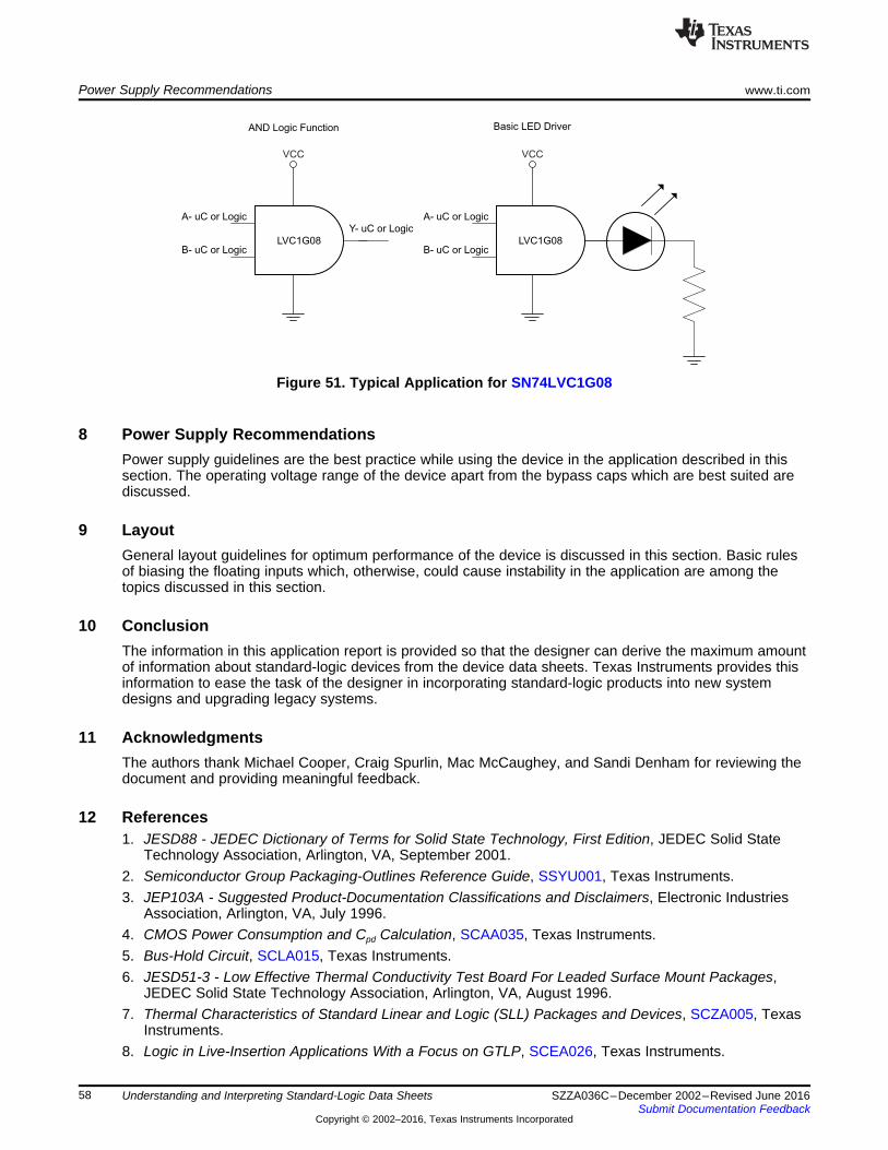
LVC1G08
A- uC or Logic
B- uC or Logic
Basic LED Driver
A- uC or Logic
B- uC or Logic
Y- uC or Logic
AND Logic Function
LVC1G08
VCC VCC
Power Supply Recommendations www.ti.com
58 SZZA036C–December 2002–Revised June 2016Submit Documentation Feedback
Copyright © 2002–2016, Texas Instruments Incorporated
Understanding and Interpreting Standard-Logic Data Sheets
Figure 51. Typical Application for SN74LVC1G08
8 Power Supply RecommendationsPower supply guidelines are the best practice while using the device in the application described in thissection. The operating voltage range of the device apart from the bypass caps which are best suited arediscussed.
9 LayoutGeneral layout guidelines for optimum performance of the device is discussed in this section. Basic rulesof biasing the floating inputs which, otherwise, could cause instability in the application are among thetopics discussed in this section.
10 ConclusionThe information in this application report is provided so that the designer can derive the maximum amountof information about standard-logic devices from the device data sheets. Texas Instruments provides thisinformation to ease the task of the designer in incorporating standard-logic products into new systemdesigns and upgrading legacy systems.
11 AcknowledgmentsThe authors thank Michael Cooper, Craig Spurlin, Mac McCaughey, and Sandi Denham for reviewing thedocument and providing meaningful feedback.
12 References1. JESD88 - JEDEC Dictionary of Terms for Solid State Technology, First Edition, JEDEC Solid State
Technology Association, Arlington, VA, September 2001.2. Semiconductor Group Packaging-Outlines Reference Guide, SSYU001, Texas Instruments.3. JEP103A - Suggested Product-Documentation Classifications and Disclaimers, Electronic Industries
Association, Arlington, VA, July 1996.4. CMOS Power Consumption and Cpd Calculation, SCAA035, Texas Instruments.5. Bus-Hold Circuit, SCLA015, Texas Instruments.6. JESD51-3 - Low Effective Thermal Conductivity Test Board For Leaded Surface Mount Packages,
JEDEC Solid State Technology Association, Arlington, VA, August 1996.7. Thermal Characteristics of Standard Linear and Logic (SLL) Packages and Devices, SCZA005, Texas
Instruments.8. Logic in Live-Insertion Applications With a Focus on GTLP, SCEA026, Texas Instruments.
www.ti.com References
59SZZA036C–December 2002–Revised June 2016Submit Documentation Feedback
Copyright © 2002–2016, Texas Instruments Incorporated
Understanding and Interpreting Standard-Logic Data Sheets
9. Dynamic Output Control (DOC™) Circuitry Technology and Applications, SCEA009, TexasInstruments.
10. Implications of Slow or Floating CMOS Inputs, SCBA004, Texas Instruments.11. JESD51-7 - High Effective Thermal Conductivity Test Board For Leaded Surface Mount Packages,
JEDEC Solid State Technology Association, Arlington, VA, February 1999.12. Power-Up 3-State (PU3S) Circuits in TI Standard Logic Devices, SZZA033
IMPORTANT NOTICE FOR TI DESIGN INFORMATION AND RESOURCES
Texas Instruments Incorporated (‘TI”) technical, application or other design advice, services or information, including, but not limited to,reference designs and materials relating to evaluation modules, (collectively, “TI Resources”) are intended to assist designers who aredeveloping applications that incorporate TI products; by downloading, accessing or using any particular TI Resource in any way, you(individually or, if you are acting on behalf of a company, your company) agree to use it solely for this purpose and subject to the terms ofthis Notice.TI’s provision of TI Resources does not expand or otherwise alter TI’s applicable published warranties or warranty disclaimers for TIproducts, and no additional obligations or liabilities arise from TI providing such TI Resources. TI reserves the right to make corrections,enhancements, improvements and other changes to its TI Resources.You understand and agree that you remain responsible for using your independent analysis, evaluation and judgment in designing yourapplications and that you have full and exclusive responsibility to assure the safety of your applications and compliance of your applications(and of all TI products used in or for your applications) with all applicable regulations, laws and other applicable requirements. Yourepresent that, with respect to your applications, you have all the necessary expertise to create and implement safeguards that (1)anticipate dangerous consequences of failures, (2) monitor failures and their consequences, and (3) lessen the likelihood of failures thatmight cause harm and take appropriate actions. You agree that prior to using or distributing any applications that include TI products, youwill thoroughly test such applications and the functionality of such TI products as used in such applications. TI has not conducted anytesting other than that specifically described in the published documentation for a particular TI Resource.You are authorized to use, copy and modify any individual TI Resource only in connection with the development of applications that includethe TI product(s) identified in such TI Resource. NO OTHER LICENSE, EXPRESS OR IMPLIED, BY ESTOPPEL OR OTHERWISE TOANY OTHER TI INTELLECTUAL PROPERTY RIGHT, AND NO LICENSE TO ANY TECHNOLOGY OR INTELLECTUAL PROPERTYRIGHT OF TI OR ANY THIRD PARTY IS GRANTED HEREIN, including but not limited to any patent right, copyright, mask work right, orother intellectual property right relating to any combination, machine, or process in which TI products or services are used. Informationregarding or referencing third-party products or services does not constitute a license to use such products or services, or a warranty orendorsement thereof. Use of TI Resources may require a license from a third party under the patents or other intellectual property of thethird party, or a license from TI under the patents or other intellectual property of TI.TI RESOURCES ARE PROVIDED “AS IS” AND WITH ALL FAULTS. TI DISCLAIMS ALL OTHER WARRANTIES ORREPRESENTATIONS, EXPRESS OR IMPLIED, REGARDING TI RESOURCES OR USE THEREOF, INCLUDING BUT NOT LIMITED TOACCURACY OR COMPLETENESS, TITLE, ANY EPIDEMIC FAILURE WARRANTY AND ANY IMPLIED WARRANTIES OFMERCHANTABILITY, FITNESS FOR A PARTICULAR PURPOSE, AND NON-INFRINGEMENT OF ANY THIRD PARTY INTELLECTUALPROPERTY RIGHTS.TI SHALL NOT BE LIABLE FOR AND SHALL NOT DEFEND OR INDEMNIFY YOU AGAINST ANY CLAIM, INCLUDING BUT NOTLIMITED TO ANY INFRINGEMENT CLAIM THAT RELATES TO OR IS BASED ON ANY COMBINATION OF PRODUCTS EVEN IFDESCRIBED IN TI RESOURCES OR OTHERWISE. IN NO EVENT SHALL TI BE LIABLE FOR ANY ACTUAL, DIRECT, SPECIAL,COLLATERAL, INDIRECT, PUNITIVE, INCIDENTAL, CONSEQUENTIAL OR EXEMPLARY DAMAGES IN CONNECTION WITH ORARISING OUT OF TI RESOURCES OR USE THEREOF, AND REGARDLESS OF WHETHER TI HAS BEEN ADVISED OF THEPOSSIBILITY OF SUCH DAMAGES.You agree to fully indemnify TI and its representatives against any damages, costs, losses, and/or liabilities arising out of your non-compliance with the terms and provisions of this Notice.This Notice applies to TI Resources. Additional terms apply to the use and purchase of certain types of materials, TI products and services.These include; without limitation, TI’s standard terms for semiconductor products http://www.ti.com/sc/docs/stdterms.htm), evaluationmodules, and samples (http://www.ti.com/sc/docs/sampterms.htm).
Mailing Address: Texas Instruments, Post Office Box 655303, Dallas, Texas 75265Copyright © 2017, Texas Instruments Incorporated