Embed Size (px)
Citation preview
Unconventional Micro-Manufacturing
and Integration Technologies
Frank Niklaus

Outline
• Background
• Micro-Manufacturing and Integration Research
• Heterogeneous 3D Integration for MEMS & NEMS
• Integration and Packaging for MEMS
• Nanofabrication Technologies and Graphene NEMS
• Summary

Sweden’s largest technical
university:
• More than 13,000 full-time
students.
• Close to 1,800 research
students.
• Around 3,500 full-time
positions.
KTH Royal Institute of Technology

Micro and Nanosystem Integration
Prof. Frank Niklaus
Lab-on-a-Chip and Polymer Devices
Prof. Wouter van der Wijngaart
Microwave and THz MEMS
Prof. Joachim Oberhammer
Biomedical Devices
Assoc. Prof. Niclas Roxhed
Bioelectric Hybrid Systems
Ass. Prof. Anna Herland
Photonic MEMS
Ass. Prof. Kristinn Gylfason
Head: Prof. Göran Stemme
Department of Micro- and Nanosystems

Göran Stemme Prof.
Wouter van der Wijngaart Prof.
Joachim Oberhammer Prof.
Niclas Roxhed Assoc. Prof.
Kristinn B. Gylfason Assis. Prof.
Anna Herland Assis.Prof.
Hans Sohlström Assoc. Prof.
Tommy Haraldsson Researcher
Ilya Anoshkin Researcher
Oleksandr Glubokov Researcher
Jonas Hansson Researcher
Petr Makhalov Researcher
Umer Shah Researcher
Simon Bleiker Researcher
James Campion
Valentin Dubois
Alessandro Enrico
Xuge Fan
Jessica Liljeholm
Linnea Gustafsson
Maoxiang Guo
Weijin Guo
PhD Students
Erika Appel Admin. Ass.
Ulrika Pettersson Admin. Ass.
Mikael Bergqvist Technician
Cecilia Aronsson Technician
Researchers
Support
Thanks to all Colleagues at KTH !
Gabriel Lenk
Floria Ottonello Briano
Simone Pagliano
Arne Quellmalz
Mina Rajabi
Federico Ribet
Stephan Schröder
Serguei Smirnov
Fritzi Töpfer
Alexander Vastesson
Xiaojing Wang
Reza Zandi Shafagh
Zhou Xiamo
Zhao Xinghai
Carlos Errando Herranz
Emre Iseri
Staffan Johansson
Aleksandr Krivovitca
Laila Ladhani
Miku Laakso
Torben Last

Micro and Nanosystem Integration Group
• 8 Ph.D. students at MST
• 2 industrial Ph.D. students at
SenseAir and Silex Microsystems
• 1 postdoc and 3 contributing
senior researchers

• Heterogeneous 3D Integration
Technologies for MEMS and NEMS
• Integration and Packaging for MEMS
• Nanofabrication Technologies and
Graphene-Based NEMS
• Femotosecond Laser-Based
Micromachining for MEMS & NEMS
Four Research Topics
CMOS IC
MEMS
Schematic of Pressure Sensor
Cavity Covered
with Graphene
Membrane
Wire Bond
Pads
Silicon
SiO2

• Heterogeneous 3D Integration for
MEMS & NEMS
• Integration and Packaging for MEMS
• Nanomanufacturing Technologies
and Graphene NEMS
CMOS IC
MEMS
Research Topics in Group

Heterogeneous 3D Integration for MEMS & NEMS
• New MEMS designs, functionalities and material combinations.
• High performance MEMS materials on standard foundry ICs.
• Very high integration densities for smaller and cheaper components.
Motivation
CMOS IC
MEMS

3D Integrated MEMS on ICs
Commercial Examples: Invensense (gyro), mCube (accel.)

Via-Last Heterogeneous 3D Integration Platform
Advantages
• No wafer-to-wafer alignment.
• Extreme reduction of via and dimensions (sub µm) possible.
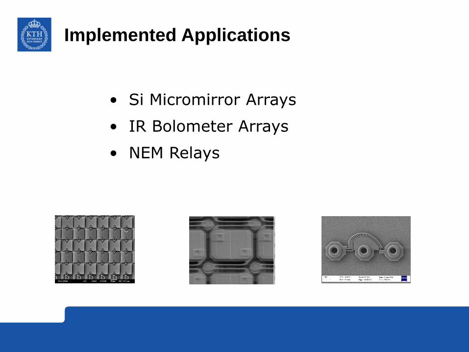
Implemented Applications
• Si Micromirror Arrays
• IR Bolometer Arrays
• NEM Relays

• Step and repeat maskless lithography.
• 1 million mirrors (mirror size 16 x 16 µm2).
• Single mirror actuation with
underlying CMOS.
• Analogue tilt actuation in 16 steps
(gray-tones) possible.
Tilting Micro-Mirror Arrays (SLMs) for Maskless
DUV Lithography Systems
Source: Zimmer, Fraunhofer IPMS

Via-Last Heterogeneous Integration
for Mono-Crystalline Si Mirrors on CMOS
SOI Wafer
CMOS IC
Si Device Layer

Glue
Si Mirror Integration: Dispense Glue
CMOS IC
SOI Wafer

Glue
Si Mirror Integration: Adhesive Wafer Bonding
CMOS IC
SOI Wafer

Glue
Si Mirror Integration: Sacrificial Wafer Thinning
CMOS IC

Glue
Si Mirror Integration: Removal of SiO2 Etch-Stop
CMOS IC

Glue
Si Mirror Integration: Via Etch
CMOS IC

Glue
Si Mirror Integration: Via Formation
CMOS IC

Glue
Si Mirror Integration: Mirror Formation
CMOS IC

Si Mirror Integration: Mirror Release
CMOS IC

1 M-pixel Mono-Si Mirror Array on CMOS
Distance
Holders
Addressing
Electrode
Mirror
Membrane
Torsional Hinges
Posts
(Vias)
Zimmer, Lapisa to appear MEMS 2011

Wave-front correction using piston-type mirror arrays
SLMs for Adaptive Optics in Astronomy and Microscopy
Source: Lapisa, KTH and Zimmer, Fraunhofer IPMS
CMOS IC
MEMS

2-Layer SLMs Fabrication Process
Lapisa, M., Zimmer, F., Stemme, G., Gehner, A., & Niklaus, F. (2013). Heterogeneous 3D integration of hidden hinge micromirror
arrays consisting of two layers of monocrystalline silicon. Journal of Micromechanics and Microengineering, 23(7), 075003.
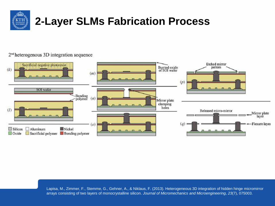
2-Layer SLMs Fabrication Process
Lapisa, M., Zimmer, F., Stemme, G., Gehner, A., & Niklaus, F. (2013). Heterogeneous 3D integration of hidden hinge micromirror
arrays consisting of two layers of monocrystalline silicon. Journal of Micromechanics and Microengineering, 23(7), 075003.

Via-Last Heterogeneous Integration for Piston-
Mirrors Using Two-Step Layer Transfer
Lapisa, M., Zimmer, F., Stemme, G., Gehner, A., & Niklaus, F. (2013). Heterogeneous 3D integration of hidden hinge micromirror
arrays consisting of two layers of monocrystalline silicon. Journal of Micromechanics and Microengineering, 23(7), 075003.

Bolometer Array for IR Imaging
Forsberg, Fredrik, et al. "CMOS-integrated Si/SiGe quantum-well infrared microbolometer focal plane arrays manufactured with
very large-scale heterogeneous 3-D integration." IEEE Journal of Selected Topics in Quantum Electronics 21.4 (2015): 30-40.

Design of QW Si/SiGe IR Bolometer
Forsberg, Fredrik, et al. "CMOS-integrated Si/SiGe quantum-well infrared microbolometer focal plane arrays manufactured with
very large-scale heterogeneous 3-D integration." IEEE Journal of Selected Topics in Quantum Electronics 21.4 (2015): 30-40.

Heterogeneously Integrated 17 µm pitch QW SiGe Bolometers on Fan-Out-Wafers
Forsberg, Fredrik, et al. "CMOS-integrated Si/SiGe quantum-well infrared microbolometer focal plane arrays manufactured with
very large-scale heterogeneous 3-D integration." IEEE Journal of Selected Topics in Quantum Electronics 21.4 (2015): 30-40.

Functional Double-Layer 25 µm pitch IR Bolometers on 0.35 µm CMOS
Forsberg, Fredrik, et al. "CMOS-integrated Si/SiGe quantum-well infrared microbolometer focal plane arrays manufactured with
very large-scale heterogeneous 3-D integration." IEEE Journal of Selected Topics in Quantum Electronics 21.4 (2015): 30-40.

Integration of NEM Switches
Goal:
NEM switch on top of 2 metal layer
interconnect wafer
Method:
Metal anchors for
mechanical stability and
electrical connection

Heterogeneous Integration Process

Heterogeneous Integration Process

Challenges
Etching of Anchor holes
- Use hard mask to etch through
different materials a
How do you know
when to stop etching?

Integrated Moni-Si NEM Switches
Qin, T., Bleiker, S. J., Rana, S., Niklaus, F., & Pamunuwa, D. (2018). Performance Analysis of
Nanoelectromechanical Relay-Based Field-Programmable Gate Arrays. IEEE Access.

• Heterogeneous 3D Integration for
MEMS & NEMS
• Integration and Packaging for MEMS
• Nanomanufacturing Technologies
and Graphene NEMS
Research Topics in Group

Wafer-Level Vacuum Sealing Using Cold Metal Welding in
Combination with Solder Bumps
Antelius, M., Stemme, G., & Niklaus, F. (2011). Small footprint wafer-level vacuum packaging using
compressible gold sealing rings. Journal of Micromechanics and Microengineering, 21(8), 085011.
• Au sealing ring prevents solder vaport enter cavity.
• Solder bumps provide bond strength.

Wafer-Level Vacuum Sealing: Process Flow
Antelius, M., Stemme, G., & Niklaus, F. (2011). Small footprint wafer-level vacuum packaging using
compressible gold sealing rings. Journal of Micromechanics and Microengineering, 21(8), 085011.

Wafer-Level Low-Temperature Vacuum Sealing Using 8 µm Wide Copper Rings

Wafer-Level Low-Temperature Vacuum Sealing Using Copper Sealing

Wire Bonded TSVs
• Low-cost for low to medium TSV density
• Enable high aspect ratio TSV formation
• No lithography (mask-less) TSV formation
• Low temperature budget approach

TSVs Manufacturing Using Wire Bonding

Gold TSVs with Aspect Ratios > 20
Schröder, Stephan, et al. "Very high aspect ratio through silicon vias (TSVs) using wire bonding." Solid-State Sensors,
Actuators and Microsystems (TRANSDUCERS & EUROSENSORS XXVII), 2013 Transducers & Eurosensors XXVII:
The 17th International Conference on. IEEE, 2013.

Sealing of Liquids in MEMS Cavities Using Cold Metal Plugging
Image source: Antelius, Proc Transducers 2011, KTH

Image source: Antelius, Proc Transducers 2011, KTH
Sealing of Liquids in MEMS Cavities Using Cold Metal Plugging

Wafer-Level Vacuum Sealing Using Cold Metal Plugging
Image source: Antelius, Proc Transducers 2011, KTH

Wafer-Level Vacuum Sealing Using Cold Metal Plugging
Image source: Antelius, Proc Transducers 2011, KTH

Wire Bonded Infrared Emitter
• Joule-heated suspended Kanthal filament
• Integration using an automated wire bonding tool
• Mechanical fixation and placement by
– Attachment structures for free air ball & wire
– Guiding posts
Schröder, Stephan, et al. "Fabrication of an infrared emitter using a generic integration platform
based on wire bonding." Journal of Micromechanics and Microengineering 26.11 (2016): 115010.

Filament Integration Results
1.Filament Emitter
2.Free air ball attachment
5.Electrical contact
4.Filament attachment
3.Filament placement

Fabrication of High-Aspect Ratio TSVs by Magnetic Assembly of Metal Studs
Image source: Fischer, Proc MEMS 2011, KTH

High-Aspect Ratio Nickel TSVs
Image source: Fischer, Proc MEMS 2011, KTH
Robotic Magnetic Self-assembly of TSVs
Image source: Fischer, Proc MEMS 2011, KTH
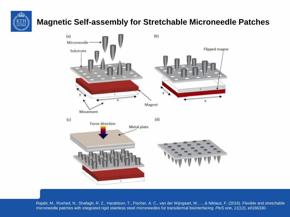
Magnetic Self-assembly for Stretchable Microneedle Patches
Rajabi, M., Roxhed, N., Shafagh, R. Z., Haraldson, T., Fischer, A. C., van der Wijngaart, W., ... & Niklaus, F. (2016). Flexible and stretchable
microneedle patches with integrated rigid stainless steel microneedles for transdermal biointerfacing. PloS one, 11(12), e0166330.

Magnetic Self-assembly for Stretchable Microneedle Patches
Combination of :
Stretchable and flexible substrate for comfort; and
Sharp and stiff needles for reliable penetration
Rajabi, M., Roxhed, N., Shafagh, R. Z., Haraldson, T., Fischer, A. C., van der Wijngaart, W., ... & Niklaus, F. (2016). Flexible and stretchable
microneedle patches with integrated rigid stainless steel microneedles for transdermal biointerfacing. PloS one, 11(12), e0166330.

• Heterogeneous 3D Integration for
MEMS & NEMS
• Integration and Packaging for MEMS
• Nanomanufacturing Technologies
and Graphene NEMS
Research Topics in Group
Schematic of Pressure Sensor
Cavity Covered
with Graphene
Membrane
Wire Bond
Pads
Silicon
SiO2

Nanogap Electrodes
Major problem: Extremely difficult to realize
Nanogap electronics:
Require sub-3 nm wide gaps between electrodes !

Scalable Fabrication of Crack-Defined Nanogap
Electrodes
Valentin Dubois, Frank Niklaus, and Göran Stemme. "Crack‐Defined Electronic Nanogaps." Adv. Mater. (2016).
• Control of gap size: 1-100 nm
• Realization of tunneling junctions
• Massively parallel fabrication

L1 L2
L3
Valentin Dubois, Frank Niklaus, and Göran Stemme. "Crack‐Defined Electronic Nanogaps." Adv. Mater. (2016).
Control of Gap Size
1 μm in electrode bridge length 3.1 nm in nanogap width

Valentin Dubois, Frank Niklaus, and Göran Stemme. "Crack‐Defined Electronic Nanogaps." Adv. Mater. (2016).
Nanogap Tunneling Junctions
Demonstration of quantum tunneling
in crack-defined nanogap electrodes
down to sub-1 nm in titanium nitride
(TiN) and gold (Au)
Electron quantum tunneling occurs with sub-3 nm nanogaps

Massively Parallel Fabrication
Density up to 7,000,000 junctions per cm2
Compatible with wafer-scale processes
and CMOS integration

Schematic of Pressure Sensor
Cavity Covered
with Graphene
Membrane
Wire Bond
Pads
Silicon
SiO2
Graphene-Based NEMS: Pressure Sensing
Smith, A. D., Niklaus, F., Paussa, A., Vaziri, S., Fischer, A. C., Sterner, M., ... & Ostling, M. (2013).
Electromechanical piezoresistive sensing in suspended graphene membranes. Nano letters, 13(7), 3237-3242.

Graphene-Integration in NEMS
Smith, A. D., Niklaus, F., Paussa, A., Vaziri, S., Fischer, A. C., Sterner, M., ... & Ostling, M. (2013).
Electromechanical piezoresistive sensing in suspended graphene membranes. Nano letters, 13(7), 3237-3242.

Graphene-NEMS Pressure Sensing
Smith, A. D., Niklaus, F., Paussa, A., Vaziri, S., Fischer, A. C., Sterner, M., ... & Ostling, M. (2013).
Electromechanical piezoresistive sensing in suspended graphene membranes. Nano letters, 13(7), 3237-3242.
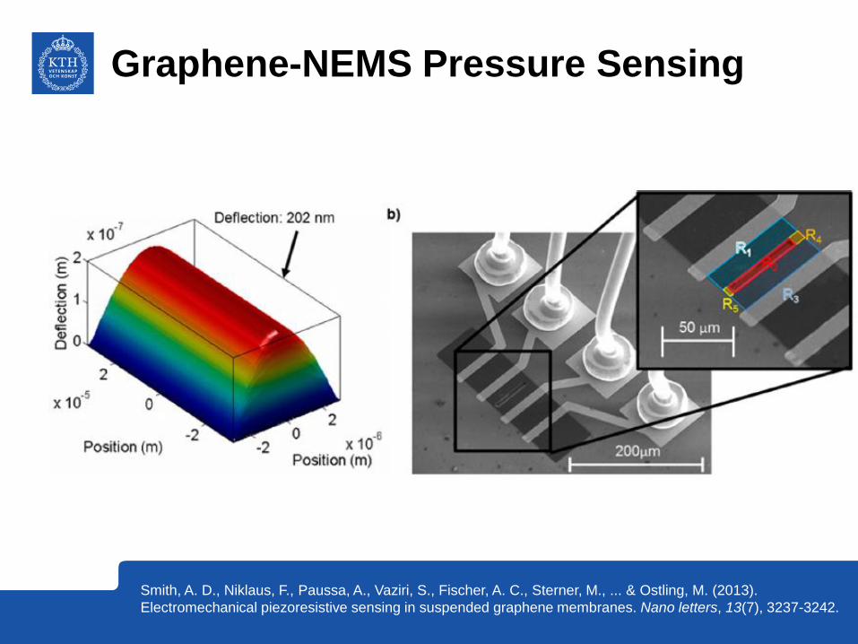
Graphene-NEMS Pressure Sensing
Smith, A. D., Niklaus, F., Paussa, A., Vaziri, S., Fischer, A. C., Sterner, M., ... & Ostling, M. (2013).
Electromechanical piezoresistive sensing in suspended graphene membranes. Nano letters, 13(7), 3237-3242.

Summary
• Heterogeneous 3D integration platform for micro-mirrors,
IR bolometers and NEMS relays.
• Wafer-level vacuum packaging, and wire bonding and magnetic
assembly for wire integration in MEMS.
• Graphene NEMS pressure sensors and nanofabrication
technologies for tunnelling junctions.

Collaboration Partners
Acknowledgements
Funding Sources


3D Printing Process for Si Nano Devices
A.C. Fischer et al., Advanced Functional Materials, 2012.

3D Printing of Si Micro and Nano Devices
A.C. Fischer et al., Advanced Functional Materials, 2012

3D Printing of Si Micro and Nano Devices
A.C. Fischer et al., Advanced Functional Materials, 2012

Cross Section of Si Nano Devices
A.C. Fischer et al., Advanced Functional Materials, 2012

3-Layer 3D Printed Si Micro-Structures

Resolution Limits of 3D Si Printed Nano-Structures
• Line-width resolution of
33 nm demonstrated.
• Line-width resolution of
20 nm with FIB writing,
reported in literature.
• Layer thickness on the
order of 35-70 nm.
A.C. Fischer et al., Advanced Functional Materials, 2012