Embed Size (px)
Citation preview

Nanoscale
PAPER
Cite this: Nanoscale, 2017, 9, 1475
Received 24th October 2016,Accepted 9th December 2016
DOI: 10.1039/c6nr08347a
www.rsc.org/nanoscale
Ultrafast carrier dynamics in bimetallicnanostructure-enhanced methylammoniumlead bromide perovskites†
Holly F. Zarick,a,b Abdelaziz Boulesbaa,c Alexander A. Puretzky,c Eric M. Talbert,a,b
Zachary R. DeBra,a,b Naiya Soetan,a,b David B. Geoheganc and Rizia Bardhan*a,b
In this work, we examine the impact of hybrid bimetallic Au/Ag core/shell nanostructures on the carrier
dynamics of methylammonium lead tribromide (MAPbBr3) mesoporous perovskite solar cells (PSCs).
Plasmon-enhanced PSCs incorporated with Au/Ag nanostructures demonstrated improved light harvest-
ing and increased power conversion efficiency by 26% relative to reference devices. Two complementary
spectral techniques, transient absorption spectroscopy (TAS) and time-resolved photoluminescence
(trPL), were employed to gain a mechanistic understanding of plasmonic enhancement processes. TAS
revealed a decrease in the photobleach formation time, which suggests that the nanostructures improve
hot carrier thermalization to an equilibrium distribution, relieving hot phonon bottleneck in MAPbBr3perovskites. TAS also showed a decrease in carrier decay lifetimes, indicating that nanostructures enhance
photoinduced carrier generation and promote efficient electron injection into TiO2 prior to bulk recombi-
nation. Furthermore, nanostructure-incorporated perovskite films demonstrated quenching in steady-
state PL and decreases in trPL carrier lifetimes, providing further evidence of improved carrier injection in
plasmon-enhanced mesoporous PSCs.
Introduction
An unprecedented rise in efficiency has been observed inmethylammonium lead trihalide (MAPbX3, X = I, Cl, Br) per-ovskite solar cells (PSCs) from 3.8% in 2009 to >20% in early2016.1–5 The inexpensive materials and low cost of solution-based processing6 make this class of perovskites amenable toscalable manufacturing and has the potential to be a seriouscontender for utility-scale solar power. MAPbI3-based PSCshave been a primary focus due to their near-complete visiblelight absorption in films <1 μm and their fast charge extractionrates.7,8 However, the poor stability of MAPbI3 and rapid degra-dation in humidity has remained a major obstacle for commer-cialization,9,10 necessitating complex encapsulation tech-niques.11 MAPbBr3 is a promising alternative to MAPbI3 with alarge 2.2 eV bandgap, which gives rise to a high open circuitvoltage (Voc ∼1.2–1.5 V)12,13 and makes it an ideal material for
tandem devices. Their long exciton diffusion length (>1.2 μm)enables good charge transport in devices.14 In addition,MAPbBr3 demonstrates higher stability towards air andmoisture due to its stable cubic phase and low ionic mobilityrelative to the pseudocubic MAPbI3, in which inherent latticestrain provides an avenue for increased diffusion.11,14–16
However, a relatively large exciton binding energy, EB, (76 meV)and poor light absorption beyond its band edge at 550 nm haslimited the efficiencies for MAPbBr3 solar cells.
11,15,17,18
Metal nanostructures provide an effective route to improvelight harvesting in solar cells, enhance optical absorption, andincrease carrier generation, resulting in higher efficiency.19
The localized surface plasmon resonances (LSPRs) supportedby metal nanostructures simultaneously give rise to intenseelectromagnetic near-fields and light scattering in the farfields,82 which have been harnessed to enhance the perform-ance of both planar20–22 and mesoporous solar cells.23–27
Recent work on plasmon-enhanced PSCs has suggested that inaddition to improved scattering and near field coupling, metalnanostructures also reduce the exciton binding energy (EB)and enable better charge separation.28–31 Highly polarizablemetal nanostructures have also been shown to favor radiativedecay processes, increasing the optical path length of incidentphotons by the reabsorption of emitted radiation within theperovskite absorber layer.32 Additionally, by controlling theposition and polarization of metal nanostructures, the result-
†Electronic supplementary information (ESI) available. See DOI: 10.1039/c6nr08347a
aDepartment of Chemical and Biomolecular Engineering, Vanderbilt University,
Nashville, TN 37235, USA. E-mail: [email protected] of Mechanical Engineering, Vanderbilt University, Nashville, TN 37235,
USAcCenter for Nanophase Materials Sciences, Oak Ridge National Laboratory,
Oak Ridge, TN 37831, USA
This journal is © The Royal Society of Chemistry 2017 Nanoscale, 2017, 9, 1475–1483 | 1475
Publ
ishe
d on
14
Dec
embe
r 20
16. D
ownl
oade
d by
Van
derb
ilt U
nive
rsity
Lib
rary
on
15/0
6/20
17 1
8:04
:14.
View Article OnlineView Journal | View Issue

ing LSPR modes can couple with the perovskite and give riseto strong light–matter interactions at the metal/perovskiteinterface.33 In our previous work, we demonstrated the use ofbimetallic gold/silver core/shell nanostructures (Au/Ag NSs) forenhancing the performance of organic photovoltaics22 as wellas dye-sensitized solar cells.23 Here we investigate the inter-actions of Au/Ag NSs with MAPbBr3 perovskites in the meso-porous device architecture. The engineered shape and con-trolled composition of the Au/Ag NSs gives rise to panchro-matic light absorption, and their sharp edges and cornersresult in intense electric fields attributable to the quasistaticlightning-rod effect.34–37 These spectral characteristics of Au/Ag NSs result in broadband light absorption above the bandedge of MAPbBr3, a phenomenon useful for device performance.We integrated Au/Ag NSs within the mesoporous TiO2 layer ofMAPbBr3 PSCs, examined the device performance, and corre-lated these trends with the carrier dynamics of MAPbBr3 withboth transient absorption spectroscopy (TAS) and time-resolvedphotoluminescence (trPL). Our results demonstrate that carrierlifetimes significantly decrease for both TAS and trPL in thepresence of the bimetallic nanostructures. The enhancementsobserved in the presence of Au/Ag NSs in both photocurrent andincident photon to charge conversion efficiency (IPCE) ofMAPbBr3 PSCs correlate well with the decrease in carrier life-times. We attributed these effects in carrier dynamics toenhanced photoinduced charge generation and rapid electroninjection into TiO2 in the presence of the plasmonic nano-structures, as well as reduced recombination and improvementin hot carrier thermalization in the perovskite.
Experimental methods
All reagents were purchased from Sigma Aldrich unless other-wise specified and were used as received without further puri-fication. All the H2O used for substrate preparation and nano-structure synthesis was ultrapure H2O (18.2 MΩ) obtainedfrom a Milli-Q Direct-Q 3UV system. All work done under aninert atmosphere was conducted in a nitrogen filled MBraunLabStar glovebox (<0.5 ppm O2).
Au/Ag nanostructure synthesis
Au/Ag nanostructures were synthesized following a proceduredescribed in our previous work.38 Au nanocube cores were pre-pared following a seed-mediated growth method in which Auseeds were formed by adding 600 μL of ice cold, freshly pre-pared 10 mM NaBH4 to a solution containing 7.5 mL of100 mM CTAB, 2.75 mL H2O, and 0.8 mL of 10 mM HAuCl4.The solution was stirred vigorously for 1 minute before beingtransferred to a 35 °C water bath where it was left to stay forone hour. The seeds were then diluted by a factor of 10 withwater before being added to a growth solution composed of6.4 mL of 100 mM CTAB, 0.8 mL of 10 mM HAuCl4, and3.8 mL of 100 mM ascorbic acid that were added sequentiallyto 32 mL of ultrapure H2O. Post-Au seed addition, the mixturewas mixed by gentle inversion, and then left to react un-
disturbed for 5 hours in a 35 °C water bath. A ligand exchangewas performed on the Au NC cores before Ag layer growth wasperformed: Au NCs were centrifuged at 1100 RCF for 15 minutesin 7.5 mL aliquots, the supernatant was removed, and the par-ticles were washed and soaked in 3.75 mL of 20 mM CTAC for15 minutes. This was repeated for a total of 3 spins and two15 minute soaks. The final CTAC-capped Au NC pellet was redis-persed in 500 μL of water to make the final precursor solutionfor Au growth. Typically, 400 μL of the Au NC precursor wasadded to 10 mL of 20 mM CTAC along with 100 μL of 10 mMKBr. This was mixed by inversion and heated in a 65 °C waterbath for 10 minutes before adding into 100 μL of 10 mM AgNO3
and 300 μL of 100 mM ascorbic acid, mixing again by inversion,and placing it back in the 65 °C water bath for two hours.
Silica-coating of Au/Ag nanostructures
Au/Ag NSs were capped with a thin ∼4 nm layer of silica bymodifying a previously described procedure.39 In a 50 mLround bottom flask, 30 mL of as-prepared Au/Ag NSs were firstfunctionalized with 400 μL of a freshly prepared 1 mM3-aminopropyltrimethoxysilane (APTMS) solution for15 minutes at room temperature while stirring at ∼500 RPM.A 0.54 wt% solution of sodium silicate was adjusted to pH∼10.2 with 5 N HCl followed by injecting 500 μL into theAPTMS-functionalized Au nanocubes. The reaction mixturewas stirred for 3 minutes at room temperature and then trans-ferred to a 50 °C oil bath and stirred for 4.5 hours to form theuniform silica shell. The reaction was quenched by placing thecoated nanostructures in the fridge overnight. The particleswere then centrifuged at 900 RCF (×2) and washed once withwater prior to imaging and device incorporation.
Perovskite Layer Fabrication
MAPbBr3-sensitized layers were deposited on either glass forTAS and PL testing or FTO-glass for full device characteriz-ation, including JV and IPCE testing. Glass and FTO-glass sub-strates were cleaned by sonication for 30 min in a 2 vol% solu-tion of Hellmanex in H2O, rinsed first with H2O and then IPA,and then sonicated for an additional 15 minutes in a 1 : 1 v/vmixture of IPA/acetone. The substrates were then rinsed withIPA, dried with N2, and plasma treated for 15 minutes immedi-ately before use. A ∼50 nm layer of compact TiO2 was de-posited on the substrates by hydrolyzing 40 mM TiCl4 at 70 °C.The substrates were removed from the TiCl4 bath after onehour, rinsed with H2O and EtOH, dried with N2, and thenannealed at 500 °C for 15 minutes. Mesoporous TiO2 was de-posited by spin coating a diluted solution of 18NRT Dyesolpaste (1 : 2 : 1 by weight of EtOH : α-terpineol : Dyesol) at 2500RPM for 60 seconds, dried on a 100 °C hot plate, and then sin-tered at 500 °C for 30 minutes. Plasmon-enhanced sampleswere prepared in the same manner; however, washed and con-centrated pellets of silica-coated Au/Ag NSs were added directlyto the diluted Dyesol paste to the desired concentrations andmixed until homogeneous before spin coating. All mesoporouslayers received a 40 mM TiCl4 post-treatment at 70 °C for30 minutes, were rinsed with H2O and EtOH, dried with N2,
Paper Nanoscale
1476 | Nanoscale, 2017, 9, 1475–1483 This journal is © The Royal Society of Chemistry 2017
Publ
ishe
d on
14
Dec
embe
r 20
16. D
ownl
oade
d by
Van
derb
ilt U
nive
rsity
Lib
rary
on
15/0
6/20
17 1
8:04
:14.
View Article Online

and fired in air at 500 °C for 15 minutes. At this point, allmesoporous TiO2 substrates were transferred into an inertenvironment. MAPbBr3 films were then prepared following amodified two-step sequential deposition process.40 First, a 1 Msolution of PbBr2 in DMF was stirred on a 75 °C hot plate for20 minutes and filtered with a 0.45 μm PTFE filter immediatelybefore use. TiO2 substrates were heated to 75 °C prior to spin-coating 200 μL of the filtered PbBr2 solution at 2500 RPM for60 seconds followed by a 30 minute annealing at 75 °C. Oncecooled post-annealing, the substrates were dipped in IPA for1–2 s before being placed in a heated (50 °C) solution consist-ing of 15 mg mL−1 MABr (Dyesol) in IPA for 10 minutes,rinsed with IPA, and annealed again at 75 °C for 30 minutes.
PSC fabrication
Full devices were fabricated on FTO-sensitized substrates fol-lowing a typical fabrication process.41 An HTM was preparedby the addition of 72.3 mg of SpiroMeOTAD (2,29,7,79-tetrakis(N,N-di-p-methoxyphenylamine)-9,9-spirobifluorene, EMD), 29 μLof 4-tert-butylpyridine, 18 μl of a 520 mg mL−1 LiTFSI (lithiumbis(trifluoromethylsulphonyl)imide) in acetonitrile solution, and29 μL of a 300 mg mL−1 tris(2-(1H-pyrazol-1-yl)-4-tert-butylpyri-dine)cobalt(III) bis(trifluoromethylsulphonyl)imide (Lumtec) inacetonitrile solution to 1 mL chlorobenzene.41 100 μL of theHTM solution was then deposited on top of MAPbBr3-sensitizedTiO2 films at 3000 RPM for 30 s. The samples were left overnightin darkness and dry air before 80 nm Au contacts were depositedvia thermal evaporation in 8 mm diameter circles utilizingshadow masks in an Angstrom Amod system.
Materials characterization
All optical absorbance spectra were taken using a Varian Cary5000 UV-vis NIR spectrophotometer. Scanning and trans-mission electron microscopy were conducted with a ZeissMerlin and an FEI Tecnai Osiris, respectively. Characterizationof power conversion performance of full device PSCs was con-ducted with a Newport solar simulator and a Metrohm potentio-stat. Each cell received 1 sun (100 mW cm−2) of power from thesolar simulator at AM 1.5 over equivalent areas of 0.081 cm2
and was tested at a scan rate of 50 mV s−1. An average of 10devices were tested for each sample type. Incident photon con-version efficiency (IPCE) measurements were conducted with a6 W Fianium fiber laser supercontinuum source coupled with aFianium acousto-optic tunable filter to filter out the desiredexcitation wavelength from the white light source.
Transient absorption measurements
Femtosecond transient absorption measurements wereconducted using a home-built pump–probe setup based on afemtosecond laser system that utilizes seed pulses from atitanium sapphire oscillator (Micra, Coherent), amplified by aTi:Sapphire amplifier (Legend USP-HE, Coherent) to provide800 nm femtosecond pulses (2.5 mJ per pulse) operating at a1 kHz repetition rate with ∼45 fs pulse durations. The Legendamplifier is pumped by using a Nd:YLF laser (Evolution-30,Coherent). A small portion of the output of the amplifier
(∼4 μJ per pulse) is focused on a sapphire window (2 mmthick) to generate a white light continuum (WLC) probe(450–900 nm). To minimize temporal chirp in the spectrallybroad WLC probe, a set of parabolic mirrors was used to colli-mate and focus the WLC on the sample. The transmittedprobe was focused onto 100 μm core fiber coupled with aspectrometer/CCD (USB2000ES, Ocean Optics). The pumppulse at 400 nm is generated by doubling ∼50 μJ per pulse ofthe 800 nm fundamental in a BBO crystal. The pump beampasses through a delay-line to allow control of time-delaybetween the pump and the probe. In order to measure theabsorbance changes between every two successive laser shots,the pump beam was chopped at a frequency of 500 Hz. At thesample, the spot sizes of the pump and probe pulses were100 μm and 50 μm, respectively. The pump energy fluence atthe sample was ∼ 5 μJ cm−2.
Photoluminescence measurements
The photoluminescence (PL) spectra were recorded using aspectrometer (Acton SP2300) equipped with a CCD (PrincetonInstruments, Pixis 256), which was coupled to a microscope.The time-resolved PL spectra were recorded by using a timecorrelated single photon counting (TCSPC) module (HoribaScientific with Picosecond Photon Detection Module, PPD-850and Fluorohub model: Horiba JY IBH). The PPD-850 wasmounted to a second port of the same spectrometer. MAPbBr3-sensitized TiO2 films, with and without Au/Ag NSs, wereexcited at 400 nm using a second harmonic signal of a Ti:sapphire laser (Coherent, Mira 900, 5 ps pulse length, 76 MHzrepetition rate). To match TCSPC requirements, the laserrepetition rate was reduced to ∼5 kHz using a pulse picker(Coherent). The output from the pulse picker was frequencydoubled using an ultrafast harmonic generator (Coherent5-050) and directed into a microscope to illuminate the filmsthrough a 100× microscope objective (beam spot size ∼1 µm).All films were initially exposed to 400 nm light for ∼20 min inorder to stabilize the samples.
Results and discussion
The MAPbBr3 PSCs were fabricated by infiltrating the perovs-kite within a ∼500 nm mesoporous titania (mp-TiO2) layer fol-lowing a modified two-step sequential deposition process (seeExperimental methods for details).40 The mp-TiO2 provides anideal scaffold for perovskite crystal growth and for embeddingthe bimetallic nanostructures, and provides a pathway forselective charge collection.42,43 The incorporated Au/Ag NSswere synthesized following a seed-mediated growth methoddescribed in our previous work.38 The NSs were coated with aconformal ∼5 nm layer of silica (silica-coated Au/Ag NSs,Fig. 1c), then homogeneously mixed throughout the meso-porous TiO2 layer (Fig. 1a) allowing close proximity of the NSsto the MAPbBr3 crystals to enable plasmonic enhancement.The silica minimizes charge recombination at the perovskite/nanoparticle interface by prohibiting direct conduction of
Nanoscale Paper
This journal is © The Royal Society of Chemistry 2017 Nanoscale, 2017, 9, 1475–1483 | 1477
Publ
ishe
d on
14
Dec
embe
r 20
16. D
ownl
oade
d by
Van
derb
ilt U
nive
rsity
Lib
rary
on
15/0
6/20
17 1
8:04
:14.
View Article Online

plasmon electrons into the perovskite. It also prevents Ostwaldripening during the high temperature TiO2 annealing pro-cesses, and avoids degradation of the NSs by the halide ions inthe perovskite.23,24,32 The color-enhanced cross-sectional SEMimage shown in Fig. 1b (non-color modified in the ESI,Fig. S2†) depicts the relative morphology and layer thicknessesof the MAPbBr3 PSCs. The representative TEM images of Au/AgNSs shown in Fig. 1c (silica-coated) and Fig. S1† (without silicacoating) illustrate the two distinct geometries that form duringsynthesis, nanocubes and nanopyramids, with distinct plasmon
resonances centered at 540 nm and 615 nm correlating with thetwo geometries, respectively (Fig. 1d). The two absorbancepeaks of the mixed NSs promote light scattering above thebandgap of MAPbBr3 as well as provide complementary broad-band absorption spanning the entire visible spectrum.
The light harvesting ability of the Au/Ag NSs within theMAPbBr3 PSCs was probed by comparing the absorbances ofreference, MAPbBr3-sensitized TiO2 films without nano-structures, to TiO2/MAPbBr3 mesoporous films containing twodifferent densities of silica-coated Au/Ag NSs, 0.5 wt% and1.0 wt% (Fig. 2a). An increase in absorbance was observed withthe increasing nanostructure density in the 410–540 nm spec-tral range where the plasmon resonances of the bimetallicnanostructures overlap with the absorption of the MAPbBr3perovskite. This indicates enhanced radiative light trapping inthe photoactive layer as a result of the Au/Ag NSs. Whilechanges in absorbance above 550 nm are subtle, detailed ana-lysis of relative absorbance enhancement (Fig. S3a†) demon-strates that Au/Ag NSs promote broadband light absorptioncomplementary to where MAPbBr3 absorbs light. The absorp-tion enhancement we observed experimentally in our work iscomparable to the theoretical enhancements predicted for per-ovskite active layers embedded with plasmonic metal nano-particles.44 However enhancement in solar cells is driven byseveral different factors that collectively determine the externalquantum efficiency and ultimately influences the total powerconversion efficiency. These include the photon absorptionefficiency (ηabs) which is the ratio of absorbed light to incidentlight, the exciton dissociation efficiency (ηdiss) which is theratio of photoexcited excitons that are converted to free car-riers, the charge carrier transport efficiency (ηct) which is theratio of the generated free carriers that reach the electrodeprior to recombination, and charge collection efficiency (ηcoll),the ratio of carriers that are collected after the final interfacebetween the active layer and the electrodes.22 The contributionfrom each of these factors was examined by evaluating thedevice efficiencies. We investigated the device performance ofthe PSCs by comparing the power conversion efficiencies
Fig. 1 (a) Schematic representation of a MAPbBr3 perovskite solar cellintegrated with bimetallic Au/Ag nanostructures. The nanostructures arenot shown to scale in the mesoporous TiO2 layer. A cross-sectional SEMimage of a representative reference device with an Au counter electrode(CE) is shown in (b). Coloring of the layers has been added for clarity.(c) TEM image of the bimetallic nanostructures coated with a conformal∼5 nm layer of silica. The normalized absorption spectrum of MAPbBr3-sensitized TiO2 films compared to the normalized extinction spectrumof the Au/Ag NSs is shown in (d); spectra are normalized to the peaks at530 and 535 nm, respectively.
Fig. 2 (a) Optical absorption spectra of mesoporous TiO2 infiltrated with MAPbBr3 and integrated with varying concentrations of silica-coatedAu/Ag nanostructures. (b) The best and average power conversion efficiencies of devices as a function of varying concentrations of Au/Ag nano-structures (wt%). Error was calculated from standard deviations of ∼10 devices tested at each concentration. (c) IPCE of the same devices as a func-tion of excitation wavelength.
Paper Nanoscale
1478 | Nanoscale, 2017, 9, 1475–1483 This journal is © The Royal Society of Chemistry 2017
Publ
ishe
d on
14
Dec
embe
r 20
16. D
ownl
oade
d by
Van
derb
ilt U
nive
rsity
Lib
rary
on
15/0
6/20
17 1
8:04
:14.
View Article Online
(PCE’s) of full reference MAPbBr3 PSCs with the plasmon-enhanced devices containing both 0.5 and 1.0 wt% silica-coated Au/Ag NSs (Fig. 2b). Average values and standard devi-ation for PCE were calculated from ∼10 devices for each refer-ence, 0.5 wt% Au/Ag, and 1.0 wt% Au/Ag-incorporated devices.A steady increase in PCE is observed for both 0.5 and 1.0 wt%silica-coated Au/Ag NS incorporations, with the best PCEsmeasured at 4.5% and 4.9% respectively, compared to thereference devices of 3.9% efficiency. The device parameters,Fig. S4,† show that the measured 26% increase in efficiencywith Au/Ag nanostructures is not only attributed to an increasein the short circuit current density, Jsc, correlated with ηabs andηdiss, but also the fill factor (FF) and open circuit voltage (Voc)correlated with ηct and ηcoll. This suggests that the nano-structures improve light harvesting in the devices, as well asincrease charge transfer and reduce carrier recombination.However further improvements in ηabs, ηdiss, ηct, and ηcollcollectively could potentially result in higher overall efficien-cies in both reference and plasmonic devices.
While several studies have focused on plasmonic enhance-ment of PSCs,28,29,31,32,45–48 the carrier dynamics in metalnanostructure-incorporated PSCs remain poorly understood.Here we have employed a combination of TAS and trPL tounderstand the carrier dynamics in MAPbBr3 reference films(non-enhanced) and investigate the impact on the excitongeneration and charge recombination in MAPbBr3 in the pres-ence of Au/Ag NSs. TAS studies were performed on films ofMAPbBr3-infiltrated in the mp-TiO2 layer with a compact-TiO2
electron acceptor layer (without SpiroMeOTAD). The sampleswere pumped at 400 nm to fill the perovskite conduction
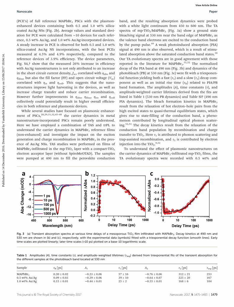
band, and the resulting absorption dynamics were probedwith a white light continuum from 450 to 600 nm. The TAspectra of mp-TiO2/MAPbBr3 (Fig. 3a) show a ground statebleaching signal at 530 nm near the band edge of MAPbBr3 asthe valence band electrons are excited to the conduction bandby the pump pulse.49 A weak photoinduced absorption (PIA)signal at 490 nm is also observed, which is a result of stimu-lated absorption above the saturated conduction band states.50
Our TA evolutionary spectra are in good agreement with thosereported in the literature for MAPbBr3.
51,52 The normalizeddecay of the PIA band at 490 nm (Fig. 3b) and dynamics of thephotobleach (PB) at 530 nm (Fig. 3c) were fit with a triexponen-tial function yielding both a fast (τ1) and a slow (τ2) decay com-ponent as well as an initial rise time (τR) related to PIA/PBband formation. The amplitudes (A), time constants (τ), andamplitude-weighted carrier lifetimes derived from the fits arelisted in Table 1 (530 nm PB dynamics) and Table SI† (490 nmPIA dynamics). The bleach formation kinetics in MAPbBr3result from the relaxation of hot electron–hole pairs from thehigh excited states to quasi-thermal equilibrium states, whichgives rise to state-filling of the conduction band, a pheno-menon contributed by longitudinal optical phonon scatter-ing.52,53 The decay kinetics result from the relaxation of theconduction band population by recombination and chargetransfer to TiO2. Here τ1 is attributed to phonon scattering andtrap-assisted recombination, and τ2 is contributed by electroninjection into the TiO2.
8,52
To understand the effect of plasmonic nanostructures onthe carrier dynamics of MAPbBr3-infiltrated mp-TiO2 films, theTA evolutionary spectra were recorded with 0.5 wt% and
Fig. 3 (a) Transient absorption spectra at various time delays of a mesoporous TiO2 film infiltrated with MAPbBr3. Decay kinetics at 490 nm and530 nm are shown in (b) and (c), respectively, with the experimental data (symbols) fitted with a triexponential decay function (smooth lines). Earlytime scales are plotted linearly; later time scales (>10 ps) plotted on a base-10 logarithmic scale.
Table 1 Amplitudes (A), time constants (τ), and amplitude-weighted lifetimes (τavg) derived from triexponential fits of the transient absorption forthe different samples at the photobleach band located at 530 nm
Sample τR [ps] A1 τ1 [ps] A2 τ2 [ps] τavg [ps]
MAPbBr3 0.20 ± 0.02 −0.23 ± 0.06 57 ± 16 −0.76 ± 0.06 312 ± 21 2530.5 wt% Au/Ag 0.09 ± 0.03 −0.29 ± 0.06 39 ± 10 −0.64 ± 0.07 225 ± 20 1671.0 wt% Au/Ag 0.15 ± 0.01 −0.44 ± 0.01 25 ± 2 −0.55 ± 0.01 168 ± 6 104
Nanoscale Paper
This journal is © The Royal Society of Chemistry 2017 Nanoscale, 2017, 9, 1475–1483 | 1479
Publ
ishe
d on
14
Dec
embe
r 20
16. D
ownl
oade
d by
Van
derb
ilt U
nive
rsity
Lib
rary
on
15/0
6/20
17 1
8:04
:14.
View Article Online

1.0 wt% Au/Ag NSs (Fig. 4a and b). Whereas the peak positionsof the PB state of the Au/Ag NS-incorporated samples arecomparable to that of the reference (Fig. 3), the bandwidth ofthe PB increases with the increasing particle density of NSs.The broadening of the PB state may be attributed to a morerapid band filling in the nanostructure-incorporated films rela-tive to the reference films. Sharma et al.51 observed a similarphenomenon in MAPbBr3 thin films with increasing pumpenergy fluence as higher carrier densities result in a saturationof conduction band levels near the bandgap. This is also sup-ported in our data from the decreasing maximum bleachamplitude with the increasing particle density (Fig. 3a and 4a,b), as more rapid thermalization would lead to less optimiz-ation of energy states. It is also possible, however, that thebroadening may be attributed to the formation of trap states.In the TA spectra of perovskites, trap states are characterizedby a weak bleach absorption with a broad distribution thatdecays red-shifted, or below the energy, of the optical bandgap of the perovskite.54 These traps states have longer decaytimes than the PB state and are populated by the relaxation ofhot carriers and can result in the blocking of weakly allowedtransitions during excitation.55 While the weak sub-bandgapbleach of the 1.0 wt% sample identifies some trap-state filling,the peak broadening more strongly indicates an increased rateof electron–phonon coupling. The enhanced PCE of devices(Fig. 2) at these concentrations supports this hypothesis as thecollection of free carriers is enhanced. Trapped excitons havehigher exciton binding energies (EB),
55 decreasing the prob-
ability of exciton dissociation and increasing the probability ofrecombination, manifesting as decreased efficiency in thesolar cells. Since plasmonic nanoparticles have been reportedto lower the EB (or induce resonant energy transfer to enableexciton dissociation),29–31 the observed increases in photo-current for plasmon-enhanced PSCs likely stem from a combi-nation of electromagnetic effects and reduced EB.
The recoveries of the PB at 530 nm were normalized and fitwith a triexponential decay function for all samples (Fig. 4d);the amplitudes and lifetimes derived from the fits are shownin Table 1. The carrier dynamics at 490 nm are provided in theESI (Fig. S5 and Table S1†). We first compared the bleach for-mation time, τR, between the reference and the plasmon-enhanced samples, which has been attributed to the thermal-ization of hot carriers after photoexcitation.56,57 During ther-malization in MAPbBr3, optical hot phonons are generated bythe coupling of phonons with hot electrons that subsequentlyslows the cooling of carriers and increases the τR.
52 In MAPbI3systems, this phenomenon has been termed the ‘hot phononbottleneck effect’.58,59 As seen in Table 1, both plasmon-enhanced samples, containing 0.5 and 1.0 wt% silica-coatedAu/Ag NSs, exhibit faster thermalization times compared tothe reference MAPbBr3. This faster τR lifetime likely resultsfrom plasmon–phonon coupling between the nanostructuresand the perovskite which limits the coupling of phonons withhot electrons and relieves the hot phonon bottleneck. Plasmon–phonon coupling has been studied extensively in various metal–semiconductor systems.60–64 In our nanostructure/MAPbBr3system, relief of this hot phonon bottleneck should also aid inphonon propagation within the active layer, reflected as adecrease in the longer (τ2) calculated lifetimes (Table 1). It isnoteworthy that relative to the reference MAPbBr3 (0.2 ps), theτR of 0.5 wt% Au/Ag NSs (0.09 ps) is more reduced than that ofthe τR of 1.0 wt% Au/Ag NSs (0.15 ps). This indicates thatplasmon–phonon coupling is very sensitive to the nanostructuredensity; at a 1.0 wt% concentration, the sample may have ahigher degree of particle aggregation where interparticle coup-ling likely supersedes plasmon–phonon coupling and results inless relief of the phonon bottleneck.
The amplitude-weighted lifetimes, τavg, of the PB recoverykinetics at 530 nm significantly decrease with the increasingparticle density, from 253 ps for the reference MAPbBr3 to167 ps and 104 ps for the 0.5 wt% and 1.0 wt% Au/Ag NSs.A systematic decrease in τ1 and τ2 is observed as well. Thissuggests that the bimetallic nanostructures amplify light trap-ping in the MAPbBr3 active layer of PSCs, by both near fieldcoupling of the nanostructures with MAPbBr3 as well as farfield coupling of scattered light into the active layer.65–69 Theperovskite crystals are exposed to an increased photon fluxgenerated by the intense near fields localized at the sharpedges and corners of vicinal Au/Ag NSs, giving rise to highercarrier densities. The elevated carrier densities are expected toweaken trap-assisted recombination, specifically when thedensity of charge carriers far exceeds that of the trap states,resulting in shorter carrier lifetimes.70 Further the ideal size ofthese bimetallic nanostructures and the presence of the Ag
Fig. 4 Transient absorption spectra at various time delays of meso-porous TiO2/MAPbBr3 and those containing 0.5 wt% (a) and 1.0 wt%(b) of silica-coated Au/Ag NSs. Normalized TA spectra at the maximumbleach peak (∼1 ps time delay) comparing the reference and the Au/AgNS-enhanced samples are shown in (c). (d) Decay kinetics at 530 nm forthe reference and Au/Ag NS-incorporated samples. Decay kinetics areshown with the experimental data (symbols) fitted with a triexponentialdecay function (smooth lines). Early time scales are plotted linearly; latertime scales (>10 ps) plotted on a base-10 logarithmic scale.
Paper Nanoscale
1480 | Nanoscale, 2017, 9, 1475–1483 This journal is © The Royal Society of Chemistry 2017
Publ
ishe
d on
14
Dec
embe
r 20
16. D
ownl
oade
d by
Van
derb
ilt U
nive
rsity
Lib
rary
on
15/0
6/20
17 1
8:04
:14.
View Article Online

layer amplify their ability to scatter light, facilitating enhancedlight harvesting and the light is reemitted by the MAPbBr3active layer, which improves the optical path length. Theenhanced light trapping, in conjunction with improvedphonon propagation from relief of the hot phonon bottleneckvia plasmon–phonon coupling, enhance the number of freecarries generated, which results in more electrons being avail-able to efficiently transfer to the TiO2 conduction band. Thisimplies that the presence of metal nanostructures leads tofaster electron injection into TiO2, suppressing the recombina-tion in the bulk and resulting in a shorter carrier lifetime asreflected in the TAS results.
To further understand the role of Au/Ag NSs on the carrierdynamics of the MAPbBr3 films, we supplemented our pro-posed mechanisms by measuring the steady-state PL and trPLof the reference and plasmon-enhanced films. The MAPbBr3reference films exhibited a narrow photoluminescence peakcentered around the bandgap (Fig. 5a) of MAPbBr3 analogousto that demonstrated in the literature.71,72 In the presence ofthe nanostructures, a significant reduction in the PL intensityis observed; where the PL is quenched by ∼32% and ∼65%with 0.5 wt% and 1.0 wt% silica-coated Au/Ag NSs, respect-ively. This quenching in steady-state PL indicates that non-radiative decay pathways are favored with the increasing nano-structure density, which decreases exciton decay by recombina-tion and suppression of PL.32,73 Our result suggests that thepresence of the nanostructures promotes more efficient chargecarrier extraction at MAPbBr3 and mp-TiO2 interfaces, attri-butable to the intense electric fields generated by the nano-structures.28,74 Furthermore, the enhanced non-radiative decaypathways in the presence of the nanostructures also facilitatebelow band gap energy transfer into the nearby semi-
conductor, specifically plasmon resonant energy transfer(PRET). PRET, which has been extensively studied in a range ofsolar energy conversion systems,19 occurs when the energylocalized in plasmon oscillations around the nanostructure istransferred to surrounding semiconductor and inducescharge separation and carrier generation.19,75,76 PRET does notinvolve direct electron injection into the semiconductor and isnot limited by band alignment or the presence of thin insulat-ing interlayers; therefore the quenching in steady-state PL mayreflect resonant energy transfer from the dipole–dipole relax-ation of excited plasmons in the nanostructures into both themp-TiO2 and MAPbBr3 crystals. In addition to PRET, hot elec-tron transfer (HET) is another non-radiative enhancementmechanism that occurs when plasmons decay via energeticrelaxation and create hot electron/hole pairs.77,78 These hot elec-trons can gain enough energy to overcome the Schottky barrierat metal/semiconductor interfaces and inject directly into thesemiconductor conduction band.19 However, we do not antici-pate any HET in our system due to the presence of ∼5 nm silicainsulating layer coating the nanostructures (Fig. 1c); since theelectron tunneling barrier of silica is <3 nm,79–81 this will prohi-bit HET from the nanostructures to the perovskite.
The trends in steady-state PL follow the PL decay observedwith room temperature trPL measurements of the referenceMAPbBr3 and nanostructure-incorporated films (Fig. 5b).Carrier lifetimes, shown in Table 2, were obtained by fittingthe experimental data with a biexponential decay function.The average PL lifetime, τavg, of the reference films decreasedfrom 2.84 ns to 1.3 ns for the 0.5 wt% Au/Ag NSs and 0.36 nsfor the 1.0 wt% Au/Ag. The reduced PL lifetimes correspondwell with the quenching in steady-state PL of MAPbBr3 in thepresence of bimetallic nanostructures, which supports ourearlier hypothesis of rapid charge transfer and reduced recom-bination at the plasmon/perovskite interface, enhancingcarrier extraction from the MAPbBr3 to TiO2. Furthermore,plasmonic nanostructures also decrease the exciton bindingenergy (EB) of perovskites; in our system the reduced EB ofMAPbBr3 by bimetallic nanostructures would also manifest assuppressed PL if charge transfer is promoted into the mp-TiO2
prior to exciton recombination in the bulk. While the exactmechanism that decreases the EB of perovskites in the pres-ence of plasmonic nanostructures is not fully understood, itopens up an exciting avenue for MAPbBr3-based devices,whose enhanced environmental stability relative to MAPbI3 isoffset in part by its higher EB. Overall, quenching of thesteady-state PL and decreases in trPL carrier lifetimes translatewell to the increased efficiencies observed for the nano-structure-incorporated PSCs (Fig. 2 and S4†).45
Fig. 5 (a) Steady-state photoluminescence spectra of mesoporous TiO2
films infiltrated with MAPbBr3 and different concentrations of silica-coated Au/Ag NSs. (b) The corresponding photoluminescence decayplots of the same samples with 400 nm excitation. Experimental data in(b) are denoted by symbols and have been fitted with a biexponentialdecay function (black lines).
Table 2 Amplitudes (A), time constants (τ), and amplitude-weighted lifetimes (τavg) derived from biexponential fits of trPL transients of each sample
Sample A1 τ1 [ns] A2 τ2 [ns] τavg [ns]
MAPbBr3 0.57 ± 0.01 1.18 ± 0.02 0.40 ± 0.01 5.25 ± 0.05 2.840.5 wt% Au/Ag 0.49 ± 0.00 0.31 ± 0.01 0.64 ± 0.00 2.05 ± 0.01 1.301.0 wt% Au/Ag 0.77 ± 0.04 0.21 ± 0.01 0.27 ± 0.03 0.79 ± 0.02 0.36
Nanoscale Paper
This journal is © The Royal Society of Chemistry 2017 Nanoscale, 2017, 9, 1475–1483 | 1481
Publ
ishe
d on
14
Dec
embe
r 20
16. D
ownl
oade
d by
Van
derb
ilt U
nive
rsity
Lib
rary
on
15/0
6/20
17 1
8:04
:14.
View Article Online

Conclusions
In summary, we boosted the efficiency of MAPbBr3-based PSCsby incorporating silica-coated Au/Ag bimetallic nanostructuresinto the mesoporous TiO2 active layer. The increased light har-vesting in the devices as determined by absorbance and IPCEmeasurements in conjunction with improvements in Jsc, Voc,and FF for plasmon-enhanced samples demonstrate strongcoupling between Au/Ag NSs and the MAPbBr3-inflitrated TiO2
active layer. Our results indicate enhanced carrier generationwith decreased recombination in the perovskite in the presenceof the nanostructures. The decreased carrier lifetimes obtainedfrom both TAS and trPL measurements and the quenchingobserved in ssPL further support our hypothesis. Lifetimesobtained from photobleach formation and recovery in transientabsorption spectra suggest that the presence of the nano-structures coupled with the MAPbBr3 improves the hot carrierthermalization to an equilibrium distribution via plasmon–phonon coupling. Decreases in lifetimes correlating with elec-tron injection suggest that the presence of Au/Ag NS enhancesphotoinduced carrier generation as a result of both strong nearfield and far field coupling of light, promoting efficient electroninjection into TiO2 prior to bulk recombination. Quenching ofsteady state PL and decreases in carrier lifetimes obtained fromtrPL, attributed in part to PRET effects and reduction in EB,provide further evidence to the improved carrier injection inplasmon-enhanced mesoporous perovskites. We envision thatthese bimetallic nanostructures can be straightforwardly trans-lated to other perovskite systems to enhance the efficiencies notonly of solar devices, but also of photodetectors and lasers.
Acknowledgements
HFZ acknowledges support from Vanderbilt UniversityDiscovery grant, NSF EPSCOR (NSF EPS1004083), NSF BRIGE(EEC 1342185), and the Department of Education for GraduateAssistance in Areas of National Need (GAANN) Fellowship undergrant number P0200A090323. EMT acknowledges the VINSE fel-lowship and Vanderbilt start-up funds. TEM images wereobtained with an instrument supported by NSF EPS 1004083.Ultrafast and photoluminescence measurements were conductedat the Center for Nanophase Materials Sciences, which is a DOEOffice of Science User Facility.
References
1 M. A. Green, K. Emery, Y. Hishikawa, W. Warta andE. D. Dunlop, Prog. Photovoltaics, 2016, 24, 3–11.
2 A. Kojima, K. Teshima, Y. Shirai and T. Miyasaka, J. Am.Chem. Soc., 2009, 131, 6050–6051.
3 M. M. Lee, J. Teuscher, T. Miyasaka, T. N. Murakami andH. J. Snaith, Science, 2012, 338, 643–647.
4 H. S. Kim, C. R. Lee, J. H. Im, K. B. Lee, T. Moehl,A. Marchioro, et al., Sci. Rep., 2012, 2, 00591.
5 C. Zuo, H. J. Bolink, H. Han, J. Huang, D. Cahen andL. Ding, Adv. Sci., 2016, 3, 1500324.
6 Y. Tong, E. Bladt, M. F. Ayguler, A. Manzi, K. Z. Milowska,V. A. Hintermayr, et al., Angew. Chem., Int. Ed., 2016, 55,13887–13892.
7 S. D. Stranks, G. E. Eperon, G. Grancini, C. Menelaou,M. J. Alcocer, T. Leijtens, L. M. Herz, A. Petrozza andH. J. Snaith, Science, 2013, 342, 341–344.
8 G. Xing, N. Mathews, S. Sun, S. S. Lim, Y. M. Lam,M. Gratzel, S. Mhaisalkar and T. C. Sum, Science, 2013, 342,344–347.
9 Y. Han, S. Meyer, Y. Dkhissi, K. Weber, J. M. Pringle,U. Bach, L. Spiccia and Y.-B. Cheng, J. Mater. Chem. A,2015, 3, 8139–8147.
10 J. Yang, B. D. Siempelkamp, D. Liu and T. L. Kelly, ACSNano, 2015, 9, 1955–1963.
11 J. H. Noh, S. H. Im, J. H. Heo, T. N. Mandal and S. I. Seok,Nano Lett., 2013, 13, 1764–1769.
12 X. Zheng, B. Chen, C. Wu and S. Priya, Nano Energy, 2015,17, 269–278.
13 C. Zuo and L. Ding, Adv. Energy Mater., 2016, 1601193.14 N. Kedem, T. M. Brenner, M. Kulbak, N. Schaefer,
S. Levcenko, I. Levine, D. Abou-Ras, G. Hodes andD. Cahen, J. Phys. Chem. Lett., 2015, 6, 2469–2476.
15 R. Sheng, A. Ho-Baillie, S. Huang, S. Chen, X. Wen, X. Haoand M. A. Green, J. Phys. Chem. C, 2015, 119, 3545–3549.
16 E. M. Talbert, H. F. Zarick, N. J. Orfield, W. Li, W. R. Erwin,Z. R. DeBra, et al., RSC Adv., 2016, 6, 86947–86954.
17 E. Edri, S. Kirmayer, D. Cahen and G. Hodes, J. Phys. Chem.Lett., 2013, 4, 897–902.
18 J. H. Heo, D. H. Song and S. H. Im, Adv. Mater., 2014, 26,8179–8183.
19 W. R. Erwin, H. F. Zarick, E. M. Talbert and R. Bardhan,Energy Environ. Sci., 2016, 9, 1577–1601.
20 F.-C. Chen, J.-L. Wu, C.-L. Lee, Y. Hong, C.-H. Kuo andM. H. Huang, Appl. Phys. Lett., 2009, 95, 013305.
21 A. P. Kulkarni, K. M. Noone, K. Munechika, S. R. Guyer andD. S. Ginger, Nano Lett., 2010, 10, 1501–1505.
22 W. R. Erwin, C. Hungerford, H. F. Zarick, E. M. Talbert,P. Arora and R. Bardhan, ACS Omega, 2016, 1, 722–729.
23 H. F. Zarick, W. R. Erwin, A. Boulesbaa, O. K. Hurd,J. A. Webb, A. A. Puretzky, D. B. Geohegan and R. Bardhan,ACS Photonics, 2016, 3, 385–394.
24 H. F. Zarick, O. Hurd, J. A. Webb, C. Hungerford, W. R. Erwinand R. Bardhan, ACS Photonics, 2014, 1, 806–811.
25 J. Qi, X. Dang, P. T. Hammond and A. M. Belcher, ACSNano, 2011, 5, 7108–7116.
26 M. D. Brown, T. Suteewong, R. S. Kumar, V. D’Innocenzo,A. Petrozza, M. M. Lee, U. Wiesner and H. J. Snaith, NanoLett., 2011, 11, 438–445.
27 S. Chang, Q. Li, X. Xiao, K. Y. Wong and T. Chen, EnergyEnviron. Sci., 2012, 5, 9444–9448.
28 Z. Lu, X. Pan, Y. L. Ma, Y. L. Zheng, D. Zhang, Q. Xu, et al.,RSC Adv., 2015, 5, 11175–11179.
29 W. Zhang, M. Saliba, S. D. Stranks, Y. Sun, X. Shi,U. Wiesner and H. J. Snaith, Nano Lett., 2013, 13, 4505–4510.
Paper Nanoscale
1482 | Nanoscale, 2017, 9, 1475–1483 This journal is © The Royal Society of Chemistry 2017
Publ
ishe
d on
14
Dec
embe
r 20
16. D
ownl
oade
d by
Van
derb
ilt U
nive
rsity
Lib
rary
on
15/0
6/20
17 1
8:04
:14.
View Article Online

30 H. Yu, J. Roh, J. Yun and J. Jang, J. Mater. Chem. A, 2016, 4,7322–7329.
31 S. Carretero-Palacios, M. E. Calvo and H. Miguez, J. Phys.Chem. C, 2015, 119, 18635–18640.
32 M. Saliba, W. Zhang, V. M. Burlakov, S. D. Stranks, Y. Sun,J. M. Ball, et al., Adv. Funct. Mater., 2015, 25, 5038–5046.
33 W. Niu, L. A. Ibbotson, D. Leipold, E. Runge, G. V. Prakashand J. J. Baumberg, Phys. Rev. B, 2015, 91, 161303.
34 C. Burda, X. Chen, R. Narayanan and M. A. El-Sayed, Chem.Rev., 2005, 105, 1025–1102.
35 K. L. Kelly, E. Coronado, L. L. Zhao and G. C. Schatz,J. Phys. Chem. B, 2003, 107, 668–677.
36 J. A. Schuller, E. S. Barnard, W. Cai, Y. C. Jun, J. S. Whiteand M. L. Brongersma, Nat. Mater., 2010, 9, 193–204.
37 S. Link and M. A. El-Sayed, Int. Rev. Phys. Chem., 2000, 19,409–453.
38 H. F. Zarick, W. R. Erwin, J. Aufrecht, A. Coppola,B. R. Rogers, C. L. Pint and R. Bardhan, J. Mater. Chem. A,2014, 2, 7088–7098.
39 W. R. Erwin, A. Coppola, H. F. Zarick, P. Arora, K. J. Millerand R. Bardhan, Nanoscale, 2014, 6, 19–22.
40 M. Kulbak, D. Cahen and G. Hodes, J. Phys. Chem. Lett.,2015, 6, 2452–2456.
41 J. Burschka, N. Pellet, S. J. Moon, R. Humphry-Baker,P. Gao, M. K. Nazeeruddin and M. Gratzel, Nature, 2013,499, 316–319.
42 C.-C. Chung, C. S. Lee, E. Jokar, J. H. Kim andE. W.-G. Diau, J. Phys. Chem. C, 2016, 120, 9619–9627.
43 T. Salim, S. Sun, Y. Abe, A. Krishna, A. C. Grimsdale andY. M. Lam, J. Mater. Chem. C, 2015, 3, 8943–8969.
44 S. Carretero-Palacios, A. Jiménez-Solano and H. Míguez,ACS Energy Lett., 2016, 1, 323–331.
45 J. Cui, C. Chen, J. Han, K. Cao, W. Zhang, Y. Shen andM. Wang, Adv. Sci., 2016, 3, 1500312.
46 B. Cai, Y. Peng, Y. B. Cheng and M. Gu, Opt. Express, 2015,23, A1700–A1706.
47 S. S. Mali, C. S. Shim, H. Kim, P. S. Patil and C. K. Hong,Nanoscale, 2016, 8, 2664–2677.
48 R. Wu, B. Yang, C. Zhang, Y. Huang, Y. Cui, P. Liu, et al.,J. Phys. Chem. C, 2016, 120, 6996–7004.
49 Y. Zhai, C. X. Sheng, C. Zhang and Z. V. Vardeny, Adv.Funct. Mater., 2016, 26, 1617–1627.
50 T. C. Sum, N. Mathews, G. Xing, S. S. Lim, W. K. Chong,D. Giovanni and H. A. Dewi, Acc. Chem. Res., 2016, 49, 294–302.
51 V. Sharma, S. Aharon, I. Gdor, C. Yang, L. Etgar andS. Ruhman, J. Mater. Chem. A, 2016, 4, 3546–3553.
52 X. Deng, X. Wen, S. Huang, R. Sheng, T. Harada, T. W. Kee,M. Green and A. Ho-Baillie, J. Phys. Chem. C, 2016, 120,2542–2547.
53 L. Wang, C. McCleese, A. Kovalsky, Y. Zhao and C. Burda,J. Am. Chem. Soc., 2014, 136, 12205–12208.
54 C. S. Ponseca, Y. Tian, V. Sundstrom and I. G. Scheblykin,Nanotechnology, 2016, 27, 082001.
55 X. Wu, M. T. Trinh, D. Niesner, H. Zhu, Z. Norman,J. S. Owen, O. Yaffe, B. J. Kudisch and X. Y. Zhu, J. Am.Chem. Soc., 2015, 137, 2089–2096.
56 H. Y. Hsu, C. Y. Wang, A. Fathi, J. W. Shiu, C. C. Chung,P. S. Shen, et al., Angew. Chem., Int. Ed., 2014, 53, 9339–9342.
57 T. C. Sum and N. Mathews, Energy Environ. Sci., 2014, 7,2518–2534.
58 M. B. Price, J. Butkus, T. C. Jellicoe, A. Sadhanala,A. Briane, J. E. Halpert, et al., Nat. Commun., 2015, 6, 8420.
59 Y. Yang, D. P. Ostrowski, R. M. France, K. Zhu,J. v. d. Lagemaat, J. M. Luther and M. C. Beard, Nat.Photonics, 2016, 10, 53–59.
60 S. Das Sarma, J. K. Jain and R. Jalabert, Phys. Rev. B, 1988,37, 6290–6296.
61 E. H. Hwang, R. Sensarma and S. Das Sarma, Phys. Rev. B,2010, 82, 195406.
62 A. A. Kukharskii, Solid State Commun., 1973, 13, 1761–1765.63 W. Zhao, Q. Wu, Q. Hao, J. Wang, M. Li, Y. Zhang, K. Bi,
Y. Chen and Z. Ni, Appl. Phys. Lett., 2016, 108, 131903.64 X. Zhu, W. Wang, W. Yan, M. B. Larsen, P. Boggild,
T. G. Pedersen, S. Xiao, J. Zi and N. A. Mortensen, NanoLett., 2014, 14, 2907–2913.
65 K.-S. Lee and M. A. El-Sayed, J. Phys. Chem. B, 2006, 110,19220–19225.
66 N. K. Grady, N. J. Halas and P. Nordlander, Chem. Phys.Lett., 2004, 399, 167–171.
67 P. B. Johnson and R. W. Christy, Phys. Rev. B: Solid State,1972, 6, 4370–4379.
68 K. M. Mayer and J. H. Hafner, Chem. Rev., 2011, 111, 3828–3857.
69 J. M. Pitarke, V. M. Silkin, E. V. Chulkov andP. M. Echenique, Rep. Prog. Phys., 2007, 70, 1–87.
70 Z.-Y. Zhang, H.-Y. Wang, Y.-X. Zhang, Y.-W. Hao, C. Sun,Y. Zhang, B.-R. Gao, Q.-D. Chen and H.-B. Sun, Sci. Rep.,2016, 6, 27286.
71 D. Shi, H. Tsai, R. Asadpour, J.-C. Blancon, A. J. Neukirch,G. Gupta, et al., Science, 2015, 347, 519–522.
72 V. A. Hintermayr, A. F. Richter, F. Ehrat, M. Doblinger,W. Vanderlinden, J. A. Sichert, et al., Adv. Mater., 2016, 28,9478–9485.
73 J. Dai, H. Zheng, C. Zhu, J. Lu and C. Xu, J. Mater. Chem. C,2016, 4, 4408–4413.
74 Z. Li, P. P. Boix, G. Xing, K. Fu, S. A. Kulkarni,S. K. Batabyal, et al., Nanoscale, 2016, 8, 6352–6360.
75 J. Li, S. K. Cushing, F. Meng, T. R. Senty, A. D. Bristow andN. Wu, Nat. Photonics, 2015, 9, 601–607.
76 F. Nan, S. J. Ding, L. Ma, Z. Q. Cheng, Y. T. Zhong,Y. F. Zhang, et al., Nanoscale, 2016, 8, 15071–15078.
77 F. B. Atar, E. Battal, L. E. Aygun, B. Daglar, M. Bayindir andA. K. Okyay, Opt. Express, 2013, 21, 7196–7201.
78 C. Clavero, Nat. Photonics, 2014, 8, 95–103.79 B. E. Deal and E. H. Snow, J. Phys. Chem. Solids, 1966, 27,
1873–1879.80 C. H. Lin and C. W. Liu, Sensors, 2010, 10, 8797–8826.81 Z. A. Weinberg and A. Hartstein, Solid State Commun.,
1976, 20, 179–182.82 J. A. Webb, W. R. Erwin, H. F. Zarick, J. Aufrecht,
H. W. Manning, M. J. Lang, C. L. Pint and R. Bardhan,J. Phys. Chem. C, 2014, 118, 3696–3707.
Nanoscale Paper
This journal is © The Royal Society of Chemistry 2017 Nanoscale, 2017, 9, 1475–1483 | 1483
Publ
ishe
d on
14
Dec
embe
r 20
16. D
ownl
oade
d by
Van
derb
ilt U
nive
rsity
Lib
rary
on
15/0
6/20
17 1
8:04
:14.
View Article Online
![Relating aerosol mass spectra to composition and nanostructure of soot particleslup.lub.lu.se/.../54154413/Malmborg_et_al._2019_Carbon.pdf · carbon nanostructure [13,14], hydrogen](https://img.dokumen.tips/doc/110x75/6110bc7c7b716b3cf61b4566/relating-aerosol-mass-spectra-to-composition-and-nanostructure-of-soot-carbon-nanostructure.jpg)