Embed Size (px)
Citation preview

ULTRA-LOW-NOISE AMPLIFICATIONFOR THE READOUT OF
SUPERCONDUCTING CIRCUITS
LABQUAN RONICSUM
ELEC
APPLIED PHYSICS, YALE UNIVERSITY
N. BergealF. SchackertM. BrinkL. FrunzioM. D.
R. VijayC. RigettiM. MetcalfeV. Manucharian
I. Siddiqi (U.C. Berkeley)F. Pierre (CNRS Marcoussis)C. Wilson (Chalmers)E. Boaknin (Montreal)
Work done in direct collaboration with S. Girvin and R. Schoelkopf
Ackments: J. ClarkeOther collaborations: D. Prober (Yale), D. Esteve (Saclay)
W.M. KECK DiSQ
Dec. 2007

DECOHERENCE AND READOUT AREINTIMATELY RELATED IN S-QUBITS
QUBIT READOUTON
OFF0 1
active circuit0 1
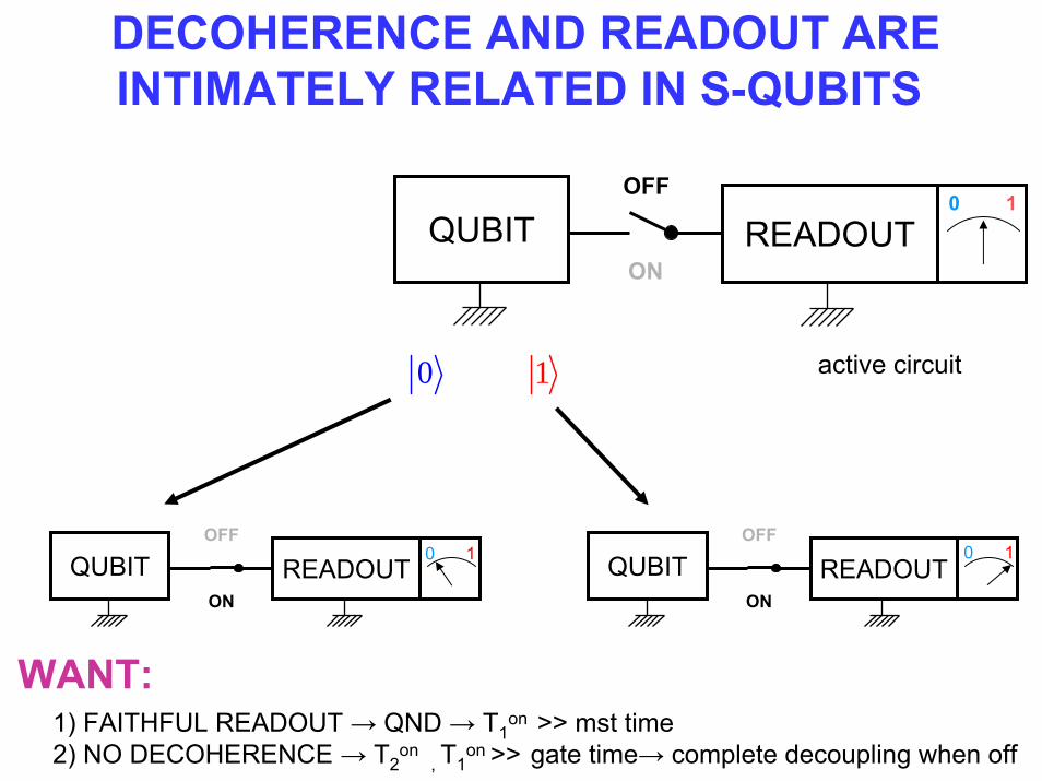
QUBIT READOUTON
OFF0 1
QUBIT READOUTOFF
ON
0 1 QUBIT READOUTOFF
ON
0 1
10
DECOHERENCE AND READOUT AREINTIMATELY RELATED IN S-QUBITS
active circuit
WANT:1) FAITHFUL READOUT → QND → T1
on >> mst time2) NO DECOHERENCE → T2
on , T1
on >> gate time→ complete decoupling when off

DISPERSIVE READOUT STRATEGY
rf signal in
01ω ω≠
QUBITCIRCUIT
0 1or

DISPERSIVE READOUT STRATEGY
rf signal in
or
rf signal out
QUBITCIRCUIT
QUBIT STATEENCODED IN PHASE
OF OUTGOING SIGNAL,NO ENERGY DISSIPATED
ON-CHIP0 1or

DISPERSIVE READOUT STRATEGY
rf signal in rf signal out
or
QUBITCIRCUIT
Important factors1) noise in detection2) phase shift per photon
0 1or
DO WITH ENOUGH PHOTONS TO GET1 CLASSICAL BIT OF INFORMATION

TWO KINDS OF DISPERSIVE READOUTS
"cQED" CIRCUIT:CAPACITIVE READOUTOFF-CHIP AMPLIFIER
in out
RESONATOR
"CBA" CIRCUIT:INDUCTIVE READOUT
IN-SITU AMPLIFICATION
outin
Exploit frequency shift of resonator coupled to qubit:readout off when resonator not driven

COMBINING SENSITIVITY & SPEED
NON-LINEAR OSCILLATORLINEAR OSCILLATOR
I. Siddiqi

COMBINING SENSITIVITY & SPEED01
01
NON-LINEAR OSCILLATORLINEAR OSCILLATOR(→ JBA-CBA)
not latching latching

COMBINING SENSITIVITY & SPEED01
01
NON-LINEAR OSCILLATORLINEAR OSCILLATOR
Q and preamp noisesets sensitivity
continuous, not latching projective, latching

COMBINING SENSITIVITY & SPEED01
01
NON-LINEAR OSCILLATORLINEAR OSCILLATOR
Q and preamp noisesets sensitivity
kT sets sensitivity !
continuous, not latching projective, latching

SOME REMARKS ONBIFURCATION READOUT

|0>
|1>
QUANTRONIUM IN MICROWAVE CAVITY
~ ADCIN OUT
AWG
40ns40ns200ns
t t
Metcalfe et al.Phys. Rev. B6174516 (2007)

QUANTRONIUM COMBINED WITHCAVITY BIFURCATION AMPLIFIER
Optical image3m
m
Output1
0
Input
Linear resonance frequency f0=9.64GHz, Quality factor: Q=160
10mm
readoutjunction
CPBSEM image

IMPLEMENTATIONS
Lumped-element parallel LC oscillator
(JBA)
Distributed element oscillator (CBA)
Coplanar waveguide
Coupled stripline
Parallel LC
(Limits Q-value)
Multiplexed readout and gate lines
Each resonator has different frequencyset by itslength

VARIATION: COUPLED STRIPLINE NON-LINEAR RESONATOR
Optical image of device
200µm
Gate
Slotline
SEM image of qubit
4µm
1. Completely fabricated using e-beam lithography2. Gate and readout lines separated3. Use differential mode in stripline for readout, common mode for gate
Advantages
Drawback: Purcell effect more difficult to control due to presence of common mode

CAVITY BIFURCATION : ANALOG OF OPTICALBISTABILITY
increasing the power in the cavity increases the readout coupling

CAVITY BIFURCATION : ANALOG OF OPTICALBISTABILITY
20 cav Jc
J P
L EnQ L ω
≈h
~100

Mapping Transition Frequency(with one readout tone only)
Monitor phase atfixed frequency in linear regime
Frequency (GHz)
Pha
se (D
eg)180
-180
9.649.59 9.69
0

Mapping Transition Frequency(with one readout tone only)
0 → 1Transitions:
0 → 2
ECP=17GHzEJ=15GHz

Mapping Transition Frequency(with one readout tone only)
0 → 1Transitions:
0 → 2
ECP=17GHzEJ=15GHz

Mapping Transition Frequency(with one readout tone only)
Bistable regime more gain
Gat
e ch
arge
(Coo
per p
airs
)
-1/2 Flux (flux quantum units)
1/2

Mapping Transition Frequency(with one readout tone only)
-1/2 Flux (flux quantum units)
1/2
Bistable regime more gain
Gat
e ch
arge
(Coo
per p
airs
)
0 → 1, 2Transitions, # photons
0 → 2, 30 → 2, 4

π pulse UrfMEASUREMENT OFREADOUT FIDELITY
Urf
Relaxationinduced byreadout
Unlike JBA,slope3 timestoo smallcomparedwith thy
TOO MANY READOUT PHOTONS?

Variability ofRamsey fringes
T2 = 500ns ± 300ns
Example fit of 5averaged traces~2sec acquisition time(resolution: 0.5MHz onf01 and 20ns on T2)
MHz repetition rateLarge SNR
NOISE SOURCE?

DISTRIBUTION OF RAMSEY DATAmethod A of van Harlingen et al. 2004
Lopsided frequency fluctuations
Charge noise amplitude1/f2
3( ) , 1.9 10gNS eαω α
ω−= :
value OK
(Karlsruhe)
EJ/EC = 3.6

DISTRIBUTION OF RAMSEY DATAvan Harlingen et al. 2004
Lopsided frequency fluctuations
Charge noise amplitude1/f2
3( ) , 1.9 10gNS eαω α
ω−=
value OK
(Karlsruhe)
Need larger EJ/EC

CONCLUSIONS OF THIS SECTIONON BIFURCATION READOUT
Speed and resolution of CBA has allowedus to measure charge fluctuations at
sweet spot of Cooper pair box in real timefor time scales of 1 second and up.
Our results confirm 1/f noise model of dephasing of Cooper pair box.
For EJ/EC~4 , sweet spot T2 limited bysecond order effects of charge noise
Must increase EJ/EC! TRANSMON

THE JOSEPHSON PARAMETRIC "CONVERTER":A QUANTUM-LIMITED
PRE-AMPLIFIER FOR QUBITDISPERSIVE READOUT
goal: provide high-gain, low noise amplifier for c-QED readoutrelationship with CBA: uses also non-linear on-chip Josephson element for gain, but no latching
outline: 1) Principle2) Implementation3) Preliminary data

CRYOELECTRONIC AMPLIFIERSAPPROACHING THE QUANTUM LIMIT
type EN/( ω/2) powergain
out-of-bandback-action
noise
easeof
use
HEMT 40-80 25-35dB small easy
SQUID 1-2 20-30dB concern OK
SET 1-2 15-20 dB concern OK
QPC 1 ~0dB very small difficult
HEMT: High Electron Mobility Transistor, SET: Single Electron Transistor, QPC: Quantum Point Contact

ARE THERE GENERAL GUIDING PRINCIPLESFOR CONSTRUCTING AN OPTIMAL AMPLIFIER?
CAN WE ACTUALLY BUILD ONE?
CAN WE DO A MEASUREMENT BEING ONLYLIMITED BY QUANTUM NOISE?
PIONEERING WORK BY Yurke et al. , 1986
RECENT THEORETICAL RESULTS BY Clerk, Girvin and Stone, 2004
principle of no wasted information

PARAMETRIC AMPLIFICATION PRINCIPLEIN THE SCATTERING LANGUAGE
Dispersive
Non-linear
Medium
ωpumpωpump
ωsignal ωsignal
ωidler ωidler(no signal)
FUNDAMENTAL EQUATION :
0 mod idlersig pnal umpω ωω + =

MASER/LASER
pumpωsignalω
pumpωsignalω
pumpωsignalω
idlerω
signal inMANY SYSTEMS
WITH FEW LEVELS:ATOMS,
MOLECULES, ETC
idlerω
pumpωsignalω SIGNAL OUT
DIFFICULT TO IMPLEMENTAT RF FREQUENCIES however see recent NEC results on single atom circuit maser

PREFER TO USE 1 NON-LINEAR DEGREE OF FREEDOM WITH MANY ENERGY LEVELS
CONTROLIS EASIERPotential energy
Position coordinate
Cj
2
20
11 ...4J
IL
I
⎛ ⎞⎜ ⎟+ +⎜ ⎟⎝ ⎠
in practice,of order 102-3
levels

TOWARDS THE PUREST NON-LINEARITY: THE
JOSEPHSONRING MODULATOR
4 modes:

SCHEMATICS OF JOSEPHSON AMPLIFIERBASED ON RING MODULATOR
SIGNAL (ω1)
IDLER (ω2)
Φ=Φ0/2
PUMP (Ω)

WHY THIS SYMMETRY?
-1
0
1
E/4E
J
0Φ
a
b
Φ0
4 states 4Φ0-periodic states
φa + φb + φc + φd =2πΦΦ0
sinφa = sinφb = sinφc = sinφd
satisfy
At Φ=Φ0/2 and for small X,Y,Z
Ering = α XYZ −X 2
4−
Y 2
4−
Z 2
2⎡
⎣ ⎢
⎤
⎦ ⎥
Mix 3 orthogonal
modes X, Y and ZSpurious terms renormalize
the mode frequencies(Steve Girvin)
Isolates useful non-linearity with minimal number of spurious terms

ACTUALIMPLEMEN-TATION OFJOSEPHSON
PARAMETRICAMPLIFIER
SIGNAL
IDLER
180ºhybridcoupler
Design goals:TN < hf/kBGain > 20 dBBandwidth > 5 MHzDynamic range > 20 dB chip
Φ0/2

MICROGRAPH OF JOSEPHSON SUPERCONDUCTING CIRCUIT
6.2 GHz
100µm
500 nmPump1.6 GHz

CHIP DESIGN: MEANDER COPLANARSTRIPLINE RESONATORS
6.2 GHz
1.6 GHz
Pump @ 7.8 GHz
5 mm

MEASUREMENT SETUP
JPCChip
Pump line LF lineHF lineIn In
300mK
1K
4K
300K OutOut
-20 dB
50 Ω 50 Ω
+28 dB
-20 dB
-30 dB
-20 dB
-20 dB
-30 dB
50 Ω 50 Ω
+50dB +50dB

LOCATINGTHE HALF
FLUX-QUANTUMWORKING
POINT
color: phase of reflected signal

PRELIMINARY DATA: MEASUREMENTOF REFLECTED SIGNAL
42dB
30dB
No pump
With pump

PRELIMINARY DATA: DYNAMIC RANGE

CONCLUSIONS AND PERSPECTIVES
We have built a ultra-low noise practical microwaveamplifier operating in the quantum regime
Construction is simpler than the microstrip SQUID
Noise should be only limited by quantum fluctuations
Measurement of noise temperature is in progress
This amplifier is useful for:- minimally invasive readout of solid-state qubits- metrology of ampere (detection of Bloch osc.)- detection of very weak signals in astrophysics

TWO CASES
3 1 212 2
1 2
2 ;1
Q QG
χτ ττ ω ω
= =−
12 2
21
G ττ
=+

SPECTROSCOPYReadoutSpectroscopy pulse
Varying frequency
Fit:
Ecp = 17.0GHz
EJ0 = 15.02GHz

RELAXATION TIME, T1
Readoutπ pulse tw
T1=1.4µs↔1.8µs

RAMSEY FRINGESReadoutπ/2 pulse ∆t π/2 pulse
200ns ≤ T2 ≤ 800ns, ∆t
4 401 22 2.10 7.10Q Tϕ πν= = ↔
49

QUANTRONIUM IN MICROWAVE CAVITY
OFF-RESONANCE NMR-TYPEPULSE SEQUENCE
FOR QUBIT MANIPULATION
50

QUANTRONIUM IN MICROWAVE CAVITY
|0>
|1>
READOUTPROBING
PULSEor
~ ADCIN OUT

|0>
|1>
QUANTRONIUM IN MICROWAVE CAVITY
~ ADCIN OUT
AWG
40ns40ns200ns

IMPLEMENTATIONS
Lumped-element parallel LC oscillator
(JBA)
Distributed element oscillator (CBA)
53
Coplanar waveguide
Coplanar stripline
Parallel LC
(Limits Q-value)
Multiplexed readout and gate lines
Each resonator has different frequencyset by itslength

THIS YEAR: COUPLED STRIPLINE NON-LINEAR RESONATOR
Optical image of device
200µm
Gate
Slotline
SEM image of qubit
4µm
Advantages: 1. Completely fabricated using e-beam lithography2. Gate and readout lines separated
3. Excite ± mode in slotline for readout54

CAVITY BIFURCATION : ANALOG OF OPTICALBISTABILITY
increasing the power in the cavity increases the readout coupling

CBA WITH QUANTRONIUMOptical image
Output3m
m
56
10mm
readoutjunction
CPB
1
0
Input
Linear resonance frequency f0=9.64GHzQuality factor: Q=160
SEM image

OBSERVATION OF BISTABILITY
τm = 2µs
2µs 3µs 10ns
counts
Im[V
out]
Re[Vout]
57

OBSERVATION OF BISTABILITY
2µs 3µs 10ns
counts
Im[V
out]
Re[Vout]
58

OBSERVATION OF BISTABILITY
2µs 3µs 10ns
counts
Im[V
out]
Re[Vout]
59

OBSERVATION OF BISTABILITY
2µs 3µs 10ns
counts
Drive amplitude variesonly by 1% thru
bifurcation!
Im[V
out]
Re[Vout]
60

OBSERVATION OF BISTABILITY
2µs 3µs 10ns
counts
Im[V
out]
QUBIT STATEENCODED IN COMPLEX
AMPLITUDEOF TRANSMITTED PULSE
Re[Vout]
61

HYSTERESIS → LATCHING
0
1
Ω/2π = 4.2GHzT=15mK
1 ms sweep
62

Urf
14.3 GHz
9.5 GHz
πMEASUREMENT OFREADOUT FIDELITY
Urf
63

Urf
14.3 GHz
9.5 GHz
πMEASUREMENT OFREADOUT FIDELITY
Urf
relaxation
slope3 timestoo small
64

65
Urf
14.3 GHz
9.5 GHz
πMEASUREMENT OFREADOUT FIDELITY
Urf
F 0
1
10 011 p pF = − −F = 45−61%
on 4 samples
Readout relaxation Reduced contrast

THE AMPLIFIER: THE PHYSICIST’S BASIC TOOL, FROM ASTROPHYSICS TO NANOPHYSICS
RADIO-FREQUENCYPHENOMENON
(MHz-GHz)
DATA RECORD
AMPLI-FIER DETERtic
SIGNALDeterministic signal
++
+
THERMALNOISEThermal noise
ADDEDNOISE

ALTHOUGH NECESSARY, THE AMPLIFIERALWAYS DEGRADES INFORMATION
DET. SIGNAL
+
+
TH. NOISE
ADDEDNOISE
BACKGROUND NOISEAT RECORD LEVEL
>>

ALTHOUGH NECESSARY, THE AMPLIFIERALWAYS DEGRADES INFORMATION
DET. SIGNAL
+
+
TH. NOISE
ADDEDNOISE
BACKGROUND NOISEAT RECORD LEVEL
>>
TH. NOISE<1EFFICIENCY =
TH. NOISE + ADDED NOISE
Statistical Mechanics Information Theory

ALTHOUGH NECESSARY, THE AMPLIFIERALWAYS DEGRADES INFORMATION
DET. SIGNAL
+
+
TH. NOISE
ADDEDNOISE
BACKGROUND NOISEAT RECORD LEVEL
>>
QUANTUM REGIME:ENERGY OF EACH MODE OF
SIGNAL AND THERMAL NOISEIS OF ORDER 1 PHOTON
QUANTUM LIMIT:kBT / ω → 0
TH. NOISE → Z.P. FLUCT.
TH. NOISEEFFICIENCY =
TH. NOISE + ADDED NOISE
Statistical Mechanics Information Theory

WHAT IS A TEMPORAL MODE OF A SIGNAL?
mwpick “window” wavepacket
time
p pω ω= ∆
( ) 1ω −∆
nt n t= ∆
( )1/ 2ω∆
( ),m n p=window index:
2t ω π∆ ⋅ ∆ =
( ) ( )' ' '| dm m m m m mw w w t w t t δ+∞ ∗
−∞= =∫orthonormality:
frequency t∆
ω∆p
n time
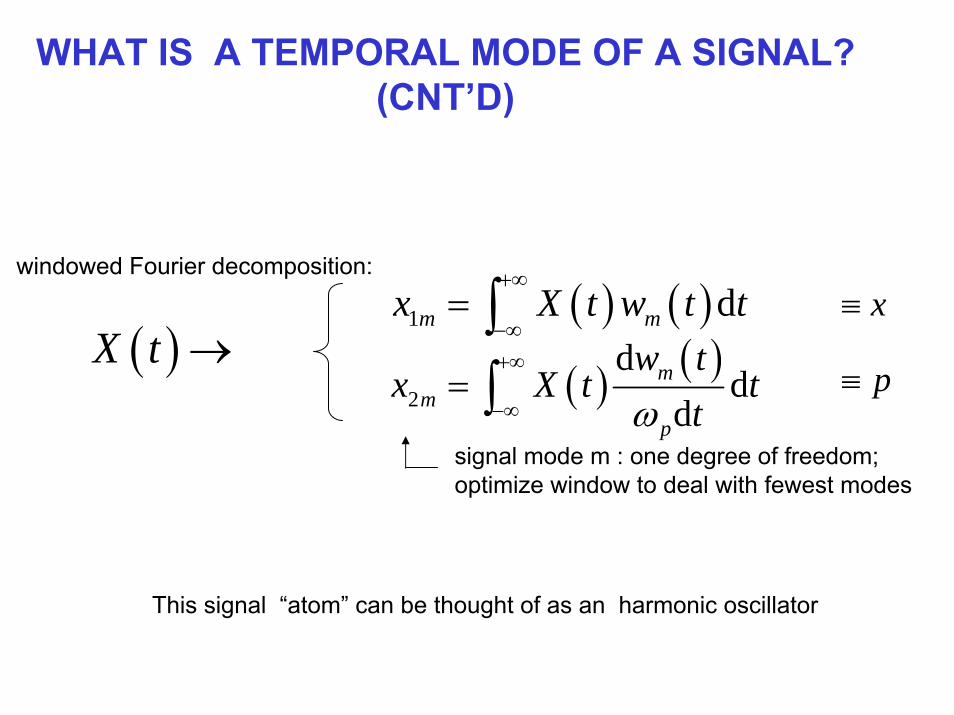
WHAT IS A TEMPORAL MODE OF A SIGNAL? (CNT’D)
windowed Fourier decomposition:
( ) ( )1 dm mx X t w t t+∞
−∞= ∫
signal mode m : one degree of freedom;optimize window to deal with fewest modes
x≡
p≡( )X t →
( ) ( )2
dd
dm
mp
w tx X t t
tω+∞
−∞= ∫
This signal “atom” can be thought of as an harmonic oscillator

GEOMETRIC REPRESENTATIONOF A SIGNAL MODE
x2
x1α
E noise fuzzdisc
E = signal mode energyα = signal mode phase

AMPLIFICATION OF A QUANTUM SIGNAL
IN OUT
x2
x1
x2
x1
2FG ωh
α
GE2ωh
α
E

AMPLIFICATION AT THE QUANTUM LIMIT
IN OUT
x2
x1
x2
2ωh
α
E
x1
G ωh
α
GE Fmin=2

AMPLIFICATION AT THE QUANTUM LIMIT
IN OUT
x2
x1
x2
2ωh
α
E
x1
G ωh
α
GE
THE AMPLIFIER ADDS ONLYANOTHER ½ PHOTON !
(Caves, 1982)

NON-LINEAR AMPLIFICATION OF READOUT SIGNAL
Vd
Vdrive
R
C
L
Non-linear LC oscillator
w
|Vou
t|
linear LC oscillator
V
LJ
Vd

NON-LINEAR AMPLIFICATION OF READOUT SIGNAL
Vd
R
C
L
Non-linear LC oscillator
|Vou
t|
Vd
stable
unstable
stable
LJ

NON-LINEAR AMPLIFICATION OF READOUT SIGNAL
Vd
R
C
L
Non-linear LC oscillator
Quantronium Qubit0
1
E/E
c
Energy levels
Cg
Vg
g gC V e
0
1
2
|Vou
t|
Vd
stable
unstable
stable
LJ

NON-LINEAR AMPLIFICATION OF READOUT SIGNAL
Vd
R
C
L
Non-linear LC oscillator
Quantronium Qubit0
1
E/E
c
Energy levels
Cg
Vg
g gC V e
0
1
2
|Vou
t|
Vd
stable
unstable
stable
LJ
Mapping
0
1

RF READOUT OF "QUANTRONIUM" BASED ON BIFURCATION AMPLIFIER (JBA)
Cooper pairbox qubit
U
CHARGE PORT:CONTROL
PHASE PORT: READOUT
junction for non-linearinductance probing (gain)
shunting capacitors
(lowers frequency)

RF READOUT OF "QUANTRONIUM" BASED ON BIFURCATION AMPLIFIER (JBA)
Cooper pairbox qubitQUBIT CONTROL
PULSE SEQUENCE
U

RF READOUT OF "QUANTRONIUM" BASED ON BIFURCATION AMPLIFIER (JBA)
U
Cooper pairbox qubit READOUT
PROBINGRF PULSE

RF READOUT OF "QUANTRONIUM" BASED ON BIFURCATION AMPLIFIER (JBA)
Cooper pairbox qubit
U
QUBITSTATE
ENCODEDIN REFL.PULSEPHASE
|0>
|1>
obeys the "no energyleft behind" principle!

QUANTUM OPTICS WITH CIRCUIT ELEMENTS
( )i t
[ ],Z X
Yiσ σ
σ=†,
1
a a⎡ ⎤⎣ ⎦=
STEER READOUT
( )u t
( )
( ) ( ) ( )( )0
† †4†
1
1
X Z
P Z
u t
a a a a t a
H
ai
ω
ω λ
σ
µ
σ
σ
= −
+ + + −+ +
h
h
4
48
JRJ
RC
EE
E
λ
µ
=
=
( ) ( )
( ) ( )2
g
P
Cu t e U t
C
i t I tCω
Σ
=
=h
can alsobe a cavity mode
(CBA, E. Boaknin et al.)
a

PROBLEM: DIFFICULT TO MAKEGOOD CAPACITORS AT HIGH
FREQUENCIES

SOLUTION: USE CAVITY RESONATOR
"Cavity Bifurcation Amplifier" configuration
very similar, but different from:
"circuit-QED" configuration
analogous to cavity QED expts byHaroche, Raimond, Brune et al.

LONG TERM GOAL: SCALABLE ARCHITECTURE
Cooper-pair box charge qubits
superconductingtransmission-line cavity
as quantum bus
multiplexed cavity Josephson bifurcation amplifiers for
readout of individual qubits
frequency-selectiveRF pulses for
1 and 2-bit operations
module scalable to 10’s of qubits if coherence and fidelity allow(need two superconducting wiring layers and one dielectric isolation layer)

SUPERCONDUCTING CAVITY = FABRY-PEROT
3mm
10mm
100µm
Nb
f = 2,5,10GHz

10µm
CPW ground
ISLAND
Readout junction
CPW ground
SAMPLE OF QUANTRONIUM IN CAVITY

QUANTRONIUM: AN ARTIFICIAL ATOM
Φ
U ΦgC
island
U
orthogonalityof steer andread modes
readsteer
IVion et al. 2002

RF READOUT OF "QUANTRONIUM" BASED ON BIFURCATION AMPLIFIER (JBA)
( )i t
( )u tSTEER
Cooper pairbox qubit READOUT
PROBINGRF PULSE
READOUT
|0>
|1>
QUBIT STATEENCODED IN
REFLECTED PULSEPHASE

RF READOUT OF "QUANTRONIUM" BASED ON BIFURCATION AMPLIFIER (JBA)
( )i t
( )u tSTEER
Cooper pairbox qubit READOUT
PROBINGRF PULSE
READOUT

QUANTRONIUM IN CAVITY:CAVITY BIFURCATION READOUT (CBA)
Udc
qubit
Urf
photon

CAVITY BIFURCATION : ANALOG OF OPTICALBISTABILITY
increasing the power in the cavity increases the readout coupling

-10
-5
0
5
10
V / V
d
5 4 3 2 1
ωd − ω0 / Γ
Log
P/P
c(d
B)
bifurcation critical parametersagree very well with thy
(ωd - ω0) / Γ

OBSERVATION OF BISTABILITY
τm = 2µs
2µs 3µs 10ns
counts
Im[V
out]
Re[Vout]

OBSERVATION OF BISTABILITY
2µs 3µs 10ns
counts
Im[V
out]
Re[Vout]

OBSERVATION OF BISTABILITY
2µs 3µs 10ns
counts
Im[V
out]
Re[Vout]

OBSERVATION OF BISTABILITY
2µs 3µs 10ns
counts
amplitude variesonly by 1% thru
bifurcation!
Im[V
out]
Re[Vout]

OBSERVATION OF BISTABILITY
2µs 3µs 10ns
counts
Im[V
out]
QUBIT STATEENCODED IN COMPLEX
AMPLITUDEOF TRANSMITTED PULSE
Re[Vout]

HYSTERESIS → LATCHING
0
1
Ω/2π = 4.2GHzT=15mK
1 ms sweep

Urf
14.3 GHz
9.5 GHz
πMEASUREMENT OFREADOUT FIDELITY
Urf

Urf
14.3 GHz
9.5 GHz
πMEASUREMENT OFREADOUT FIDELITY
Urf
relaxation
slope3 timestoo small

Urf
14.3 GHz
9.5 GHz
πMEASUREMENT OFREADOUT FIDELITY
Urf
F 0
1
10 011 p pF = − −F = 45−61%
on 4 samples
Readout relaxation Reduced contrast

CAVITY QUANTRONIUMRABI OSCILLATIONS
M. Metcalfe et al.
f = 14.3GHz

20%
40%
60%
acqu
isiti
on ti
me
(s)
RAMSEYFRINGES
T2 =500ns+-
200ns
what is this dirt?- unpaired electrons- vortex motion- "glassy" two-levels

preparationpulse
analysis pulse
h φTOMOGRAPHY
exp
h φ
thy
0 0 12
+ 0 12− 01
Initial states

MULTIPLEXED CAVITY JBA's
IDEA: N QUBITS READ BY AN ARRAY OF MULTIPLEXEDRESONATORS (HARP PRINCIPLE)
2 mm 2 mm
Goal: frequency domain “MUX” of qubit readouts

MEASUREMENT OF MULTIPLE BIFURCATION

WHY IS IT IMPORTANT TO APPROACHTHE QUANTUM LIMIT OF AMPLIFICATION
AT MICROWAVE FREQUENCIES?
S
NOISE ENERGYIGNAL ENE BANDY HRG WIDT×INFORMATION CAPACITY =
(weak signal limit)
(Shannon 1948)
CAVEAT: WE WANT ALSO MAXIMUM POWER GAIN, QUIETNESS, EASE OF OPERATION, ETC.....

ARE THERE GENERAL GUIDING PRINCIPLESFOR CONSTRUCTING AN OPTIMAL AMPLIFIER?
CAN WE ACTUALLY BUILD ONE?
CAN WE DO A MEASUREMENT BEING ONLYLIMITED BY QUANTUM NOISE?
PIONEERING WORK BY Yurke et al. , 1986
RECENT THEORETICAL RESULTS BY Clerk, Girvin and Stone, 2004