Embed Size (px)
Citation preview
rfRXD0420/0920
UHF ASK/FSK/FM Receiver
Features:
• Low cost single conversion superheterodyne
receiver architecture
• Compatible with rfPIC™ and rfHCS series of RF
transmitters
• Easy interface to PICmicro® microcontroller
(MCU) and KEELOQ® decoders
• VCO phase locked to quartz crystal reference:
- Narrow receiver bandwidth
- Maximizes range and interference immunity
• Selectable LNA gain control for improved dynamic
range
• Selectable IF bandwidth via external ceramic IF
filter
• Received Signal Strength Indicator (RSSI) for
signal strength indication (FSK, FM) and ASK
demodulation
• FSK/FM quadrature (phase coincidence) detector
demodulator
• 32-Lead LQFP package
UHF ASK/FSK Receiver:
• Single frequency receiver set by crystal frequency
• Receive frequency range:
• Maximum data rate:
- ASK: 80 Kbps NRZ
- FSK: 40 Kbps NRZ
• IF frequency range: 455 kHz to 21.4 MHz
• RSSI range: 70 dB
• Frequency deviation range: ±5 kHz to ±120 kHz
• Maximum FM modulation frequency: 15 kHz
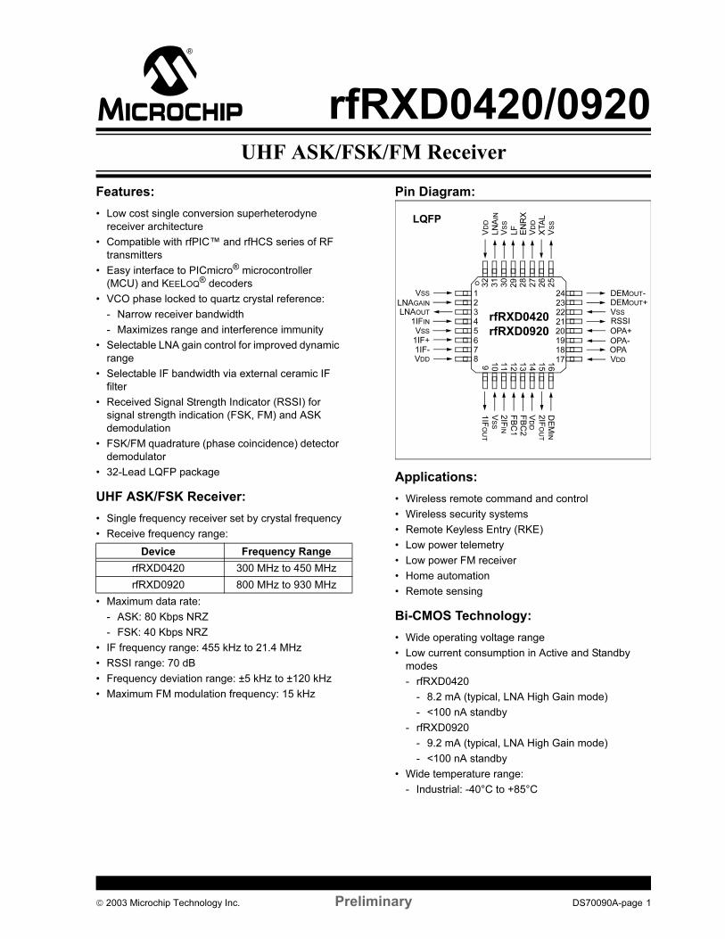
Pin Diagram:
Applications:
• Wireless remote command and control
• Wireless security systems
• Remote Keyless Entry (RKE)
• Low power telemetry
• Low power FM receiver
• Home automation
• Remote sensing
Bi-CMOS Technology:
• Wide operating voltage range
• Low current consumption in Active and Standby
modes
- rfRXD0420
- 8.2 mA (typical, LNA High Gain mode)
- <100 nA standby
- rfRXD0920
- 9.2 mA (typical, LNA High Gain mode)
- <100 nA standby
• Wide temperature range:
- Industrial: -40°C to +85°C
Device Frequency Range
rfRXD0420 300 MHz to 450 MHz
rfRXD0920 800 MHz to 930 MHz
2
3
4
5
6
1
15
169
10
11
12
29
8
7
32
31
30
13
14
23
24
17
18
19
20
21
22
27
25
26
28
DEM
IN
2IF
OUT
1IF
OUT
VDD
FBC2
FBC1
2IF
IN
VSS
VDD
LNAIN
VSS
LF
ENRX
VDD
XTAL
VSS
DEMOUT-
DEMOUT+
VSS
RSSI
OPA+
OPA-
OPA
VDD
VSS
LNAGAIN
LNAOUT
1IFIN
VSS
1IF+
1IF-
VDD
rfRXD0420
LQFP
rfRXD0920
2003 Microchip Technology Inc. Preliminary DS70090A-page 1
rfRXD0420/0920
1.0 DEVICE OVERVIEW
The rfRXD0420/0920 are low cost, compact single
frequency short-range radio receivers requiring only a
minimum number of external components for a
complete receiver system. The rfRXD0420 covers the
receive frequency range of 300 MHz to 450 MHz and
the rfRXD0920 covers 800 MHz to 930 MHz. The
rfRXD0420 and rfRXD0920 share a common architec-
ture. They can be configured for Amplitude Shift Keying
(ASK), Frequency Shift Keying (FSK), or FM modula-
tion. The rfRXD0420/0920 are compatible with rfPIC™
and rfHCS series of RF transmitters.
• High frequency stability over temperature and
power supply variations
• Low spurious signal emission
• High large-signal handling capability with
selectable LNA gain control for improved dynamic
range
• Selectable IF bandwidth via external low cost
ceramic IF filter. The IF Frequency range is
selectable between 455 kHz to 21.4 MHz. This
facilitates the use of readily available low cost
10.7 MHz ceramic IF filters in a variety of
bandwidths.
• ASK or FSK for digital data reception
• FM modulation for analog signal reception
• FSK/FM demodulation using quadrature detector
(phase coincidence detector)
• Received Signal Strength Indication (RSSI) for
signal strength indication and ASK detection
• Wide supply voltage range
• Low active current consumption
• Very low standby current
The rfRXD0420/0920 is a single conversion superhet-
erodyne architecture. A block diagram is illustrated in
Figure 1-1. The rfRXD0420/0920 consists of:
• Low-noise amplifier (LNA) - Gain selectable
• Mixer for down-conversion of the RF signal to the
Intermediate Frequency (IF) followed by an IF
preamplifier
• Fully integrated Phase-Locked Loop (PLL)
frequency synthesizer for generation of the Local
Oscillator (LO) signal. The frequency synthesizer
consists of:
- Crystal oscillator
- Phase-frequency detector and charge pump
- High-frequency Voltage Controlled Oscillator
(VCO)
- Fixed feedback divider
- rfRXD0420 = divide by 16
- rfRXD0920 = divide by 32
• IF limiting amplifier to amplify and limit the IF
signal and for Received Signal Strength Indication
(RSSI) generation
• Demodulator (DEMOD) section consists of a
phase detector (MIXER2) and amplifier creating a
quadrature detector (also known as a phase
coincidence detector) to demodulate the IF signal
in FSK and FM modulation applications
• Operational amplifier (OPA) that can be config-
ured as a comparator for ASK or FSK data
decision or as a filter for FM modulation.
• Bias circuitry for bandgap biasing and circuit
shutdown
DS70090A-page 2 Preliminary 2003 Microchip Technology Inc.

rfRXD0420/0920
FIGURE 1-1: rfRXD0420/0920 BLOCK DIAGRAM
LN
ALN
A
LNA
1IF
31
34
1IF+
1IF-
76
911
12
13
21
1IF
2IF
FBC1
FBC2
RS
SI
20
19
18
OP
A+
OP
A-
OPA
XTAL
LF
29
26
Bia
s
ENRX
28
LNA
2
OP
A
16
15
2IF
DEM +--
+-
OUT+
OUT-
24
23D
EM
OD
IN
OUT
IN
OUT
IN
GAIN
OUT
IN
VSS
1
VSS
5
VDD
8
VSS
10
VDD
14
VDD
17
VD
D
32
VS
S
30
27
VDD
25
VSS
DEM
DEM
MIX
ER
1IF
Pre
am
p
IF L
imitin
g A
mplif
ier
MIXER2
22
VSS
with R
SS
I
Cry
sta
l
Oscill
ato
r
Phase D
ete
cto
r
and
Charg
e P
um
p
Voltage
Contr
olle
dO
scill
ato
r
Fix
ed D
ivid
e b
yF
requency
Synth
esiz
er
16: rf
RX
D0420
32: rf
RX
D0920
2003 Microchip Technology Inc. Preliminary DS70090A-page 3
rfRXD0420/0920
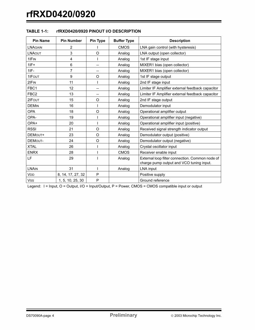
TABLE 1-1: rfRXD0420/0920 PINOUT I/O DESCRIPTION
Pin Name Pin Number Pin Type Buffer Type Description
LNAGAIN 2 I CMOS LNA gain control (with hysteresis)
LNAOUT 3 O Analog LNA output (open collector)
1IFIN 4 I Analog 1st IF stage input
1IF+ 6 -- Analog MIXER1 bias (open collector)
1IF- 7 -- Analog MIXER1 bias (open collector)
1IFOUT 9 O Analog 1st IF stage output
2IFIN 11 I Analog 2nd IF stage input
FBC1 12 -- Analog Limiter IF Amplifier external feedback capacitor
FBC2 13 -- Analog Limiter IF Amplifier external feedback capacitor
2IFOUT 15 O Analog 2nd IF stage output
DEMIN 16 I Analog Demodulator input
OPA 18 O Analog Operational amplifier output
OPA- 19 I Analog Operational amplifier input (negative)
OPA+ 20 I Analog Operational amplifier input (positive)
RSSI 21 O Analog Received signal strength indicator output
DEMOUT+ 23 O Analog Demodulator output (positive)
DEMOUT- 24 O Analog Demodulator output (negative)
XTAL 26 I Analog Crystal oscillator input
ENRX 28 I CMOS Receiver enable input
LF 29 I Analog External loop filter connection. Common node of
charge pump output and VCO tuning input.
LNAIN 31 I Analog LNA input
VDD 8, 14, 17, 27, 32 P Positive supply
VSS 1, 5, 10, 25, 30 P Ground reference
Legend: I = Input, O = Output, I/O = Input/Output, P = Power, CMOS = CMOS compatible input or output
DS70090A-page 4 Preliminary 2003 Microchip Technology Inc.

rfRXD0420/0920
2.0 CIRCUIT DESCRIPTION
This section gives a circuit description of the internal
circuitry of the rfRXD0420/0920 receiver. External
connections and components are given in the
APPLICATION CIRCUITS section.
2.1 Bias Circuitry
Bias circuitry provides bandgap biasing and circuit
shutdown capabilities. The ENRX (Pin 28) modes are
summarized in Table 2-1. The ENRX pin is a CMOS
compatible input and is internally pulled down to Vss.
2.2 Frequency Synthesizer
The Phase-locked Loop (PLL) frequency synthesizer
generates the Local Oscillator (LO) signal. It consists
of:
• Crystal oscillator
• Phase-frequency detector and charge pump
• Voltage Controlled Oscillator (VCO)
• Fixed feedback divider:
- rfRXD0420 = divide by 16
- rfRXD0920 = divide by 32
2.2.1 CRYSTAL OSCILLATOR
The internal crystal oscillator is a Colpitts type oscilla-
tor. It provides the reference frequency to the PLL. A
crystal is normally connected to the XTAL (Pin 26) and
ground. The internal capacitance of the crystal oscilla-
tor is 15 pF. Alternatively, a signal can be injected into
the XTAL pin from a signal source. The signal should
be AC coupled via a series capacitor at a level of
approximately 600 mVpp.
The XTAL pin is illustrated in Figure 2-1.
FIGURE 2-1: BLOCK DIAGRAM OF
XTAL PIN
The PLL consists of a phase-frequency detector,
charge pump, voltage-controlled oscillator (VCO), and
fixed divide-by-16 (rfRXD0420) or divide-by-32
(rfRXD0920) divider. The rfRXD0420/0920 employs a
charge pump PLL that offers many advantages over
the classical voltage phase detector PLL: infinite pull-in
range and zero steady state phase error. The charge
pump PLL allows the use of passive loop filters that are
lower cost and minimize noise. Charge pump PLLs
have reduced flicker noise thus limiting phase noise.
An external loop filter is connected to pin LF (Pin 29).
The loop filter controls the dynamic behavior of the
PLL, primarily lock time and spur levels. The applica-
tion determines the loop filter requirements.
The VCO gain for the rfRXD0420/0920 receivers are
listed in Table 2-2.
The LF pin is illustrated in Figure 2-2.
FIGURE 2-2: BLOCK DIAGRAM OF LOOP
FILTER PIN
2.3 Low Noise Amplifier
The Low-Noise Amplifier (LNA) is a high-gain amplifier
whose primary purpose is to lower the overall noise
figure of the entire receiver thus enhancing the receiver
sensitivity. The LNA is an open-collector cascode
design. The benefits of a cascode design are:
• high gain with low noise
• high-frequency
• wide bandwidth
• low effective input capacitance with stable input
impedance
• high output resistance
• high reverse isolation that provides improved
stability and reduces LO leakage
TABLE 2-1: BIAS CIRCUITRY CONTROL
ENRX(1) Description
0 Standby mode
1 Receiver enabled
Note 1: ENRX has internal pull-down to Vss
XTAL
26
40 µAVSS
VSS VSS
30 pF
30 pF
50 kΩVDD VDD
VDD
TABLE 2-2: PLL PARAMETERS
Device KVCO(1) ICP(1) Divider
rfRXD0420 250 MHz/V at
433 MHz
60 µA 16
rfRXD0920 300 MHz/V at
868 MHz
60 µA 32
Note 1: Typical value
LF
29
VSS
VSS
VSS
4 pF
200 Ω
400 Ω
VDD
2003 Microchip Technology Inc. Preliminary DS70090A-page 5

rfRXD0420/0920
Approximate LNA noise figures are listed in Table 2-3.
LNAIN (Pin 31) has an input impedance of approxi-
mately 26 Ω || 2 pF single-ended.
LNAOUT (Pin 3) has an open-collector output and is
pulled up to VDD via a tuned circuit.
Important: To ensure LNA stability the VSS pin (Pin 1)
must be connected to a low impedance ground.
The LNA pins are illustrated in Figure 2-3.
FIGURE 2-3: BLOCK DIAGRAM OF LNA
PINS
The gain of the LNA can be selected between High and
Low Gain modes by the LNAGAIN pin (Pin 2). LNAGAIN
is a CMOS input with hysteresis. Table 2-4 summarizes
the voltage levels and modes for LNA gain.
In the High Gain mode the LNA operates normally. In
Low Gain mode the gain of the LNA is reduced approx-
imately 25 dB, reduces total supply current, and
increases maximum input signal levels (see Electrical
Characteristics section for values).
2.4 MIXER1 and IF Preamp
MIXER1 performs down-conversion of the RF signal to
the Intermediate Frequency (IF) and is followed by an
IF preamplifier.
1IFIN (Pin 4) has an approximately 33 Ω single-ended
input impedance. The 1IFIN pin is illustrated in Figure 2-
4.
The 1IF+ (Pin 6) and 1IF- (Pin 7) are bias connections
to the MIXER1 balanced collectors. Both pins are
open-collector outputs and are individually pulled up to
VDD by a load resistor. The MIXER1 bias pins are illus-
trated in Figure 2-5.
1IFOUT (Pin 9) has an approximately 330 Ω single-
ended output impedance. The 330 Ω impedance
provides a direct match to low cost ceramic IF filters.
The 1IFOUT pins is illustrated in Figure 2-6.
FIGURE 2-4: BLOCK DIAGRAM OF MIXER1
PIN
FIGURE 2-5: BLOCK DIAGRAM OF MIXER1
BIAS PINS
FIGURE 2-6: BLOCK DIAGRAM OF IF
PREAMP PIN
2.5 IF Limiting Amplifier with RSSI
The IF Limiting Amplifier amplifies and limits the IF
signal at the 2IFIN pin (Pin 11). It also generates the
Received Signal Strength Indicator (RSSI) signal
(Pin 21).
2.5.1 IF LIMITING AMPLIFIER
Magnitude control circuitry is used in the last stage of
the receiver to keep the signal constant for demodula-
tion. It can consist of a limiting or Automatic Gain
Control (AGC) amplifier. A limiting amplifier is
TABLE 2-3: LNA NOISE FIGURES
Device Noise Figure(1)
rfRXD0420 TBD
rfRXD0920 TBD
Note 1: Approximate value
TABLE 2-4: LNA GAIN CONTROL
LNAGAIN Description
< 0.8 V High Gain mode
> 1.4 V Low Gain mode
LNA
LNA
31
3
IN
OUT
VSS
1VSS
VSS
VSS
5 kΩVDD
0.8V
1.6V
VDD
1IF
4
IN
VSS
VSS
13 Ω
13 Ω
VDD
500 µA
1IF+
6
500 µA
1IF-
7
500 µA
VSS
VSS
VSS
VSS
20 pF 20 pF
VDD VDD
1IF
9
OUT
230 µA
VSSVSS
130 Ω
6.8 kΩVDD
VDD VDD
DS70090A-page 6 Preliminary 2003 Microchip Technology Inc.

rfRXD0420/0920
employed in this design because it can handle a larger
dynamic range while consuming less power with simple
circuitry than AGC circuitry.
The internal resistance of the 2IFIN pin is approximately
2.2 kΩ. In order to terminate ceramic IF filters whose
output impedance is 330 Ω, a 390 Ω resistor can be
paralleled to the 2IFIN and FBC2 pins.
FBC1 (Pin 12) and FBC2 (Pin 13) are connected to
external feedback capacitors.
The IF Limiting Amplifier pins are illustrated in
Figures 2-7 and 2-8.
FIGURE 2-7: BLOCK DIAGRAM OF IF
LIMITING AMPLIFIER INPUT
PINS
FIGURE 2-8: BLOCK DIAGRAM OF IF
LIMITING AMPLIFIER OUTPUT
PIN
2.5.2 RECEIVED SIGNAL STRENGTH
INDICATOR (RSSI)
The RSSI signal is proportional to the log of the signal
at 2IFIN. The 2IFIN input RSSI range is approximately
40 µV to 160 mV. The slope of the RSSI output is
approximately 26 mV/dB of RF signal.
The RSSI output has an internal 36 kΩ resister to Vss
fed by a current source. This resistor converts the
RSSI current to voltage.
For Amplitude Shift Keying (ASK) demodulation, RSSI
is compared to a reference voltage (static or dynamic).
Post detector filtering is easily implemented by
connecting a capacitor to ground from the RSSI pin
effectively creating an RC filter with the internal 36 kΩ
resistor.
For FSK and FM demodulation, the RSSI represents
the received signal strength of the incoming RF signal.
The RSSI pin is illustrated in Figure 2-9.
FIGURE 2-9: BLOCK DIAGRAM OF RSSI
PIN
2.6 Demodulator
The demodulator (DEMOD) section consists of a phase
detector (MIXER2) and amplifier creating a quadrature
detector (also known as a phase coincidence detector)
to demodulate the IF signal in FSK and FM modulation
applications. The quadrature detector provides all the
IF functions required for FSK and FM demodulation
with only a few external parts.
The in-phase signal comes directly from the output of
the IF limiting amplifier to MIXER2. The quadrature
signal is created by an external tuned circuit from the
output of the IF limiting amplifier (2IFOUT, Pin 15) AC-
coupled to the MIXER2 DEMIN (Pin 16) input. The input
impedance of the DEMIN pin is approximately 47 kΩ.
The external tuned circuit can be constructed from sim-
ple inductor-capacitor (LC) components but will require
one of the elements to be tunable. A no-tune solution
can be constructed with a ceramic discriminator.
The output voltage of the DEMOD amplifier (DEMout+
and DEMout-, Pins 23 and 24) depends on the peak
deviation of the FSK or FM signal and the Q of the
external tuned circuit. DEMout+ and DEMout- are high
impedance outputs with only a 20 µA current capability.
The Demodulator pins are illustrated in Figures 2-10
and 2-11.
FIGURE 2-10: BLOCK DIAGRAM OF
DEMODULATOR INPUT PIN
2IF
11
IN
200 µA
FBC2
13
FBC1
12
VSS
Vss
VSS
VSS2.2 kΩ 2.2 kΩ
VDD
VDD
VDD
2IF
15
OUT
40 µA
VSSVSS
VDD
VDD
RSSI
21
I (Pi)
VSS
VSS
50 Ω
36 kΩ
VDD
DEM
16
IN
VSS
47 kΩVDD VDD
VDD
2003 Microchip Technology Inc. Preliminary DS70090A-page 7
rfRXD0420/0920
FIGURE 2-11: BLOCK DIAGRAM OF
DEMODULATOR OUTPTUT
PINS
2.7 Operational Amplifier
The internal operational amplifier (OPA) can be
configured as a comparator for ASK or FSK or as a filter
for FM modulation applications.
The Op Amp pins are illustrated in Figures 2-12 and
2-13.
FIGURE 2-12: BLOCK DIAGRAM OF OP AMP
INPUT PINS
FIGURE 2-13: BLOCK DIAGRAM OF OP AMP
OUTPUT PIN
DEM
23
OUT+
DEM
24
OUT-
VSSVSS VSS
VSSVSS VSS
50 Ω
50 Ω
VDD
20 µA20 µA
VDD
20 µA20 µA
OPA-
19
OPA+
20
20 µA
VSS VSS
50 Ω 50 Ω
VDD VDD
VDD
OPA
18
VSSVSS
50 Ω
VDDVDD
DS70090A-page 8 Preliminary 2003 Microchip Technology Inc.
rfRXD0420/0920
3.0 APPLICATION CIRCUITS
This section provides general information on applica-
tion circuits for the rfRXD0420/0920 receiver. The
following connections and external components
provide starting points for designs and list the minimum
circuitry recommended for general purpose
applications.
Performance of the radio system (transmitter and
receiver) is affected by component selection and the
environment in which it operates. Each system design
has its own unique requirements. Specifications for a
particular design requires careful analysis of the appli-
cation and compromises for a practical implementation.
3.1 General
This subsection lists connections and components that
are common between applications. The following
subsections give specific circuit connections and
components for ASK, FSK and FM applications.
3.1.1 BYPASS CAPACITORS
Bypass capacitors should be placed as physically close
as possible to VDD pins 8, 14, 17, 27 and 32
respectively. Additional bypassing and board level low-
pass filtering of the power supply may be required
depending on the application.
3.1.2 FREQUENCY PLANNING
The rfRXD0420/0920 receivers are single-conversion
superheterodyne architecture with a single IF
frequency. The receive frequency is set by the crystal
frequency (fXTAL) and intermediate frequency (fif). For
a majority of applications an external crystal is
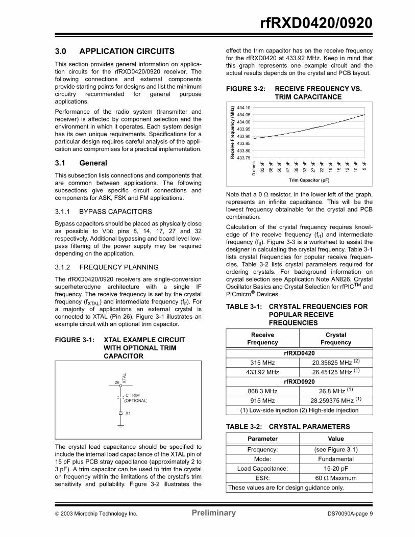
connected to XTAL (Pin 26). Figure 3-1 illustrates an
example circuit with an optional trim capacitor.
FIGURE 3-1: XTAL EXAMPLE CIRCUIT
WITH OPTIONAL TRIM
CAPACITOR
The crystal load capacitance should be specified to
include the internal load capacitance of the XTAL pin of
15 pF plus PCB stray capacitance (approximately 2 to
3 pF). A trim capacitor can be used to trim the crystal
on frequency within the limitations of the crystal’s trim
sensitivity and pullability. Figure 3-2 illustrates the
effect the trim capacitor has on the receive frequency
for the rfRXD0420 at 433.92 MHz. Keep in mind that
this graph represents one example circuit and the
actual results depends on the crystal and PCB layout.
FIGURE 3-2: RECEIVE FREQUENCY VS.
TRIM CAPACITANCE
Note that a 0 Ω resistor, in the lower left of the graph,
represents an infinite capacitance. This will be the
lowest frequency obtainable for the crystal and PCB
combination.
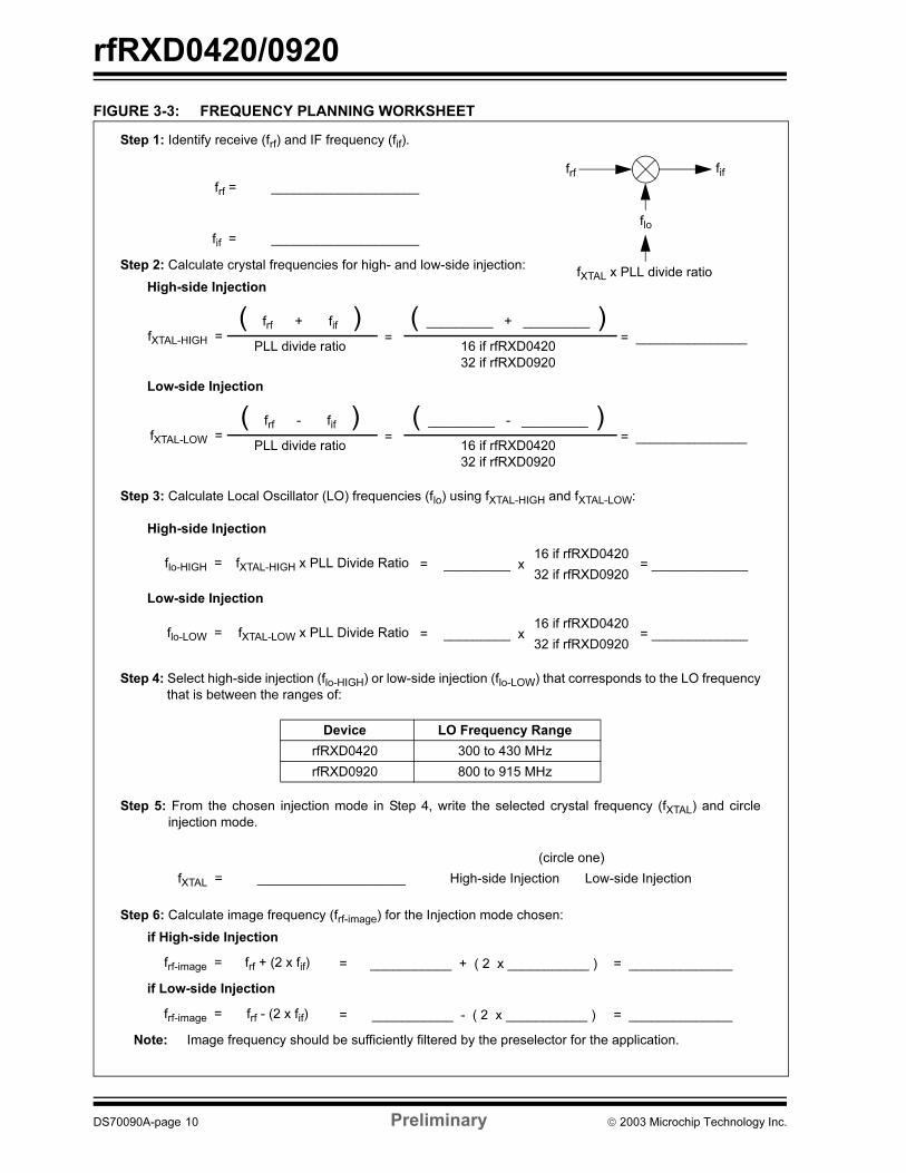
Calculation of the crystal frequency requires knowl-
edge of the receive frequency (frf) and intermediate
frequency (fif). Figure 3-3 is a worksheet to assist the
designer in calculating the crystal frequency. Table 3-1
lists crystal frequencies for popular receive frequen-
cies. Table 3-2 lists crystal parameters required for
ordering crystals. For background information on
crystal selection see Application Note AN826, Crystal
Oscillator Basics and Crystal Selection for rfPICTM and
PICmicro® Devices.
XT
AL
26
C TRIM
(OPTIONAL)
X1
TABLE 3-1: CRYSTAL FREQUENCIES FOR
POPULAR RECEIVE
FREQUENCIES
Receive
Frequency
Crystal
Frequency
rfRXD0420
315 MHz 20.35625 MHz (2)
433.92 MHz 26.45125 MHz (1)
rfRXD0920
868.3 MHz 26.8 MHz (1)
915 MHz 28.259375 MHz (1)
(1) Low-side injection (2) High-side injection
TABLE 3-2: CRYSTAL PARAMETERS
Parameter Value
Frequency: (see Figure 3-1)
Mode: Fundamental
Load Capacitance: 15-20 pF
ESR: 60 Ω Maximum
These values are for design guidance only.
433.75
433.80
433.85
433.90
433.95
434.00
434.05
434.10
0 o
hm
s
82 p
F
68 p
F
56 p
F
47 p
F
39 p
F
33 p
F
27 p
F
22 p
F
18 p
F
15 p
F
12 p
F
10 p
F
5 p
F
Trim Capacitor (pF)
Receiv
e F
req
uen
cy (
MH
z)
2003 Microchip Technology Inc. Preliminary DS70090A-page 9
rfRXD0420/0920
FIGURE 3-3: FREQUENCY PLANNING WORKSHEET
Step 1: Identify receive (frf) and IF frequency (fif).
Step 2: Calculate crystal frequencies for high- and low-side injection:
High-side Injection
Low-side Injection
Step 3: Calculate Local Oscillator (LO) frequencies (flo) using fXTAL-HIGH and fXTAL-LOW:
High-side Injection
Low-side Injection
Step 4: Select high-side injection (flo-HIGH) or low-side injection (flo-LOW) that corresponds to the LO frequency
that is between the ranges of:
Step 5: From the chosen injection mode in Step 4, write the selected crystal frequency (fXTAL) and circle
injection mode.
Step 6: Calculate image frequency (frf-image) for the Injection mode chosen:
if High-side Injection
if Low-side Injection
Note: Image frequency should be sufficiently filtered by the preselector for the application.
frf = ____________________
fif = ____________________
fXTAL-HIGH =( frf + fif )
=
( _________ + _________ ) = _______________
PLL divide ratio 16 if rfRXD0420
32 if rfRXD0920
fXTAL-LOW =( frf - fif )
=
( _________ - _________ ) = _______________
PLL divide ratio 16 if rfRXD0420
32 if rfRXD0920
flo-HIGH = fXTAL-HIGH x PLL Divide Ratio = _________ x16 if rfRXD0420
= _____________32 if rfRXD0920
flo-LOW = fXTAL-LOW x PLL Divide Ratio = _________ x16 if rfRXD0420
= _____________32 if rfRXD0920
Device LO Frequency Range
rfRXD0420 300 to 430 MHz
rfRXD0920 800 to 915 MHz
(circle one)
fXTAL = ____________________ High-side Injection Low-side Injection
frf-image = frf + (2 x fif) = ___________ + ( 2 x ___________ ) = ______________
frf-image = frf - (2 x fif) = ___________ - ( 2 x ___________ ) = ______________
frf fif
flo
fXTAL x PLL divide ratio
DS70090A-page 10 Preliminary 2003 Microchip Technology Inc.

rfRXD0420/0920
3.1.3 PLL LOOP FILTER
An external PLL loop filter is connected to pin LF
(Pin 29). The loop filter controls the dynamic behavior
of the PLL, primarily lock time and spur levels. Gener-
ally, the PLL lock time is a small fraction of the overall
receiver start-up time (see Electrical Characteristics
Section). The crystal oscillator is the largest contributor
to start-up time. Thus, for the majority of applications,
design loop filter values for a wide loop bandwidth to
suppress noise. Figure 3-4 illustrates an example filter
circuit for a wide frequency range suitable for a majority
of applications.
FIGURE 3-4: PLL LOOP FILTER EXAMPLE
CIRCUIT
3.1.4 PRESELECTOR
Receiver performance is heavily influenced by the
preselector (also known as the front-end filter). The
purpose of the preselector is to filter unwanted signals
and noise from entering the receiver.
The most important unwanted signal is the image
frequency (frf-image). Pay particular attention to the
image frequency calculated in Figure 3-3 as this will be
the frequency that needs to be filtered out by the
preselector.
The preselector can be designed using a simple LC
filter or a Surface Acoustic Wave (SAW) filter. A simple
LC filter provides a low cost solution but will have the
least effect filtering the image frequency. A SAW filter
can effectively filter the image frequency with a
minimum of 40 dB attenuation.
The SAW filter has the added advantage of filtering
wide-band noise and improving the signal-to-noise
ratio (SNR) of the receiver.
SAW filters require impedance matching. Refer to the
manufacturers' data sheet and application notes for
SAW filter pinouts, specified impedances and recom-
mended matching circuits. Figure 3-5 shows a SAW
filter example circuit.
A secondary purpose of the preselector is to provide
impedance matching between the antenna and LNAIN
(Pin 31).
3.1.5 ANTENNA
Receiver performance and device packaging influence
antenna selection. There are many third-party anten-
nas to choose from. Third-party antennas typically
have an impedance of 50 Ω. The preselector compo-
nents should be chosen to match the impedance of the
antenna to the LNAIN (Pin 31) impedance of
26 Ω || 2 pF.
The designer can chose to use a simple wire antenna.
The length of the wire should be one-quarter the wave-
length (λ) of the receive frequency. For example, the
wavelength of 433.92 MHz is:
λ = c / frf where c = 3 x 10⁸ m/s
λ = 3 x 10⁸ m/s / 433.92 x 10⁶ Hz
λ = 0.69 m
therefore
0.25λ = 17.3 cm or 6.8 inches
Finally, the wire antenna should be impedance
matched to the preselector. The typical impedance of a
one-quarter wavelength wire antenna is 36 Ω.
3.1.6 LNA GAIN
For a majority of applications, LNAGAIN can be tied to
Vss (ground) enabling High Gain mode. If the applica-
tion requires short range communications, LNAGAIN
can be tied to VDD (pulled up) enabling Low Gain mode.
More Information on LNAGAIN operation can be found
in the Circuit Description section.
FIGURE 3-5: SAW FILTER EXAMPLE CIRCUIT
LF
29
10 kΩ
1000 pFOPTIONALC1
R1
C2
LNAINAntenna
C1 C2
L1 L2
Input
Input Gnd
Output
Output Gnd
3 4 7 8
Case Gnd
SAW FilterF1
2
1
5
6
Note: Refer to SAW filter manufacturer’s data sheet for pin outs
and values for impedance matching components.
2003 Microchip Technology Inc. Preliminary DS70090A-page 11

rfRXD0420/0920
3.1.7 LNA TUNED CIRCUIT
The LNAOUT (Pin 3) has an open-collector output. It is
pulled up to VDD via a tuned circuit. It is also connected
to 1IFIN (Pin 4) via a series decoupling capacitor. The
1IFIN input impedance is approximately 33 Ω || 1.5 pF.
Important: To ensure LNA stability the VSS pin (Pin 1)
must be connected to a low impedance ground.
As shown in Figure 3-6, components C1 and L1 make
up the tuned circuit and provide collector current via
pull-up. Together with decoupling capacitor C2, they
provided impedance matching between the LNA and
MIXER1. To a lesser extent, C1, L1, and C2 provide
band-pass filtering at the receive frequency (frf).
Component values depend on the selected receive
frequency. The challenge is to design the circuit with
the fewest components setting Q as high as possible
as limited by component tolerances. For a majority of
applications it is best to design a wide bandwidth tuned
circuit to account for manufacturing and component
tolerances. The best approach is to design the tuned
circuit using a filter simulation program. Table 3-3 lists
example component values for popular receive
frequencies.
FIGURE 3-6: LNA OUTPUT TO MIXER1
EXAMPLE CIRCUIT.
3.1.8 MIXER1 BIAS
The 1IF+ (Pin 6) and 1IF- (Pin 7) are bias connections
to the MIXER1 balanced collectors. Both pins are
open-collector outputs and are individually pulled up to
VDD by a load resistor. Figure 3-7 shows a MIXER1
bias example circuit.
FIGURE 3-7: MIXER1 BIAS EXAMPLE
CIRCUIT
3.1.9 INTERMEDIATE FREQUENCY (IF)
FILTER
The IF filter defines the overall adjacent signal selectiv-
ity of the receiver. For a majority of applications, low-
cost 10.7 MHz ceramic IF filters are used. These are
available in a variety of bandwidths and packages.
IF filter bandwidth selection is a function of:
• modulation (ASK, FSK or FM)
• signal bandwidth
• frequency and temperature tolerances of the
transmitter and receiver components
The typical input and output impedance of ceramic
filters is 330 Ω. 1IFOUT (Pin 9) has an approximately
330 Ω single-ended output impedance and provides a
direct match to the ceramic IF filter. The internal resis-
tance of the 2IFIN (Pin 11) is approximately 2.2 kΩ. In
order to terminate ceramic IF filters a 390 Ω resistor
can be paralleled to the 2IFIN and FBC2 (Pin 13).
Figure 3-8 shows an example circuit schematic using a
10.7 MHz ceramic IF filter.
3.1.10 IF LIMITING AMPLIFIER EXTERNAL
FEEDBACK CAPACITORS
FBC1 (Pin 12) and FBC2 (Pin 13) are connected to
external feedback capacitors. Figure 3-8 shows
component values and connections for these
capacitors.
TABLE 3-3: LNA TUNED CIRCUIT EXAMPLE
COMPONENT VALUES
frf C1 L1 C2
315 MHz 7.0 pF 22 nH 6.0 pF
433.92 MHz 3.0 pF 15 nH 6.0 pF
868.3 MHz 2.0 pF 7.6 nH 3.0 pF
915 MHz 2.0 pF 6.8 nH 3.0 pF
These values are for design guidance only.
LN
A 1IF
3 4
OU
T
IN
VDD
C Bypass
C1
C2
L1
1IF
+
1IF
-76
VDDVDD
R1470 Ω
R2
470 Ω
DS70090A-page 12 Preliminary 2003 Microchip Technology Inc.

rfRXD0420/0920
FIGURE 3-8: IF FILTER, LIMITING AMPLIFIER AND DEMODULATOR BLOCK DIAGRAM
11
12
13
21
2IF
FB
C1
FB
C2
RS
SI
16
15
2IF
DEM
OU
T+
OU
T-
24
23
DE
MO
D
IN
OUT
IN
DE
M
DE
M
IF L
imitin
g A
mplif
ier
MIX
ER
2
with R
SS
I
+ + --
+ -O
UT
9
1IF
1000 p
F
1000 p
F
33000 p
F
Cera
mic
Filt
er
10.7
MH
z
R1
50 Ω
R2
36 k
Ω
2.2
kΩ
2.2
kΩ
390 Ω
Exte
rnal F
eedback
Capacitors
IF P
ream
p
2003 Microchip Technology Inc. Preliminary DS70090A-page 13

rfRXD0420/0920
FIGURE 3-9: ASK APPLICATION CIRCUIT
LN
ALN
A
LNA
1IF
31
34
1IF+
1IF-
76
911
12
13
21
1IF
2IF
FBC1
FBC2
RS
SI
20
19
18
OP
A+
OP
A-
OPA
XTAL
LF
29
26
Bia
sENRX
28
LNA
2
OP
A
16
15
2IF
DEM ++--
+-
OUT+
OUT-
24
23D
EM
OD
IN
OUT
IN
OUT
IN
GAIN
OUT
IN
VSS
1
VSS
5
VDD
8
VSS
10
VDD
14
VDD
17
VD
D
32 VS
S
30
27
VDD
25
VSS
DEM
DEM
MIX
ER
1IF
Pre
am
p
IF L
imitin
g A
mplif
ier
MIXER2
22
VSS
with R
SS
I
+V
+V
+V
+V
+V
+V
+V
+V
AN
T
RxD
AT
A
C1
18
00
pF
C2
47
00
0 p
F
C3
330 p
F
C4
33
0p
FC
73
30
pF
C9
OP
TIO
NA
L
C10
OP
TIO
NA
LC
11
1000pF
C12
1000 p
F
C131000 pF
C14
330 p
F
C16
330 p
FC
18
330 p
F
C8
33000 p
F
C15
C17
F2
10.7
MH
zL3
R1
10
0 k
Ω
R3
10 k
Ω
R2
390 Ω
R4
470 Ω
R5
470 Ω
X1
LO
OP
FIL
TE
RC
AP
AC
ITO
R
NC
NC
TO
AN
TE
NN
A
MA
TC
HIN
G
NE
TW
OR
K
CR
YS
TA
L T
RIM
CA
PA
CIT
OR
Cry
sta
l
Oscill
ato
r
Phase D
ete
cto
rand
Charg
e P
um
p
Voltage
Contr
olle
dO
scill
ato
r
Fix
ed D
ivid
e b
yF
requency
Synth
esiz
er
16:
rfR
XD
0420
32:
rfR
XD
0920
NC
NC
DS70090A-page 14 Preliminary 2003 Microchip Technology Inc.

rfRXD0420/0920
3.2 Amplitude Shift Keying (ASK)
Figure 3-9 illustrates an example ASK applications cir-
cuit.
The IF Limiting Amplifier with RSSI is used as an ASK
detector. The RSSI signal is post detector filtered and
then compared to a reference voltage to determine if
the incoming RF signal is a logical one or zero. The
reference voltage can be configured as a dynamic
voltage level determined by the incoming RF signal
strength or by a predetermined fixed level.
3.2.1 RSSI POST DETECTOR FILTERING
The RSSI signal is low-passed filtered to remove high
frequency and pulse noise to aid the decision making
process of the comparator and increase the sensitivity
of the receiver. The RSSI signal low-pass filter is a RC
filter created by the RSSI output impedance of 36 kΩ
and capacitor C1. Setting the time constant (RC = τ) of
the RC filter depends on the signal period and when the
signal decision will be made.
3.2.1.1 Signal Period
Optimum sensitivity of the receiver with reasonable
pulse distortion occurs when the RC filter time constant
is between 1 and 2 times the signal period. If the time
constant of the RC filter is set too short, there is little
noise filtering benefit. However, if the time constant of
the RC filter is set too long, the data pulses will become
elongated causing inter-symbol interference.
3.2.1.2 Signal Decision
If the bit decision occurs in the center of the signal
period (such as KEELOQ decoders), then one or two
times the RC filter time constant should be set at less
than or equal to half the signal period. Figure 3-10 illus-
trates this method. The top trace represents the
received on-off keying (OOK) signal. The bottom trace
shows the RSSI signal after the RC low-pass filter.
FIGURE 3-10: CENTER SIGNAL PERIOD
DECISION RSSI LOW-PASS
FILTERED
If the bit decision occurs near the end of the signal
period, then the time constant should be set at less
than or equal to the signal period. Figure 3-11
illustrates this method.
Once the signal decision time and time period of the
signal period are known, then capacitor C1 can be
selected. Once C1 is selected, the designer should
observe the RSSI signal with an oscilloscope and
perform operational and/or bit error rate testing to
confirm receiver performance.
FIGURE 3-11: NEAR END OF THE SIGNAL
PERIOD DECISION RSSI LOW-
PASS FILTERED
3.2.2 COMPARATOR
The internal operational amplifier is configured as a
comparator. The RSSI signal is applied to OPA+ (Pin
20) and compared with a reference voltage on OPA-
(Pin 19) to determine the logic level of the received
signal. The reference voltage can be dynamic or static.
The choice of dynamic versus static reference voltage
depends in part on the ratio of logical ones versus
zeros of the data (this can also be thought of as the AC
content of the data). Provided the ratio has an even
number of logical ones versus zeros, a dynamic refer-
ence voltage can be generated with a simple low-pass
filter. The advantage of the dynamic reference voltage
is the increased receiver sensitivity compared to a fixed
reference voltage. However, the comparator will output
random data. The decoder (for example, a pro-
grammed PICmicro MCU or KEELOQ decoder) must
distinguish between random noise and valid data.
The choice of a static reference voltage depends in part
on the DC content of the data. That is, the data has an
uneven number of logical ones versus zeros. The
disadvantage of the static reference voltage is
decreased receiver sensitivity compared to a dynamic
reference voltage. In this case, the comparator will
output data without random noise.
Signal Period
1τ to 2τ
Signal Decision
OOK Signal
RSSI Signal
Signal Period
1τ to 2τ
Signal Decision
OOK Signal
RSSI Signal
2003 Microchip Technology Inc. Preliminary DS70090A-page 15
rfRXD0420/0920
3.2.2.1 DYNAMIC REFERENCE VOLTAGE
A dynamic reference voltage can be derived by averag-
ing the received signal with a low-pass filter. The exam-
ple ASK application circuit shown in Figure 3-9, the
low-pass filter is formed by R1 and C2. The output of
the low-pass filter is then fed to OPA-.
The setting of the R1-C2 time constant depends on the
ratio of logical ones versus zeros and a trade off in
stability versus receiver reaction time. If the received
signal has an even number of logical ones versus
zeros, the time constant can be set relatively short.
Thus the reference voltage can react quickly to
changes in the received signal amplitude and differ-
ences in transmitters. However, it may not be as stable
and can fluctuate with the ratio of logical ones and
zeros. If the time constant is set long, the reference
voltage will be more stable. However, the receiver
cannot react as quickly upon the reception of a
received signal.
Selection of component values for R1 and C2 is an
iterative process. First start with a time constant
between 10 to 100 times the signal rate. Second, view
the reference voltage against the RSSI signal to
determine if the values are suitable. Figure 3-12 is an
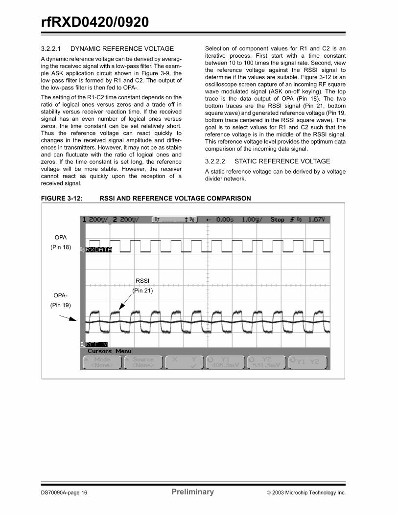
oscilloscope screen capture of an incoming RF square
wave modulated signal (ASK on-off keying). The top
trace is the data output of OPA (Pin 18). The two
bottom traces are the RSSI signal (Pin 21, bottom
square wave) and generated reference voltage (Pin 19,
bottom trace centered in the RSSI square wave). The
goal is to select values for R1 and C2 such that the
reference voltage is in the middle of the RSSI signal.
This reference voltage level provides the optimum data
comparison of the incoming data signal.
3.2.2.2 STATIC REFERENCE VOLTAGE
A static reference voltage can be derived by a voltage
divider network.
FIGURE 3-12: RSSI AND REFERENCE VOLTAGE COMPARISON
OPA
(Pin 18)
OPA-
(Pin 19)
RSSI
(Pin 21)
DS70090A-page 16 Preliminary 2003 Microchip Technology Inc.
rfRXD0420/0920
FIGURE 3-13: FSK APPLICATION CIRCUIT
LN
ALN
A
LNA
1IF
31
34
1IF+
1IF-
76
911
12
13
21
1IF
2IF
FBC1
FBC2
RS
SI
20
19
18
OP
A+
OP
A-
OPA
XTAL
LF
29
26
Bia
s ENRX
28
LNA
2
OP
A
16
15
2IF
DEM +-
+-
OUT+
OUT-
24
23DE
MO
D
IN
OUT
IN
OUT
IN
GAIN
OUT
IN
VSS
1
VSS
5
VDD
8
VSS
10
VDD
14
VDD
17
VD
D
32
VS
S
30
27
VDD
25
VSS
DEM
DEM
MIX
ER
1
IF P
ream
p
IF L
imitin
g A
mplif
ier
MIXER2
22
VSS
with R
SS
I
+V
+V
+V
+V
+V
+V
+V
+V
RS
SI
AN
T
RxD
AT
A
C1
10
-47
pF
C2
10
-47
pF
C3
330 p
F
C4
33
0 p
F
C7
33
0 p
F
C9
OP
TIO
NA
L
C10
OP
TIO
NA
LC
11
1000 p
F
C12
1000 p
F
C131000 pF
C14
330 p
F
C16
330 p
FC
18
330 p
F
C3
033
0 p
F
C3
2
68
0 p
F
C8
33000 p
F
C15
C17
C31
10
-12
pF
C3
3
1.0
pF
F2
10.7
MH
z
F3
L3
R3
10 k
Ω
R2
390 Ω
R4
470 Ω
R5
470 Ω
X1
TO
AN
TE
NN
AM
AT
CH
ING
NE
TW
OR
K
NO
TE
:D
em
od
ula
tor
ou
tpu
tlo
w-p
ass c
ap
acito
rsd
ep
en
de
nt
on
sig
na
l ra
te
Cry
sta
lO
scill
ato
r
Phase D
ete
cto
rand
Charg
e P
um
p
Voltage
Contr
olle
dO
scill
ato
r
Fix
ed D
ivid
e b
yF
requency
Synth
esiz
er
16:
rfR
XD
0420
32:
rfR
XD
0920
LO
OP
FIL
TE
RC
AP
AC
ITO
RC
RY
ST
AL T
RIM
CA
PA
CIT
OR
2003 Microchip Technology Inc. Preliminary DS70090A-page 17

rfRXD0420/0920
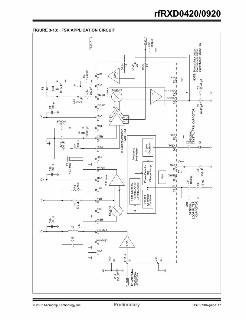
3.3 Frequency Shift Keying (FSK)
Figure 3-13 illustrates an example FSK application
circuit.
3.3.1 IF FILTER CONSIDERATIONS
As mentioned in the Section 3.1 above, IF filter band-
width selection is a function of:
• modulation (ASK, FSK or FM)
• signal bandwidth
• frequency and temperature tolerances of the
transmitter and receiver components
The occupied bandwidth of binary FSK signals is 2
times the peak frequency deviation plus 2 times the
signal bandwidth. For example, if the data rate is 2400
bits per second Manchester encoded, the signal band-
width is 4800 baud or 1200 Hz, and if the peak
frequency deviation is 24 kHz, the minimum bandwidth
of the IF filter is:
Add to this value the frequency and temperature
tolerances of the transmitter and receiver components.
FSK signals are more sensitive to group delay varia-
tions of the IF filter. Therefore, a filter with a low group
delay variation should be used. As an alternative, a
filter with wider than required bandwidth can be used
because the group delay variation in the center of the
bandpass will be relatively constant.
3.3.2 FSK DETECTOR
The demodulator (DEMOD) section consists of a phase
detector (MIXER2) and amplifier creating a quadrature
detector (also known as a phase coincidence detector)
to demodulate the IF signal in FSK and FM modulation
applications. The in-phase signal comes directly from
the output of the IF limiting amplifier to MIXER2. The
quadrature signal is created by an external tuned circuit
from the output of the IF limiting amplifier (2IFOUT, Pin
15) AC-coupled to the MIXER2 DEMIN (Pin 16) input.
3.3.2.1 LC Discriminator
The external tuned circuit can be constructed from
simple inductor-capacitor (LC) components. This type
circuit produces and excellent output. However, one of
the elements (L or C) must be tunable. Figure 3-14
illustrates an example LC discriminator circuit using a
tunable capacitor. A similar circuit with a tunable induc-
tor is also possible. Resistor R1 = 4.7 kΩ reduces the
Q of the circuit so that frequency deviations of up to 75
kHz can be demodulated.
FIGURE 3-14: LC DISCRIMINATOR
EXAMPLE CIRCUIT
3.3.2.2 Ceramic Discriminator
A no-tune solution can be constructed with a ceramic
discriminator. Figure 3-15 illustrates an example
ceramic discriminator circuit.
The ceramic discriminator acts as a parallel tuned
circuit at the IF frequency (for example, 10.7 MHz). The
parallel capacitor C3 tunes the ceramic resonator. The
high Q of this circuit enables higher output of the detec-
tor for small frequency deviations. However, smaller
frequency deviations require better frequency
tolerances at the transmitter and receiver.
In order to detect wider deviation or off-frequency
signals, the detector bandwidth has to be increased.
This can be accomplished by reducing the Q of the
tuned circuit. One method is to parallel a resistor
across the ceramic discriminator. A second is to
increase the value of the coupling capacitor C1
increasing the load on the detector. The result of
reducing the Q of the discriminator will be that the
detector output will be smaller.
FIGURE 3-15: CERAMIC DISCRIMINATOR
EXAMPLE CIRCUIT
IF BWmin = (2 x 2400) + (2 x 24000)
IF BWmin = 52800 Hz
1615
2IF
DE
MOU
T
IN
C2680 pF
C11.0 pF
0-56 pFC3
3.3 µHL1
R14.7 kΩ
1615
2IF
DE
MOU
T
IN
C2680 pF
C11.0 pF
C310-12 pF
F1
CERAMIC DISCRIMINATOR
DS70090A-page 18 Preliminary 2003 Microchip Technology Inc.

rfRXD0420/0920
3.3.3 POST DETECTOR FILTERING
Care should be taken in selecting the values of capac-
itors C1 and C2 (Figure 3-13) so that the output of the
detector is not distorted and receiver sensitivity
improved. These values are chosen depending on the
data signal rate.
Generally, if the data signal rate is fast then the filter
time constant can be set short. Conversely, if the signal
rate is slow, the filter time constant can be set long. The
designer should observe the output of the detector with
an oscilloscope and perform operational and/or bit
error rate testing to confirm receiver performance.
3.3.4 COMPARATOR
The output of the DEMOD amplifier (DEMOUT+ and
DEMOUT-, Pins 23 and 24) depends on the peak
deviation of the FSK or FM signal and the Q of the
external tuned circuit. DEMout+ and DEMout- are high
impedance outputs with only a 20 µA current capability.
The capacitance on these pins limit the maximum data
signal rate. The nominal output voltage of these pins is
1.23V.
2003 Microchip Technology Inc. Preliminary DS70090A-page 19

rfRXD0420/0920
FIGURE 3-16: FM APPLICATION CIRCUIT
LN
ALN
A
LNA
1IF
31
34
1IF+
1IF-
76
911
12
13
21
1IF
2IF
FBC1
FBC2
RS
SI
20
19
18
OP
A+
OP
A-
OPA
XTAL
LF
29
26
Bia
s
ENRX
28
LNA
2
OP
A
16
15
2IF
DEM ++--
+-
OUT+
OUT-
24
23D
EM
OD
IN
OUT
IN
OUT
IN
GAIN
OUT
IN
VSS
1
VSS
5
VDD
8
VSS
10
VDD
14
VDD
17
VD
D
32 VS
S
30
27
VDD
25
VSS
DEM
DEM
MIX
ER
1IF
Pre
am
p
IF L
imitin
g A
mplif
ier
MIXER2
22
VSS
with R
SS
I
+V
+V
+V
+V
+V
+V
+V
+V
RxA
ud
io
AN
T
RS
SI
C1
330 p
F
C3
330 p
F
C4
33
0 p
F
C4
33
0 p
F
C9
OP
TIO
NA
LC
11
1000 p
F
C12
1000 p
F
C131000 pF
C14
330 p
F
C16
330 p
F
C18
OP
TIO
NA
L
C3
033
0 p
F
C32
68
0 p
F
C34
10
0 p
F
C35
10
0 p
F
C8
33000 p
F
C15
C17
C3
1
10
-12
pF
C33
1.0
pF
F1
10.7
MH
z
F3
L3
R3
10 k
Ω
R3
0
6.8
kΩ
R31
12
kΩ
R32
33
kΩ
R3
3
33
kΩ
R2
390 Ω
R4
470 Ω
R5
470 Ω
X1
LO
OP
FIL
TE
R
CA
PA
CIT
OR
TO
AN
TE
NN
A
MA
TC
HIN
G
NE
TW
OR
K
NC
Cry
sta
l
Oscill
ato
r
Phase D
ete
cto
rand
Charg
e P
um
p
Voltage
Contr
olle
dO
scill
ato
r
Fix
ed D
ivid
e b
yF
requency
Synth
esiz
er
16: rf
RX
D0420
32: rf
RX
D0920
CR
YS
TA
L T
RIM
CA
PA
CIT
OR
DS70090A-page 20 Preliminary 2003 Microchip Technology Inc.

rfRXD0420/0920
3.4 Frequency Modulation (FM)
Figure 3-16 illustrates an example FM application
circuit.
3.4.1 FSK DETECTOR
FM demodulation is performed in the same manner as
described in the FSK section above.
3.4.2 OPERATIONAL AMPLIFIER
The internal operational amplifier is configured as an
active low-pass filter.
FM audio is typically de-emphasized. It is recom-
mended that de-emphasis circuitry be connected at the
output of the operational amplifier rather than the
output of the detector.
2003 Microchip Technology Inc. Preliminary DS70090A-page 21
rfRXD0420/0920
4.0 ELECTRICAL CHARACTERISTICS
Absolute Maximum Ratings
Supply voltage...................................................................................................................................................0 to +7.0V
Input voltage...........................................................................................................................................-0.3 to VCC+0.3V
Input RF level .........................................................................................................................................................10dBm
Storage temperature .................................................................................................................................... -40 to +125C
† NOTICE: Stresses above those listed under “Absolute Maximum Ratings” may cause permanent damage to the
device. This is a stress rating only and functional operation of the device at those or any other conditions above those
indicated in the operation listings of this specification is not implied. Exposure to maximum rating conditions for
extended periods may affect device reliability.
DS70090A-page 22 Preliminary 2003 Microchip Technology Inc.

rfRXD0420/0920
4.1 DC Characteristics: rfRXD0420
(Industrial)
* These parameters are characterized but not tested.
† Data in “Typ” column is at 3V, 23°C unless otherwise stated. These parameters are for design guidance only and
are not tested.
4.2 AC Characteristics: rfRXD0420
(Industrial)
* These parameters are characterized but not tested.
† Data in “Typ” column is at 3V, 23°C, frf = 433.6 MHz, IF = 10.7 MHz unless otherwise stated. These parameters
are for design guidance only and are not tested.
Note 1: Dependant on ASK detector time constant.
2: IF bandwidth = 40 kHz, ∆f = +/- 15 kHz, BER <= 3 x 10⁻³
3: IF bandwidth = 150 kHz, ∆f = +/- 50 kHz, BER <= 3 x 10⁻³
4: IF bandwidth = 40 kHz, BER <= 3 x 10⁻³
5: IF bandwidth = 150 kHz, BER <= 3 x 10⁻³
DC CHARACTERISTICSStandard Operating Conditions (unless otherwise stated)
Operating Temperature -40°C ≤ TA ≤ +85°C
Param
No.Sym Characteristic Min Typ† Max Units Conditions
VCC Supply Voltage 2.5 — 5.5 V frf < 400 MHz
2.7 — 5.5 V frf > 400 MHz
ISTBY Standby Current 100 nA ENRX = 0
ICC Supply Current 5.0 6.5 8.0 mA LNAGAIN = 1
6.5 8.2 10.0 mA LNAGAIN = 0
VOPA Op Amp input voltage offset -20 — 20 mV
IOPA Op Amp input current offset -50 — 50 nA
IBIAS Op Amp input bias current -100 100 nA
VRSSI RSSI voltage 0.5 1.0 1.5 V LNAGAIN = 1
1.25 1.9 2.45 V LNAGAIN = 0
AC CHARACTERISTICSStandard Operating Conditions (unless otherwise stated)
Operating Temperature -40°C ≤ TA ≤ +85°C
Param
No.Sym Characteristic Min Typ† Max Units Conditions
TFSK Start-up time - FSK/FM 0.9 ms ENRX = 0 to 1
TASK Start-up time - ASK R1xC1
+TFSK
ms Note 1
Sensitivity - Narrowband FSK -111 dBm Note 2
Sensitivity - Wideband FSK -104 dBm Note 3
Sensitivity - Narrowband ASK -109 dBm Note 4
Sensitivity - Wideband ASK -106 dBm Note 5
Input RF level maximum FSK/
FM
0 dBm LNAGAIN = 1
Input RF level maximum ASK -10 dBm LNAGAIN = 1
2003 Microchip Technology Inc. Preliminary DS70090A-page 23
rfRXD0420/0920
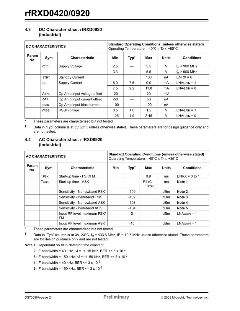
4.3 DC Characteristics: rfRXD0920
(Industrial)
* These parameters are characterized but not tested.
† Data in “Typ” column is at 3V, 23°C unless otherwise stated. These parameters are for design guidance only and
are not tested.
4.4 AC Characteristics: rfRXD0920
(Industrial)
* These parameters are characterized but not tested.
† Data in “Typ” column is at 3V, 23°C, frf = 433.6 MHz, IF = 10.7 MHz unless otherwise stated. These parameters
are for design guidance only and are not tested.
Note 1: Dependant on ASK detector time constant.
2: IF bandwidth = 40 kHz, ∆f = +/- 15 kHz, BER <= 3 x 10⁻³
3: IF bandwidth = 150 kHz, ∆f = +/- 50 kHz, BER <= 3 x 10⁻³
4: IF bandwidth = 40 kHz, BER <= 3 x 10⁻³
5: IF bandwidth = 150 kHz, BER <= 3 x 10⁻³
DC CHARACTERISTICSStandard Operating Conditions (unless otherwise stated)
Operating Temperature -40°C ≤ TA ≤ +85°C
Param
No.Sym Characteristic Min Typ† Max Units Conditions
VCC Supply Voltage 2.5 — 5.5 V frf < 900 MHz
3.3 — 5.5 V frf > 900 MHz
ISTBY Standby Current 100 nA ENRX = 0
ICC Supply Current 6.0 7.5 9.0 mA LNAGAIN = 1
7.5 9.2 11.0 mA LNAGAIN = 0
VOPA Op Amp input voltage offset -20 — 20 mV
IOPA Op Amp input current offset -50 — 50 nA
IBIAS Op Amp input bias current -100 100 nA
VRSSI RSSI voltage 0.5 1.0 1.5 V LNAGAIN = 1
1.25 1.9 2.45 V LNAGAIN = 0
AC CHARACTERISTICSStandard Operating Conditions (unless otherwise stated)
Operating Temperature -40°C ≤ TA ≤ +85°C
Param
No.Sym Characteristic Min Typ† Max Units Conditions
TFSK Start-up time - FSK/FM 0.9 ms ENRX = 0 to 1
TASK Start-up time - ASK R1xC1
+ TFSK
ms Note 1
Sensitivity - Narrowband FSK -109 dBm Note 2
Sensitivity - Wideband FSK -102 dBm Note 3
Sensitivity - Narrowband ASK -108 dBm Note 4
Sensitivity - Wideband ASK -104 dBm Note 5
Input RF level maximum FSK/
FM
0 dBm LNAGAIN = 1
Input RF level maximum ASK -10 dBm LNAGAIN = 1
DS70090A-page 24 Preliminary 2003 Microchip Technology Inc.

rfRXD0420/0920
5.0 PACKAGING INFORMATION
5.1 Package Marking Information
Legend: XX...X Customer specific information*
Y Year code (last digit of calendar year)
YY Year code (last 2 digits of calendar year)
WW Week code (week of January 1 is week ‘01’)
NNN Alphanumeric traceability code
Note: In the event the full Microchip part number cannot be marked on one line, it will
be carried over to the next line thus limiting the number of available characters
for customer specific information.
* Standard PICmicro device marking consists of Microchip part number, year code, week code, and
traceability code. For PICmicro device marking beyond this, certain price adders apply. Please check
with your Microchip Sales Office. For QTP devices, any special marking adders are included in QTP
price.
32-Lead LQFP
XXXXXXXXXXXX
XXXXXXXXXXXX
XXXXXXXXXXXX
YYWWNNN
Example
rfRXD0420
02123ABC
2003 Microchip Technology Inc. Preliminary DS70090A-page 25

rfRXD0420/0920
5.2 Package Details
The following section gives the technical details of the package.
32-Lead Plastic Low Profile Quad Flat Package (LQ) 7 x 7 x 1.4 mm Body
Not available at this time.
DS70090A-page 26 Preliminary 2003 Microchip Technology Inc.
rfRXD0420/0920
ON-LINE SUPPORT
Microchip provides on-line support on the Microchip
World Wide Web site.
The web site is used by Microchip as a means to make
files and information easily available to customers. To
view the site, the user must have access to the Internet
and a web browser, such as Netscape® or Microsoft®
Internet Explorer. Files are also available for FTP
download from our FTP site.
Connecting to the Microchip Internet Web Site
The Microchip web site is available at the following
URL:
www.microchip.com
The file transfer site is available by using an FTP
service to connect to:
ftp://ftp.microchip.com
The web site and file transfer site provide a variety of
services. Users may download files for the latest
Development Tools, Data Sheets, Application Notes,
User's Guides, Articles and Sample Programs. A vari-
ety of Microchip specific business information is also
available, including listings of Microchip sales offices,
distributors and factory representatives. Other data
available for consideration is:
• Latest Microchip Press Releases
• Technical Support Section with Frequently Asked
Questions
• Design Tips
• Device Errata
• Job Postings
• Microchip Consultant Program Member Listing
• Links to other useful web sites related to
Microchip Products
• Conferences for products, Development Systems,
technical information and more
• Listing of seminars and events
2003 Microchip Technology Inc. Prelimin
SYSTEMS INFORMATION AND UPGRADE HOT LINE
The Systems Information and Upgrade Line provides
system users a listing of the latest versions of all of
Microchip's development systems software products.
Plus, this line provides information on how customers
can receive the most current upgrade kits.The Hot Line
Numbers are:
1-800-755-2345 for U.S. and most of Canada, and
1-480-792-7302 for the rest of the world.
092002
ary DS70090A-page 27

rfRXD0420/0920
READER RESPONSE
It is our intention to provide you with the best documentation possible to ensure successful use of your Microchip prod-
uct. If you wish to provide your comments on organization, clarity, subject matter, and ways in which our documentation
can better serve you, please FAX your comments to the Technical Publications Manager at (480) 792-4150.
Please list the following information, and use this outline to provide us with your comments about this document.
1. What are the best features of this document?
2. How does this document meet your hardware and software development needs?
3. Do you find the organization of this document easy to follow? If not, why?
4. What additions to the document do you think would enhance the structure and subject?
5. What deletions from the document could be made without affecting the overall usefulness?
6. Is there any incorrect or misleading information (what and where)?
7. How would you improve this document?
To: Technical Publications Manager
RE: Reader Response
Total Pages Sent ________
From: Name
Company
Address
City / State / ZIP / Country
Telephone: (_______) _________ - _________
Application (optional):
Would you like a reply? Y N
Device: Literature Number:
Questions:
FAX: (______) _________ - _________
DS70090ArfRXD0420/0920
DS70090A-page 28 Preliminary 2003 Microchip Technology Inc.

rfRXD0420/0920
PRODUCT IDENTIFICATION SYSTEM
To order or obtain information, e.g., on pricing or delivery, refer to the factory or the listed sales office.
Sales and Support
Data SheetsProducts supported by a preliminary Data Sheet may have an errata sheet describing minor operational differences and recom-mended workarounds. To determine if an errata sheet exists for a particular device, please contact one of the following:
1. Your local Microchip sales office2. The Microchip Corporate Literature Center U.S. FAX: (480) 792-72773. The Microchip Worldwide Site (www.microchip.com)
Please specify which device, revision of silicon and Data Sheet (include Literature #) you are using.
New Customer Notification SystemRegister on our web site (www.microchip.com/cn) to receive the most current information on our products.
PART NO. X /XX XXX
PatternPackageTemperatureRange
Device
Device rfRXD0420-I/LQ UHF ASK/FSK/FM ReceiverrfRXD0920-I/LQ UHF ASK/FSK/FM ReceiverrfRXD0420T-I/LQ UHF ASK/FSK/FM Receiver(Tape & Reel)rfRXD0920T-I/LQ UHF ASK/FSK/FM Receiver(Tape & Reel)
Temperature Range I = -40°C to +85°C
Package LQ = LQFP32
Pattern Special Requirements
Examples:
a) rfRXD0420-I/LQ = Industrial temp, LQFP
package
b) rfRXD0920-I/LQ = Industrial temp, LQFP
package
2003 Microchip Technology Inc. Preliminary DS70090A-page29

rfRXD0420/0920
NOTES:
DS70090A-page30 Preliminary 2003 Microchip Technology Inc.

Note the following details of the code protection feature on Microchip devices:
• Microchip products meet the specification contained in their particular Microchip Data Sheet.
• Microchip believes that its family of products is one of the most secure families of its kind on the market today, when used in the
intended manner and under normal conditions.
• There are dishonest and possibly illegal methods used to breach the code protection feature. All of these methods, to our
knowledge, require using the Microchip products in a manner outside the operating specifications contained in Microchip's Data
Sheets. Most likely, the person doing so is engaged in theft of intellectual property.
• Microchip is willing to work with the customer who is concerned about the integrity of their code.
• Neither Microchip nor any other semiconductor manufacturer can guarantee the security of their code. Code protection does not
mean that we are guaranteeing the product as “unbreakable.”
Code protection is constantly evolving. We at Microchip are committed to continuously improving the code protection features of our
products. Attempts to break microchip’s code protection feature may be a violation of the Digital Millennium Copyright Act. If such acts
allow unauthorized access to your software or other copyrighted work, you may have a right to sue for relief under that Act.
Information contained in this publication regarding device
applications and the like is intended through suggestion only
and may be superseded by updates. It is your responsibility to
ensure that your application meets with your specifications. No
representation or warranty is given and no liability is assumed by
Microchip Technology Incorporated with respect to the accuracy
or use of such information, or infringement of patents or other
intellectual property rights arising from such use or otherwise.
Use of Microchip’s products as critical components in life
support systems is not authorized except with express written
approval by Microchip. No licenses are conveyed, implicitly or
otherwise, under any intellectual property rights.
2003 Microchip Technology Inc. Prelimi
Trademarks
The Microchip name and logo, the Microchip logo, KEELOQ,
MPLAB, PIC, PICmicro, PICSTART, PRO MATE and
PowerSmart are registered trademarks of Microchip Technology
Incorporated in the U.S.A. and other countries.
FilterLab, microID, MXDEV, MXLAB, PICMASTER, SEEVAL
and The Embedded Control Solutions Company are registered
trademarks of Microchip Technology Incorporated in the U.S.A.
Accuron, dsPIC, dsPICDEM.net, ECONOMONITOR,
FanSense, FlexROM, fuzzyLAB, In-Circuit Serial Programming,
ICSP, ICEPIC, microPort, Migratable Memory, MPASM, MPLIB,
MPLINK, MPSIM, PICC, PICkit, PICDEM, PICDEM.net,
PowerCal, PowerInfo, PowerTool, rfPIC, Select Mode,
SmartSensor, SmartShunt, SmartTel and Total Endurance are
trademarks of Microchip Technology Incorporated in the U.S.A.
and other countries.
Serialized Quick Turn Programming (SQTP) is a service mark of
Microchip Technology Incorporated in the U.S.A.
All other trademarks mentioned herein are property of their
respective companies.
© 2003, Microchip Technology Incorporated, Printed in the
U.S.A., All Rights Reserved.
Printed on recycled paper.
nary DS70090A - page 31
Microchip received QS-9000 quality system certification for its worldwide headquarters, design and wafer fabrication facilities in Chandler and Tempe, Arizona in July 1999 and Mountain View, California in March 2002. The Company’s quality system processes and procedures are QS-9000 compliant for its PICmicro® 8-bit MCUs, KEELOQ® code hopping devices, Serial EEPROMs, microperipherals, non-volatile memory and analog products. In addition, Microchip’s quality system for the design and manufacture of development systems is ISO 9001 certified.

DS70090A-page 32 Preliminary 2003 Microchip Technology Inc.
AMERICAS
Corporate Office2355 West Chandler Blvd.Chandler, AZ 85224-6199Tel: 480-792-7200 Fax: 480-792-7277Technical Support: 480-792-7627Web Address: http://www.microchip.com
Rocky Mountain2355 West Chandler Blvd.Chandler, AZ 85224-6199Tel: 480-792-7966 Fax: 480-792-4338
Atlanta3780 Mansell Road, Suite 130Alpharetta, GA 30022Tel: 770-640-0034 Fax: 770-640-0307
Boston2 Lan Drive, Suite 120Westford, MA 01886Tel: 978-692-3848 Fax: 978-692-3821
Chicago333 Pierce Road, Suite 180Itasca, IL 60143Tel: 630-285-0071 Fax: 630-285-0075
Dallas4570 Westgrove Drive, Suite 160Addison, TX 75001Tel: 972-818-7423 Fax: 972-818-2924
DetroitTri-Atria Office Building 32255 Northwestern Highway, Suite 190Farmington Hills, MI 48334Tel: 248-538-2250 Fax: 248-538-2260
Kokomo2767 S. Albright Road Kokomo, Indiana 46902Tel: 765-864-8360 Fax: 765-864-8387
Los Angeles18201 Von Karman, Suite 1090Irvine, CA 92612Tel: 949-263-1888 Fax: 949-263-1338
San JoseMicrochip Technology Inc.2107 North First Street, Suite 590San Jose, CA 95131Tel: 408-436-7950 Fax: 408-436-7955
Toronto6285 Northam Drive, Suite 108Mississauga, Ontario L4V 1X5, CanadaTel: 905-673-0699 Fax: 905-673-6509
ASIA/PACIFIC
AustraliaMicrochip Technology Australia Pty LtdSuite 22, 41 Rawson StreetEpping 2121, NSWAustraliaTel: 61-2-9868-6733 Fax: 61-2-9868-6755
China - BeijingMicrochip Technology Consulting (Shanghai)Co., Ltd., Beijing Liaison OfficeUnit 915Bei Hai Wan Tai Bldg.No. 6 Chaoyangmen Beidajie Beijing, 100027, No. ChinaTel: 86-10-85282100 Fax: 86-10-85282104
China - ChengduMicrochip Technology Consulting (Shanghai)Co., Ltd., Chengdu Liaison OfficeRm. 2401-2402, 24th Floor, Ming Xing Financial TowerNo. 88 TIDU StreetChengdu 610016, ChinaTel: 86-28-86766200 Fax: 86-28-86766599
China - FuzhouMicrochip Technology Consulting (Shanghai)Co., Ltd., Fuzhou Liaison OfficeUnit 28F, World Trade PlazaNo. 71 Wusi RoadFuzhou 350001, ChinaTel: 86-591-7503506 Fax: 86-591-7503521
China - Hong Kong SARMicrochip Technology Hongkong Ltd.Unit 901-6, Tower 2, Metroplaza223 Hing Fong RoadKwai Fong, N.T., Hong KongTel: 852-2401-1200 Fax: 852-2401-3431
China - ShanghaiMicrochip Technology Consulting (Shanghai)Co., Ltd.Room 701, Bldg. BFar East International PlazaNo. 317 Xian Xia RoadShanghai, 200051Tel: 86-21-6275-5700 Fax: 86-21-6275-5060
China - ShenzhenMicrochip Technology Consulting (Shanghai)Co., Ltd., Shenzhen Liaison OfficeRm. 1812, 18/F, Building A, United PlazaNo. 5022 Binhe Road, Futian DistrictShenzhen 518033, ChinaTel: 86-755-82901380 Fax: 86-755-82966626
China - QingdaoRm. B503, Fullhope Plaza,No. 12 Hong Kong Central Rd.Qingdao 266071, ChinaTel: 86-532-5027355 Fax: 86-532-5027205
IndiaMicrochip Technology Inc.India Liaison OfficeDivyasree Chambers1 Floor, Wing A (A3/A4)No. 11, O’Shaugnessey RoadBangalore, 560 025, IndiaTel: 91-80-2290061 Fax: 91-80-2290062
JapanMicrochip Technology Japan K.K.Benex S-1 6F3-18-20, ShinyokohamaKohoku-Ku, Yokohama-shiKanagawa, 222-0033, JapanTel: 81-45-471- 6166 Fax: 81-45-471-6122
KoreaMicrochip Technology Korea168-1, Youngbo Bldg. 3 FloorSamsung-Dong, Kangnam-KuSeoul, Korea 135-882Tel: 82-2-554-7200 Fax: 82-2-558-5934
SingaporeMicrochip Technology Singapore Pte Ltd.200 Middle Road#07-02 Prime CentreSingapore, 188980Tel: 65-6334-8870 Fax: 65-6334-8850
TaiwanMicrochip Technology (Barbados) Inc., Taiwan Branch11F-3, No. 207Tung Hua North RoadTaipei, 105, TaiwanTel: 886-2-2717-7175 Fax: 886-2-2545-0139
EUROPEAustriaMicrochip Technology Austria GmbHDurisolstrasse 2A-4600 WelsAustriaTel: 43-7242-2244-399Fax: 43-7242-2244-393
DenmarkMicrochip Technology Nordic ApSRegus Business CentreLautrup hoj 1-3Ballerup DK-2750 DenmarkTel: 45 4420 9895 Fax: 45 4420 9910
FranceMicrochip Technology SARLParc d’Activite du Moulin de Massy43 Rue du Saule TrapuBatiment A - ler Etage91300 Massy, FranceTel: 33-1-69-53-63-20 Fax: 33-1-69-30-90-79
GermanyMicrochip Technology GmbHSteinheilstrasse 10D-85737 Ismaning, GermanyTel: 49-89-627-144 0 Fax: 49-89-627-144-44
ItalyMicrochip Technology SRLCentro Direzionale Colleoni Palazzo Taurus 1 V. Le Colleoni 120041 Agrate BrianzaMilan, Italy Tel: 39-039-65791-1 Fax: 39-039-6899883
United KingdomMicrochip Ltd.505 Eskdale RoadWinnersh TriangleWokingham Berkshire, England RG41 5TUTel: 44 118 921 5869 Fax: 44-118 921-5820
12/05/02
WORLDWIDE SALES AND SERVICE