Embed Size (px)
Citation preview
U3741BM
Rev. A2, 12-Oct-00 1 (25)
UHF ASK/FSK Receiver
DescriptionThe U3741BM is a multi-chip PLL receiver devicesupplied in an SO20 package. It has been speciallydeveloped for the demands of RF low-cost datatransmission systems with low data rates from 1 kBaud to10 kBaud (1 kBaud to 3.2 kBaud for FSK) in Manchesteror Bi-phase code. The receiver is well suited to operatewith Atmel Wireless & Microcontrollers’ PLL RF
transmitter U2741B. Its main applications are in the areasof telemetering, security technology and keyless-entrysystems. It can be used in the frequency receiving rangeof f0 = 300 MHz to 450 MHz for ASK or FSK datatransmission. All the statements made below refer to433.92-MHz and 315-MHz applications.
Features Minimal external circuitry requirements, no RF com-
ponents on the PC board except matching to thereceiver antenna
High sensitivity, especially at low data rates
Sensitivity reduction possible even while receiving
Fully integrated VCO
Low power consumption due to configurable self pol-ling with a programmable timeframe check
Supply voltage 4.5 V to 5.5 V, operating temperature range –40°C to 105°C
Single-ended RF input for easy adaptation to /4 an-tenna or printed antenna on PCB
Low-cost solution due to high integration level
ESD protection according to MIL-STD. 883 (4KV HBM) except Pin POUT (2KV HBM)
High image frequency suppression due to 1 MHz IFin conjunction with a SAW front-end filter. Up to40 dB is thereby achievable with newer SAWs.
Programmable output port for sensitivity selection orfor controlling external periphery
Communication to C possible via a single, bi-directional data line
Power management (polling) is also possible bymeans of a separate pin via the C
2 different IF bandwidth versions are available(300 kHz and 600 kHz)
System Block Diagram
Demod.
IF Amp
LNA VCO
PLL XTO
Control
U3741BM1...3
14917
C
Poweramp.
XTO VCO
PLL
U2741B
Antenna Antenna
UHF ASK/FSKRemote control transmitter
UHF ASK/FSKRemote control receiver
EncoderM44Cx9x
1 Li cell
Keys
Figure 1. System block diagram

U3741BM
Rev. A2, 12-Oct-002 (25)
Ordering Information
Extended Type Number Package RemarksU3741BM-M2FL SO20 2: IF bandwidth of 300 kHz, tube
U3741BM-M2FLG3 SO20 2: IF bandwidth of 300 kHz, taped and reeledU3741BM-M3FL SO20 3: IF bandwidth of 600 kHz, tube
U3741BM-M3FLG3 SO20 3: IF bandwidth of 600 kHz, taped and reeled
Pin Description
1
2
3
4
5
6
7
8
10
9
19
18
17
16
14
15
13
12
11
20
AVCC
AGND
14844
DGND
MIXVCC
LNAGND
LNA_IN
FSK/ASK
CDEM
POUT
MODE
XTO
LFGND
LF
ENABLE
TEST
n.c. LFVCC
DATA
DVCC
SENS
U3741BM
Figure 2. Pinning SO20
Pin Symbol Function1 SENS Sensitivity-control resistor2 FSK/ASK Selecting FSK/ASK
Low: FSK, High: ASK3 CDEM Lower cut-off frequency data filter4 AVCC Analog power supply5 AGND Analog ground6 DGND Digital ground7 MIXVCC Power supply mixer8 LNAGND High-frequency ground LNA and
mixer9 LNA_IN RF input
10 n.c. Not connected11 LFVCC Power supply VCO12 LF Loop filter13 LFGND Ground VCO14 XTO Crystal oscillator15 DVCC Digital power supply16 MODE Selecting 433.92 MHz /315 MHz
Low: 4.90625 MHz (USA)High: 6.76438 (Europe)
17 POUT Programmable output port18 TEST Test pin, during operation at GND19 ENABLE Enables the polling mode
Low: polling mode off (sleep mode)
H: polling mode on(active mode)
20 DATA Data output / configuration input

U3741BM
Rev. A2, 12-Oct-00 3 (25)
Block Diagram
15011
FSK/ASK–Demodulatorand data filter
IF Amp
IF Amp
4. Order
LPF3 MHz
LPF3 MHz
DEMOD_OUT
Limiter outRSSI
Sensitivityreduction
Standby logic
Polling circuitand
control logic
FE CLK
VCO XTO
64
f
50 k
VS
FSK/ASK
CDEM
AVCC
SENS
AGND
DGND
MIXVCC
LNAGND
LNA_IN
DATA
ENABLE
TEST
POUT
MODE
LFGND
LFVCC
XTO
LF
DVCC
LNA
Figure 3. Block diagram
RF Front EndThe RF front end of the receiver is a heterodyne configu-ration that converts the input signal into a 1-MHz IFsignal. According to figure 3, the front end consists of anLNA (low noise amplifier), LO (local oscillator), a mixerand RF amplifier.The LO generates the carrier frequency for the mixer viaa PLL synthesizer. The XTO (crystal oscillator) generatesthe reference frequency fXTO. The VCO (voltage-con-trolled oscillator) generates the drive voltage frequencyfLO for the mixer. fLO is dependent on the voltage at PinLF. fLO is divided by factor 64. The divided frequency iscompared to fXTO by the phase frequency detector. Thecurrent output of the phase frequency detector is con-nected to a passive loop filter and thereby generates thecontrol voltage VLF for the VCO. By means of that con-
figuration, VLF is controlled in a way that fLO/64 is equalto fXTO. If fLO is determined, fXTO can be calculated usingthe following formula:
fXTO = fLO/64
The XTO is a one-pin oscillator that operates at the seriesresonance of the quartz crystal. According to figure 4, thecrystal should be connected to GND via a capacitor CL.The value of that capacitor is recommended by the crystalsupplier. The value of CL should be optimized for the in-dividual board layout to achieve the exact value of fXTOand hereby of fLO. When designing the system in termsof receiving bandwidth, the accuracy of the crystal andthe XTO must be considered.

U3741BM
Rev. A2, 12-Oct-004 (25)
DVCC
XTO
LF
LFVCC
LFGND
V
C
C10R1
C9
S
L
VS
R1 = 820 C9 = 4.7 nFC10 = 1 nF
Figure 4. PLL peripherals
The passive loop filter connected to Pin LF is designed fora loop bandwidth of BLoop = 100 kHz. This value forBLoop exhibits the best possible noise performance of theLO. Figure 4 shows the appropriate loop filter compo-nents to achieve the desired loop bandwidth. If the filtercomponents are changed for any reason please note thatthe maximum capacitive load at Pin LF is limited. If thecapacitive load is exceeded, a bitcheck may no longer bepossible since fLO cannot settle in time before thebitcheck starts to evaluate the incoming data stream. Selfpolling does therefore also not work in that case.
fLO is determined by the RF input frequency fRF and theIF frequency fIF using the following formula:
fLO = fRF – fIF
To determine fLO, the construction of the IF filter must beconsidered at this point. The nominal IF frequency isfIF = 1 MHz. To achieve a good accuracy of the filter’scorner frequencies, the filter is tuned by the crystal fre-quency fXTO. This means that there is a fixed relationbetween fIF and fLO, that depends on the logic level at pinmode. This is described by the following formulas:
MODE 0 (USA) fIF fLO
314
MODE 1 (Europe) fIF fLO
432.92
The relation is designed to achieve the nominal IF fre-quency of fIF = 1 MHz for most applications. Forapplications where fRF = 315 MHz, MODE must be set to‘0’. In the case of fRF = 433.92 MHz, MODE must be setto ‘1’. For other RF frequencies, fIF is not equal to 1 MHz.fIF is then dependent on the logical level at Pin MODE andon fRF. Table 1 summarizes the different conditions.
The RF input either from an antenna or from a generatormust be transformed to the RF input Pin LNA_IN. The in-put impedance of that pin is provided in the electricalparameters. The parasitic board inductances and capaci-tances also influence the input matching. The RF receiverU3741BM exhibits its highest sensitivity at the bestsignal-to-noise ratio in the LNA. Hence, noise matchingis the best choice for designing the transformationnetwork.
A good practice when designing the network, is to startwith power matching. From that starting point, the valuesof the components can be varied to some extent to achievethe best sensitivity.
If a SAW is implemented into the input network a mirrorfrequency suppression of PRef = 40 dB can be achieved.There are SAWs available that exhibit a notch atf = 2 MHz. These SAWs work best for an intermediatefrequency of IF = 1 MHz. The selectivity of the receiveris also improved by using a SAW. In typical automotiveapplications, a SAW is used.
Figure 5 shows a typical input matching network forfRF = 315 MHz and fRF = 433.92 MHz using a SAW. Fig-ure 6 illustrates an according input matching to 50 without a SAW. The input matching networks shown infigure 6 are the reference networks for the parametersgiven in the electrical characteristics.
Table 1. Calculation of LO and IF frequency
Conditions Local Oscillator Frequency Intermediate Frequency
ÁÁÁÁÁÁÁÁÁÁÁÁÁfRF = 315 MHz, MODE = 0 ÁÁÁÁÁÁÁÁÁÁfLO = 314 MHz ÁÁÁÁÁÁÁÁÁÁÁfIF = 1 MHzÁÁÁÁÁÁÁÁÁÁÁÁÁÁÁÁÁÁÁÁÁÁÁÁÁÁfRF = 433.92 MHz, MODE = 1
ÁÁÁÁÁÁÁÁÁÁÁÁÁÁÁÁÁÁÁÁfLO = 432.92 MHz
ÁÁÁÁÁÁÁÁÁÁÁÁÁÁÁÁÁÁÁÁÁÁfIF = 1 MHzÁÁÁÁÁÁÁÁÁÁÁÁÁ
ÁÁÁÁÁÁÁÁÁÁÁÁÁÁÁÁÁÁÁÁÁÁÁÁÁÁ
300 MHz < fRF < 365 MHz, MODE = 0 fLO fRF
1 1
314
fIF fRF
314ÁÁÁÁÁÁÁÁÁÁÁÁÁÁÁÁÁÁÁÁÁÁÁÁÁÁÁÁÁÁÁÁÁÁÁÁÁÁÁ
365 MHz < fRF < 450 MHz, MODE = 1 fLO fRF
1 1
432.92
fIF fRF
432.92

U3741BM
Rev. A2, 12-Oct-00 5 (25)
IN
IN_GNDOUT
OUT_GNDCASE_GND
B3555
U3741BMC3
22p
L
25n
C16
100p
C17
8.2pL3
TOKO LL2012F27NJ27n
C2
8.2p
L2TOKO LL2012
F33NJ
33n1
2
3,4 7,8
5
6
8
9
RFIN
fRF = 433.92 MHz
14105
LNAGND
LNA_N
IN
IN_GNDOUT
OUT_GNDCASE_GND
B3551
U3741BMC3
47p
L
25n
C16
100p
C17
22pL3
TOKO LL2012F47NJ47n
C2
10p
L2TOKO LL2012
F82NJ
82n1
2
3,4 7,8
5
6
8
9
RFIN
fRF = 315 MHz
14106
LNAGND
LNA_N
Figure 5. Input matching network with SAW filter
U3741BM
15p 25n
100p3.3p
TOKO LL2012F22NJ
22n
8
9
RFIN
fRF = 433.92 MHzLNAGND
LNA_IN
U3741BM
33p 25n
100p3.3p
TOKO LL2012F39NJ
39n
8
9
RFIN
fRF = 315 MHzLNAGND
LNA_IN
Figure 6. Input matching network without SAW filter
Please note that for all coupling conditions (see figures 5and 6), the bond wire inductivity of the LNA ground iscompensated. C3 forms a series resonance circuit to-gether with the bond wire. L = 25 nH is a feed inductor toestablish a DC path. Its value is not critical but must belarge enough not to detune the series resonance circuit.For cost reduction, this inductor can be easily printed onthe PCB. This configuration improves the sensitivity ofthe receiver by about 1 dB to 2 dB.
Analog Signal Processing
IF Amplifier
The signals coming from the RF front end are filtered bythe fully integrated 4th-order IF filter. The IF center fre-quency is fIF = 1 MHz for applications where
fRF = 315 MHz or fRF = 433.92 MHz is used. For otherRF input frequencies, refer to table 1 to determine thecenter frequency.
The U3741BM is available with 2 different IF band-widths. U3741BM-M2, the version with BIF = 300 kHz,is well suited for ASK systems where Atmel Wireless &Microcontrollers PLL transmitter U2741B is used. Thereceiver U3741BM - M3 employs an IF bandwidth ofBIF = 600 kHz. This version can be used together with theU2741B in FSK and ASK mode. If used in ASK applica-tions, it allows higher tolerances for the receiver and PLLtransmitter crystals. SAW transmitters exhibit muchhigher transmit frequency tolerances compared to PLLtransmitters. Generally, it is necessary to useBIF = 600 kHz together with such transmitters.
U3741BM
Rev. A2, 12-Oct-006 (25)
RSSI Amplifier
The subsequent RSSI amplifier enhances the outputsignal of the IF amplifier before it is fed into the demod-ulator. The dynamic range of this amplifier isDRRSSI = 60 dB. If the RSSI amplifier is operated withinits linear range, the best S/N ratio is maintained in ASKmode. If the dynamic range is exceeded by the transmittersignal, the S/N ratio is defined by the ratio of the maxi-mum RSSI output voltage and the RSSI output voltagedue to a disturber. The dynamic range of the RSSI ampli-fier is exceeded if the RF input signal is about 60 dBhigher compared to the RF input signal at full sensitivity.
In FSK mode, the S/N ratio is not affected by the dynamicrange of the RSSI amplifier.
The output voltage of the RSSI amplifier is internallycompared to a threshold voltage VTh_red. VTh_red is deter-mined by the value of the external resistor RSense. RSenseis connected between Pin Sense and GND or VS. The out-put of the comparator is fed into the digital control logic.By this means it is possible to operate the receiver at alower sensitivity.
If RSense is connected to VS, the receiver operates at alower sensitivity. The reduced sensitivity is defined by thevalue of RSense, the maximum sensitivity by the signal-to-noise ratio of the LNA input. The reduced sensitivity isdependent on the signal strength at the output of the RSSIamplifier.
Since different RF input networks may exhibit slightlydifferent values for the LNA gain, the sensitivity valuesgiven in the electrical characteristics refer to a specific in-put matching. This matching is illustrated in figure 6 andexhibits the best possible sensitivity.
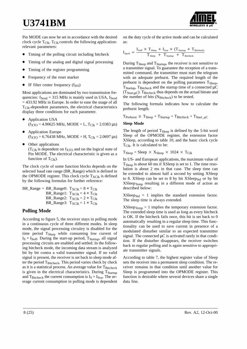
RSense can be connected to VS or GND via a µC or by thedigital output port POUT of the U3741BM receiver IC.The receiver can be switched from full sensitivity toreduced sensitivity or vice versa at any time. In pollingmode, the receiver will not wake up if the RF input signaldoes not exceed the selected sensitivity. If the receiver isalready active, the data stream at Pin DATA will disap-pear when the input signal is lower than defined by thereduced sensitivity. Instead of the data stream, the patternaccording to figure 7 is issued at Pin DATA to indicatethat the receiver is still active.
DATAttmin2 DATA_L_max
Figure 7. Steady L state limited DATA output pattern
FSK/ASK Demodulator and Data Filter
The signal coming from the RSSI amplifier is convertedinto the raw data signal by the ASK/FSK demodulator.The operating mode of the demodulator is set via PinASK/FSK. Logic ‘L’ sets the demodulator to FSK, Logic‘H’ sets it into ASK mode.
In ASK mode an automatic threshold control circuit(ATC) is employed to set the detection reference voltageto a value where a good signal-to-noise ratio is achieved.This circuit also implies the effective suppression of anykind of inband noise signals or competing transmitters.If the S/N ratio exceeds 10 dB, the data signal can be de-tected properly.
The FSK demodulator is intended to be used for an FSKdeviation of f ≥ 20 kHz. Lower values may be used butthe sensitivity of the receiver is reduced in that condition.The minimum usable deviation is dependent on theselected baudrate. In FSK mode, only BR_Range0 andBR_Range1 are available. In FSK mode, the data signalcan be detected if the S/N Ratio exceeds 2 dB.
The output signal of the demodulator is filtered by thedata filter before it is fed into the digital signal processingcircuit. The data filter improves the S/N ratio as its pass-band can be adopted to the characteristics of the datasignal. The data filter consists of a 1st-order highpass anda 1st-order lowpass filter.
The highpass filter cut-off frequency is defined by an ex-ternal capacitor connected to Pin CDEM. The cut-offfrequency of the highpass filter is defined by the follow-ing formula:
fcu_DF 1
2 30 k CDEM
In self-polling mode, the data filter must settle very rap-idly to achieve a low current consumption. Therefore,CDEM cannot be increased to very high values if selfpolling is used. On the other hand, CDEM must be largeenough to meet the data filter requirements according tothe data signal. Recommended values for CDEM aregiven in the electrical characteristics. The values areslightly different for ASK and FSK mode.
The cut-off frequency of the lowpass filter is defined bythe selected baudrate range (BR_Range). BR_Range isdefined in the OPMODE register (refer to chapter ‘Con-figuration of the Receiver’). BR_Range must be set inaccordance to the used baudrate.

U3741BM
Rev. A2, 12-Oct-00 7 (25)
The U3741BMis designed to operate with data codingwhere the DC level of the data signal is 50%. This is validfor Manchester and Bi-phase coding. If other modulationschemes are used, the DC level should always remainwithin the range of VDC_min = 33% and VDC_max = 66%.The sensitivity may be reduced by up to 1.5 dB in thatcondition.
Each BR_Range is also defined by a minimum and a max-imum edge-to-edge time (tee_sig). These limits aredefined in the electrical characteristics. They should notbe exceeded to maintain full sensitivity of the receiver.
Receiving Characteristics
The RF receiver U3741BM can be operated with andwithout a SAW front end filter. In a typical automotive ap-plication, a SAW filter is used to achieve betterselectivity. The selectivity with and without a SAW frontend filter is illustrated in figure 8. This example relates toASK mode and the 300-kHz bandwidth version of theU3741BM. FSK mode and the 600-kHz version of the re-ceiver exhibit similar behavior. Note that the mirrorfrequency is reduced by 40 dB. The plots are printed rela-tively to the maximum sensitivity. If a SAW filter is used,an insertion loss of about 4 dB must be considered.
When designing the system in terms of receiving band-width, the LO deviation must be considered as it alsodetermines the IF center frequency. The total LO devi-ation is calculated to be the sum of the deviation of thecrystal and the XTO deviation of the U3741BM. Low-cost crystals are specified to be within ±100 ppm. TheXTO deviation of the U3741BM is an additional devi-ation due to the XTO circuit. This deviation is specifiedto be ±30 ppm. If a crystal of ±100 ppm is used, the totaldeviation is ±130 ppm in that case. Note that the receivingbandwidth and the IF-filter bandwidth are equivalent inASK mode but not in FSK mode.
–100
–90
–80
–70
–60
–50
–40
–30
–20
–10
0
–6 –5 –4 –3 –2 –1 0 1 2 3 4 5 6
dP (
dB
m )
df ( MHz )
with SAW
without SAW
Figure 8. Receiving frequency response
Polling Circuit and Control Logic
The receiver is designed to consume less than 1 mA whilebeing sensitive to signals from a corresponding transmit-ter. This is achieved via the polling circuit. This circuitenables the signal path periodically for a short time. Dur-ing this time the bitcheck logic verifies the presence of avalid transmitter signal. Only if a valid signal is detectedthe receiver remains active and transfers the data to theconnected µC. If there is no valid signal present, thereceiver is in sleep mode most of the time resulting in lowcurrent consumption. This condition is called pollingmode. A connected µC is disabled during that time.
All relevant parameters of the polling logic can be config-ured by the connected µC. This flexibility enables theuser to meet the specifications in terms of current con-sumption, system response time, data rate etc.
Regarding the number of connection wires to the C, thereceiver is very flexible. It can be either operated by asingle bi-directional line to save ports to the connectedC. Or it can be operated by up to three uni-directionalports.
Basic Clock Cycle of the Digital Circuitry
The complete timing of the digital circuitry and the ana-log filtering is derived from one clock. According tofigure 9, this clock cycle TClk is derived from the crystaloscillator (XTO) in combination with a divider. The divi-sion factor is controlled by the logical state at Pin MODE.According to chapter ‘RF Front End’, the frequency of thecrystal oscillator (fXTO) is defined by the RF input signal(fRFin) which also defines the operating frequency of thelocal oscillator (fLO).
DVCC
XTO
MODE
T
f
16
15
14
Clk
XTO
XTO
Divider:14/:10
L : USA(:10)H: Europe(:14)
Figure 9. Generation of the basic clock cycle
U3741BM
Rev. A2, 12-Oct-008 (25)
Pin MODE can now be set in accordance with the desiredclock cycle TClk. TClk controls the following application-relevant parameters:
Timing of the polling circuit including bitcheck
Timing of the analog and digital signal processing
Timing of the register programming
Frequency of the reset marker
IF filter center frequency (fIF0)
Most applications are dominated by two transmission fre-quencies: fSend = 315 MHz is mainly used in USA, fSend= 433.92 MHz in Europe. In order to ease the usage of allTClk-dependent parameters, the electrical characteristicsdisplay three conditions for each parameter.
Application USA (fXTO = 4.90625 MHz, MODE = L, TClk = 2.0383 µs)
Application Europe (fXTO = 6.76438 MHz, MODE = H, TClk = 2.0697 µs)
Other applications (TClk is dependent on fXTO and on the logical state ofPin MODE. The electrical characteristic is given as afunction of TClk).
The clock cycle of some function blocks depends on theselected baud rate range (BR_Range) which is defined inthe OPMODE register. This clock cycle TXClk is definedby the following formulas for further reference:
BR_Range = BR_Range0: TXClk = 8 × TClkBR_Range1: TXClk = 4 × TClkBR_Range2: TXClk = 2 × TClkBR_Range3: TXClk = 1 × TClk
Polling Mode
According to figure 5, the receiver stays in polling modein a continuous cycle of three different modes. In sleepmode, the signal processing circuitry is disabled for thetime period TSleep while consuming low current ofIS = ISoff. During the start-up period, TStartup, all signalprocessing circuits are enabled and settled. In the follow-ing bitcheck mode, the incoming data stream is analyzedbit by bit contra a valid transmitter signal. If no validsignal is present, the receiver is set back to sleep mode af-ter the period TBitcheck. This period varies check by checkas it is a statistical process. An average value for TBitcheckis given in the electrical characteristics. During TStartupand TBitcheck the current consumption is IS = ISon. The av-erage current consumption in polling mode is dependent
on the duty cycle of the active mode and can be calculatedas:
ISpoll ISoff TSleep ISon (TStartup TBitcheck)
TSleep TStartup TBitcheck
During TSleep and TStartup, the receiver is not sensitive toa transmitter signal. To guarantee the reception of a trans-mitted command, the transmitter must start the telegramwith an adequate preburst. The required length of thepreburst is dependent on the polling parameters TSleep,TStartup, TBitcheck and the startup time of a connected µC(TStart,µC). TBitcheck thus depends on the actual bitrate andthe number of bits (NBitcheck) to be tested.
The following formula indicates how to calculate thepreburst length.
TPreburst TSleep + TStartup + TBitcheck + TStart_C
Sleep Mode
The length of period TSleep is defined by the 5-bit wordSleep of the OPMODE register, the extension factorXSleep, according to table 10, and the basic clock cycleTClk. It is calculated to be:
TSleep = Sleep XSleep 1024 TClk
In US- and European applications, the maximum value ofTSleep is about 60 ms if XSleep is set to 1. The time reso-lution is about 2 ms in that case. The sleep time canbe extended to almost half a second by setting XSleepto 8. XSleep can be set to 8 by bit XSleepStd or by bitXSleepTemp resulting in a different mode of action asdescribed below:
XSleepStd = 1 implies the standard extension factor.The sleep time is always extended.
XSleepTemp = 1 implies the temporary extension factor.The extended sleep time is used as long as every bitcheckis OK. If the bitcheck fails once, this bit is set back to 0automatically resulting in a regular sleep time. This func-tionality can be used to save current in presence of amodulated disturber similar to an expected transmittersignal. The connected µC is activated rarely in that condi-tion. If the disturber disappears, the receiver switchesback to regular polling and is again sensitive to appropri-ate transmitter signals.
According to table 7, the highest register value of Sleepsets the receiver into a permanent sleep condition. The re-ceiver remains in that condition until another value forSleep is programmed into the OPMODE register. Thisfunction is desirable where several devices share a singledata line.

U3741BM
Rev. A2, 12-Oct-00 9 (25)
Sleep mode:All circuits for signal processing aredisabled. Only XTO and Pollinglogic are enabled.IS = ISoffTSleep = Sleep × XSleep × 1024 × TClk
Start-up mode:The signal processing circuits areenabled. After the start-up time(TStartup) all circuits are in stablecondition and ready to receive.IS = ISonTStartup
Bitcheck mode:The incomming data stream isanalyzed. If the timing indicates avalid transmitter signal, the receiver isset to receiving mode. Otherwise it isset to Sleep mode.IS = ISonTBitcheck
Receiving mode:The receiver is turned on permanentlyand passes the data stream to theconnected C. It can be set to Sleepmode through an OFF command viaPin DATA or ENABLE.IS = ISon
BitcheckOK ?
OFF command
Sleep: 5-bit word defined by Sleep0 to Sleep4 in OPMODE register
XSleep: Extension factor defined by XSleepStd and XSleepTemp according to table 8
TClk: Basic clock cycle defined by fXTO and Pin MODE
TStartup: Is defined by the selected baud rate range and TClk. The baud rate rangeis defined by Baud0 and Baud1 in the OPMODE register.
TBitcheck: Depends on the result of the bitcheck
If the bitcheck is ok, TBitcheck depends on the number of bits to bechecked (NBitcheck) and on the utilized data rate.
If the bitcheck fails, the average time period for that check depends on the selected baud rate range and on TClk. The baud rate range is defined by Baud0 and Baud1 in the OPMODE register.
NO
YES
Figure 10. Polling mode flow chart
Bitcheck
Enable IC
DATA
1/2 Bit
Polling – Mode
( Number of checked Bits: 3 )Bitcheck ok
1/2 Bit 1/2 Bit 1/2 Bit 1/2 Bit 1/2 Bit
Receiving mode
Dem_out
Figure 11. Timing diagram for complete sucessful bitcheck

U3741BM
Rev. A2, 12-Oct-0010 (25)
Bitcheck Mode
In bitcheck mode, the incoming data stream is examinedto distinguish between a valid signal from a correspond-ing transmitter and signals due to noise. This is done bysubsequent time frame checks where the distances be-tween 2 signal edges are continuously compared to aprogrammable time window. The maximum count of thisedge-to-edge tests before the receiver switches to receiv-ing mode is also programmable.
Configuring the Bitcheck
Assuming a modulation scheme that contains 2 edges perbit, two time frame checks are verifying one bit. This isvalid for Manchester, Bi-phase and most other modula-tion schemes. The maximum count of bits to be checkedcan be set to 0, 3, 6 or 9 bits via the variable NBitcheck inthe OPMODE register. This implies 0, 6, 12 and 18 edge-to-edge checks respectively. If NBitcheck is set to a highervalue, the receiver is less likely to switch to receivingmode due to noise. In the presence of a valid transmittersignal, the bitcheck takes less time if NBitcheck is set to alower value. In polling mode, the bitcheck time is not de-pendent on NBitcheck. Figure 11 shows an example where3 bits are tested successfully and the data signal is trans-ferred to Pin DATA.
According to figure 12, the time window for the bitcheckis defined by two separate time limits. If the edge-to-edgetime tee is in between the lower bitcheck limit TLim_minand the upper bitcheck limit TLim_max, the check will becontinued. If tee is smaller than TLim_min or tee exceedsTLim_max, the bitcheck will be terminated and the receiverswitches to sleep mode.
Dem_outt ee
TLim_min
TLim_max
1/fSig
Figure 12. Valid time window for bitcheck
For best noise immunity it is recommended to use a lowspan between TLim_min and TLim_max. This is achievedusing a fixed frequency at a 50% duty cycle for the trans-mitter preburst. A ‘11111...’ or a ‘10101...’ sequence inManchester or Bi-phase is a good choice concerning thatadvice. A good compromise between receiver sensitivityand susceptibility to noise is a time window of ± 25% re-garding the expected edge-to-edge time tee. Usingpre-burst patterns that contain various edge-to-edge timeperiods, the bitcheck limits must be programmed accord-ing to the required span.
The bitcheck limits are determined by means of the for-mula below:
TLim_min = Lim_min × TXClkTLim_max = (Lim_max –1) × TXClk
Lim_min and Lim_max are defined by a 5-bit word eachwithin the LIMIT register.
Using above formulas, Lim_min and Lim_max can be de-termined according to the required TLim_min, TLim_maxand TXClk. The time resolution when defining TLim_minand TLim_max is TXClk. The minimum edge-to-edge timetee (tDATA_L_min, tDATA_H_min) is defined according to thechapter ‘Receiving Mode’. Due to this, the lower limitshould be set to Lim_min ≥ 10. The maximum value ofthe upper limit is Lim_max = 63.
Figures 13, 14 and 15 illustrate the bitcheck for the defaultbitcheck limits Lim_min = 14 and Lim_max = 24. Whenthe IC is enabled, the signal processing circuits areenabled during TStartup. The output of the ASK/ FSKdemodulator (Dem_out) is undefined during that period.When the bitcheck becomes active, the bitcheck counteris clocked with the cycle TXClk.
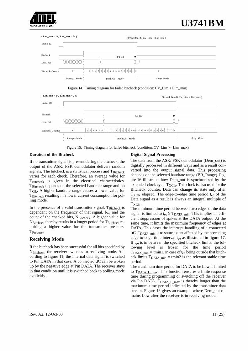
Figure 13 shows how the bitcheck proceeds if the bit-check counter value CV_Lim is within the limits definedby Lim_min and Lim_max at the occurrence of a signaledge. In figure 14, the bitcheck fails as the value CV_limis lower than the limit Lim_min. The bitcheck also failsif CV_Lim reaches Lim_max. This is illustrated in fig-ure 15.
Bitcheck
Enable IC
Dem_out
Bitcheck–Counter 0 2 3 4 5 6 2 4 51 7 8 1 3 6 7 8 9 11 12 13 1410
1/2 Bit
15 16 17 18 1 2 3 4 5 6
( Lim_min = 14, Lim_max = 24 )
7 8 9 10 11 12 13 14 15 1 2 3 4
1/2 Bit 1/2 Bit
Bitcheck ok Bitcheck ok
TStartup
TXClk
Figure 13. Timing diagram during bitcheck
U3741BM
Rev. A2, 12-Oct-00 11 (25)
Bitcheck
Enable IC
Bitcheck–Counter 0 2 3 4 5 6 2 4 51 1 3 6 7 8 9 11 1210
1/2 Bit
Startup – Mode
0
( Lim_min = 14, Lim_max = 24 )
Sleep–Mode
Bitcheck failed ( CV_Lim < Lim_min )
Dem_out
Bitcheck – Mode
Figure 14. Timing diagram for failed bitcheck (condition: CV_Lim < Lim_min)
Bitcheck
Enable IC
Bitcheck–Counter 0 2 3 4 5 6 2 4 51 7 3 6 7 8 9 11 1210
1/2 Bit
Startup – Mode
20
( Lim_min = 14, Lim_max = 24 )
Sleep–Mode
Bitcheck failed ( CV_Lim = Lim_max )
13 14 15 16 17 18 19 21 22 23 24 01
Dem_out
Bitcheck – Mode
Figure 15. Timing diagram for failed bitcheck (condition: CV_Lim >= Lim_max)
Duration of the Bitcheck
If no transmitter signal is present during the bitcheck, theoutput of the ASK/ FSK demodulator delivers randomsignals. The bitcheck is a statistical process and TBitcheckvaries for each check. Therefore, an average value forTBitcheck is given in the electrical characteristics.TBitcheck depends on the selected baudrate range and onTClk. A higher baudrate range causes a lower value forTBitcheck resulting in a lower current consumption for pol-ling mode.
In the presence of a valid transmitter signal, TBitcheck isdependant on the frequency of that signal, fSig and thecount of the checked bits, NBitcheck. A higher value forNBitcheck thereby results in a longer period for TBitcheck re-quiring a higher value for the transmitter pre-burstTPreburst.
Receiving Mode
If the bitcheck has been successful for all bits specified byNBitcheck, the receiver switches to receiving mode. Ac-cording to figure 11, the internal data signal is switchedto Pin DATA in that case. A connected µC can be wokenup by the negative edge at Pin DATA. The receiver staysin that condition until it is switched back to polling modeexplicitly.
Digital Signal ProcessingThe data from the ASK/ FSK demodulator (Dem_out) isdigitally processed in different ways and as a result con-verted into the output signal data. This processingdepends on the selected baudrate range (BR_Range). Fig-ure 16 illustrates how Dem_out is synchronized by theextended clock cycle TXClk. This clock is also used for theBitcheck counter. Data can change its state only afterTXClk elapsed. The edge-to-edge time period tee of theData signal as a result is always an integral multiple ofTXClk.The minimum time period between two edges of the datasignal is limited to tee ≥ TDATA_min. This implies an effi-cient suppression of spikes at the DATA output. At thesame time, it limits the maximum frequency of edges atDATA. This eases the interrupt handling of a connectedµC. TDATA_min is to some extent affected by the precedingedge-to-edge time interval tee as illustrated in figure 17.If tee is in between the specified bitcheck limits, the fol-lowing level is frozen for the time periodTDATA_min = tmin1, in case of tee being outside that bitch-eck limits TDATA_min = tmin2 is the relevant stable timeperiod.The maximum time period for DATA to be Low is limitedto TDATA_L_max. This function ensures a finite responsetime during programming or switching off the receivervia Pin DATA. TDATA_L_max is thereby longer than themaximum time period indicated by the transmitter datastream. Figure 18 gives an example where Dem_out re-mains Low after the receiver is in receiving mode.

U3741BM
Rev. A2, 12-Oct-0012 (25)
Clock Bitcheckcounter
DATA
T
Dem_out
XClk
t ee
Figure 16. Synchronization of the demodulator output
DATA
tmin1
CV_Lim < Lim_min or CV_Lim ≥ Lim_max
Lim_min ≤ CV_Lim < Lim_max
Dem_out
tee
tee
tmin2
Figure 17. Debouncing of the demodulator output
Bitcheck
Enable IC
DATA
Sleep – Mode Receiving modet
tmin2Bitcheck – ModeDATA_L_max
Dem_out
Figure 18. Steady L state limited DATA output pattern after transmission
After the end of a data transmission, the receiver remainsactive and random noise pulses appear at Pin DATA. Theedge-to-edge time period tee of the majority of these noisepulses is equal to or slightly higher than TDATA_min.
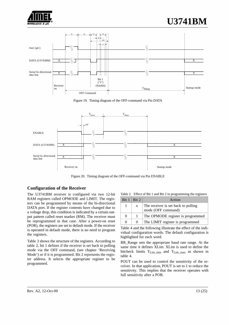
Switching the Receiver Back to Sleep Mode
The receiver can be set back to polling mode via PinDATA or via Pin ENABLE.
When using Pin DATA, this pin must be pulled to Low forthe period t1 by the connected µC. Figure 19 illustratesthe timing of the OFF command (see also figure 23). Theminimum value of t1 depends on BR_Range. The maxi-mum value for t1 is not limited but it is recommended notto exceed the specified value to prevent erasing the resetmarker. This item is explained in more detail in the chap-ter ‘Configuration of the Receiver’. Setting the receiverto sleep mode via DATA is achieved by programming bit
1 of the OPMODE register to be ‘1’. Only one sync pulse(t3) is issued.
The duration of the OFF command is determined by thesum of t1, t2 and t10. After the OFF command, the sleeptime TSleep elapses. Note that the capacitive load at PinDATA is limited. The resulting time constant togetherwith an optional extenal pull-up resistor may not beexceeded to ensure proper operation.
If the receiver is set to polling mode via Pin ENABLE, an‘L’ pulse (TDoze) must be issued at that pin. Figure 20illustrates the timing of that command. After the positiveedge of this pulse the sleep time TSleep elapses. Thereceiver remains in sleep mode as long as ENABLE isheld to ‘L’. If the receiver is polled exclusively by a µC,TSleep can be programmed to 0 to enable a instantaneousresponse time. This command is the faster option than viaPin DATA at the cost of an additional connection to theµC.
U3741BM
Rev. A2, 12-Oct-00 13 (25)
Out1 (µC)
DATA (U3741BM)
Serial bi–directionaldata line
X
Bit 1(”1”)
X
t1 t2 t3
t4
t5
t7
X
X
(Startbit)Startup mode
OFF Command
TReceiveron
t10
Sleep
Figure 19. Timing diagram of the OFF-command via Pin DATA
ENABLE
DATA (U3741BM)
Serial bi–directionaldata line
X
X
X
Sleep
X
toff
Receiver on Startup mode
TDozeT
Figure 20. Timing diagram of the OFF-command via Pin ENABLE
Configuration of the ReceiverThe U3741BM receiver is configured via two 12-bitRAM registers called OPMODE and LIMIT. The regis-ters can be programmed by means of the bi-directionalDATA port. If the register contents have changed due toa voltage drop, this condition is indicated by a certain out-put pattern called reset marker (RM). The receiver mustbe reprogrammed in that case. After a power-on reset(POR), the registers are set to default mode. If the receiveris operated in default mode, there is no need to programthe registers.
Table 3 shows the structure of the registers. According totable 2, bit 1 defines if the receiver is set back to pollingmode via the OFF command, (see chapter ‘ReceivingMode’) or if it is programmed. Bit 2 represents the regis-ter address. It selects the appropriate register to beprogrammed.
Table 2. Effect of Bit 1 and Bit 2 in programming the registers
Bit 1 Bit 2 Action
1 x The receiver is set back to pollingmode (OFF command)
0 1 The OPMODE register is programmed
0 0 The LIMIT register is programmed
Table 4 and the following illustrate the effect of the indi-vidual configuration words. The default configuration ishighlighted for each word.
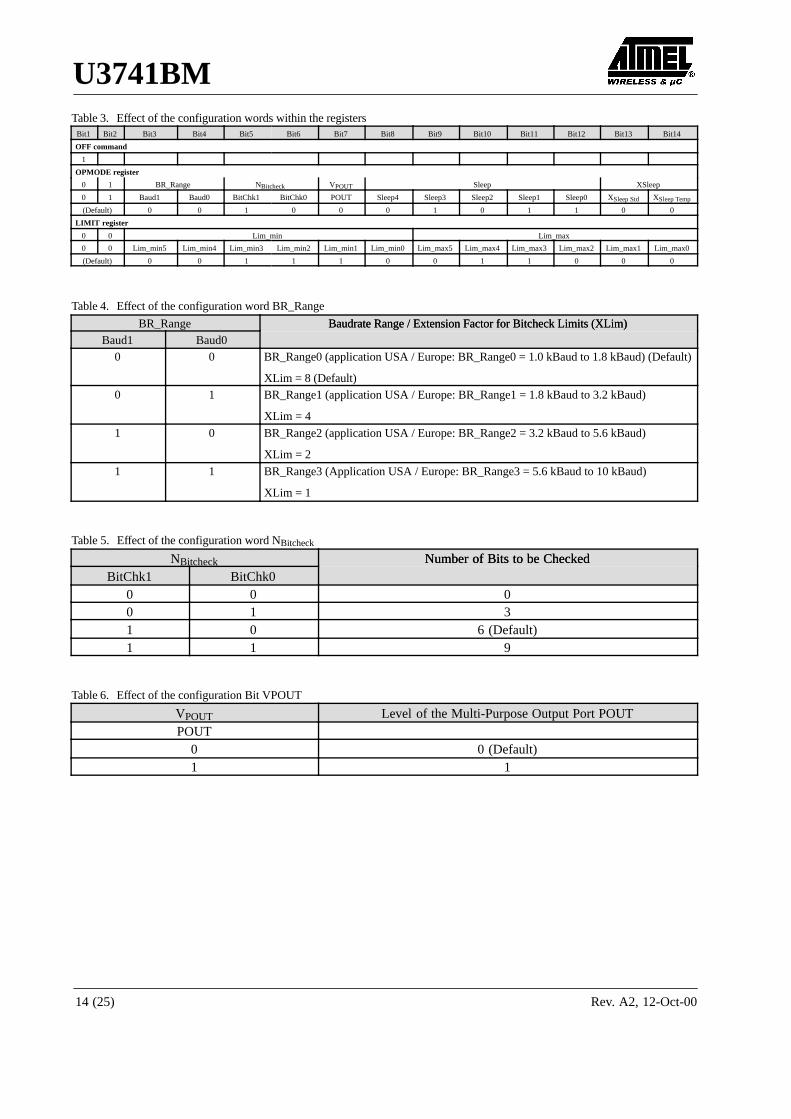
BR_Range sets the appropriate baud rate range. At thesame time it defines XLim. XLim is used to define thebitcheck limits TLim_min and TLim_max as shown intable 4.
POUT can be used to control the sensitivity of the re-ceiver. In that application, POUT is set to 1 to reduce thesensitivity. This implies that the receiver operates withfull sensitivity after a POR.
U3741BM
Rev. A2, 12-Oct-0014 (25)
Table 3. Effect of the configuration words within the registersBit1 Bit2 Bit3 Bit4 Bit5 Bit6 Bit7 Bit8 Bit9 Bit10 Bit11 Bit12 Bit13 Bit14
OFF command
1
OPMODE register
0 1 BR_Range NBitcheck VPOUT Sleep XSleep
0 1 Baud1 Baud0 BitChk1 BitChk0 POUT Sleep4 Sleep3 Sleep2 Sleep1 Sleep0 XSleep Std XSleep Temp
(Default) 0 0 1 0 0 0 1 0 1 1 0 0
LIMIT register
0 0 Lim_min Lim_max
0 0 Lim_min5 Lim_min4 Lim_min3 Lim_min2 Lim_min1 Lim_min0 Lim_max5 Lim_max4 Lim_max3 Lim_max2 Lim_max1 Lim_max0
(Default) 0 0 1 1 1 0 0 1 1 0 0 0
Table 4. Effect of the configuration word BR_Range
BR_Range Baudrate Range / Extension Factor for Bitcheck Limits (XLim)Baud1 Baud0
Baudrate Range / Extension Factor for Bitcheck Limits (XLim)
0 0 BR_Range0 (application USA / Europe: BR_Range0 = 1.0 kBaud to 1.8 kBaud) (Default)
XLim = 8 (Default)0 1 BR_Range1 (application USA / Europe: BR_Range1 = 1.8 kBaud to 3.2 kBaud)
XLim = 4
1 0 BR_Range2 (application USA / Europe: BR_Range2 = 3.2 kBaud to 5.6 kBaud)
XLim = 2
1 1 BR_Range3 (Application USA / Europe: BR_Range3 = 5.6 kBaud to 10 kBaud)
XLim = 1
Table 5. Effect of the configuration word NBitcheck
NBitcheck Number of Bits to be CheckedBitChk1 BitChk0
Number of Bits to be Checked
0 0 00 1 31 0 6 (Default)1 1 9
Table 6. Effect of the configuration Bit VPOUT
VPOUT Level of the Multi-Purpose Output Port POUTPOUT
0 0 (Default)1 1

U3741BM
Rev. A2, 12-Oct-00 15 (25)
Table 7. Effect of the configuration word SleepSleep Start Value for Sleep Counter (TSleep = Sleep × Xsleep × 1024 × TClk)
Sleep4 Sleep3 Sleep2 Sleep1 Sleep0
0 0 0 0 0 0 (Receiver is continuously polling until a valid signal occurs)
0 0 0 0 1 1 (TSleep ≈ 2ms for XSleep =1 in US- / European applications)
0 0 0 1 0 2
0 0 0 1 1 3
.
.
.
.
.
.
.
.
.
.
.
.
.
.
.
.
.
.
0 1 0 1 1 11 (USA: TSleep = 22.96 ms, Europe: TSleep = 23.31 ms) (Default)
.
.
.
.
.
.
.
.
.
.
.
.
.
.
.
.
.
.
1 1 1 0 1 29
1 1 1 1 0 30
1 1 1 1 1 31 (Permanent sleep mode)
Table 8. Effect of the configuration word XSleep
XSleep Extension Factor for Sleep Time (TSleep = Sleep × Xsleep × 1024 × TClk)XSleepStd XSleepTemp
Extension Factor for Sleep Time (TSleep = Sleep × Xsleep × 1024 × TClk)
0 0 1 (Default)0 1 8 (XSleep is reset to 1 if bitcheck fails once)1 0 8 (XSleep is set permanently)1 1 8 (XSleep is set permanently)
Table 9. Effect of the configuration word Lim_min
Lim_min Lower Limit Value for BitcheckLim_min < 10 is not applicable (TLim_min = Lim_min × XLim × TClk)
0 0 1 0 1 0 100 0 1 0 1 1 110 0 1 1 0 0 120 0 1 1 0 1 130 0 1 1 1 0 14 (Default)
(USA: TLim_min = 228 µs, Europe: TLim_min = 232 µs)
.
.
.
.
.
.
.
.
.
.
.
.
.
.
.
.
.
.
1 1 1 1 0 1 611 1 1 1 1 0 621 1 1 1 1 1 63

U3741BM
Rev. A2, 12-Oct-0016 (25)
Table 10. Effect of the configuration word Lim_max
Lim_max Upper Limit Value for BitcheckLim_max < 12 is not applicable (TLim_max = (Lim_max –1) × XLim × TClk)
0 0 1 1 0 0 120 0 1 1 0 1 130 0 1 1 1 0 14.
.
.
.
.
.
.
.
.
.
.
.
.
.
.
.
.
.
0 1 1 0 0 0 24 (Default)
(USA: TLim_max = 375 µs, Europe: TLim_max = 381 µs)
.
.
.
.
.
.
.
.
.
.
.
.
.
.
.
.
.
.
1 1 1 1 0 1 611 1 1 1 1 0 621 1 1 1 1 1 63
Conservation of the Register Information
The U3741BM has an integrated power-on reset andbrown–out detection circuitry to provide a mechanism topreserve the RAM register information.
According to figure 21, a power-on reset (POR) is gener-ated if the supply voltage VS drops below the thresholdvoltage VThReset. The default parameters are pro-grammed into the configuration registers in thatcondition. Once VS exceeds VThReset, the POR iscanceled after the minimum reset period tRst. A POR isalso generated when the supply voltage of the receiver isturned on.
To indicate that condition, the receiver displays a resetmarker (RM) at Pin DATA after a reset. The RM is repre-
sented by the fixed frequency fRM at a 50% duty cycle.RM can be canceled via an ‘L’ pulse t1 at Pin DATA. TheRM implies the following characteristics:
fRM is lower than the lowest feasible frequency of adata signal. By this means, RM cannot be misinter-preted by the connected µC.
If the receiver is set back to polling mode via pinDATA, RM cannot be canceled by accident if t1 is ap-plied according to the proposal in the section‘Programming the configuration registers’.
By means of that mechanism, the receiver cannot lose itsregister information without communicating that condi-tion via the reset marker RM.
V
POR
DATA (U3741BM) X
1 / f
t
SVThReset
Rst
RM
Figure 21. Generation of the power on reset

U3741BM
Rev. A2, 12-Oct-00 17 (25)
Out1 (mC)
DATA (U3741BM)
Serial bi–directionaldata line
X
Bit 1(”0”)
Bit 2(”1”)
Bit 13(”0”)
Bit 14(”1”)
X
t1 t2 t3
t4
t5
t6t8
t7
X
X
T
Programming Frame
(Startbit) (Register– select)
(Poll8) (Poll8R)Receiveron
Startupmode
t9 Sleep
Figure 22. Timing of the register programming
Programming the Configuration Register
The configuration registers are programmed serially viathe bi-directional data line according to figure 22 and fig-ure 23.
U3741BM
internal pull-upresistor
DATA I/O
C
Out1 ( C)
bi-directionaldata-line
Data (U3741BM)
Figure 23. One-wire connection to a C
To start programming, the serial data line DATA is pulledto ‘L’ for the time period t1 by the µC. When DATA hasbeen released, the receiver becomes the master device.When the programming delay period t2 has elapsed, itemits 14 subsequent synchronization pulses with thepulse length t3. After each of these pulses, a programmingwindow occurs. The delay until the program windowstarts is determined by t4, the duration is defined by t5.Within the programming window, the individual bits areset. If the µC pulls down Pin DATA for the time period t7during t5, the according bit is set to ‘0’. If no program-ming pulse t7 is issued, this bit is set to ‘1’. All 14 bits aresubsequently programmed in this way. The time frame toprogram a bit is defined by t6.
Bit 14 is followed by the equivalent time window t9. Dur-ing this window, the equivalent acknowledge pulse t8(E_Ack) occurs if the just programmed modeword isequivalent to the modeword that was already stored inthat register. E_Ack should be used to verify that the mo-deword was correctly transferred to the register. Theregister must be programmed twice in that case.
Programming of a register is possible both during sleep–and active mode of the receiver.
During programming, the LNA, LO, lowpass filter, IF-amplifier and the FSK/ASK Manchester demodulator aredisabled.
The programming start pulse t1 initiates the program-ming of the configuration registers. If bit 1 is set to ‘1’, itrepresents the OFF-command to set the receiver back topolling mode at the same time. For the length of the pro-gramming start pulse t1, the following convention shouldbe considered:
t1(min) < t1 < 1535 × TClk: [t1(min) is the minimumspecified value for the relevant BR_Range]
Programming (respectively OFF-command) is initiated ifthe receiver is not in reset mode. If the receiver is in resetmode programming (respectively Off-command) is notinitiated, and the reset marker RM is still present at PinDATA.
This period is generally used to switch the receiver topolling mode. In a reset condition, RM is not canceled byaccident.
t1 > 5632 × TClk
Programming (respectively OFF-command) is initiatedin any case. RM is canceled if present.
This period is used if the connected µC detected RM. Ifa configuration register is programmed, this time periodfor t1 can generally be used.
Note that the capacitive load at Pin DATA is limited.The resulting time constant t together with an optionalexternal pull-up resistor may not be exceeded to ensureproper operation.

U3741BM
Rev. A2, 12-Oct-0018 (25)
Absolute Maximum RatingsParameters Symbol Min. Typ. Max. Unit
Supply voltage VS 6 VPower dissipation Ptot 450 mWJunction temperature Tj 150 °CStorage temperature Tstg –55 +125 °CAmbient temperature Tamb –40 +105 °CMaximum input level, input matched to 50 Pin_max 10 dBm
Thermal ResistanceParameters Symbol Value Unit
Junction ambient RthJA 100 K/W
Electrical CharacteristicsAll parameters refer to GND, Tamb = –40°C to +105°C, VS = 4.5 V to 5.5 V, f0 = 433.92 MHz and f0 = 315 MHz, un-less otherwise specified. (VS = 5 V, Tamb = 25°C)
Parameter Test Condition Symbol 6.76438 MHz Osc.(MODE: 1)
4.90625 MHz Osc.(MODE: 0)
Variable Oscillator Unit
Min. Typ. Max. Min. Typ. Max. Min. Typ. Max.
Basic clock cycle of the digital circuitry
Basic clockcycle
MODE = 0 (USA)MODE = 1 (Europe)
TClk2.0697
2.0383 1/(fxto/10)1/(fxto/14)
µsµs
Extendedbasic clockcycle
BR_Range0BR_Range1BR_Range2BR_Range3
TXClk 16.68.34.12.1
16.38.24.12.0
8 × TClk4 × TClk2 × TClk1 × TClk
µsµsµsµs
Polling mode
Sleep time Sleep and XSleepare defined in theOPMODE register
TSleep Sleep ×XSleep ×1024 ×2.0697
Sleep ×XSleep ×1024 ×2.0383
Sleep ×XSleep ×1024 ×
TClk
ms
Start-uptime
BR_Range0BR_Range1BR_Range2BR_Range3
TStartup 185510611061663
182710451045653
896.5512.5512.5320.5× TClk
µsµsµsµsµs
Time forBitcheck
Average bitchecktime while pollingBR_Range0BR_Range1BR_Range2BR_Range3
TBitcheck
0.450.240.140.14
0.470.260.160.15
msmsmsms
Bitcheck time for avalid input signalfSigNBitcheck = 0NBitcheck = 3NBitcheck = 6NBitcheck = 9
TBitcheck
3/fSig6/fSig9/fSig
3.5/fSig6.5/fSig9.5/fSig
3/fSig6/fSig9/fSig
3.5/fSig6.5/fSig9.5/fSig
TXClk3.5/fSig6.5/fSig9.5/fSig
msmsmsms
Receiving mode
Intermediatefrequency MODE=0 (USA)
MODE=1 (Europe)
fIF
1.01.0 fXTO × 64 / 314
fXTO × 64 / 432.92MHzMHz
Baud raterange
BR_Range0BR_Range1BR_Range2BR_Range3
BR_Range 1.01.83.25.6
1.83.25.6
10.0
1.01.83.25.6
1.83.25.6
10.0
BR_Range0 × 2 µs / TClk BR_Range1 × 2 µs / TClkBR_Range2 × 2 µs / TClkBR_Range3 × 2 µs / TClk
kBaudkBaudkBaudkBaud

U3741BM
Rev. A2, 12-Oct-00 19 (25)
Electrical Characteristics (continued)All parameters refer to GND, Tamb = –40°C to +105°C, VS = 4.5 V to 5.5 V, f0 = 433.92 MHz and f0 = 315 MHz, un-less otherwise specified. (VS = 5 V, Tamb = 25°C)
Parameter Test Condition Symbol 6.76438 MHz Osc.(MODE: 1)
4.90625 MHz Osc.(MODE: 0)
Variable Oscillator Unit
Min. Typ. Max. Min. Typ. Max. Min. Typ. Max.
Receiving mode (continued)
Minimumtime periodbetween edgesat Pin DATA(figure 17)
BR_Range0
BR_Range1
BR_Range2
BR_Range3
TDATA_mintmin1tmin2tmin1tmin2tmin1tmin2tmin1tmin2
1491827591
37.345.518.622.8
1471797390
36.744.818.322.4
9 × TXClk11 × TXCl9 × TXClk11 × TXClk9 × TXClk11 × TXClk9 × TXClk11 × TXClk
µsµsµsµsµsµsµsµs
Maximumlow period atDATA(figure 18)
BR_Range0BR_Range1BR_Range2BR_Range3
TDATA_L_
max
21691085542271
21361068534267
131 × TXClk
131 × TXClk131 × TXClk
131 × TXClk
µsµsµsµs
OFF com-mand at PinENABLE(figure 20)
tDoze 3.1 3.05 1.5 × TClk µs
Configuration of the receiver
Frequency ofthe resetmarker(figure 21)
fRM 117.9 119.81
4096 TClk
Hz
Programmingstart pulse(figure 19,figure 22)
BR_Range0BR_Range1BR_Range2BR_Range3after POR
t1 21881104561290
11656
3176317631763176
21551087553286
11479
3128312831283128
1057 × TClk533 × TClk271 × TClk140 × TClk5632 × TClk
1535 × TClk1535 × TClk1535 × TClk1535 × TClk
µs
Programmingdelay period(figure 19,figure 22)
t2 795 798 783 786 384.5 ×TClk
385.5 ×TClk
µs
Synchroni–zation pulse(figure 19,figure 22)
t3 265 261 128 × TClk µs
Delay untilthe programwindow starts(figure 19,figure 22)
t4 131 129 63.5 × TClk µs
Programmingwindow(figure 19,figure 22)
t5 530 522 256 × TClk µs
Time frameof a bit(figure 22)
t6 1060 1044 512 × TClk µs
Programmingpulse(figure 19,figure 22)
t7 133 529 131 521 64 × TClk 256 × TClk µs
Equivalentacknowledgepulse: E_Ack(figure 22)
t8 265 261 128 × TClk µs
Equivalenttime window(figure 22)
t9 534 526 258 × TClk µs
OFF-bit pro-grammingwindow(figure 19)
t10 930 916 449.5 ×TClk
µs

U3741BM
Rev. A2, 12-Oct-0020 (25)
Electrical Characteristics (continued)All parameters refer to GND, Tamb = –40°C to +105°C, VS = 4.5 V to 5.5 V, f0 = 433.92 MHz and f0 = 315 MHz, un-less otherwise specified. (VS = 5 V, Tamb = 25°C)
Parameters Test Conditions / Pins Symbol Min. Typ. Max. UnitÁÁÁÁÁÁÁÁÁÁÁÁÁÁÁÁÁÁÁÁÁÁÁÁ
Current consumptionÁÁÁÁÁÁÁÁÁÁÁÁÁÁÁÁÁÁÁÁÁÁÁÁÁÁÁ
Sleep mode(XTO and polling logic active)
ÁÁÁÁÁÁÁÁÁ
ISoffÁÁÁÁÁÁÁÁÁÁÁÁ
ÁÁÁÁÁÁÁÁÁÁÁÁÁÁÁ
190ÁÁÁÁÁÁÁÁÁÁÁÁ
276ÁÁÁÁÁÁÁÁÁÁÁÁ
µA
ÁÁÁÁÁÁÁÁÁÁÁÁÁÁÁÁÁÁÁÁÁÁÁÁ
ÁÁÁÁÁÁÁÁÁÁÁÁÁÁÁÁÁÁÁÁÁÁÁÁÁÁÁ
IC active (startup-, bitcheck-, receivingmode) Pin DATA = H
ÁÁÁÁÁÁÁÁÁ
ISonÁÁÁÁÁÁÁÁÁÁÁÁ
ÁÁÁÁÁÁÁÁÁÁÁÁÁÁÁ
7.0 ÁÁÁÁÁÁÁÁÁÁÁÁ
8.6 ÁÁÁÁÁÁÁÁÁÁÁÁ
mA
ÁÁÁÁÁÁÁÁÁÁÁÁÁÁÁÁÁÁÁÁÁÁÁÁÁÁÁÁÁÁÁÁÁÁÁÁÁÁÁÁÁÁÁÁÁÁÁÁÁÁÁÁÁÁÁÁÁÁÁÁÁÁÁÁ
LNA mixerÁÁÁÁÁÁÁÁÁÁÁÁÁÁÁÁÁÁÁÁÁÁÁÁÁÁÁÁÁÁÁÁ
Third-order intercept pointÁÁÁÁÁÁÁÁÁÁÁÁÁÁÁÁÁÁÁÁÁÁÁÁÁÁÁÁÁÁÁÁÁÁÁÁ
LNA/ mixer/ IF amplifierinput matched according to fig-ure 6
ÁÁÁÁÁÁÁÁÁÁÁÁ
IIP3ÁÁÁÁÁÁÁÁÁÁÁÁÁÁÁÁ
ÁÁÁÁÁÁÁÁÁÁÁÁÁÁÁÁÁÁÁÁ
–28ÁÁÁÁÁÁÁÁÁÁÁÁÁÁÁÁ
ÁÁÁÁÁÁÁÁÁÁÁÁÁÁÁÁ
dBm
ÁÁÁÁÁÁÁÁÁÁÁÁÁÁÁÁÁÁÁÁÁÁÁÁ
LO spurious emission@ RFIn
ÁÁÁÁÁÁÁÁÁÁÁÁÁÁÁÁÁÁÁÁÁÁÁÁÁÁÁ
Input matched according to fig-ure 6, required according toI–ETS 300220
ÁÁÁÁÁÁÁÁÁ
ISLORFÁÁÁÁÁÁÁÁÁÁÁÁ
ÁÁÁÁÁÁÁÁÁÁÁÁÁÁÁ
–73 ÁÁÁÁÁÁÁÁÁÁÁÁ
–57 ÁÁÁÁÁÁÁÁÁÁÁÁ
dBm
ÁÁÁÁÁÁÁÁÁÁÁÁÁÁÁÁ
Noise figure LNA and mixer(DSB)
ÁÁÁÁÁÁÁÁÁÁÁÁÁÁÁÁÁÁ
Input matching according to fig-ure 6
ÁÁÁÁÁÁ
NFÁÁÁÁÁÁÁÁ
ÁÁÁÁÁÁÁÁÁÁ
7 ÁÁÁÁÁÁÁÁ
ÁÁÁÁÁÁÁÁ
dB
ÁÁÁÁÁÁÁÁÁÁÁÁÁÁÁÁÁÁÁÁÁÁÁÁ
LNA_IN input impedanceÁÁÁÁÁÁÁÁÁÁÁÁÁÁÁÁÁÁÁÁÁÁÁÁÁÁÁ
@ 433.92 MHz@ 315 MHz
ÁÁÁÁÁÁÁÁÁ
ZiLNA_IN
ÁÁÁÁÁÁÁÁÁÁÁÁ
ÁÁÁÁÁÁÁÁÁÁÁÁÁÁÁ
1.0 || 1.561.3 || 1.0
ÁÁÁÁÁÁÁÁÁÁÁÁ
ÁÁÁÁÁÁÁÁÁÁÁÁ
kΩ || pFkΩ || pF
ÁÁÁÁÁÁÁÁÁÁÁÁÁÁÁÁÁÁÁÁÁÁÁÁ
1 dB compression point(LNA, mixer, IF amplifier)
ÁÁÁÁÁÁÁÁÁÁÁÁÁÁÁÁÁÁÁÁÁÁÁÁÁÁÁ
Input matched according to fig-ure 6, referred to RFin
ÁÁÁÁÁÁÁÁÁ
IP1dbÁÁÁÁÁÁÁÁÁÁÁÁ
ÁÁÁÁÁÁÁÁÁÁÁÁÁÁÁ
–40 ÁÁÁÁÁÁÁÁÁÁÁÁ
ÁÁÁÁÁÁÁÁÁÁÁÁ
dBm
ÁÁÁÁÁÁÁÁÁÁÁÁÁÁÁÁÁÁÁÁÁÁÁÁÁÁÁÁÁÁÁÁ
Maximum input level ÁÁÁÁÁÁÁÁÁÁÁÁÁÁÁÁÁÁÁÁÁÁÁÁÁÁÁÁÁÁÁÁÁÁÁÁ
Input matched according to fig-ure 6, BER ≤ 10–3,FSK modeASK mode
ÁÁÁÁÁÁÁÁÁÁÁÁ
Pin_maxÁÁÁÁÁÁÁÁÁÁÁÁÁÁÁÁ
ÁÁÁÁÁÁÁÁÁÁÁÁÁÁÁÁÁÁÁÁ
ÁÁÁÁÁÁÁÁÁÁÁÁÁÁÁÁ
–28–20
ÁÁÁÁÁÁÁÁÁÁÁÁÁÁÁÁ
dBmdBm
ÁÁÁÁÁÁÁÁÁÁÁÁÁÁÁÁÁÁÁÁÁÁÁÁÁÁÁÁÁÁÁÁÁÁÁÁÁÁÁÁÁÁÁÁÁÁÁÁÁÁÁÁÁÁÁÁÁÁÁÁÁÁÁÁ
Local oscillator
ÁÁÁÁÁÁÁÁÁÁÁÁÁÁÁÁ
Operating frequency rangeVCO
ÁÁÁÁÁÁÁÁÁÁÁÁÁÁÁÁÁÁ
ÁÁÁÁÁÁ
fVCOÁÁÁÁÁÁÁÁ
299ÁÁÁÁÁÁÁÁÁÁ
ÁÁÁÁÁÁÁÁ
449 ÁÁÁÁÁÁÁÁ
MHz
ÁÁÁÁÁÁÁÁÁÁÁÁÁÁÁÁÁÁÁÁÁÁÁÁÁÁÁÁÁÁÁÁ
Phase noise VCO / LOÁÁÁÁÁÁÁÁÁÁÁÁÁÁÁÁÁÁÁÁÁÁÁÁÁÁÁÁÁÁÁÁÁÁÁÁ
fosc = 432.92 MHz@ 1 MHz@ 10 MHz
ÁÁÁÁÁÁÁÁÁÁÁÁ
L (fm)ÁÁÁÁÁÁÁÁÁÁÁÁÁÁÁÁ
ÁÁÁÁÁÁÁÁÁÁÁÁÁÁÁÁÁÁÁÁ
–93–113
ÁÁÁÁÁÁÁÁÁÁÁÁÁÁÁÁ
–90–110
ÁÁÁÁÁÁÁÁÁÁÁÁÁÁÁÁ
dBC/HzdBC/Hz
ÁÁÁÁÁÁÁÁÁÁÁÁÁÁÁÁ
Spurious of the VCO ÁÁÁÁÁÁÁÁÁÁÁÁÁÁÁÁÁÁ
@ ± fXTO ÁÁÁÁÁÁ
ÁÁÁÁÁÁÁÁ
ÁÁÁÁÁÁÁÁÁÁ
–55 ÁÁÁÁÁÁÁÁ
–47 ÁÁÁÁÁÁÁÁ
dBC
ÁÁÁÁÁÁÁÁÁÁÁÁÁÁÁÁ
VCO gain ÁÁÁÁÁÁÁÁÁÁÁÁÁÁÁÁÁÁ
ÁÁÁÁÁÁ
KVCOÁÁÁÁÁÁÁÁ
ÁÁÁÁÁÁÁÁÁÁ
190 ÁÁÁÁÁÁÁÁ
ÁÁÁÁÁÁÁÁ
MHz/V
ÁÁÁÁÁÁÁÁÁÁÁÁÁÁÁÁÁÁÁÁÁÁÁÁÁÁÁÁÁÁÁÁ
Loop bandwidth of the PLLÁÁÁÁÁÁÁÁÁÁÁÁÁÁÁÁÁÁÁÁÁÁÁÁÁÁÁÁÁÁÁÁÁÁÁÁ
For best LO noise (design parameter)R1 = 820 C9 = 4.7 nFC10 = 1 nF
ÁÁÁÁÁÁÁÁÁÁÁÁ
BLoopÁÁÁÁÁÁÁÁÁÁÁÁÁÁÁÁ
ÁÁÁÁÁÁÁÁÁÁÁÁÁÁÁÁÁÁÁÁ
100 ÁÁÁÁÁÁÁÁÁÁÁÁÁÁÁÁ
ÁÁÁÁÁÁÁÁÁÁÁÁÁÁÁÁ
kHz
ÁÁÁÁÁÁÁÁÁÁÁÁÁÁÁÁÁÁÁÁÁÁÁÁÁÁÁÁÁÁÁÁ
Capacitive load at Pin LFÁÁÁÁÁÁÁÁÁÁÁÁÁÁÁÁÁÁÁÁÁÁÁÁÁÁÁÁÁÁÁÁÁÁÁÁ
The capacitive load at Pin LF islimited if bitcheck is used. Thelimitation therefore also appliesto self polling.
ÁÁÁÁÁÁÁÁÁÁÁÁ
CLF_totÁÁÁÁÁÁÁÁÁÁÁÁÁÁÁÁ
ÁÁÁÁÁÁÁÁÁÁÁÁÁÁÁÁÁÁÁÁ
ÁÁÁÁÁÁÁÁÁÁÁÁÁÁÁÁ
10ÁÁÁÁÁÁÁÁÁÁÁÁÁÁÁÁ
nF
ÁÁÁÁÁÁÁÁÁÁÁÁÁÁÁÁÁÁÁÁÁÁÁÁÁÁÁÁÁÁÁÁÁÁÁÁÁÁÁÁÁÁÁÁÁÁÁÁ
XTO operating frequencyÁÁÁÁÁÁÁÁÁÁÁÁÁÁÁÁÁÁÁÁÁÁÁÁÁÁÁÁÁÁÁÁÁÁÁÁÁÁÁÁÁÁÁÁÁÁÁÁÁÁÁÁÁÁ
XTO crystal frequency,appropriate load capacitancemust be connected to XTAL6.764375 MHz
4.90625 MHz
ÁÁÁÁÁÁÁÁÁÁÁÁÁÁÁÁÁÁ
fXTOÁÁÁÁÁÁÁÁÁÁÁÁÁÁÁÁÁÁÁÁÁÁÁÁ
6.764375–30 ppm4.90625–30 ppm
ÁÁÁÁÁÁÁÁÁÁÁÁÁÁÁÁÁÁÁÁÁÁÁÁÁÁÁÁÁÁ
6.764375
4.90625
ÁÁÁÁÁÁÁÁÁÁÁÁÁÁÁÁÁÁÁÁÁÁÁÁ
6.764375+30 ppm4.90625+30 ppm
ÁÁÁÁÁÁÁÁÁÁÁÁÁÁÁÁÁÁÁÁÁÁÁÁ
MHzMHz

U3741BM
Rev. A2, 12-Oct-00 21 (25)
Electrical Characteristics (continued)All parameters refer to GND, Tamb = –40°C to +105°C, VS = 4.5 V to 5.5 V, f0 = 433.92 MHz and f0 = 315 MHz, un-less otherwise specified. (VS = 5 V, Tamb = 25°C)
Parameters Test Conditions / Pins Symbol Min. Typ. Max. UnitÁÁÁÁÁÁÁÁÁÁÁÁÁÁÁÁÁÁÁÁÁÁÁÁ
Series resonance resistor ofthe crystal
ÁÁÁÁÁÁÁÁÁÁÁÁÁÁÁÁÁÁÁÁÁÁÁÁÁÁÁÁÁÁ
fXTO = 6.764 MHz4.906 MHz
ÁÁÁÁÁÁÁÁÁÁÁÁ
RSÁÁÁÁÁÁÁÁÁ
ÁÁÁÁÁÁÁÁÁÁÁÁÁÁÁ
ÁÁÁÁÁÁÁÁÁÁÁÁ
150220
ÁÁÁÁÁÁÁÁÁÁÁÁ
ÁÁÁÁÁÁÁÁÁÁÁÁÁÁÁÁÁÁÁÁÁÁÁÁ
Static capacitance of thecrystal
ÁÁÁÁÁÁÁÁÁÁÁÁÁÁÁÁÁÁÁÁÁÁÁÁÁÁÁÁÁÁ
ÁÁÁÁÁÁÁÁÁÁÁÁ
Cxto ÁÁÁÁÁÁÁÁÁ
ÁÁÁÁÁÁÁÁÁÁÁÁÁÁÁ
ÁÁÁÁÁÁÁÁÁÁÁÁ
6.5 ÁÁÁÁÁÁÁÁÁÁÁÁ
pF
ÁÁÁÁÁÁÁÁÁÁÁÁÁÁÁÁÁÁÁÁÁÁÁÁÁÁÁÁÁÁÁÁÁÁÁÁÁÁÁÁÁÁÁÁÁÁÁÁÁÁÁÁÁÁÁÁÁÁÁÁÁÁÁÁ
Analog signal processing
ÁÁÁÁÁÁÁÁÁÁÁÁÁÁÁÁÁÁÁÁÁÁÁÁÁÁÁÁÁÁÁÁÁÁÁÁÁÁÁÁÁÁÁÁÁÁÁÁ
Input sensitivity ASK300-kHz IF filter
ÁÁÁÁÁÁÁÁÁÁÁÁÁÁÁÁÁÁÁÁÁÁÁÁÁÁÁÁÁÁÁÁÁÁÁÁÁÁÁÁÁÁÁÁÁÁÁÁÁÁÁÁÁÁÁÁÁÁÁÁ
Input matched according to fig-ure 6ASK (level of carrier)BER ≤ 10–3, B = 300 kHzfin = 433.92 MHz/ 315 MHzT = 25°C, VS = 5 VfIF = 1 MHz
ÁÁÁÁÁÁÁÁÁÁÁÁÁÁÁÁÁÁÁÁÁÁÁÁ
PRef_ASK ÁÁÁÁÁÁÁÁÁÁÁÁÁÁÁÁÁÁ
ÁÁÁÁÁÁÁÁÁÁÁÁÁÁÁÁÁÁÁÁÁÁÁÁÁÁÁÁÁÁ
ÁÁÁÁÁÁÁÁÁÁÁÁÁÁÁÁÁÁÁÁÁÁÁÁ
ÁÁÁÁÁÁÁÁÁÁÁÁÁÁÁÁÁÁÁÁÁÁÁÁÁÁÁÁÁÁÁÁ
ÁÁÁÁÁÁÁÁÁÁÁÁÁÁÁÁÁÁÁÁÁÁÁÁÁÁÁÁ
BR_Range0 ÁÁÁÁÁÁÁÁ
ÁÁÁÁÁÁ
–109ÁÁÁÁÁÁÁÁÁÁ
–111 ÁÁÁÁÁÁÁÁ
–113 ÁÁÁÁÁÁÁÁ
dBm
ÁÁÁÁÁÁÁÁÁÁÁÁÁÁÁÁ
ÁÁÁÁÁÁÁÁÁÁÁÁÁÁÁÁÁÁÁÁ
BR_Range1 ÁÁÁÁÁÁÁÁ
ÁÁÁÁÁÁ
–107ÁÁÁÁÁÁÁÁÁÁ
–109 ÁÁÁÁÁÁÁÁ
–111 ÁÁÁÁÁÁÁÁ
dBm
ÁÁÁÁÁÁÁÁÁÁÁÁÁÁÁÁÁÁBR_Range2 ÁÁÁÁÁÁÁ–106ÁÁÁÁÁ–108 ÁÁÁÁ–110 ÁÁÁÁdBmÁÁÁÁÁÁÁÁÁÁÁÁÁÁÁÁ
ÁÁÁÁÁÁÁÁÁÁÁÁÁÁÁÁÁÁÁÁBR_Range3
ÁÁÁÁÁÁÁÁ
ÁÁÁÁÁÁ–104
ÁÁÁÁÁÁÁÁÁÁ–106
ÁÁÁÁÁÁÁÁ–108
ÁÁÁÁÁÁÁÁdBmÁÁÁÁÁÁÁÁ
ÁÁÁÁÁÁÁÁÁÁÁÁÁÁÁÁÁÁÁÁÁÁÁÁÁÁÁÁÁÁÁÁÁÁÁÁÁÁÁÁÁÁÁÁÁÁÁÁ
Input sensitivity ASK600 kHz IF filter
ÁÁÁÁÁÁÁÁÁÁÁÁÁÁÁÁÁÁÁÁÁÁÁÁÁÁÁÁÁÁÁÁÁÁÁÁÁÁÁÁÁÁÁÁÁÁÁÁÁÁÁÁÁÁÁÁÁÁÁÁÁÁÁÁÁÁÁÁÁÁ
Input matched according to fig-ure 6ASK (level of carrier)BER ≤ 10–3, B = 600 kHzfin = 433.92 MHz/ 315 MHzT = 25°C, VS = 5 VfIF = 1 MHz
ÁÁÁÁÁÁÁÁÁÁÁÁÁÁÁÁÁÁÁÁÁÁÁÁÁÁÁÁ
PRef_ASK
ÁÁÁÁÁÁÁÁÁÁÁÁÁÁÁÁÁÁÁÁÁ
ÁÁÁÁÁÁÁÁÁÁÁÁÁÁÁÁÁÁÁÁÁÁÁÁÁÁÁÁÁÁÁÁÁÁÁ
ÁÁÁÁÁÁÁÁÁÁÁÁÁÁÁÁÁÁÁÁÁÁÁÁÁÁÁÁ
ÁÁÁÁÁÁÁÁÁÁÁÁÁÁÁÁÁÁÁÁÁÁÁÁÁÁÁÁÁÁÁÁÁÁÁÁÁÁÁÁÁÁÁÁÁÁBR_Range0 ÁÁÁÁÁÁÁ–108ÁÁÁÁÁ–110 ÁÁÁÁ–112 ÁÁÁÁdBmÁÁÁÁÁÁÁÁ
ÁÁÁÁÁÁÁÁÁÁÁÁÁÁÁÁÁÁÁÁÁÁÁÁÁÁÁÁBR_Range1
ÁÁÁÁÁÁÁÁ
ÁÁÁÁÁÁ–106.5
ÁÁÁÁÁÁÁÁÁÁ–108.5
ÁÁÁÁÁÁÁÁ–110.5
ÁÁÁÁÁÁÁÁdBmÁÁÁÁÁÁÁÁ
ÁÁÁÁÁÁÁÁÁÁÁÁÁÁÁÁÁÁÁÁÁÁÁÁÁÁÁÁBR_Range2
ÁÁÁÁÁÁÁÁ
ÁÁÁÁÁÁ–106
ÁÁÁÁÁÁÁÁÁÁ–108
ÁÁÁÁÁÁÁÁ–110
ÁÁÁÁÁÁÁÁdBmÁÁÁÁÁÁÁÁ
ÁÁÁÁÁÁÁÁÁÁÁÁÁÁÁÁÁÁÁÁÁÁÁÁÁÁÁÁBR_Range3
ÁÁÁÁÁÁÁÁ
ÁÁÁÁÁÁ–104
ÁÁÁÁÁÁÁÁÁÁ–106
ÁÁÁÁÁÁÁÁ–108
ÁÁÁÁÁÁÁÁdBmÁÁÁÁÁÁÁÁ
ÁÁÁÁÁÁÁÁÁÁÁÁÁÁÁÁÁÁÁÁÁÁÁÁ
Sensitivity variation ASK forthe full operating rangecompared to Tamb = 25°C,VS = 5 V
ÁÁÁÁÁÁÁÁÁÁÁÁÁÁÁÁÁÁÁÁÁÁÁÁÁÁÁÁÁÁÁÁÁÁÁÁÁÁÁÁ
300-kHz and 600-kHz versionfin = 433.92 MHz/ 315 MHzfIF = 1 MHzPASK = PRef_ASK + PRef
ÁÁÁÁÁÁÁÁÁÁÁÁÁÁÁÁ
PRefÁÁÁÁÁÁÁÁÁÁÁÁ
+2.5
ÁÁÁÁÁÁÁÁÁÁÁÁÁÁÁÁÁÁÁÁ
ÁÁÁÁÁÁÁÁÁÁÁÁÁÁÁÁ
–1.5
ÁÁÁÁÁÁÁÁÁÁÁÁÁÁÁÁ
dB
ÁÁÁÁÁÁÁÁÁÁÁÁÁÁÁÁÁÁÁÁÁÁÁÁÁÁÁÁÁÁÁÁÁÁÁÁÁÁÁÁ
Sensitivity variation ASK forfull operating range includ-ing IF filter compared toTamb = 25°C, VS = 5 V
ÁÁÁÁÁÁÁÁÁÁÁÁÁÁÁÁÁÁÁÁÁÁÁÁÁÁÁÁÁÁÁÁÁÁÁÁÁÁÁÁÁÁÁÁÁÁÁÁÁÁ
300-kHz versionfin = 433.92 MHz/ 315 MHzfIF = 0.88 MHz to 1.12 MHzfIF = 0.85 MHz to 1.15 MHzPASK = PRef_ASK + PRef
ÁÁÁÁÁÁÁÁÁÁÁÁÁÁÁÁÁÁÁÁ
PRefÁÁÁÁÁÁÁÁÁÁÁÁÁÁÁ
+5.5+7.5
ÁÁÁÁÁÁÁÁÁÁÁÁÁÁÁÁÁÁÁÁÁÁÁÁÁ
ÁÁÁÁÁÁÁÁÁÁÁÁÁÁÁÁÁÁÁÁ
–1.5–1.5
ÁÁÁÁÁÁÁÁÁÁÁÁÁÁÁÁÁÁÁÁ
dBdB
ÁÁÁÁÁÁÁÁÁÁÁÁÁÁÁÁÁÁÁÁÁÁÁÁÁÁÁÁÁÁÁÁÁÁÁÁÁÁÁÁ
ÁÁÁÁÁÁÁÁÁÁÁÁÁÁÁÁÁÁÁÁÁÁÁÁÁÁÁÁÁÁÁÁÁÁÁÁÁÁÁÁÁÁÁÁÁÁÁÁÁÁ
600-kHz versionfin = 433.92 MHz/ 315 MHzfIF = 0.79 MHz to 1.21 MHzfIF = 0.73 MHz to 1.27 MHzPASK = PRef_ASK + PRef
ÁÁÁÁÁÁÁÁÁÁÁÁÁÁÁÁÁÁÁÁ
PRefÁÁÁÁÁÁÁÁÁÁÁÁÁÁÁ
+5.5+7.5
ÁÁÁÁÁÁÁÁÁÁÁÁÁÁÁÁÁÁÁÁÁÁÁÁÁ
ÁÁÁÁÁÁÁÁÁÁÁÁÁÁÁÁÁÁÁÁ
–1.5–1.5
ÁÁÁÁÁÁÁÁÁÁÁÁÁÁÁÁÁÁÁÁ
dBdB

U3741BM
Rev. A2, 12-Oct-0022 (25)
Electrical Characteristics (continued)All parameters refer to GND, Tamb = –40°C to +105°C, VS = 4.5 V to 5.5 V, f0 = 433.92 MHz and f0 = 315 MHz, un-less otherwise specified. (VS = 5 V, Tamb = 25°C)
Parameters Test Conditions / Pins Symbol Min. Typ. Max. UnitÁÁÁÁÁÁÁÁÁÁÁÁÁÁÁÁÁÁÁÁÁÁÁÁÁÁÁÁÁÁÁÁÁÁÁÁÁÁÁÁÁÁÁÁÁÁÁÁ
Input sensitivity FSK600 kHz IF filter
ÁÁÁÁÁÁÁÁÁÁÁÁÁÁÁÁÁÁÁÁÁÁÁÁÁÁÁÁÁÁÁÁÁÁÁÁÁÁÁÁÁÁÁÁÁÁÁÁÁÁÁÁÁÁ
Input matched according to fig-ure 6, BER ≤ 10–3, B = 600 kHzfin = 433.92 MHz/ 315 MHzT = 25°C, VS = 5 VfIF = 1 MHz
ÁÁÁÁÁÁÁÁÁÁÁÁÁÁÁÁÁÁ
PRef_FSKÁÁÁÁÁÁÁÁÁÁÁÁÁÁÁÁÁÁÁÁÁÁÁÁ
ÁÁÁÁÁÁÁÁÁÁÁÁÁÁÁÁÁÁÁÁÁÁÁÁÁÁÁÁÁÁ
ÁÁÁÁÁÁÁÁÁÁÁÁÁÁÁÁÁÁÁÁÁÁÁÁ
ÁÁÁÁÁÁÁÁÁÁÁÁÁÁÁÁÁÁÁÁÁÁÁÁÁÁÁÁÁÁÁÁ
ÁÁÁÁÁÁÁÁÁÁÁÁÁÁÁÁ
ÁÁÁÁÁÁÁÁÁÁÁÁÁÁÁÁÁÁÁÁÁÁÁÁÁÁÁ
BR_Range0df ≥ ± 20 kHzdf ≥ ± 30 kHz
ÁÁÁÁÁÁÁÁÁ
ÁÁÁÁÁÁÁÁÁÁÁÁ
–95.5–96.5
ÁÁÁÁÁÁÁÁÁÁÁÁÁÁÁ
–97.5–98.5
ÁÁÁÁÁÁÁÁÁÁÁÁ
–99.5–100.5
ÁÁÁÁÁÁÁÁÁÁÁÁ
dBmdBm
ÁÁÁÁÁÁÁÁÁÁÁÁÁÁÁÁÁÁÁÁÁÁÁÁÁÁÁÁÁÁÁÁ
ÁÁÁÁÁÁÁÁÁÁÁÁÁÁÁÁÁÁÁÁÁÁÁÁÁÁÁÁÁÁÁÁÁÁÁÁ
BR_Range1df ≥ ± 20 kHzdf ≥ ± 30 kHz
ÁÁÁÁÁÁÁÁÁÁÁÁ
ÁÁÁÁÁÁÁÁÁÁÁÁÁÁÁÁ
–94.5–95.5
ÁÁÁÁÁÁÁÁÁÁÁÁÁÁÁÁÁÁÁÁ
–96.5–97.5
ÁÁÁÁÁÁÁÁÁÁÁÁÁÁÁÁ
–98.5–99.5
ÁÁÁÁÁÁÁÁÁÁÁÁÁÁÁÁ
dBmdBm
ÁÁÁÁÁÁÁÁÁÁÁÁÁÁÁÁÁÁÁÁÁÁÁÁÁÁÁÁÁÁÁÁ
Sensitivity variation FSK forthe full operating rangecompared to Tamb = 25°C,VS = 5 V
ÁÁÁÁÁÁÁÁÁÁÁÁÁÁÁÁÁÁÁÁÁÁÁÁÁÁÁÁÁÁÁÁÁÁÁÁ
600-kHz versionfin = 433.92 MHz/ 315 MHzfIF = 1 MHzPFSK = PRef_FSK + PRef
ÁÁÁÁÁÁÁÁÁÁÁÁ
PRefÁÁÁÁÁÁÁÁÁÁÁÁÁÁÁÁ
+2.5
ÁÁÁÁÁÁÁÁÁÁÁÁÁÁÁÁÁÁÁÁ
ÁÁÁÁÁÁÁÁÁÁÁÁÁÁÁÁ
–1.5
ÁÁÁÁÁÁÁÁÁÁÁÁÁÁÁÁ
dB
ÁÁÁÁÁÁÁÁÁÁÁÁÁÁÁÁÁÁÁÁÁÁÁÁÁÁÁÁÁÁÁÁ
Sensitivity variation FSK forfull operating range includ-ing IF filter compared toTamb = 25°C, VS = 5 V
ÁÁÁÁÁÁÁÁÁÁÁÁÁÁÁÁÁÁÁÁÁÁÁÁÁÁÁÁÁÁÁÁÁÁÁÁ
600-kHz versionfin = 433.92 MHz/ 315 MHzfIF = 0.86 MHz to 1.14 MHzfIF = 0.82 MHz to 1.18 MHzPFSK = PRef_FSK + PRef
ÁÁÁÁÁÁÁÁÁÁÁÁ
PRefÁÁÁÁÁÁÁÁÁÁÁÁÁÁÁÁ
+5.5+7.5
ÁÁÁÁÁÁÁÁÁÁÁÁÁÁÁÁÁÁÁÁ
ÁÁÁÁÁÁÁÁÁÁÁÁÁÁÁÁ
–1.5–1.5
ÁÁÁÁÁÁÁÁÁÁÁÁÁÁÁÁ
dBdB
ÁÁÁÁÁÁÁÁÁÁÁÁÁÁÁÁÁÁÁÁÁÁÁÁÁÁÁÁÁÁÁÁÁÁÁÁÁÁÁÁÁÁÁÁÁÁÁÁ
FSK frequency deviationÁÁÁÁÁÁÁÁÁÁÁÁÁÁÁÁÁÁÁÁÁÁÁÁÁÁÁÁÁÁÁÁÁÁÁÁÁÁÁÁÁÁÁÁÁÁÁÁÁÁÁÁÁÁ
The sensitivity of the receiver ishigher for higher values of fFSKBR_Range0BR_Range1BR_Range2 and BR_Range3are not suitable for FSK opera-tion
ÁÁÁÁÁÁÁÁÁÁÁÁÁÁÁÁÁÁ
fFSKÁÁÁÁÁÁÁÁÁÁÁÁÁÁÁÁÁÁÁÁÁÁÁÁ
2020
ÁÁÁÁÁÁÁÁÁÁÁÁÁÁÁÁÁÁÁÁÁÁÁÁÁÁÁÁÁÁ
3030
ÁÁÁÁÁÁÁÁÁÁÁÁÁÁÁÁÁÁÁÁÁÁÁÁ
5050
ÁÁÁÁÁÁÁÁÁÁÁÁÁÁÁÁÁÁÁÁÁÁÁÁ
kHzkHz
ÁÁÁÁÁÁÁÁÁÁÁÁÁÁÁÁÁÁÁÁÁÁÁÁ
S/N ratio to suppress inbandnoise signals
ÁÁÁÁÁÁÁÁÁÁÁÁÁÁÁÁÁÁÁÁÁÁÁÁÁÁÁ
ASK modeFSK mode
ÁÁÁÁÁÁÁÁÁ
SNRASKSNRFSK
ÁÁÁÁÁÁÁÁÁÁÁÁ
102
ÁÁÁÁÁÁÁÁÁÁÁÁÁÁÁ
ÁÁÁÁÁÁÁÁÁÁÁÁ
123
ÁÁÁÁÁÁÁÁÁÁÁÁ
dBdB
ÁÁÁÁÁÁÁÁÁÁÁÁÁÁÁÁ
Dynamic range RSSI ampl.ÁÁÁÁÁÁÁÁÁÁÁÁÁÁÁÁÁÁ
ÁÁÁÁÁÁ
DRRSSIÁÁÁÁÁÁÁÁ
ÁÁÁÁÁÁÁÁÁÁ
60 ÁÁÁÁÁÁÁÁ
ÁÁÁÁÁÁÁÁ
dB
ÁÁÁÁÁÁÁÁÁÁÁÁÁÁÁÁÁÁÁÁÁÁÁÁ
Lower cut-off frequency ofthe data filter
ÁÁÁÁÁÁÁÁÁÁÁÁÁÁÁÁÁÁÁÁÁÁÁÁÁÁÁCDEM = 33 nF
fcu_DF 1
2 30k CDEMÁÁÁÁÁÁÁÁÁ
fcu_DFÁÁÁÁÁÁÁÁÁÁÁÁ
0.11ÁÁÁÁÁÁÁÁÁÁÁÁÁÁÁ
0.16 ÁÁÁÁÁÁÁÁÁÁÁÁ
0.20 ÁÁÁÁÁÁÁÁÁÁÁÁ
kHz
ÁÁÁÁÁÁÁÁÁÁÁÁÁÁÁÁÁÁÁÁÁÁÁÁÁÁÁÁÁÁÁÁÁÁÁÁÁÁÁÁ
Recommended CDEM forbest performance
ÁÁÁÁÁÁÁÁÁÁÁÁÁÁÁÁÁÁÁÁÁÁÁÁÁÁÁÁÁÁÁÁÁÁÁÁÁÁÁÁÁÁÁÁÁ
ASK modeBR_Range0 (Default)BR_Range1BR_Range2BR_Range3
ÁÁÁÁÁÁÁÁÁÁÁÁÁÁÁ
CDEMÁÁÁÁÁÁÁÁÁÁÁÁÁÁÁÁÁÁÁÁ
ÁÁÁÁÁÁÁÁÁÁÁÁÁÁÁÁÁÁÁÁÁÁÁÁÁ
3922128.2
ÁÁÁÁÁÁÁÁÁÁÁÁÁÁÁÁÁÁÁÁ
ÁÁÁÁÁÁÁÁÁÁÁÁÁÁÁÁÁÁÁÁ
nFnFnFnF
ÁÁÁÁÁÁÁÁÁÁÁÁÁÁÁÁÁÁÁÁÁÁÁÁÁÁÁÁÁÁÁÁÁÁÁÁÁÁÁÁ
ÁÁÁÁÁÁÁÁÁÁÁÁÁÁÁÁÁÁÁÁÁÁÁÁÁÁÁÁÁÁÁÁÁÁÁÁÁÁÁÁÁÁÁÁÁ
FSK modeBR_Range0 (Default)BR_Range1BR_Range2 and BR_Range3are not suitable for FSK opera-tion
ÁÁÁÁÁÁÁÁÁÁÁÁÁÁÁ
CDEMÁÁÁÁÁÁÁÁÁÁÁÁÁÁÁÁÁÁÁÁ
ÁÁÁÁÁÁÁÁÁÁÁÁÁÁÁÁÁÁÁÁÁÁÁÁÁ
2715
ÁÁÁÁÁÁÁÁÁÁÁÁÁÁÁÁÁÁÁÁ
ÁÁÁÁÁÁÁÁÁÁÁÁÁÁÁÁÁÁÁÁ
nFnF
ÁÁÁÁÁÁÁÁÁÁÁÁÁÁÁÁÁÁÁÁÁÁÁÁÁÁÁÁÁÁÁÁ
Maximum edge-to-edge timeperiod of the input datasignal for full sensitivity
ÁÁÁÁÁÁÁÁÁÁÁÁÁÁÁÁÁÁÁÁÁÁÁÁÁÁÁÁÁÁÁÁÁÁÁÁ
BR_Range0 (Default)BR_Range1BR_Range2BR_Range3
ÁÁÁÁÁÁÁÁÁÁÁÁ
tee_sigÁÁÁÁÁÁÁÁÁÁÁÁÁÁÁÁ
ÁÁÁÁÁÁÁÁÁÁÁÁÁÁÁÁÁÁÁÁ
ÁÁÁÁÁÁÁÁÁÁÁÁÁÁÁÁ
1000560320180
ÁÁÁÁÁÁÁÁÁÁÁÁÁÁÁÁ
ssss

U3741BM
Rev. A2, 12-Oct-00 23 (25)
Electrical Characteristics (continued)All parameters refer to GND, Tamb = –40°C to +105°C, VS = 4.5 V to 5.5 V, f0 = 433.92 MHz and f0 = 315 MHz, un-less otherwise specified. (VS = 5 V, Tamb = 25°C)
Parameters Test Conditions / Pins Symbol Min. Typ. Max. UnitÁÁÁÁÁÁÁÁÁÁÁÁÁÁÁÁÁÁÁÁÁÁÁÁÁÁÁÁÁÁÁÁÁÁÁÁÁÁÁÁÁÁÁÁÁÁÁÁ
Upper cut-off frequency datafilter
ÁÁÁÁÁÁÁÁÁÁÁÁÁÁÁÁÁÁÁÁÁÁÁÁÁÁÁÁÁÁÁÁÁÁÁÁÁÁÁÁÁÁÁÁÁÁÁÁÁÁÁÁÁÁÁÁÁÁÁÁÁÁÁÁÁÁ
Upper cut-off frequency program-mable in 4 ranges via a serial modewordBR_Range0 (Default)BR_Range1BR_Range2BR_Range3
ÁÁÁÁÁÁÁÁÁÁÁÁÁÁÁÁÁÁ
fuÁÁÁÁÁÁÁÁÁÁÁÁÁÁÁÁÁÁÁÁÁÁÁÁ
2.54.37.6
13.6
ÁÁÁÁÁÁÁÁÁÁÁÁÁÁÁÁÁÁÁÁÁÁÁÁÁÁÁÁÁÁ
3.15.49.5
17.0
ÁÁÁÁÁÁÁÁÁÁÁÁÁÁÁÁÁÁ
3.76.511.420.4
ÁÁÁÁÁÁÁÁÁÁÁÁÁÁÁÁÁÁÁÁÁÁÁÁ
kHzkHzkHzkHzÁÁÁÁÁÁÁÁ
ÁÁÁÁÁÁÁÁÁÁÁÁÁÁÁÁÁÁÁÁÁÁÁÁ
Minimum edge-to-edge timeperiod of the input datasignal for full sensitivity
ÁÁÁÁÁÁÁÁÁÁÁÁÁÁÁÁÁÁÁÁÁÁÁÁÁÁÁÁÁÁÁÁÁÁÁÁÁÁÁÁÁÁÁÁ
BR_Range0 (Default)BR_Range1BR_Range2BR_Range3
ÁÁÁÁÁÁÁÁÁÁÁÁ
tee_sigÁÁÁÁÁÁÁÁÁÁÁÁÁÁÁÁ
ÁÁÁÁÁÁÁÁÁÁÁÁÁÁÁÁÁÁÁÁ
ÁÁÁÁÁÁÁÁÁÁÁÁ
2701568950
ÁÁÁÁÁÁÁÁÁÁÁÁÁÁÁÁ
ssssÁÁÁÁÁÁÁÁ
ÁÁÁÁÁÁÁÁÁÁÁÁÁÁÁÁÁÁÁÁÁÁÁÁ
Reduced sensitivityÁÁÁÁÁÁÁÁÁÁÁÁÁÁÁÁÁÁÁÁÁÁÁÁÁÁÁÁÁÁÁÁÁÁÁÁÁÁÁÁÁÁÁÁ
RSense connected from Pin Sens toVS, input matched according to fig-ure 6
ÁÁÁÁÁÁÁÁÁÁÁÁ
PRef_RedÁÁÁÁÁÁÁÁÁÁÁÁÁÁÁÁ
ÁÁÁÁÁÁÁÁÁÁÁÁÁÁÁÁÁÁÁÁ
ÁÁÁÁÁÁÁÁÁÁÁÁ
ÁÁÁÁÁÁÁÁÁÁÁÁÁÁÁÁ
dBm(peaklevel)
ÁÁÁÁÁÁÁÁÁÁÁÁÁÁÁÁÁÁÁÁÁÁÁÁÁÁÁÁÁÁÁÁ
ÁÁÁÁÁÁÁÁÁÁÁÁÁÁÁÁÁÁÁÁÁÁÁÁÁÁÁÁÁÁÁÁÁÁÁÁÁÁÁÁÁÁÁÁ
RSense = 56 k, fin = 433.92 MHz,(VS = 5 V, Tamb = 25°C)@ B = 300 kHz@ B = 600 kHz
ÁÁÁÁÁÁÁÁÁÁÁÁ
ÁÁÁÁÁÁÁÁÁÁÁÁÁÁÁÁ
–71–67
ÁÁÁÁÁÁÁÁÁÁÁÁÁÁÁÁÁÁÁÁ
–76–72
ÁÁÁÁÁÁÁÁÁÁÁÁ
–81–77
ÁÁÁÁÁÁÁÁÁÁÁÁÁÁÁÁ
dBmdBm
ÁÁÁÁÁÁÁÁÁÁÁÁÁÁÁÁÁÁÁÁÁÁÁÁ
ÁÁÁÁÁÁÁÁÁÁÁÁÁÁÁÁÁÁÁÁÁÁÁÁÁÁÁÁÁÁÁÁÁ
RSense = 100 k, fin = 433.92 MHz@ B = 300 kHz@ B = 600 kHz
ÁÁÁÁÁÁÁÁÁ
ÁÁÁÁÁÁÁÁÁÁÁÁ
–80–76
ÁÁÁÁÁÁÁÁÁÁÁÁÁÁÁ
–85–81
ÁÁÁÁÁÁÁÁÁ
–90–86
ÁÁÁÁÁÁÁÁÁÁÁÁ
dBmdBm
ÁÁÁÁÁÁÁÁÁÁÁÁÁÁÁÁÁÁÁÁÁÁÁÁ
ÁÁÁÁÁÁÁÁÁÁÁÁÁÁÁÁÁÁÁÁÁÁÁÁÁÁÁÁÁÁÁÁÁ
RSense = 56 k, fin = 315 MHz@ B = 300 kHz@ B = 600 kHz
ÁÁÁÁÁÁÁÁÁ
ÁÁÁÁÁÁÁÁÁÁÁÁ
–72–68
ÁÁÁÁÁÁÁÁÁÁÁÁÁÁÁ
–77–73
ÁÁÁÁÁÁÁÁÁ
–82–78
ÁÁÁÁÁÁÁÁÁÁÁÁ
dBmdBmÁÁÁÁÁÁÁÁ
ÁÁÁÁÁÁÁÁÁÁÁÁÁÁÁÁÁÁÁÁÁÁÁÁ
ÁÁÁÁÁÁÁÁÁÁÁÁÁÁÁÁÁÁÁÁÁÁÁÁÁÁÁÁÁÁÁÁÁÁÁÁÁÁÁÁÁÁÁÁ
RSense = 100 k, fin = 315 MHz@ B = 300 kHz@ B = 600 kHz
ÁÁÁÁÁÁÁÁÁÁÁÁ
ÁÁÁÁÁÁÁÁÁÁÁÁÁÁÁÁ
–81–77
ÁÁÁÁÁÁÁÁÁÁÁÁÁÁÁÁÁÁÁÁ
–86–82
ÁÁÁÁÁÁÁÁÁÁÁÁ
–91–87
ÁÁÁÁÁÁÁÁÁÁÁÁÁÁÁÁ
dBmdBm
ÁÁÁÁÁÁÁÁÁÁÁÁÁÁÁÁÁÁÁÁÁÁÁÁ
Reduced sensitivity variationover full operating range
ÁÁÁÁÁÁÁÁÁÁÁÁÁÁÁÁÁÁÁÁÁÁÁÁÁÁÁÁÁÁÁÁÁ
RSense = 56 kRSense = 100 kPRed = PRef_Red + PRed
ÁÁÁÁÁÁÁÁÁ
PRedÁÁÁÁÁÁÁÁÁÁÁÁ
56ÁÁÁÁÁÁÁÁÁÁÁÁÁÁÁ
00ÁÁÁÁÁÁÁÁÁ
00ÁÁÁÁÁÁÁÁÁÁÁÁ
dBdB
ÁÁÁÁÁÁÁÁÁÁÁÁÁÁÁÁÁÁÁÁÁÁÁÁÁÁÁÁÁÁÁÁÁÁÁÁÁÁÁÁÁÁÁÁÁÁÁÁÁÁÁÁÁÁÁÁÁÁÁÁÁÁÁÁ
Reduced sensitivity variationfor different values of RSense
ÁÁÁÁÁÁÁÁÁÁÁÁÁÁÁÁÁÁÁÁÁÁÁÁÁÁÁÁÁÁÁÁÁÁÁÁÁÁÁÁÁÁÁÁÁÁÁÁÁÁÁÁÁÁÁÁÁÁÁÁÁÁÁÁÁÁÁÁÁÁÁÁÁÁÁÁÁÁÁÁÁÁÁÁÁÁÁÁ
Values relative to RSense = 56 k
RSense = 56 kRSense = 68 kRSense = 82 kRSense = 100 kRSense = 120 kRSense = 150 kPRed = PRef_Red + PRed
ÁÁÁÁÁÁÁÁÁÁÁÁÁÁÁÁÁÁÁÁÁÁÁÁ
PRedÁÁÁÁÁÁÁÁÁÁÁÁÁÁÁÁÁÁÁÁÁÁÁÁÁÁÁÁÁÁÁÁ
ÁÁÁÁÁÁÁÁÁÁÁÁÁÁÁÁÁÁÁÁÁÁÁÁÁÁÁÁÁÁÁÁÁÁÁÁÁÁÁÁ
0–3.5–6.0–9.0–11.0–13.5
ÁÁÁÁÁÁÁÁÁÁÁÁÁÁÁÁÁÁÁÁÁÁÁÁ
ÁÁÁÁÁÁÁÁÁÁÁÁÁÁÁÁÁÁÁÁÁÁÁÁÁÁÁÁÁÁÁÁ
dBdBdBdBdBdB
ÁÁÁÁÁÁÁÁÁÁÁÁÁÁÁÁ
Threshold voltage for resetÁÁÁÁÁÁÁÁÁÁÁÁÁÁÁÁÁÁÁÁÁÁ
ÁÁÁÁÁÁ
VThRESETÁÁÁÁÁÁÁÁ
1.95ÁÁÁÁÁÁÁÁÁÁ
2.8 ÁÁÁÁÁÁ
3.75ÁÁÁÁÁÁÁÁ
V
ÁÁÁÁÁÁÁÁÁÁÁÁÁÁÁÁÁÁÁÁÁÁÁÁÁÁÁÁÁÁÁÁÁÁÁÁÁÁÁÁÁÁÁÁÁÁÁÁÁÁÁÁÁÁÁÁÁÁÁÁÁÁÁÁ
Digital portsÁÁÁÁÁÁÁÁÁÁÁÁÁÁÁÁÁÁÁÁÁÁÁÁÁÁÁÁÁÁÁÁÁÁÁÁÁÁÁÁ
Data output– Saturation voltage LOW– Internal pull-up resistor– Maximum time constant– Maximum caoacitive load
ÁÁÁÁÁÁÁÁÁÁÁÁÁÁÁÁÁÁÁÁÁÁÁÁÁÁÁÁÁÁÁÁÁÁÁÁÁÁÁÁÁÁÁÁÁÁÁÁÁÁÁÁÁÁÁ
Iol = 1 mA
= CL (Rpup//RExt)without ext. pull-up resistorRext = 5 k
ÁÁÁÁÁÁÁÁÁÁÁÁÁÁÁ
VOIRPup
CLCL
ÁÁÁÁÁÁÁÁÁÁÁÁÁÁÁÁÁÁÁÁ
39
ÁÁÁÁÁÁÁÁÁÁÁÁÁÁÁÁÁÁÁÁÁÁÁÁÁ
0.0850
ÁÁÁÁÁÁÁÁÁÁÁÁÁÁÁ
0.3612.541540
ÁÁÁÁÁÁÁÁÁÁÁÁÁÁÁÁÁÁÁÁ
VkspFpF

U3741BM
Rev. A2, 12-Oct-0024 (25)
Electrical Characteristics (continued)All parameters refer to GND, Tamb = –40°C to +105°C, VS = 4.5 V to 5.5 V, f0 = 433.92 MHz and f0 = 315 MHz, un-less otherwise specified. (VS = 5 V, Tamb = 25°C)
Parameters Test Conditions / Pins Symbol Min. Typ. Max. UnitÁÁÁÁÁÁÁÁÁÁÁÁÁÁÁÁÁÁÁÁÁÁÁÁÁÁÁÁÁÁÁÁ
POUT output– Saturation voltage LOW– Saturation voltage HIGH
ÁÁÁÁÁÁÁÁÁÁÁÁÁÁÁÁÁÁÁÁÁÁÁÁÁÁÁÁÁÁÁÁÁÁÁÁÁÁÁÁ
IPOUT = 1 mAIPOUT = –1 mA
ÁÁÁÁÁÁÁÁÁÁÁÁÁÁÁÁ
VOlVOh
ÁÁÁÁÁÁÁÁÁÁÁÁÁÁÁÁ
VS–0.3V
ÁÁÁÁÁÁÁÁÁÁÁÁÁÁÁÁ
0.08VS–0.14V
ÁÁÁÁÁÁÁÁÁÁÁÁÁÁÁÁ
0.3
ÁÁÁÁÁÁÁÁÁÁÁÁÁÁÁÁ
VV
ÁÁÁÁÁÁÁÁÁÁÁÁÁÁÁÁÁÁÁÁÁÁÁÁ
FSK/ASK input– Low-level input voltage– High-level input voltage
ÁÁÁÁÁÁÁÁÁÁÁÁÁÁÁÁÁÁÁÁÁÁÁÁÁÁÁÁÁÁ
FSK selectedASK selected
ÁÁÁÁÁÁÁÁÁÁÁÁ
VIlVIh
ÁÁÁÁÁÁÁÁÁÁÁÁ
0.8 × VS
ÁÁÁÁÁÁÁÁÁÁÁÁ
ÁÁÁÁÁÁÁÁÁÁÁÁ
0.2 × VSÁÁÁÁÁÁÁÁÁÁÁÁ
VV
ÁÁÁÁÁÁÁÁÁÁÁÁÁÁÁÁÁÁÁÁÁÁÁÁ
ENABLE input– Low-level input voltage– High-level input voltage
ÁÁÁÁÁÁÁÁÁÁÁÁÁÁÁÁÁÁÁÁÁÁÁÁÁÁÁÁÁÁ
Idle modeActive mode
ÁÁÁÁÁÁÁÁÁÁÁÁ
VIlVIh
ÁÁÁÁÁÁÁÁÁÁÁÁ
0.8 × VS
ÁÁÁÁÁÁÁÁÁÁÁÁ
ÁÁÁÁÁÁÁÁÁÁÁÁ
0.2 × VS
ÁÁÁÁÁÁÁÁÁÁÁÁ
VV
ÁÁÁÁÁÁÁÁÁÁÁÁÁÁÁÁÁÁÁÁÁÁÁÁÁÁÁÁÁÁÁÁ
MODE input– Low-level input voltage– High-level input voltage
ÁÁÁÁÁÁÁÁÁÁÁÁÁÁÁÁÁÁÁÁÁÁÁÁÁÁÁÁÁÁÁÁÁÁÁÁÁÁÁÁ
Division factor = 10Division factor = 14
ÁÁÁÁÁÁÁÁÁÁÁÁÁÁÁÁ
VIlVIh
ÁÁÁÁÁÁÁÁÁÁÁÁÁÁÁÁ
0.8 × VS
ÁÁÁÁÁÁÁÁÁÁÁÁÁÁÁÁ
ÁÁÁÁÁÁÁÁÁÁÁÁÁÁÁÁ
0.2 × VS
ÁÁÁÁÁÁÁÁÁÁÁÁÁÁÁÁ
VV
ÁÁÁÁÁÁÁÁÁÁÁÁÁÁÁÁ
TEST input– Low-level input voltage
ÁÁÁÁÁÁÁÁÁÁÁÁÁÁÁÁÁÁÁÁ
Test input must always be set toLOW
ÁÁÁÁÁÁÁÁ
VIlÁÁÁÁÁÁÁÁ
ÁÁÁÁÁÁÁÁ
ÁÁÁÁÁÁÁÁ
0.2 × VSÁÁÁÁÁÁÁÁ
V
Package Information
13038
technical drawingsaccording to DINspecifications
Package SO20Dimensions in mm
9.158.65
11.43
12.9512.70
2.35
0.250.10
0.4
1.27
7.57.3
0.25
10.5010.20
20 11
1 10

U3741BM
Rev. A2, 12-Oct-00 25 (25)
Ozone Depleting Substances Policy Statement
It is the policy of Atmel Germany GmbH to
1. Meet all present and future national and international statutory requirements.
2. Regularly and continuously improve the performance of our products, processes, distribution and operating systemswith respect to their impact on the health and safety of our employees and the public, as well as their impact onthe environment.
It is particular concern to control or eliminate releases of those substances into the atmosphere which are known asozone depleting substances (ODSs).
The Montreal Protocol (1987) and its London Amendments (1990) intend to severely restrict the use of ODSs and forbidtheir use within the next ten years. Various national and international initiatives are pressing for an earlier ban on thesesubstances.
Atmel Germany GmbH has been able to use its policy of continuous improvements to eliminate the use of ODSs listedin the following documents.
1. Annex A, B and list of transitional substances of the Montreal Protocol and the London Amendments respectively
2. Class I and II ozone depleting substances in the Clean Air Act Amendments of 1990 by the EnvironmentalProtection Agency (EPA) in the USA
3. Council Decision 88/540/EEC and 91/690/EEC Annex A, B and C (transitional substances) respectively.
Atmel Germany GmbH can certify that our semiconductors are not manufactured with ozone depleting substancesand do not contain such substances.
5.
We reserve the right to make changes to improve technical design and may do so without further notice.Parameters can vary in different applications. All operating parameters must be validated for each customer
application by the customer. Should the buyer use Atmel Wireless & Microcontrollers products for any unintendedor unauthorized application, the buyer shall indemnify Atmel Wireless & Microcontrollers against all claims,
costs, damages, and expenses, arising out of, directly or indirectly, any claim of personal damage, injury or deathassociated with such unintended or unauthorized use.
Data sheets can also be retrieved from the Internet: http://www.atmel–wm.com
Atmel Germany GmbH, P.O.B. 3535, D-74025 Heilbronn, GermanyTelephone: 49 (0)7131 67 2594, Fax number: 49 (0)7131 67 2423