Embed Size (px)
Citation preview

UCC2800/2801/2802/2803/2804/2805-EPLOW-POWER BICMOS CURRENT-MODE PWM
�
�
SGLS135F − SEPTEMBER 2002 − REVISED OCTOBER 2010
1POST OFFICE BOX 655303 • DALLAS, TEXAS 75265
� Controlled Baseline− One Assembly− One Test Site− One Fabrication Site
� Extended Temperature Performance of−55°C to 125°C
� Enhanced Diminishing ManufacturingSources (DMS) Support
� Enhanced Product Change Notification
� Qualification Pedigree†
� ESD Protection Exceeds 200 V UsingMachine Model (C = 200 pF, R = 0)
� 100 μA Typical Starting Supply Current
� 500 μA Typical Operating Supply Current† Component qualification in accordance with JEDEC and industry
standards to ensure reliable operation over an extendedtemperature range. This includes, but is not limited to, HighlyAccelerated Stress Test (HAST) or biased 85/85, temperaturecycle, autoclave or unbiased HAST, electromigration, bondintermetallic life, and mold compound life. Such qualificationtesting should not be viewed as justifying use of this componentbeyond specified performance and environmental limits.
� Operation to 1 MHz
� Internal Soft Start
� Internal Fault Soft Start
� Internal Leading-Edge Blanking of theCurrent Sense Signal
� 1 Amp Totem-Pole Output
� 70 ns Typical Response fromCurrent-Sense to Gate Drive Output
� 1.5% Tolerance Voltage Reference
� Same Pinout as UC3842 and UC3842A
description
The UCC2800/1/2/3/4/5 family of high-speed, low-power integrated circuits contain all of the control and drivecomponents required for off-line and dc-to-dc fixed frequency current-mode switching power supplies withminimal parts count.
These devices have the same pin configuration as the UC2842/3/4/5 family and also offer the added featuresof internal full-cycle soft start and internal leading-edge blanking of the current-sense input.
The UCC2800/1/2/3/4/5 family offers choice of maximum duty cycle and critical voltage levels. Lower referenceparts such as the UCC2803 and UCC2805 fit best into battery operated systems, while the higher referenceand the higher UVLO hysteresis of the UCC2802 and UCC2804 make these ideal choices for use in off-linepower supplies.
PART NUMBER MAXIMUM DUTY CYCLE REFERENCE VOLTAGE TURN-ON THRESHOLD TURN-OFF THRESHOLD
UCC2800 100% 5 V 7.2 V 6.9 V
UCC2801 50% 5 V 9.4 V 7.4 V
UCC2802 100% 5 V 12.5 V 8.3 V
UCC2803 100% 4 V 4.1 V 3.6 V
UCC2804 50% 5 V 12.5 V 8.3 V
UCC2805 50% 4 V 4.1 V 3.6 V
Copyright © 2007, Texas Instruments IncorporatedPRODUCTION DATA information is current as of publication date.Products conform to specifications per the terms of Texas Instrumentsstandard warranty. Production processing does not necessarily includetesting of all parameters.
�
Please be aware that an important notice concerning availability, standard warranty, and use in critical applications ofTexas Instruments semiconductor products and disclaimers thereto appears at the end of this data sheet.
1
2
3
4
8
7
6
5
COMPFBCSRC
REFVCC
OUTGND
D PACKAGE(TOP VIEW)

UCC2800/2801/2802/2803/2804/2805-EPLOW-POWER BICMOS CURRENT-MODE PWM�
�
SGLS135F − SEPTEMBER 2002 − REVISED OCTOBER 2010
2 POST OFFICE BOX 655303 • DALLAS, TEXAS 75265
ORDERING INFORMATION†
TA PACKAGE‡ ORDERABLEPART NUMBER
TOP-SIDEMARKING
UCC2800QDREP 2800EP
UCC2801QDREP 2801EP
40°C to 125°C SOP D Tape and reelUCC2802QDREP 2802EP
−40°C to 125°C SOP − D Tape and reelUCC2803QDREP 2803EP
UCC2804QDREP 2804EP
UCC2805QDREP 2805EP
UCC2800MDREP 2800EP
−55°C to 125°C SOP − D Tape and reel UCC2801MDREP 2801EPp
UCC2803MDREP 2803EP† For the most current package and ordering information, see the Package Option Addendum at the
end of this document, or see the TI website at www.ti.com.‡ Package drawings, thermal data, and symbolization are available at www.ti.com/packaging.
block diagram
UCC2800/2801/2802/2803/2804/2805-EPLOW-POWER BICMOS CURRENT-MODE PWM
�
�
SGLS135F − SEPTEMBER 2002 − REVISED OCTOBER 2010
3POST OFFICE BOX 655303 • DALLAS, TEXAS 75265
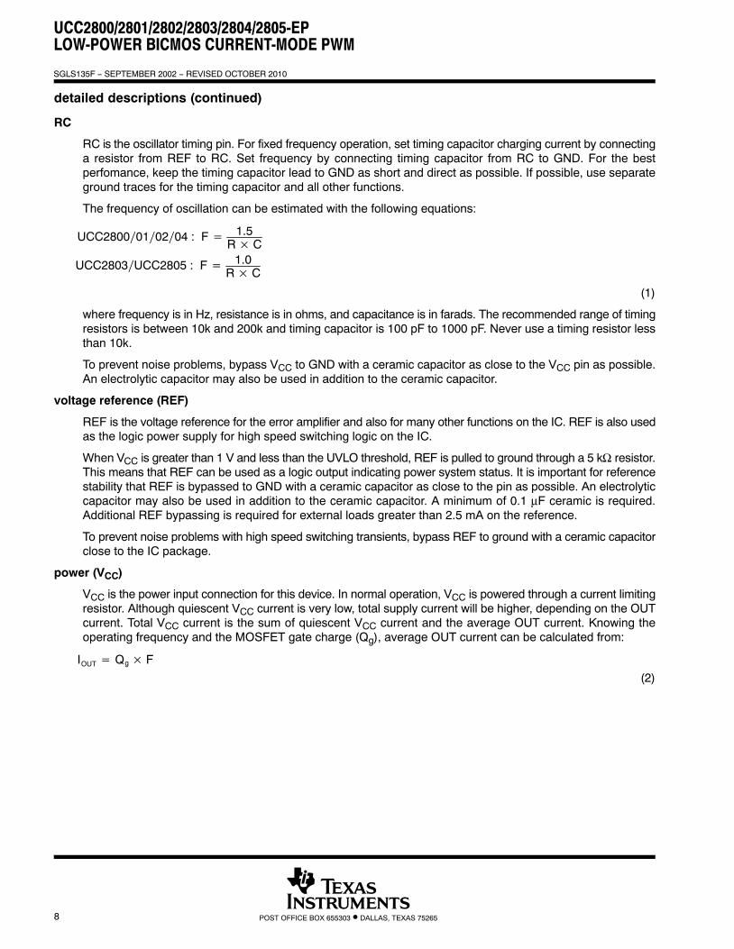
Ordering Information
UCC2 0 Q or M
PACKAGED = Plastic SOIC
PRODUCT OPTION0 through 5
TEMPERATURE RANGE INDICATOR
D
TAPE and REEL INDICATOR
R80 EP
ENHANCED PLASTIC INDICATOR
UCC280XXD−EP Operating Life Derating Chart
1
10
100
1000
100 110 120 130 140 150 160
Yea
rs e
stim
ated
life
Wirebond VoidingFail Mode
Continuous Tj (�C)
NOTES: A. See datasheet for Absolute Maximum and Minimum Recommended Operating ConditionsB. Silicon operating life design Goal is 10 @ 105°C junction temperature (does not include package interconnect life).C. Enhanced plastic product disclaimer applies.

UCC2800/2801/2802/2803/2804/2805-EPLOW-POWER BICMOS CURRENT-MODE PWM�
�
SGLS135F − SEPTEMBER 2002 − REVISED OCTOBER 2010
4 POST OFFICE BOX 655303 • DALLAS, TEXAS 75265
absolute maximum ratings over operating free-air temperature range (unless otherwise noted)†‡
VCC voltage � 12 V. . . . . . . . . . . . . . . . . . . . . . . . . . . . . . . . . . . . . . . . . . . . . . . . . . . . . . . . . . . . . . . . . . . . . . . . . . . . . . VCC current � 30 mA. . . . . . . . . . . . . . . . . . . . . . . . . . . . . . . . . . . . . . . . . . . . . . . . . . . . . . . . . . . . . . . . . . . . . . . . . . . . Output current, IO ±1 A. . . . . . . . . . . . . . . . . . . . . . . . . . . . . . . . . . . . . . . . . . . . . . . . . . . . . . . . . . . . . . . . . . . . . . . . . Output energy (capacitive load) 20 μJ. . . . . . . . . . . . . . . . . . . . . . . . . . . . . . . . . . . . . . . . . . . . . . . . . . . . . . . . . . . . . Analog inputs (FB, CS, RC, COMP) −0.3 V to the lesser of 6.3 V or VCC + 0.3 V. . . . . . . . . . . . . . . . . . . . . . . Power dissipation at TA < +25�C (D package) 0.65 W. . . . . . . . . . . . . . . . . . . . . . . . . . . . . . . . . . . . . . . . . . . . . . . Storage temperature range, Tstg −65�C to 150�C. . . . . . . . . . . . . . . . . . . . . . . . . . . . . . . . . . . . . . . . . . . . . . . . . . . . Lead temperature soldering 1,6 mm (1/16 in) from case for 10s 300�C. . . . . . . . . . . . . . . . . . . . . . . . . . . . . . . .
† Stresses beyond those listed under “absolute maximum ratings” may cause permanent damage to the device. These are stress ratings only, andfunctional operation of the device at these or any other conditions beyond those indicated under “recommended operating conditions” is notimplied. Exposure to absolute-maximum-rated conditions for extended periods may affect device reliability.
‡ Unless otherwise indicated, voltages are reference to ground and currents are positive into and negative out of the specified terminals.
� In normal operation, VCC is powered through a current limiting resistor. Absolute maximum of 12 V applies when VCC is driven from a lowimpedance source such that ICC does not exceed 30 mA (which includes gate drive current requirement).
electrical characteristics, TA = −40�C to 125�C for Q temp and TA= −55�C to 125�C for M temp, VCC= 10 V (see Note 1), RT = 100 kΩ from REF to RC, CT = 330 pF from RC to GND, 0.1 F capacitor fromVCC to GND, 0.1 F capacitor from VREF to GND and TA = TJ (unless otherwise stated)
PARAMETER TEST CONDITIONS
UCC280XQ,UCC280XM UNITPARAMETER TEST CONDITIONS
MIN TYP MAXUNIT
Reference Section
Output voltage T 25�C I 0 2 AUCC2800/01/02/04 4.925 5 5.075
VOutput voltage TJ = 25�C, I = 0.2 mAUCC2803/05 3.94 4 4.06
V
Load regulation voltage I = 0.2 mA to 5 mA 10 30 mV
TJ = 25�C 1.9
Line regulation voltage VCC = 10 V to clamp TJ = −40�C to 125�C and TJ = −55�C to 125�C
2.5mV/V
Total variation voltage See Note 5UCC2800/01/02/04 4.88 5 5.1
VTotal variation voltage See Note 5UCC2803/05 3.9 4 4.08
V
Output noise voltage f = 10 Hz to 10 kHz, See Note 7 TJ = 25�C 130 μV
Long term stability 1000 hours, See Note 7 TA = 125�C 5 mV
Output short-circuit current −5 −35 mA

UCC2800/2801/2802/2803/2804/2805-EPLOW-POWER BICMOS CURRENT-MODE PWM
�
�
SGLS135F − SEPTEMBER 2002 − REVISED OCTOBER 2010
5POST OFFICE BOX 655303 • DALLAS, TEXAS 75265
electrical characteristics, TA = −40�C to 125�C for Q temp and TA= −55�C to 125�C for M temp, VCC= 10 V (see Note 1), RT = 100 kΩ from REF to RC, CT = 330 pF from RC to GND, 0.1 F capacitor fromVCC to GND, 0.1 F capacitor from VREF to GND and TA = TJ (unless otherwise stated)
PARAMETER TEST CONDITIONS
UCC280XQ,UCC280XM UNITPARAMETER TEST CONDITIONS
MIN TYP MAXUNIT
Oscillator Section
Oscillator frequency See Note 2UCC2800/01/02/04 40 46 52
kHzOscillator frequency See Note 2UCC2803/05 26 31 36
kHz
Temperature stability See Note 7 2.5%
Amplitude peak-to-peak 2.25 2.4 2.55 V
Oscillator peak voltage 2.45 V
Error Amplifier Section
Input voltageCOMP = 2.5 V UCC2800/01/02/04 2.44 2.5 2.56
VInput voltageCOMP = 2 V UCC2803/05 1.95 2 2.05
V
Input bias current −1 1 μA
Open loop voltage gain 60 80 db
COMP sink current FB = 2.7 V, COMP = 1.1 V 0.3 3.5 mA
COMP source current FB = 1.8 V, COMP = REF − 1.2 V −0.2 −0.5 −0.8 mA
Gain bandwidth product See Note 7 2 MHz
PWM Section
Maximum duty cycleUCC2800/02/03 97% 99% 100%
Maximum duty cycleUCC2801/04/05 48% 49% 50%
Minimum duty cycle COMP = 0 V 0
Current Sense Section
Gain See Note 3 1.1 1.65 1.8 V/V
Maximum input signal COMP = 5 V, See Note 4 0.9 1 1.1 V
Input bias current −200 200 nA
CS blank time 50 100 150 ns
Overcurrent threshold voltage 1.42 1.55 1.68 V
COMP to CS offset voltage CS = 0 V 0.45 0.9 1.35 V
Output Section (OUT)
IOUT = 20 mA All parts 0.1 0.4
Low level output voltageIOUT = 200 mA All parts 0.35 0.9
VLow-level output voltageIOUT = 50 mA, VCC = 5 V UCC2803/05 0.15 0.4
V
IOUT = 20 mA, VCC = 0 V All parts 0.7 1.2
IOUT = −20 mA All parts 0.15 0.4
High-level output voltage VSAT (VCC − OUT) IOUT = −200 mA All parts 1 1.9 VHigh level output voltage VSAT (VCC OUT)
IOUT = −50 mA, VCC = 5 V UCC2803/05 0.4 0.9
V
Rise time CL = 1 nF 41 70 ns
Fall time CL = 1 nF 44 75 ns

UCC2800/2801/2802/2803/2804/2805-EPLOW-POWER BICMOS CURRENT-MODE PWM�
�
SGLS135F − SEPTEMBER 2002 − REVISED OCTOBER 2010
6 POST OFFICE BOX 655303 • DALLAS, TEXAS 75265
electrical characteristics, TA = −40�C to 125�C for Q temp and TA= −55�C to 125�C for M temp, VCC= 10 V (see Note 1), RT = 100 kΩ from REF to RC, CT = 330 pF from RC to GND, 0.1 F capacitor fromVCC to GND, 0.1 F capacitor from VREF to GND and TA = TJ (unless otherwise stated)
PARAMETER TEST CONDITIONS
UCC280XQ,UCC280XM UNITPARAMETER TEST CONDITIONS
MIN TYP MAXUNIT
Undervoltage Lockout Section
UCC2800 6.6 7.2 7.8
Start threshold See Note 6UCC2801 8.6 9.4 10.2
VStart threshold See Note 6UCC2802/04 11.5 12.5 13.5
V
UCC2803/05 3.7 4.1 4.5
UCC2800 6.3 6.9 7.5
Stop threshold See Note 6UCC2801 6.8 7.4 8
VStop threshold See Note 6UCC2802/04 7.6 8.3 9
V
UCC2803/05 3.2 3.6 4
UCC2800 0.12 0.3 0.48
Start to stop hysteresisUCC2801 1.6 2 2.4
VStart to stop hysteresisUCC2802/04 3.5 4.2 5.1
V
UCC2803/05 0.2 0.5 0.8
Soft Start Section
COMP rise time FB = 1.8 V, Rise from 0.5 V to REF − 1 V 4 10 ms
Overall Section
Start-up current VCC < Start threshold 0.1 0.2 mA
Operating supply current FB = 0 V, CS = 0 V 0.5 1 mA
VCC internal zener voltage ICC = 10 mA, See Note 6 and Note 8 12 13.5 15 V
VCC internal zener voltage minus start threshold voltage See Note 6 UCC2802/04 0.5 1 V
NOTES: 1. Adjust VCC above the start threshold before setting at 10 V.2. Oscillator frequency for the UCC2800, UCC2802, and UCC2803 is the output frequency.
Oscillator frequency for the UCC2801, UCC2804, and UCC2805 is twice the output frequency.
3. Gain is defined by: A =
�VCOMP
�VCS 0 � VCS � 0.8 V4. Parameter measured at trip point of latch with Pin 2 at 0 V5. Total variation includes temperature stability and load regulation.6. Start threshold, stop threshold, and zener shunt thresholds track one another.7. Not production tested8. The device is fully operating in clamp mode as the forcing current is higher than the normal operating supply current.

UCC2800/2801/2802/2803/2804/2805-EPLOW-POWER BICMOS CURRENT-MODE PWM
�
�
SGLS135F − SEPTEMBER 2002 − REVISED OCTOBER 2010
7POST OFFICE BOX 655303 • DALLAS, TEXAS 75265
detailed terminal descriptions
COMP
COMP is the output of the error amplifier and the input of the PWM comparator.
Unlike other devices, the error amplifier in the UCC2800 family is a true, low output-impedance, 2 MHzoperational amplifier. As such, the COMP terminal can both source and sink current. However, the erroramplifier is internally current limited, so that one can command zero duty cycle by externally forcing COMP toGND.
The UCC2800 family features built-in full cycle soft start. Soft start is implemented as a clamp on the maximumCOMP voltage.
CS
CS is the input to the current sense comparators. The UCC2800 family has two different current sensecomparators - the PWM comparator and an overcurrent comparator.
The UCC2800 family contains digital current sense filtering, which disconnects the CS terminal from the currentsense comparator during the 100 ns interval immediately following the rising edge of the OUT pin. This digitalfiltering, also called leading-edge blanking, means that in most applications, no analog filtering (RC filter) isrequired on CS. Compared to an external RC filter technique, the leading-edge blanking provides a smallereffective CS to OUT propagation delay. Note, however, that the minimum non-zero on-time of the OUT signalis directly affected by the leading-edge-blanking and the CS to OUT propagation delay.
The overcurrent comparator is only intended for fault sensing, and exceeding the over-current threshold willcause a soft start cycle.
FB
FB is the inverting input of the error amplifier. For best stability, keep FB lead length as short as possible andFB stray capacitance as small as possible.
ground (GND)
GND is reference ground and power ground for all functions on this part.
OUT
OUT is the output of a high-current power driver capable of driving the gate of a power MOSFET with peakcurrents exceeding 750 mA. OUT is actively held low when VCC is below the UVLO threshold.
The high-current power driver consists of FET output devices, which can switch all of the way to GND and allof the way to VCC. The output stage also provides a low impedance to overshoot and undershoot. This meansthat in many cases, external schottky clamp diodes are not required.
UCC2800/2801/2802/2803/2804/2805-EPLOW-POWER BICMOS CURRENT-MODE PWM�
�
SGLS135F − SEPTEMBER 2002 − REVISED OCTOBER 2010
8 POST OFFICE BOX 655303 • DALLAS, TEXAS 75265
detailed descriptions (continued)
RC
RC is the oscillator timing pin. For fixed frequency operation, set timing capacitor charging current by connectinga resistor from REF to RC. Set frequency by connecting timing capacitor from RC to GND. For the bestperfomance, keep the timing capacitor lead to GND as short and direct as possible. If possible, use separateground traces for the timing capacitor and all other functions.
The frequency of oscillation can be estimated with the following equations:
UCC2800�01�02�04 : F � 1.5R � C
UCC2803�UCC2805 : F � 1.0R � C
where frequency is in Hz, resistance is in ohms, and capacitance is in farads. The recommended range of timingresistors is between 10k and 200k and timing capacitor is 100 pF to 1000 pF. Never use a timing resistor lessthan 10k.
To prevent noise problems, bypass VCC to GND with a ceramic capacitor as close to the VCC pin as possible.An electrolytic capacitor may also be used in addition to the ceramic capacitor.
voltage reference (REF)
REF is the voltage reference for the error amplifier and also for many other functions on the IC. REF is also usedas the logic power supply for high speed switching logic on the IC.
When VCC is greater than 1 V and less than the UVLO threshold, REF is pulled to ground through a 5 kΩ resistor.This means that REF can be used as a logic output indicating power system status. It is important for referencestability that REF is bypassed to GND with a ceramic capacitor as close to the pin as possible. An electrolyticcapacitor may also be used in addition to the ceramic capacitor. A minimum of 0.1 μF ceramic is required.Additional REF bypassing is required for external loads greater than 2.5 mA on the reference.
To prevent noise problems with high speed switching transients, bypass REF to ground with a ceramic capacitorclose to the IC package.
power (VCC)
VCC is the power input connection for this device. In normal operation, VCC is powered through a current limitingresistor. Although quiescent VCC current is very low, total supply current will be higher, depending on the OUTcurrent. Total VCC current is the sum of quiescent VCC current and the average OUT current. Knowing theoperating frequency and the MOSFET gate charge (Qg), average OUT current can be calculated from:
IOUT � Qg � F
(1)
(2)

UCC2800/2801/2802/2803/2804/2805-EPLOW-POWER BICMOS CURRENT-MODE PWM
�
�
SGLS135F − SEPTEMBER 2002 − REVISED OCTOBER 2010
9POST OFFICE BOX 655303 • DALLAS, TEXAS 75265
PARAMETER MEASUREMENT INFORMATION
Figure 1
Oscillator
The UCC3800/1/2/3/4/5 oscillator generates a sawtooth waveformon RC. The rise time is set by the time constant of RT and CT. Thefall time is set by CT and an internal transistor on-resistance ofapproximately 125. During the fall time, the output is off and themaximum duty cycle is reduced below 50% or 100% depending onthe part number. Larger timing capacitors increase the dischargetime and reduce the maximum duty cycle and frequency.
Figure 2
Error AmplifierGain/Phase Response
Figure 3
UCC1803/05 VREF vs VCC; ILOAD = 0.5 mA
Figure 4
UCC1800/01/02/04 Oscillator Frequencyvs RT and CT

UCC2800/2801/2802/2803/2804/2805-EPLOW-POWER BICMOS CURRENT-MODE PWM�
�
SGLS135F − SEPTEMBER 2002 − REVISED OCTOBER 2010
10 POST OFFICE BOX 655303 • DALLAS, TEXAS 75265
PARAMETER MEASUREMENT INFORMATION
Figure 5
UCC1803/05 Oscillator Frequencyvs
RT and CT
Figure 6
UCC1800/02/03 Maximum Duty Cyclevs
Oscillator Frequency
Figure 7
UCC1801/04/05 Maximum Duty Cyclevs
Oscillator Frequency
Figure 8
UCC1800 ICCvs
Oscillator Frequency

UCC2800/2801/2802/2803/2804/2805-EPLOW-POWER BICMOS CURRENT-MODE PWM
�
�
SGLS135F − SEPTEMBER 2002 − REVISED OCTOBER 2010
11POST OFFICE BOX 655303 • DALLAS, TEXAS 75265
PARAMETER MEASUREMENT INFORMATION
Figure 9
UCC1805 ICCvs
Oscillator Frequency
Figure 10
Dead Timevs
CT, RT = 100 k�
Figure 11
COMP to CS Offsetvs
Temperature, CS = 0 V

UCC2800/2801/2802/2803/2804/2805-EPLOW-POWER BICMOS CURRENT-MODE PWM�
�
SGLS135F − SEPTEMBER 2002 − REVISED OCTOBER 2010
12 POST OFFICE BOX 655303 • DALLAS, TEXAS 75265
MECHANICAL DATAD (R-PDSO-G**) PLASTIC SMALL-OUTLINE PACKAGE8 PINS SHOWN
8
0.197(5,00)
A MAX
A MIN(4,80)0.189 0.337
(8,55)
(8,75)0.344
14
0.386(9,80)
(10,00)0.394
16DIM
PINS **
4040047/E 09/01
0.069 (1,75) MAX
Seating Plane
0.004 (0,10)0.010 (0,25)
0.010 (0,25)
0.016 (0,40)0.044 (1,12)
0.244 (6,20)0.228 (5,80)
0.020 (0,51)0.014 (0,35)
1 4
8 5
0.150 (3,81)0.157 (4,00)
0.008 (0,20) NOM
0°− 8°
Gage Plane
A
0.004 (0,10)
0.010 (0,25)0.050 (1,27)
NOTES: A. All linear dimensions are in inches (millimeters).B. This drawing is subject to change without notice.C. Body dimensions do not include mold flash or protrusion, not to exceed 0.006 (0,15).D. Falls within JEDEC MS-012

PACKAGE OPTION ADDENDUM
www.ti.com 10-Jun-2014
Addendum-Page 1
PACKAGING INFORMATION
Orderable Device Status(1)
Package Type PackageDrawing
Pins PackageQty
Eco Plan(2)
Lead/Ball Finish(6)
MSL Peak Temp(3)
Op Temp (°C) Device Marking(4/5)
Samples
UCC2800MDREP ACTIVE SOIC D 8 2500 Green (RoHS& no Sb/Br)
CU NIPDAU Level-1-260C-UNLIM -55 to 125 2800EP
UCC2800QDREP ACTIVE SOIC D 8 2500 Green (RoHS& no Sb/Br)
CU NIPDAU Level-1-260C-UNLIM -40 to 125 C2800DEP
UCC2801MDREP ACTIVE SOIC D 8 2500 Green (RoHS& no Sb/Br)
CU NIPDAU Level-1-260C-UNLIM -55 to 125 2801EP
UCC2801QDREP ACTIVE SOIC D 8 2500 Green (RoHS& no Sb/Br)
CU NIPDAU Level-1-260C-UNLIM -40 to 125 2801EP
UCC2802QDREP ACTIVE SOIC D 8 2500 Green (RoHS& no Sb/Br)
CU NIPDAU Level-1-260C-UNLIM -40 to 125 2802EP
UCC2803MDREP ACTIVE SOIC D 8 2500 Green (RoHS& no Sb/Br)
CU NIPDAU Level-1-260C-UNLIM -55 to 125 2803EP
UCC2803QDREP ACTIVE SOIC D 8 2500 Green (RoHS& no Sb/Br)
CU NIPDAU Level-1-260C-UNLIM -40 to 125 2803EP
UCC2804QDREP ACTIVE SOIC D 8 2500 Green (RoHS& no Sb/Br)
CU NIPDAU Level-1-260C-UNLIM -40 to 125 2804EP
UCC2805QDREP ACTIVE SOIC D 8 2500 Green (RoHS& no Sb/Br)
CU NIPDAU Level-1-260C-UNLIM -40 to 125 2805EP
V62/03624-01XE ACTIVE SOIC D 8 2500 Green (RoHS& no Sb/Br)
CU NIPDAU Level-1-260C-UNLIM -40 to 125 C2800DEP
V62/03624-02XE ACTIVE SOIC D 8 2500 Green (RoHS& no Sb/Br)
CU NIPDAU Level-1-260C-UNLIM -40 to 125 2801EP
V62/03624-03XE ACTIVE SOIC D 8 2500 Green (RoHS& no Sb/Br)
CU NIPDAU Level-1-260C-UNLIM -40 to 125 2802EP
V62/03624-04XE ACTIVE SOIC D 8 2500 Green (RoHS& no Sb/Br)
CU NIPDAU Level-1-260C-UNLIM -40 to 125 2803EP
V62/03624-05XE ACTIVE SOIC D 8 2500 Green (RoHS& no Sb/Br)
CU NIPDAU Level-1-260C-UNLIM -40 to 125 2804EP
V62/03624-06XE ACTIVE SOIC D 8 2500 Green (RoHS& no Sb/Br)
CU NIPDAU Level-1-260C-UNLIM -40 to 125 2805EP
V62/03624-07XE ACTIVE SOIC D 8 2500 Green (RoHS& no Sb/Br)
CU NIPDAU Level-1-260C-UNLIM -55 to 125 2801EP
V62/03624-08XE ACTIVE SOIC D 8 2500 Green (RoHS& no Sb/Br)
CU NIPDAU Level-1-260C-UNLIM -55 to 125 2803EP

PACKAGE OPTION ADDENDUM
www.ti.com 10-Jun-2014
Addendum-Page 2
Orderable Device Status(1)
Package Type PackageDrawing
Pins PackageQty
Eco Plan(2)
Lead/Ball Finish(6)
MSL Peak Temp(3)
Op Temp (°C) Device Marking(4/5)
Samples
V62/03624-09XE ACTIVE SOIC D 8 2500 Green (RoHS& no Sb/Br)
CU NIPDAU Level-1-260C-UNLIM -55 to 125 2800EP
(1) The marketing status values are defined as follows:ACTIVE: Product device recommended for new designs.LIFEBUY: TI has announced that the device will be discontinued, and a lifetime-buy period is in effect.NRND: Not recommended for new designs. Device is in production to support existing customers, but TI does not recommend using this part in a new design.PREVIEW: Device has been announced but is not in production. Samples may or may not be available.OBSOLETE: TI has discontinued the production of the device.
(2) Eco Plan - The planned eco-friendly classification: Pb-Free (RoHS), Pb-Free (RoHS Exempt), or Green (RoHS & no Sb/Br) - please check http://www.ti.com/productcontent for the latest availabilityinformation and additional product content details.TBD: The Pb-Free/Green conversion plan has not been defined.Pb-Free (RoHS): TI's terms "Lead-Free" or "Pb-Free" mean semiconductor products that are compatible with the current RoHS requirements for all 6 substances, including the requirement thatlead not exceed 0.1% by weight in homogeneous materials. Where designed to be soldered at high temperatures, TI Pb-Free products are suitable for use in specified lead-free processes.Pb-Free (RoHS Exempt): This component has a RoHS exemption for either 1) lead-based flip-chip solder bumps used between the die and package, or 2) lead-based die adhesive used betweenthe die and leadframe. The component is otherwise considered Pb-Free (RoHS compatible) as defined above.Green (RoHS & no Sb/Br): TI defines "Green" to mean Pb-Free (RoHS compatible), and free of Bromine (Br) and Antimony (Sb) based flame retardants (Br or Sb do not exceed 0.1% by weightin homogeneous material)
(3) MSL, Peak Temp. - The Moisture Sensitivity Level rating according to the JEDEC industry standard classifications, and peak solder temperature.
(4) There may be additional marking, which relates to the logo, the lot trace code information, or the environmental category on the device.
(5) Multiple Device Markings will be inside parentheses. Only one Device Marking contained in parentheses and separated by a "~" will appear on a device. If a line is indented then it is a continuationof the previous line and the two combined represent the entire Device Marking for that device.
(6) Lead/Ball Finish - Orderable Devices may have multiple material finish options. Finish options are separated by a vertical ruled line. Lead/Ball Finish values may wrap to two lines if the finishvalue exceeds the maximum column width.
Important Information and Disclaimer:The information provided on this page represents TI's knowledge and belief as of the date that it is provided. TI bases its knowledge and belief on informationprovided by third parties, and makes no representation or warranty as to the accuracy of such information. Efforts are underway to better integrate information from third parties. TI has taken andcontinues to take reasonable steps to provide representative and accurate information but may not have conducted destructive testing or chemical analysis on incoming materials and chemicals.TI and TI suppliers consider certain information to be proprietary, and thus CAS numbers and other limited information may not be available for release.
In no event shall TI's liability arising out of such information exceed the total purchase price of the TI part(s) at issue in this document sold by TI to Customer on an annual basis.
OTHER QUALIFIED VERSIONS OF UCC2800-EP, UCC2801-EP, UCC2802-EP, UCC2803-EP, UCC2804-EP, UCC2805-EP :

PACKAGE OPTION ADDENDUM
www.ti.com 10-Jun-2014
Addendum-Page 3
• Catalog: UCC2800, UCC2801, UCC2802, UCC2803, UCC2804, UCC2805
• Automotive: UCC2800-Q1, UCC2801-Q1, UCC2802-Q1, UCC2803-Q1, UCC2804-Q1, UCC2805-Q1
• Military: UCC2802M, UCC2803M
NOTE: Qualified Version Definitions:
• Catalog - TI's standard catalog product
• Automotive - Q100 devices qualified for high-reliability automotive applications targeting zero defects
• Military - QML certified for Military and Defense Applications

TAPE AND REEL INFORMATION
*All dimensions are nominal
Device PackageType
PackageDrawing
Pins SPQ ReelDiameter
(mm)
ReelWidth
W1 (mm)
A0(mm)
B0(mm)
K0(mm)
P1(mm)
W(mm)
Pin1Quadrant
UCC2800MDREP SOIC D 8 2500 330.0 12.4 6.4 5.2 2.1 4.0 12.0 Q1
UCC2800QDREP SOIC D 8 2500 330.0 12.4 6.4 5.2 2.1 4.0 12.0 Q1
UCC2801MDREP SOIC D 8 2500 330.0 12.4 6.4 5.2 2.1 4.0 12.0 Q1
UCC2801QDREP SOIC D 8 2500 330.0 12.4 6.4 5.2 2.1 4.0 12.0 Q1
UCC2802QDREP SOIC D 8 2500 330.0 12.4 6.4 5.2 2.1 4.0 12.0 Q1
UCC2803MDREP SOIC D 8 2500 330.0 12.4 6.4 5.2 2.1 4.0 12.0 Q1
UCC2803QDREP SOIC D 8 2500 330.0 12.4 6.4 5.2 2.1 4.0 12.0 Q1
UCC2804QDREP SOIC D 8 2500 330.0 12.4 6.4 5.2 2.1 4.0 12.0 Q1
UCC2805QDREP SOIC D 8 2500 330.0 12.4 6.4 5.2 2.1 4.0 12.0 Q1
PACKAGE MATERIALS INFORMATION
www.ti.com 15-Sep-2017
Pack Materials-Page 1

*All dimensions are nominal
Device Package Type Package Drawing Pins SPQ Length (mm) Width (mm) Height (mm)
UCC2800MDREP SOIC D 8 2500 367.0 367.0 35.0
UCC2800QDREP SOIC D 8 2500 367.0 367.0 35.0
UCC2801MDREP SOIC D 8 2500 367.0 367.0 35.0
UCC2801QDREP SOIC D 8 2500 367.0 367.0 35.0
UCC2802QDREP SOIC D 8 2500 367.0 367.0 35.0
UCC2803MDREP SOIC D 8 2500 367.0 367.0 35.0
UCC2803QDREP SOIC D 8 2500 367.0 367.0 35.0
UCC2804QDREP SOIC D 8 2500 367.0 367.0 35.0
UCC2805QDREP SOIC D 8 2500 367.0 367.0 35.0
PACKAGE MATERIALS INFORMATION
www.ti.com 15-Sep-2017
Pack Materials-Page 2

IMPORTANT NOTICE
Texas Instruments Incorporated (TI) reserves the right to make corrections, enhancements, improvements and other changes to itssemiconductor products and services per JESD46, latest issue, and to discontinue any product or service per JESD48, latest issue. Buyersshould obtain the latest relevant information before placing orders and should verify that such information is current and complete.TI’s published terms of sale for semiconductor products (http://www.ti.com/sc/docs/stdterms.htm) apply to the sale of packaged integratedcircuit products that TI has qualified and released to market. Additional terms may apply to the use or sale of other types of TI products andservices.Reproduction of significant portions of TI information in TI data sheets is permissible only if reproduction is without alteration and isaccompanied by all associated warranties, conditions, limitations, and notices. TI is not responsible or liable for such reproduceddocumentation. Information of third parties may be subject to additional restrictions. Resale of TI products or services with statementsdifferent from or beyond the parameters stated by TI for that product or service voids all express and any implied warranties for theassociated TI product or service and is an unfair and deceptive business practice. TI is not responsible or liable for any such statements.Buyers and others who are developing systems that incorporate TI products (collectively, “Designers”) understand and agree that Designersremain responsible for using their independent analysis, evaluation and judgment in designing their applications and that Designers havefull and exclusive responsibility to assure the safety of Designers' applications and compliance of their applications (and of all TI productsused in or for Designers’ applications) with all applicable regulations, laws and other applicable requirements. Designer represents that, withrespect to their applications, Designer has all the necessary expertise to create and implement safeguards that (1) anticipate dangerousconsequences of failures, (2) monitor failures and their consequences, and (3) lessen the likelihood of failures that might cause harm andtake appropriate actions. Designer agrees that prior to using or distributing any applications that include TI products, Designer willthoroughly test such applications and the functionality of such TI products as used in such applications.TI’s provision of technical, application or other design advice, quality characterization, reliability data or other services or information,including, but not limited to, reference designs and materials relating to evaluation modules, (collectively, “TI Resources”) are intended toassist designers who are developing applications that incorporate TI products; by downloading, accessing or using TI Resources in anyway, Designer (individually or, if Designer is acting on behalf of a company, Designer’s company) agrees to use any particular TI Resourcesolely for this purpose and subject to the terms of this Notice.TI’s provision of TI Resources does not expand or otherwise alter TI’s applicable published warranties or warranty disclaimers for TIproducts, and no additional obligations or liabilities arise from TI providing such TI Resources. TI reserves the right to make corrections,enhancements, improvements and other changes to its TI Resources. TI has not conducted any testing other than that specificallydescribed in the published documentation for a particular TI Resource.Designer is authorized to use, copy and modify any individual TI Resource only in connection with the development of applications thatinclude the TI product(s) identified in such TI Resource. NO OTHER LICENSE, EXPRESS OR IMPLIED, BY ESTOPPEL OR OTHERWISETO ANY OTHER TI INTELLECTUAL PROPERTY RIGHT, AND NO LICENSE TO ANY TECHNOLOGY OR INTELLECTUAL PROPERTYRIGHT OF TI OR ANY THIRD PARTY IS GRANTED HEREIN, including but not limited to any patent right, copyright, mask work right, orother intellectual property right relating to any combination, machine, or process in which TI products or services are used. Informationregarding or referencing third-party products or services does not constitute a license to use such products or services, or a warranty orendorsement thereof. Use of TI Resources may require a license from a third party under the patents or other intellectual property of thethird party, or a license from TI under the patents or other intellectual property of TI.TI RESOURCES ARE PROVIDED “AS IS” AND WITH ALL FAULTS. TI DISCLAIMS ALL OTHER WARRANTIES ORREPRESENTATIONS, EXPRESS OR IMPLIED, REGARDING RESOURCES OR USE THEREOF, INCLUDING BUT NOT LIMITED TOACCURACY OR COMPLETENESS, TITLE, ANY EPIDEMIC FAILURE WARRANTY AND ANY IMPLIED WARRANTIES OFMERCHANTABILITY, FITNESS FOR A PARTICULAR PURPOSE, AND NON-INFRINGEMENT OF ANY THIRD PARTY INTELLECTUALPROPERTY RIGHTS. TI SHALL NOT BE LIABLE FOR AND SHALL NOT DEFEND OR INDEMNIFY DESIGNER AGAINST ANY CLAIM,INCLUDING BUT NOT LIMITED TO ANY INFRINGEMENT CLAIM THAT RELATES TO OR IS BASED ON ANY COMBINATION OFPRODUCTS EVEN IF DESCRIBED IN TI RESOURCES OR OTHERWISE. IN NO EVENT SHALL TI BE LIABLE FOR ANY ACTUAL,DIRECT, SPECIAL, COLLATERAL, INDIRECT, PUNITIVE, INCIDENTAL, CONSEQUENTIAL OR EXEMPLARY DAMAGES INCONNECTION WITH OR ARISING OUT OF TI RESOURCES OR USE THEREOF, AND REGARDLESS OF WHETHER TI HAS BEENADVISED OF THE POSSIBILITY OF SUCH DAMAGES.Unless TI has explicitly designated an individual product as meeting the requirements of a particular industry standard (e.g., ISO/TS 16949and ISO 26262), TI is not responsible for any failure to meet such industry standard requirements.Where TI specifically promotes products as facilitating functional safety or as compliant with industry functional safety standards, suchproducts are intended to help enable customers to design and create their own applications that meet applicable functional safety standardsand requirements. Using products in an application does not by itself establish any safety features in the application. Designers mustensure compliance with safety-related requirements and standards applicable to their applications. Designer may not use any TI products inlife-critical medical equipment unless authorized officers of the parties have executed a special contract specifically governing such use.Life-critical medical equipment is medical equipment where failure of such equipment would cause serious bodily injury or death (e.g., lifesupport, pacemakers, defibrillators, heart pumps, neurostimulators, and implantables). Such equipment includes, without limitation, allmedical devices identified by the U.S. Food and Drug Administration as Class III devices and equivalent classifications outside the U.S.TI may expressly designate certain products as completing a particular qualification (e.g., Q100, Military Grade, or Enhanced Product).Designers agree that it has the necessary expertise to select the product with the appropriate qualification designation for their applicationsand that proper product selection is at Designers’ own risk. Designers are solely responsible for compliance with all legal and regulatoryrequirements in connection with such selection.Designer will fully indemnify TI and its representatives against any damages, costs, losses, and/or liabilities arising out of Designer’s non-compliance with the terms and provisions of this Notice.
Mailing Address: Texas Instruments, Post Office Box 655303, Dallas, Texas 75265Copyright © 2017, Texas Instruments Incorporated

Mouser Electronics
Authorized Distributor
Click to View Pricing, Inventory, Delivery & Lifecycle Information: Texas Instruments:
UCC2804QDREP V62/03624-05XE