Embed Size (px)
Citation preview

Web Site: www.axman.com
Support: [email protected]
TWR-DEV-PERIPH Peripheral Module for Freescale TOWER System
Hardware User Guide
D O C - 0 5 8 5 - 0 1 0 , R E V D M A Y 2 8 , 2 0 1 4
T W R - D E V - P E R I P H
2
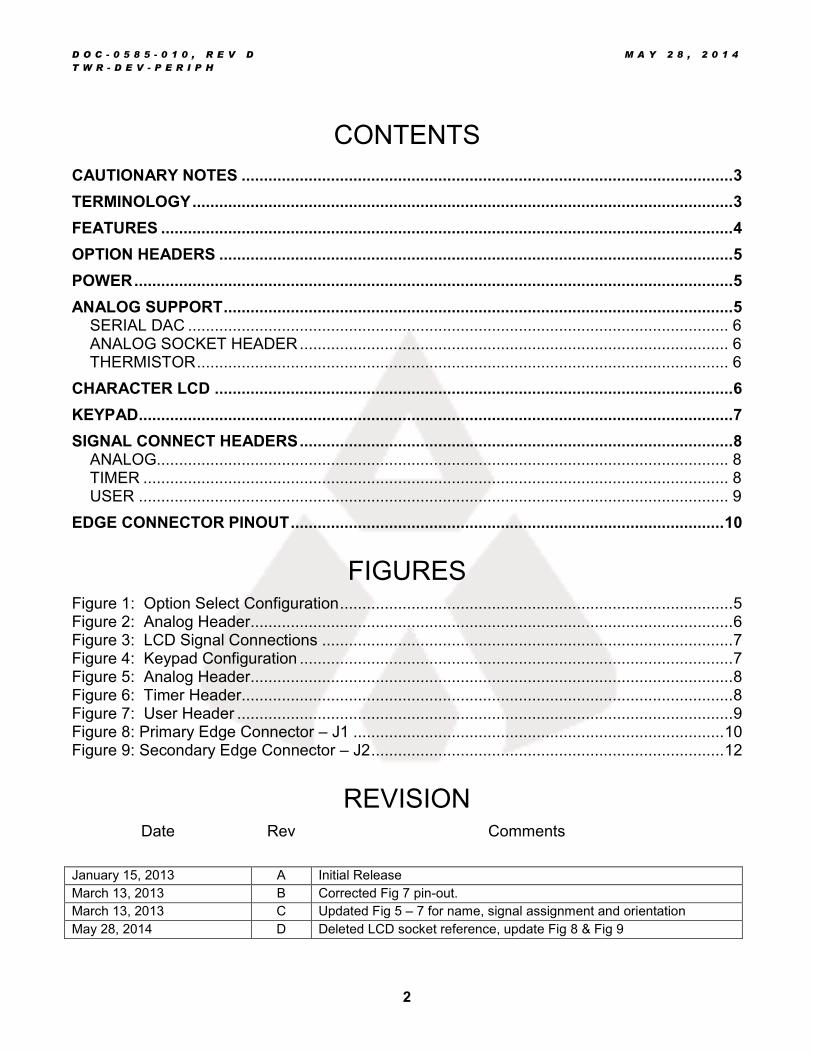
CONTENTS
CAUTIONARY NOTES .............................................................................................................. 3
TERMINOLOGY ......................................................................................................................... 3
FEATURES ................................................................................................................................ 4
OPTION HEADERS ................................................................................................................... 5
POWER ...................................................................................................................................... 5
ANALOG SUPPORT .................................................................................................................. 5
SERIAL DAC ......................................................................................................................... 6
ANALOG SOCKET HEADER ................................................................................................ 6
THERMISTOR ....................................................................................................................... 6
CHARACTER LCD .................................................................................................................... 6
KEYPAD ..................................................................................................................................... 7
SIGNAL CONNECT HEADERS ................................................................................................. 8
ANALOG................................................................................................................................ 8 TIMER ................................................................................................................................... 8 USER .................................................................................................................................... 9
EDGE CONNECTOR PINOUT ................................................................................................. 10
FIGURES Figure 1: Option Select Configuration ........................................................................................ 5
Figure 2: Analog Header............................................................................................................ 6 Figure 3: LCD Signal Connections ............................................................................................ 7 Figure 4: Keypad Configuration ................................................................................................. 7
Figure 5: Analog Header............................................................................................................ 8 Figure 6: Timer Header.............................................................................................................. 8 Figure 7: User Header ............................................................................................................... 9 Figure 8: Primary Edge Connector – J1 ................................................................................... 10
Figure 9: Secondary Edge Connector – J2 ............................................................................... 12
REVISION Date Rev Comments
January 15, 2013 A Initial Release
March 13, 2013 B Corrected Fig 7 pin-out.
March 13, 2013 C Updated Fig 5 – 7 for name, signal assignment and orientation
May 28, 2014 D Deleted LCD socket reference, update Fig 8 & Fig 9

D O C - 0 5 8 5 - 0 1 0 , R E V D M A Y 2 8 , 2 0 1 4
T W R - D E V - P E R I P H
3
CAUTIONARY NOTES
1) Electrostatic Discharge (ESD) prevention measures should be used when handling this product. ESD damage is not a warranty repair item.
2) Axiom Manufacturing does not assume any liability arising out of the application or use of any product or circuit described herein; neither does it convey any license under patent rights or the rights of others.
3) EMC Information on the TWR-S12G128 board:
a) This product has not been tested for compliance to CE and FCC requirements. The user has responsibility to ensure this product neither adversely affects nearby electronic equipment nor suffers adverse effects from nearby electronic equipment.
b) This product is designed and intended for use as a development platform for hardware or software in an educational or professional laboratory.
c) In a domestic environment, this product may cause radio interference in which case the user may be required to take adequate prevention measures.
d) Attaching additional wiring to this product or modifying the products operation from the factory default as shipped may affect its performance and cause interference with nearby electronic equipment. If such interference is detected, suitable mitigating measures should be taken.
TERMINOLOGY
This development module utilizes option select jumpers to configure default board operation. Terminology for application of the option jumpers is as follows:
Jumper – a plastic shunt that connects 2 terminals electrically
Jumper on, in, or installed = jumper is a plastic shunt that fits across 2 pins and the shunt is installed so that the 2 pins are connected with the shunt.
Jumper off, out, or idle = jumper or shunt is installed so that only 1 pin holds the shunt, no 2 pins are connected, or jumper is removed. It is recommended that the jumpers be placed idle by installing on 1 pin so they will not be lost.
Signal names followed by an asterisk (*) denote active-low signals.
D O C - 0 5 8 5 - 0 1 0 , R E V D M A Y 2 8 , 2 0 1 4
T W R - D E V - P E R I P H
4
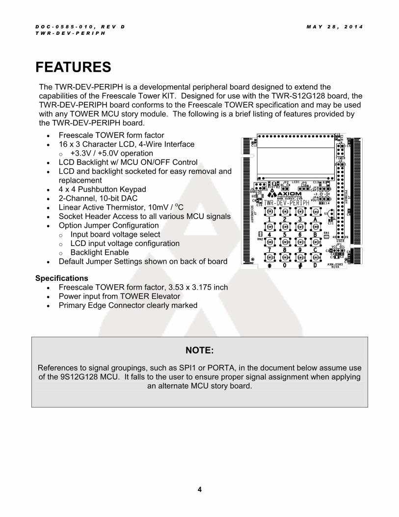
FEATURES
The TWR-DEV-PERIPH is a developmental peripheral board designed to extend the capabilities of the Freescale Tower KIT. Designed for use with the TWR-S12G128 board, the TWR-DEV-PERIPH board conforms to the Freescale TOWER specification and may be used with any TOWER MCU story module. The following is a brief listing of features provided by the TWR-DEV-PERIPH board.
Freescale TOWER form factor 16 x 3 Character LCD, 4-Wire Interface
o +3.3V / +5.0V operation LCD Backlight w/ MCU ON/OFF Control LCD and backlight socketed for easy removal and
replacement 4 x 4 Pushbutton Keypad 2-Channel, 10-bit DAC Linear Active Thermistor, 10mV / oC Socket Header Access to all various MCU signals Option Jumper Configuration
o Input board voltage select o LCD input voltage configuration o Backlight Enable
Default Jumper Settings shown on back of board
Specifications Freescale TOWER form factor, 3.53 x 3.175 inch Power input from TOWER Elevator Primary Edge Connector clearly marked
NOTE:
References to signal groupings, such as SPI1 or PORTA, in the document below assume use of the 9S12G128 MCU. It falls to the user to ensure proper signal assignment when applying
an alternate MCU story board.
D O C - 0 5 8 5 - 0 1 0 , R E V D M A Y 2 8 , 2 0 1 4
T W R - D E V - P E R I P H
5
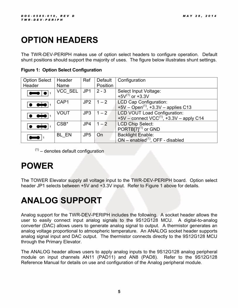
OPTION HEADERS
The TWR-DEV-PERIPH makes use of option select headers to configure operation. Default shunt positions should support the majority of uses. The figure below illustrates shunt settings.
Figure 1: Option Select Configuration
Option Select Header
Header Name
Ref Default Position
Configuration
VCC_SEL JP1 2 - 3 Select Input Voltage: +5V(1) or +3.3V
CAP1 JP2 1 – 2 LCD Cap Configuration: +5V – Open(1), +3.3V – applies C13
VOUT JP3 1 – 2 LCD VOUT Load Configuration: +5V – connect VCC(1), +3.3V – apply C14
CSB* JP4 1 – 2 LCD Chip Select: PORTB[7](1) or GND
BL_EN JP5 On Backlight Enable: ON – enabled(1), OFF - disabled
(1) – denotes default configuration
POWER
The TOWER Elevator supply all voltage input to the TWR-DEV-PERIPH board. Option select header JP1 selects between +5V and +3.3V input. Refer to Figure 1 above for details.
ANALOG SUPPORT
Analog support for the TWR-DEV-PERIPH includes the following. A socket header allows the user to easily connect input analog signals to the 9S12G128 MCU. A digital-to-analog converter (DAC) allows users to generate analog signal to output. A thermistor generates an analog voltage proportional to atmospheric temperature. An ANALOG socket header supports analog signal input and DAC output. The thermistor connects directly to the 9S12G128 MCU through the Primary Elevator.
The ANALOG header allows users to apply analog inputs to the 9S12G128 analog peripheral module on input channels AN11 (PAD11) and AN8 (PAD8). Refer to the 9S12G128 Reference Manual for details on use and configuration of the Analog peripheral module.
1
1
1
1
1
D O C - 0 5 8 5 - 0 1 0 , R E V D M A Y 2 8 , 2 0 1 4
T W R - D E V - P E R I P H
6
Serial DAC
A dual, 10-bit digital-to-analog converter (DAC) allows users to generate output analog signals. The board applies the LTC1661CMS8#PBF located at U2. The 9S12G128 controls the DAC using serial peripheral interface channel 1 (SPI1).
Refer to the LTC1661CMS8#PBF data sheet for complete details on use and configuration. The datasheet may be downloaded from the Axiom Support website.
Analog Socket Header
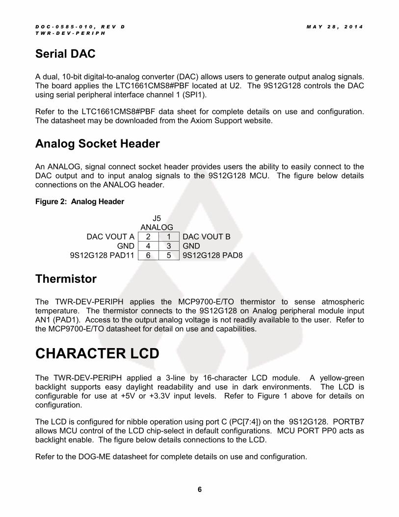
An ANALOG, signal connect socket header provides users the ability to easily connect to the DAC output and to input analog signals to the 9S12G128 MCU. The figure below details connections on the ANALOG header.
Figure 2: Analog Header
J5 ANALOG
DAC VOUT A 2 1 DAC VOUT B
GND 4 3 GND
9S12G128 PAD11 6 5 9S12G128 PAD8
Thermistor
The TWR-DEV-PERIPH applies the MCP9700-E/TO thermistor to sense atmospheric temperature. The thermistor connects to the 9S12G128 on Analog peripheral module input AN1 (PAD1). Access to the output analog voltage is not readily available to the user. Refer to the MCP9700-E/TO datasheet for detail on use and capabilities.
CHARACTER LCD
The TWR-DEV-PERIPH applied a 3-line by 16-character LCD module. A yellow-green backlight supports easy daylight readability and use in dark environments. The LCD is configurable for use at +5V or +3.3V input levels. Refer to Figure 1 above for details on configuration.
The LCD is configured for nibble operation using port C (PC[7:4]) on the 9S12G128. PORTB7 allows MCU control of the LCD chip-select in default configurations. MCU PORT PP0 acts as backlight enable. The figure below details connections to the LCD.
Refer to the DOG-ME datasheet for complete details on use and configuration.
D O C - 0 5 8 5 - 0 1 0 , R E V D M A Y 2 8 , 2 0 1 4
T W R - D E V - P E R I P H
7
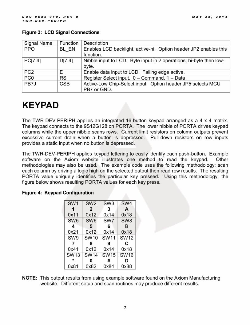
Figure 3: LCD Signal Connections
Signal Name Function Description
PPO BL_EN Enables LCD backlight, active-hi. Option header JP2 enables this function.
PC[7:4] D[7:4] Nibble input to LCD. Byte input in 2 operations; hi-byte then low-byte.
PC2 E Enable data input to LCD. Falling edge active.
PC0 RS Register Select input. 0 – Command, 1 – Data
PB7J CSB Active-Low Chip-Select input. Option header JP5 selects MCU PB7 or GND.
KEYPAD
The TWR-DEV-PERIPH applies an integrated 16-button keypad arranged as a 4 x 4 matrix. The keypad connects to the 9S12G128 on PORTA. The lower nibble of PORTA drives keypad columns while the upper nibble scans rows. Current limit resistors on column outputs prevent excessive current drain when a button is depressed. Pull-down resistors on row inputs provides a static input when no button is depressed.
The TWR-DEV-PERIPH applies keypad lettering to easily identify each push-button. Example software on the Axiom website illustrates one method to read the keypad. Other methodologies may also be used. The example code uses the following methodology; scan each column by driving a logic high on the selected output then read row results. The resulting PORTA value uniquely identifies the particular key pressed. Using this methodology, the figure below shows resulting PORTA values for each key press.
Figure 4: Keypad Configuration
SW1 1
0x11
SW2 2
0x12
SW3 3
0x14
SW4 A
0x18
SW5 4
0x21
SW6 5
0x12
SW7 6
0x14
SW8 B 0x18
SW9 7
0x41
SW10 8
0x12
SW11 9
0x14
SW12 C
0x18
SW13 *
0x81
SW14 0
0x82
SW15 #
0x84
SW16 D
0x88
NOTE: This output results from using example software found on the Axiom Manufacturing
website. Different setup and scan routines may produce different results.
D O C - 0 5 8 5 - 0 1 0 , R E V D M A Y 2 8 , 2 0 1 4
T W R - D E V - P E R I P H
8
In the table above, the top line denotes the pushbutton switch (PBSW) name as seen on the schematic. The 2nd line denotes the silkscreen switch label applied to the board. Users will find this label below the referenced switch. The 3rd line indicates the resultant PORTA value with the indicated switch pressed. As noted above, these results depend on use of example software from the Axiom website. Use of different scan routines may produce different results.
SIGNAL CONNECT HEADERS
The TWR-DEV-PERIPH supports user connection to target MCU signals by means of socket headers. These signal connect headers support 22ga – 26ga solid wire connections. Use of stranded wire is not recommended. Refer to the figures below for pinout of each socket header.
Analog
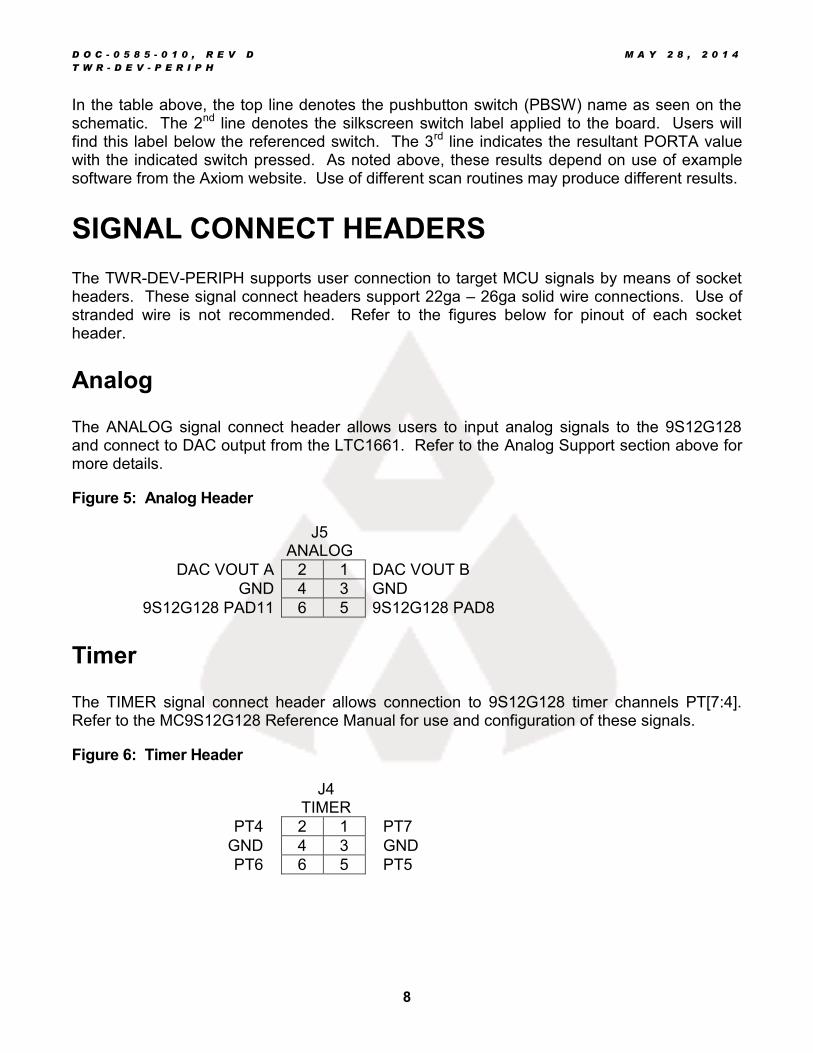
The ANALOG signal connect header allows users to input analog signals to the 9S12G128 and connect to DAC output from the LTC1661. Refer to the Analog Support section above for more details.
Figure 5: Analog Header
J5 ANALOG
DAC VOUT A 2 1 DAC VOUT B
GND 4 3 GND
9S12G128 PAD11 6 5 9S12G128 PAD8
Timer
The TIMER signal connect header allows connection to 9S12G128 timer channels PT[7:4]. Refer to the MC9S12G128 Reference Manual for use and configuration of these signals.
Figure 6: Timer Header
J4 TIMER
PT4 2 1 PT7
GND 4 3 GND
PT6 6 5 PT5
D O C - 0 5 8 5 - 0 1 0 , R E V D M A Y 2 8 , 2 0 1 4
T W R - D E V - P E R I P H
9
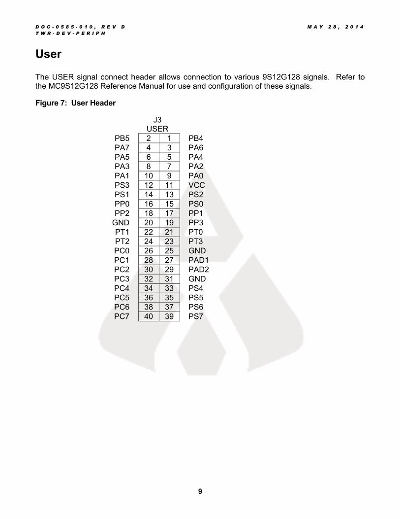
User
The USER signal connect header allows connection to various 9S12G128 signals. Refer to the MC9S12G128 Reference Manual for use and configuration of these signals.
Figure 7: User Header
J3 USER
PB5 2 1 PB4
PA7 4 3 PA6
PA5 6 5 PA4
PA3 8 7 PA2
PA1 10 9 PA0
PS3 12 11 VCC
PS1 14 13 PS2
PP0 16 15 PS0
PP2 18 17 PP1
GND 20 19 PP3
PT1 22 21 PT0
PT2 24 23 PT3
PC0 26 25 GND
PC1 28 27 PAD1
PC2 30 29 PAD2
PC3 32 31 GND
PC4 34 33 PS4
PC5 36 35 PS5
PC6 38 37 PS6
PC7 40 39 PS7
D O C - 0 5 8 5 - 0 1 0 , R E V D M A Y 2 8 , 2 0 1 4
T W R - D E V - P E R I P H
10
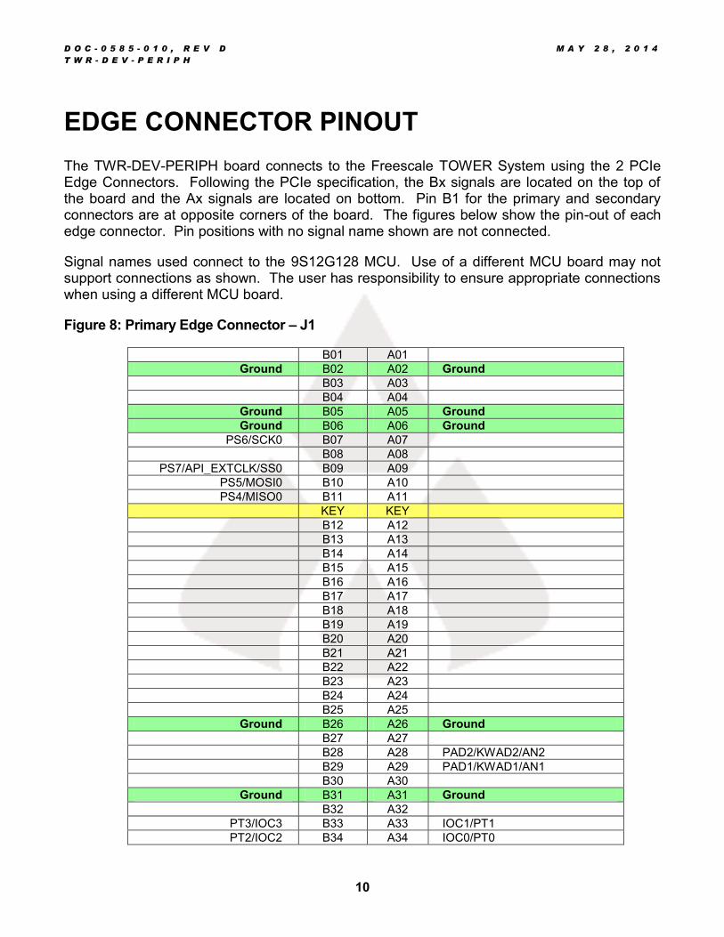
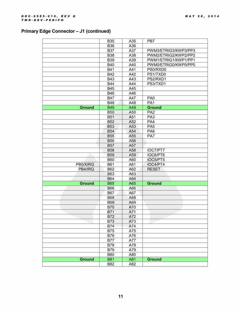
EDGE CONNECTOR PINOUT
The TWR-DEV-PERIPH board connects to the Freescale TOWER System using the 2 PCIe Edge Connectors. Following the PCIe specification, the Bx signals are located on the top of the board and the Ax signals are located on bottom. Pin B1 for the primary and secondary connectors are at opposite corners of the board. The figures below show the pin-out of each edge connector. Pin positions with no signal name shown are not connected.
Signal names used connect to the 9S12G128 MCU. Use of a different MCU board may not support connections as shown. The user has responsibility to ensure appropriate connections when using a different MCU board.
Figure 8: Primary Edge Connector – J1
B01 A01
Ground B02 A02 Ground
B03 A03
B04 A04
Ground B05 A05 Ground
Ground B06 A06 Ground
PS6/SCK0 B07 A07
B08 A08
PS7/API_EXTCLK/SS0 B09 A09 PS5/MOSI0 B10 A10 PS4/MISO0 B11 A11 KEY KEY
B12 A12
B13 A13
B14 A14
B15 A15
B16 A16
B17 A17
B18 A18
B19 A19
B20 A20
B21 A21
B22 A22
B23 A23
B24 A24
B25 A25
Ground B26 A26 Ground
B27 A27
B28 A28 PAD2/KWAD2/AN2
B29 A29 PAD1/KWAD1/AN1
B30 A30
Ground B31 A31 Ground
B32 A32
PT3/IOC3 B33 A33 IOC1/PT1
PT2/IOC2 B34 A34 IOC0/PT0
D O C - 0 5 8 5 - 0 1 0 , R E V D M A Y 2 8 , 2 0 1 4
T W R - D E V - P E R I P H
11
Primary Edge Connector – J1 (continued)
B35 A35 PB7
B36 A36
B37 A37 PWM3/ETRIG3/KWP3/PP3
B38 A38 PWM2/ETRIG2/KWP2/PP2
B39 A39 PWM1/ETRIG1/KWP1/PP1
B40 A40 PWM0/ETRIG0/KWP0/PP0
B41 A41 PS0/RXD0
B42 A42 PS1/TXD0
B43 A43 PS2/RXD1
B44 A44 PS3/TXD1
B45 A45
B46 A46
B47 A47 PA0
B48 A48 PA1
Ground B49 A49 Ground
B50 A50 PA2
B51 A51 PA3
B52 A52 PA4
B53 A53 PA5
B54 A54 PA6
B55 A55 PA7
B56 A56
B57 A57
B58 A58 IOC7/PT7
B59 A59 IOC6/PT6
B60 A60 IOC5/PT5
PB5/XIRQ B61 A61 IOC4/PT4
PB4/IRQ B62 A62 RESET
B63 A63
B64 A64 Ground B65 A65 Ground
B66 A66
B67 A67
B68 A68
B69 A69
B70 A70
B71 A71
B72 A72
B73 A73
B74 A74
B75 A75
B76 A76
B77 A77
B78 A78
B79 A79
B80 A80
Ground B81 A81 Ground
B82 A82

D O C - 0 5 8 5 - 0 1 0 , R E V D M A Y 2 8 , 2 0 1 4
T W R - D E V - P E R I P H
12
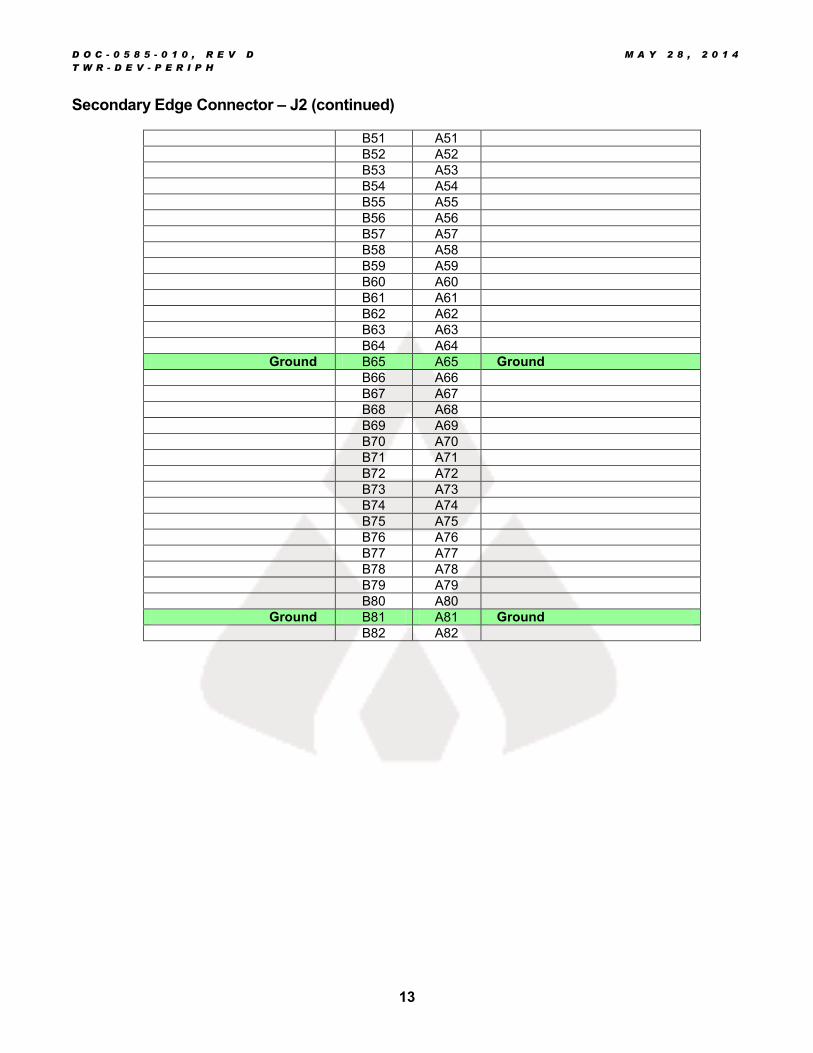
Figure 9: Secondary Edge Connector – J2
B01 A01
Ground B02 A02 Ground
B03 A03
B04 A04
Ground B05 A05 Ground
Ground B06 A06 Ground
SCK1/KWJ2/PJ2 B07 A07
B08 A08
SS1/KWJ3/PJ3 B09 A09 PC0
MOSI1/KWJ1/PJ1 B10 A10
B11 A11
KEY KEY
B12 A12
B13 A13
B14 A14
B15 A15
PC1 B16 A16
PC2 B17 A17 PC3
PC4 B18 A18 PC5
B19 A19
B20 A20
B21 A21
B22 A22
B23 A23
B24 A24
B25 A25
Ground B26 A26 Ground
B27 A27 PAD11/KWAD11/AN11
B28 A28
B29 A29
B30 A30 PAD8/KWAD8/AN8
Ground B31 A31 Ground
B32 A32
B33 A33
B34 A34
PC6 B35 A35 PC7
B36 A36
B37 A37
B38 A38
B39 A39
B40 A40
B41 A41 B42 A42
B43 A43
B44 A44
B45 A45
B46 A46
B47 A47
B48 A48
Ground B49 A49 Ground
B50 A50
D O C - 0 5 8 5 - 0 1 0 , R E V D M A Y 2 8 , 2 0 1 4
T W R - D E V - P E R I P H
13
Secondary Edge Connector – J2 (continued)
B51 A51
B52 A52
B53 A53
B54 A54
B55 A55
B56 A56
B57 A57
B58 A58
B59 A59
B60 A60
B61 A61
B62 A62
B63 A63
B64 A64
Ground B65 A65 Ground
B66 A66
B67 A67
B68 A68
B69 A69
B70 A70
B71 A71
B72 A72
B73 A73
B74 A74
B75 A75
B76 A76
B77 A77
B78 A78
B79 A79
B80 A80
Ground B81 A81 Ground
B82 A82