Embed Size (px)
Citation preview

1
TSEA44: Computer hardware – a system on a chip
Andreas Ehliar, Andreas Karlsson, Kent Palmqvisthttp://www.da.isy.liu.se/courses/tsea44/
”dafk””tsea21””tsea02”

2
What is the course about? How to build a complete embedded computer using an
FPGA and a few other components. Why? Only one chip The computer can easily be tailored to your needs.
Special instructions Accelerators DMA transfer
The computer can be simulated A logic analyzer can be added in the FPGA
Add performance counters It’s fun!

Prerequisites
3
You will definitely need a thorough understanding of
* Digital logic design. You will design both a data path and a control unit for an accelerator.
* Binary arithmetic. Signed/unsigned numbers.
* VHDL or Verilog. SystemVerilog (SV) is the language used in the course.
* Computer Architecture. It is extremely important to understand how a CPU executes code. You will also design part of a DMA-controller. Bus cycles are central.
* Asm and C programming. Most of the programming is done in C, with a few cases of inline asm.

4
Course organisation Lab course: 4 mini projects
6 groups * 3 students in the lab Lab 0: learn enough Verilog, 4
hours
Lectures: 8*2 hours
Examination 6CPs: 3 written reports/group oral individual questions

5
The lab course is based on an application
2004 - trackingThe application is inspired from a robot football web page: http://www.tech.plym.ac.uk/robofoot/
camera
our FPGA computer
1 robotB/W
VGA

6
The lab course is based on an application 2005-12 – JPEG compression
CPUbitfield instr.
• 2-D DCT acc• Quantization• DMA
I/O camera
eth
Take 2-D DCT on 8x8-blocks Quantize = Divide and set small values to zero RLE + Huffman code
Acc.
Mem
testbild.raw -> testbild.jpg

7
Lab info 0) Build a UART in Verilog
1) Interface your UART Test performance counters Test a SW-DCT2 application
2+3) Build a HW accelerator for 2-D DCT and add a DMA controller
4) Design your own instruction to handle bit fields
FPGA CPU
bit instr.
2-D DCTQuantization
DMA
UART
eth
mem

8
Lab nr
Lab task Examination
0 Build a UART in Verilog Demonstration
1Interfacing to theWishbone bus
DemonstrationWritten report
2+3Design a JPEG accelerator + DMA
DemonstrationWritten report
4 Custom InstructionDemonstrationWritten report
•Lab 0 should be done on an individual basis•Your group shall send in 3 written lab reports in PDF format (via Urkund).
Demonstration = presentation of working design. We ask individual questions!
Written report = a readable short report typically consisting of - Introduction - Design, where you explain with text and diagrams how your design works - Results, that you have measured - Conclusions - Appendix : All Verilog and C code with comments!

9
Competition – fastest JPEG compression
wunderb.jpg320 x 240
Wunderbart-tårtan
• An unaccelerated JPEG compression (using jpegfiles) takes roughly 13,0 Mcycles (25 Mhz).
• Our record: ~100000 cycles (everything in hardware at this point).• Goal: Highest frame rate. Exception: At over 25 FPS, the smallest
implementation wins.

10
Communication &Memory Module
Main Board

11
Our ”soft” computer

12

13
(System)Verilog!
The course uses SystemVerilog! SystemVerilog is easy to learn if you
know VHDL/C Our soft computer (80 % downloaded
from OpenCores) is written in Verilog It is possible to use both languages in
a design You need to understand parts of the
computer

14
SystemVerilog vs VHDLan edge-triggered D-flip/flop
C-like syntax
module dff( input clk, d, output reg q);
always_ff @(posedge clk)q <= d;
endmodule
Ada-like syntax
entity dff isport (clk,d : in std_logic; q: out std_logic);end dff;
architecture firsttry of dff is beginprocess (clk) begin if rising_edge(clk) then q <= d; end if;end process;end firsttry;d q
clk

15
SystemVerilog vs VHDLlet’s use our D-flip/flop, instantiation
d qac
b
// instantiation
wire a,b,c,grr;...
dff ff1(.clk(c),.d(a), .q(grr));
dff ff2(.clk(c), .d(grrr), .q(b));
d q
Watch out! Verilog allows implicit declarations (but this can be disabled)
ff2 ff2grr

16
You get a lab skeleton!• dafk_tb.sv . Testbench.– dafk_top.sv . To be synthesized in the FPGA.
. eth_top.sv. Ethernet controller.
. pkmc_top.sv. Memory controller.
. or1200_top.sv. The OR1200 CPU.
. parport.sv. Simple parallel port.
. romram.sv . The boot code resides here.
. uart_top.sv . UART 16550.
. dvga_top.sv . VGA controller.
. wb_top.sv . The wishbone bus.– eth_phy.v . Simulation model for the PHY chip.– flash.v Simulation model.– sdram.v Simulation model.– sram.v . Simulation model.

17
The Wishbone busA multi-master bus • Signals: adress (32), data_out(32), data_in(32), control• Two data buses and muxes are used instead of tristate
M0
M1
S0
S1
S2

18
”The environment”
eth
Home directory
Server
130.236.x.y
LinuxXilinx ISEModelSimgtktermTFTPmake simmake dafkor32-uclinux-gccprecision
pc 192.168.0.101
FPGAmonitor(rs232)uClinux * tftp * jpegtest
192.168.0.231
rs232
ProgrammingCable IV
We prefer linux (centos) but you can also use windows Compile uClinux only on linux
130.236.z.w

19
Software under linux
C-compiler (GNU tool chain) or32-uclinux-gcc
Software simulator or32-uclinux-sim
a very simple boot monitor (24 kB ROM + 8 kB RAMinside FPGA) dct_sw, dma_dct_sw,jpegtest
Clinux boots from flash jpegtest
board
host

20
booting uClinux
uClinux/OR32Flat model support (C) 1998,1999 Kenneth Albanowski, D. Jeff DionneCalibrating delay loop.. ok - 2.00 BogoMIPSMemory available: 53000k/62325k RAM, 0k/0k ROM (667892k kernel data, 2182k code)Swansea University Computer Society NET3.035 for Linux 2.0NET3: Unix domain sockets 0.13 for Linux NET3.035.Swansea University Computer Society TCP/IP for NET3.034IP Protocols: ICMP, UDP, TCPuClinux version 2.0.38.1pre3 (olles@kotte) (gcc version 3.2.3) #180 Sat Sep 11 09:01:55 CEST 2004Serial driver version 4.13p1 with no serial options enabledttyS00 at 0x90000000 (irq = 2) is a 16550ARamdisk driver initialized : 16 ramdisks of 2048K sizeBlkmem copyright 1998,1999 D. Jeff DionneBlkmem copyright 1998 Kenneth AlbanowskiBlkmem 0 disk images:loop: registered device at major 7eth0: Open Ethernet Core Version 1.0RAMDISK: Romfs filesystem found at block 0RAMDISK: Loading 1608 blocks into ram disk... done.VFS: Mounted root (romfs filesystem).Executing shell ...Shell invoked to run file: /etc/rcCommand: #!/bin/shCommand: setenv PATH /bin:/sbin:/usr/binCommand: hostname benderCommand: #Command: mount -t proc none /proc... More of the sameCommand: #Command: # start web serverCommand: /sbin/boa -d &[12]/>

21
Web server

22
Lecture info
1. Course Intro, FPGA2. Verilog (lab0)3. A soft CPU4. A soft computer (lab1)5. HW Acceleration (lab2)6. FPGAs7. Test benches, SV8. Custom instructions (lab4)

23
Books
Sutherland et al: SystemVerilog for Design, Springer
Lilja,Saptnekar: Designing Digital Computer Systems with Verilog, Cambridge University Press
Spear: SystemVerilog for Verification, Springer

24
How we built our firstFPGA computer
1)Download CPU OR1200, roughly 60 Verilog files (tar/svn)
2)Download Wishbone bus 3 Verilog files3)Download UART 16550, 9 Verilog files4)Figure out a computer
wb
or1200uart
RAM/ROM
txrx
clkrst

25
How I built my first FPGA computer5) Write top file (”wire wrap in emacs”) Size 35kB in Verilog, 13 kB in SV (Verilog does not have struct)
module myfirstcomputer(clk,rst,rx,tx) input clk,rst,rx; output tx;
wishbone Mx[0:1], Sx[0:1];
or1200cpu cpu0(.iwb(Mx[0]), … ); wb_conbus wb0(clk, rst, Mx, Sx); romram rom0(Sx[1]); uart uart0(Sx[0], …);end module

26
How I built my first FPGA computer
6) Download cross compiler
7) Write a small monitor and place in ROM
8) ModelSim. Does it boot? Anything on tx?
9) Test with the simulator or32-uclinux-sim
10) Synthesize for 10 min (originally 40 minutes,note that simulations are quite important in this course)

27
Xilinx – Virtex II Overview• IOB = I/O-block• DCM = Digital Clock Manager• CLB = Configurable Logic Block
= 4 slices• BRAM = Block RAM• Multiplier
4 Slices per CLB. 1 slice = two F/F + two 4-input LUT
IOB DCM
BRAMMult

28
CLB = configurable logic blockLUT = look up table
Switch matrix
4
1
look up table 16x1
4
1
look up table 16x1
… 8
1 CLB = 4 slices1 slice = 2*(LUT+FF)

29
DCM = Digital Clock Manager (12)
IOB = I/O Block (912)
CLB = configurable logic block (80x72=5760) => 46080 LUT/FF
block RAM (120)
18x18 multiplier(120)
Our FPGA

30
Xilinx – Virtex II Overview
6 Columns BRAM & Multipliers
4 Columns BRAM & Multipliers
2 Columns BRAM & Multipliers
Our FPGA has 5760 CLBs = 23.040 slices = 46080 LUTs+FFs

31
Synthesis result|------------+-------+-------+--------+------------+-------||Module | LUT | FF | RAMB16 | MULT_18x18 | IOB ||------------+-------+-------+--------+------------+-------||/ | 64 | | | | 216 ||cpu | 5029 | 1345 | 12 | 4 | ||dvga | 813 | 755 | 4 | | ||eth3 | 3022 | 2337 | 4 | | ||jpg0 | 2203 | 900 | 2 | 13 | ||leela | 685 | 552 | 4 | 2 | ||pia | 2 | 5 | | | ||pkmc_mc | 218 | 122 | | | ||rom0 | 82 | 3 | 12 | | ||sys_sig_gen | | 6 | | | ||uart2 | 825 | 346 | | | ||wb_conbus | 616 | 11 | | | ||------------+-------+-------+--------+------------+-------+|Total | 13559 | 6382 | 38 | 19 | 216 ||------------+-------+-------+--------+------------+-------+ |Available + 46080 + 46080 + 120 + 120 + 912 ||------------+-------+-------+--------+------------+-------+

32
Floorplan from FPGA Editor
Computer CPU OR1200

33
CLB Contains Four Slices
CIN
SwitchMatrix
COUTCOUT
Slice S0X0Y0
Slice S1X0Y1
Slice S2X1Y0
Slice S3X1Y1
CIN
SHIFT
Each CLB is connected to one switch matrix 1 slice = 2 LUT/FF + …
High level of logic integration Wide-input functions:—16:1 multiplexer in 1 CLB—32:1 multiplixer in 2 CLBs
(1 level of LUT) Fast arithmetic functions—2 look-ahead carry chains
per CLB column Addressable shift registers in LUT
—16-b shift register in 1 LUT—128-b shift register in 1 CLB
(dedicated shift chain)

34
1 slice (out of 23.040)

35
½ slice (top half), out of 46.080

36
IOB Element
IOB Input path
Two DDR registers
Output path Two DDR
registers Two 3-state
DDR registers Separate clocks
for I & O Set and reset
signals are shared Separated
sync/async Separated
Set/Reset attribute per register
Reg
Reg
DDR mux
3-State
OCK1
OCK2
Reg
Reg
DDR mux
Output
OCK1
OCK2
PAD
Reg
Reg
Input
ICK1
ICK2
IOB
37
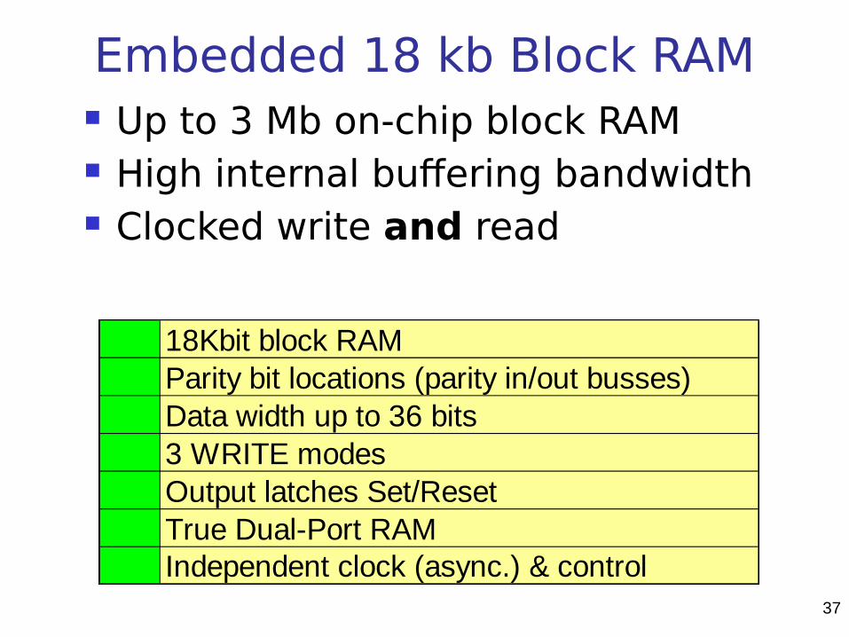
Embedded 18 kb Block RAM Up to 3 Mb on-chip block RAM High internal buffering bandwidth Clocked write and read
18Kbit block RAMParity bit locations (parity in/out busses)Data width up to 36 bits3 WRITE modesOutput latches Set/ResetTrue Dual-Port RAMIndependent clock (async.) & control

38
Configurations available on each port:
True Dual-Port™ Configurations
Independent port A and B configuration: Support for data
width conversion including parity bits
Port A: 8-bIN 8-bit
OUT 32-bitPort B: 32-b
IN 8-bit
IN 8-bit
IN 8
-bit
IN 8
-bi t
ADDRB
ADDRA
Configuration Depth Data bits Parity bits16K x 1 16Kb 1 08K x 2 8Kb 2 04K x 4 4Kb 4 02K x 9 2Kb 8 11K x 18 1Kb 16 2512 x 36 512 32 4

How to
39
RAMB16_S36_S36 inmem (// port A .CLKA(wb.clk), .SSRA(wb.rst), .ADDRA(bram_addr), .DIA(bram_data), .DIPA(4'h0), .ENA(bram_ce), .WEA(bram_we), .DOA(doa), .DOPA(), // port B .CLKB(wb.clk), .SSRB(wb.rst), .ADDRB({3'h0,rdc}), .DIB(32'h0), .DIPB(4'h0), .ENB(1'b1),.WEB(1'b0), .DOB(dob), .DOPB());
Block RAM : just instantiate template2-port 512x32(+4)
32
32
9
32
32
9BRAM
8
8
11
32
32
9BRAM
RAMB16_S9_S36 inmem (// port A … // port B … );
2048x8 512x32

40
Virtex-II LUT can implement: 16 x 1-bit synchronous RAM Synchronous write Asynchronous read
D flip-flop in the same slice can register the output Allow fast embedded RAM of any width
Only limited by the number of slices in each device
Example: RAM 16 x 48-bit fits in 48 LUTs
Distributed RAM

How to
41
Distributed RAM : 16 LUTs2-adr 16x8
logic [7:0] mem0[0:15];
always_ff @(posedge clk) if (wr) begin
mem0[addra] <= d_i; end
assign db_o = (rdb) ? {mem0[addrb] : 8'h0;assign da_o = (rda) ? {mem0[addra] : 8'h0;
8
4
8
4dRAM
8
Distributed RAM : 8 LUTs 1-adr 16x8
8
4
8
dRAM
logic [7:0] mem0[0:15];
always_ff @(posedge clk) if (wr) begin
mem0[addr] <= d_i; end
assign d_o=(rd) ? mem0[addr] : 8'h0;
addr
d_i
d_o
addra addrb
d_i
da_o db_o

42
18 x 18Multiplier
Output (36 bits)
Data_A (18 bits)
Data_B (18 bits)
18 x 18 Multiplier Embedded 18-bit x 18-bit multiplier
2’s complement signed operation Multipliers are organized in columns

43
An example: a decade counter
module dec( input clk,rst output u);
reg u; reg [3:0] q;
always_ff @(posedge clk or posedge rst) if (rst)
q <= 4'h0;else if (q == 9) q <= 4'h0;else q <= q+1;
always_ff @(posedge clk) if (q == 9)
u <= 1'b1;else u <= 1'b0;
endmodule

44

45
urst
clk
2 slices

46
2 slices = 4 LUTs
LUT
q0
q1
q2
q3
LUT
q0
q1
q2
q3
LUT
q0
q1
q2
q3
LUT
q0
q0
q1
q2
q3
q0
q1
q2
q3
u+
padu+ u
I/O-buffer
0123011 )( qqqqqqq