Embed Size (px)
Citation preview
DS579 December 14, 2010 www.xilinx.com 1Product Specification
© Copyright 2007-2010 Xilinx, Inc. XILINX, the Xilinx logo, Virtex, Spartan, ISE and other designated brands included herein are trademarks of Xilinx in the United States and other countries. The PowerPC name and logo are registeed trademarks of IBM Corp. and are used under license. All other trademarks are the property of their respective owners.
IntroductionThe XPS Central DMA Controller provides simpleDirect Memory Access (DMA) services to peripheralsand memory devices on the PLB. The controllertransfers a programmable quantity of data from asource address to a destination address withoutprocessor intervention.
Features• Connects as a 32-bit master/slave on PLB V4.6
buses of 32, 64 or 128 bits
• Provides a single physical channel of Direct Memory Access between a source address and a destination address
• Provides programmable registers for source address, destination address and transfer length
• Parameterizable local FIFO depth and burst length
• Supports different clock domains for Master and Slave interfaces
• The source address and destination address can be arbitrarily aligned (down to the byte)
• Supports overlapped PLB read/write transfers which will give better performance
• Supports unaligned address transfers
• Supports setting up of source and destination addresses as incrementing or fixed (keyhole)
• Supports PLB burst transfers
LogiCORE IP XPS Central DMAController (v2.03a)
DS579 December 14, 2010 Product Specification
LogiCORE™ IP Facts Table
Core Specifics
Supported Device Family(1)
Spartan®-3, Spartan-3E, Spartan-3A, Spartan-6, Spartan-3A DSP, Automotive Spartan-3/3A/3A DSP/ 3E, Virtex®-4, Virtex-4Q, Virtex-4QV, Virtex-5/5FX, Virtex-6/6CX
Supported User Interfaces PLBv46
Resources
Block RAMSFor Virtex-5 FPGA, see Table 14, for Virtex-5 FPGA, see Table 15, for Spartan-3E, see Table 16, for Virtex-6 FPGA, see Table 17. and for Spartan-6 FPGA, see Table 18.
LUTs
Slices
FFs
Provided with Core
Documentation Product Specification
Design Files VHDL
Example Design Not Provided
Test Bench Not Provided
Constraints File Not Provided
Simulation Model N/A
Tested Design Tools
Design Entry Tools Platform Studio
Simulation Mentor Graphic ModelSim v6.5c and above
Synthesis Tools XST
Support
Provided by Xilinx, Inc.
Notes: 1. For a complete listing of supported devices, see the release
notes for this core.

DS579 December 14, 2010 www.xilinx.com 2Product Specification
LogiCORE IP XPS Central DMA Controller (v2.03a)
Functional DescriptionThe block diagram for the XPS Central DMA Controller is shown in Figure 1. The core is comprised of the followingprimary modules which are described in the subsequent sections:
• Slave Attachment Module
• Master Attachment Module
• FIFO
• DRE.
Slave Attachment
The Slave Attachment module performs the following operations:
• Interfaces with the PLB V4.6 using the PLB Interface Module.
• Responds to PLB transactions to read and write the DMA registers.
• Modifies the Source Address, Destination Address, Length, DMA Status and Interrupt Status Registers as a DMA operation proceeds.
• Generates interrupts based on DMA done and DMA error conditions, detected in the Master Attachment Module.
Master Attachment
The Master Attachment module performs the following operations:
• Performs read and write transactions as a PLB master to transfer the amount of data specified in the Length Register from source address to destination address, using bursts where appropriate.
• Detects errors.
• Updates the Source Address, Destination Address, Length and DMA Status Registers during the DMA transfer.
X-Ref Target - Figure 1
Figure 1: Block Diagram for the XPS Central DMA Controller
RST
ISR
IER
SA
DA
DMACR
DMASR
LENGTH
PLBInterfaceModule
Slave Attachment Module
IP2INTC_lrpt
XPS Central DMA Controller
PLBMaster
InterfaceMasterAttachment
Module
FIFO DRE
Read/Write Enable
PLBv4.6
PLBSlave
Interface
PLBv4.6
DS579_01_041910

DS579 December 14, 2010 www.xilinx.com 3Product Specification
LogiCORE IP XPS Central DMA Controller (v2.03a)
DRE
The DRE (Data Realignment Module) will align the unaligned data before writing in to the FIFO from the sourceaddress or to write in to the destination address from the FIFO.
FIFO
XPS Central DMA Controller contains a 32-bit FIFO:
• Stores the data to be transferred locally.
• The depth of the FIFO can be configured to 1, 16, 32 and 48.
• The FIFO enables the simultaneous read and write transactions based on its vacancy and occupancy.
Controller OperationThe XPS Central DMA Controller operates on the PLB using independent master and slave interfaces. It respondsas a slave when its registers are being read and written. It initiates read and write transactions as a master when aDMA operation is in progress.
Although it is common to connect the master and slave interfaces to the same bus, it is possible, as shown inFigure 1, to connect them to different PLB buses, possibly operating at different frequencies. Frequency ratios of 1:1,2:1 and 1:2 between master and slave bus clocks are supported.
Note: The design accommodates arbitrary clock relationships, including uncorrelated clocks, but the core is specified and tested for the given ratios only.
The master and slave connections of the XPS Central DMA operate as 32-bit PLB agents. However, either the masteror slave can connect to a PLB with wider data paths (64-bit or 128-bit) and conduct transactions with wider slavesor masters.
The operation of the XPS Central DMA is initiated by writing values into the following DMA registers. For moreinformation, see the Register Descriptions.
• Source Address register (SA): The source address for the transfer is written into this register.
• Destination Address register (DA): The destination address for the transfer is written into this register.
• DMA Control Register (DMACR): The parameters of the DMA transfer are controlled by setting the following values in this register.
• Source Increment (SINC): SINC should be set to ’0’, if and only if the Source Address register is written with a keyhole address such that a single address is associated with a sequence of data.
Note: An example of a keyhole address is a memory mapped FIFO that maps as an element at a single address but can consume or produce an endless sequence of data. A variation on a keyhole address is a wide keyhole where a number of consecutive addresses map to the element. When SINC = ’0’, XPS Central DMA will perform all read transactions to the same address. It is the responsibility of the corresponding slave to impose a keyhole behavior. For bursts, this implies that the slave will not increment the keyhole address during the burst or will make the keyhole at least as wide as the burst size. It is not feasible to use SINC = ’0’ with a non-keyhole slave such as a memory. Even though the DMA Controller would deliver a non-incremented address during the address phase of PLB transactions, the memory would increment it during bursts. (See also DINC, which is subject to the same considerations when set to ’0’.)
• If the source address should increment for each data transferred, SINC should set to ’1’.
• Destination Increment (DINC): DINC should be set to ’0’ if and only if the Destination Address is written with a keyhole address such that a single address is associated with a sequence of data.
Note: See the note for SINC = ‘0’ above. The case DINC = ‘0’ has the same considerations except for the destination address.
• If the destination address should increment for each data transferred, DINC should set to ’1’.
DS579 December 14, 2010 www.xilinx.com 4Product Specification
LogiCORE IP XPS Central DMA Controller (v2.03a)
• LENGTH register (LENGTH): The number of bytes to transfer is written into this register. Writing to this register is the event that starts the DMA operation, so it must be done last. (Refer to Table 10 for more information on this register)
The data transfer starts by reading data from the source address into an internal FIFO followed by the transfer ofdata from the FIFO to the destination address. This repeats until all the data is moved. The DMA Status Registersget updated as the DMA operation progresses.
While it is moving data as the bus master, the XPS Central DMA Controller attempts to move data efficiently. Itutilizes burst transactions where possible.
The status of the DMA operation is available in the DMA Status Register (DMASR). The DMABSY bit equal to ’1’represents that a DMA operation is underway. When equal to ’0’, it represents the completion of a DMA transfer.Alternatively, the DMA Done (DD) interrupt can be used to detect when a DMA operation is complete.
If an error condition is detected during a bus transfer, the DMA operation will be aborted at its current point ofprogress. The error is reported through the DMA Error (DE) interrupt condition and the DMA Bus Error (DBE)status bit.
Interrupt and Error Condition Descriptions
DMA Interrupt Conditions
Interrupt conditions, which are established by the occurrence of interrupt events, are stored in the Interrupt StatusRegister of the channel (see Table 12). Interrupt conditions can be reported, cleared and enabled.
• Reporting: Port signal IP2INTC_Irpt is active if and only if either of the interrupt conditions occurs.
• Clearing: Active interrupt conditions are cleared by writing a value to the Interrupt Status Register with a 1 in the bit position to be cleared.
• Enabling: Interrupts are enabled by setting the corresponding bit in the Interrupt Enable Register. (see Table 13)
Error Conditions
A DMA operation proceeds until it is complete or until it is aborted due to an error condition detected on the bus.
If completion is due to an error, the corresponding DMA BUS Error (DBE) bit of the DMA Status Register (DMASR)will be set. Additionally, the DMA Error (DE) interrupt condition will become active. The final values of LENGTH,SA and DA will reflect the partial completion status of the DMA operation, taking into account that unwritten datawill be flushed out by resetting the internal FIFO.

DS579 December 14, 2010 www.xilinx.com 5Product Specification
LogiCORE IP XPS Central DMA Controller (v2.03a)
I/O SignalsThe XPS Central DMA Controller I/O signals are listed and described in Table 1. All signals are active high.
Table 1: I/O Signal Description
Port Signal Name Interface I/O Initial State Description
PLB Master Interface Signals
P1 MPLB_Clk PLB I - PLB master clock
P2 MPLB_Rst PLB I - PLB master reset
P3 M_ABus[0:C_MPLB_AWIDTH - 1] PLB O 0 Master address bus
P4 M_BE[0:C_MPLB_DWIDTH/8 - 1] PLB O 0 Master byte enables
P5 M_wrDBus[0:C_MPLB_DWIDTH - 1] PLB O 0 Master write data bus
P6 M_request PLB O 0 Master bus request
P7 M_RNW PLB O 0 Master read not write
P8 M_priority[0:1] PLB O 0 Master bus request priority
P9 M_rdBurst PLB O 0 Master burst read transfer indicator
P10 M_type[0:2] PLB O 0 Master transfer type
P11 M_size[0:3] PLB O 0 Master transfer size
P12 M_wrBurst PLB O 0 Master burst write transfer indicator
P13 M_MSize[0:1] PLB O 0 Master data bus size
P14 MPLB_MRdDBus[0:C_MPLB_DWIDTH - 1] PLB I - PLB master read data bus
P15 MPLB_MBusy PLB I - PLB master slave busy indicator
P16 MPLB_MRdErr PLB I - PLB master slave read error indicator
P17 MPLB_MWrErr PLB I - PLB master slave write error indicator
P18 MPLB_MWrBterm PLB I - PLB master terminate write burst indicator
P19 MPLB_MWrDAck PLB I - PLB master write data acknowledge
P20 MPLB_MAddrAck PLB I - PLB master address acknowledge
P21 MPLB_MRdBTerm PLB I - PLB master terminate read burst indicator
P22 MPLB_MRdDAck PLB I - PLB master read data acknowledge
P23 MPLB_MRearbitrate PLB I - PLB master bus rearbitrate indicator
P24 M_TAttribute[0:15] PLB O 0 Master Transfer Attribute bus
P25 M_UABus[0:31] PLB O 0 Master upper address bus
P26 M_lockErr PLB O 0 Master lock error indicator
P27 M_BusLock PLB O 0 Master bus lock
P28 M_abort PLB O 0 Master abort bus request indicator
P29 MPLB_MRdWdAddr[0:3] PLB I - PLB master read word address

DS579 December 14, 2010 www.xilinx.com 6Product Specification
LogiCORE IP XPS Central DMA Controller (v2.03a)
P30 MPLB_MSSize[0:1] PLB I - PLB slave data bus size
P31 MPLB_MTimeout PLB I - PLB master bus time out
P32 MPLB_MIRQ PLB I - PLB master slave interrupt indicator
PLB Slave Interface Signals
P33 SPLB_Clk PLB I - PLB clock
P34 SPLB_Rst PLB I - PLB reset
P35 SPLB_ABus[0:C_SPLB_AWIDTH - 1] PLB I - PLB address bus
P36 SPLB_type[0:2] PLB I - PLB transfer type
P37 SPLB_size[0:3] PLB I - PLB transfer size
P38 SPLB_abort PLB I - PLB abort bus request indicator
P39 SPLB_rdBurst PLB I - PLB burst read transfer indicator
P40 SPLB_wrBurst PLB I - PLB burst write transfer indicator
P41 SPLB_BE[0:C_SPLB_DWIDTH/8 - 1] PLB I - PLB byte enables
P42 SPLB_wrDBus[0:C_SPLB_DWIDTH - 1] PLB I - PLB write data bus
P43 SPLB_RNW PLB I - PLB read not write
P44 SPLB_PAValid PLB I - PLB primary address valid indicator
P45 SPLB_SAValid PLB I - PLB secondary address valid indicator
P46 SPLB_masterID[0:C_SPLB_MIDWIDTH - 1] PLB I - PLB current master identifier
P47 SPLB_rdPrim PLB I - PLB secondary to primary read request indicator
P48 SPLB_wrPrim PLB I - PLB secondary to primary write request indicator
P49 SPLB_busLock PLB I - PLB lock
P50 SPLB_MSize[0:1] PLB I - PLB master data bus size
P51 SPLB_UABus[0:31] PLB I - PLB upper address bus
P52 SPLB_reqpri[0:1] PLB I - PLB current request priority
P53 SPLB_TAttribute[0:15] PLB I - PLB Transfer Attribute bus
P54 SPLB_lockerr PLB I - PLB lock error indicator
P55 SPLB_rdpendPri[0:1] PLB I - PLB pending read request priority
P56 SPLB_wrpendPri[0:1] PLB I - PLB pending write request priority
P57 SPLB_rdpendReq PLB I - PLB pending bus read request indicator
P58 SPLB_wrpendReq PLB I - PLB pending bus write request indicator
P59 Sl_rdDBus[0:C_SPLB_DWIDTH - 1] PLB O 0 Slave read data bus
Table 1: I/O Signal Description (Cont’d)
Port Signal Name Interface I/O Initial State Description
DS579 December 14, 2010 www.xilinx.com 7Product Specification
LogiCORE IP XPS Central DMA Controller (v2.03a)
Design ParametersTo allow the user to create a XPS Central DMA Controller that is uniquely tailored for the user’s system, certainfeatures are parameterizable in the XPS Central DMA Controller design. This allows the user to have a design thatutilizes only the resources required by the system and runs at the best possible performance. The features that areparameterizable in the XPS Central DMA core are as shown in Table 2.
P60 Sl_addrAck PLB O 0 Slave address acknowledge
P61 Sl_SSize[0:1] PLB O 0 Slave data bus size
P62 Sl_MWrErr[0:C_SPLB_NUM_MASTERS - 1] PLB O 0 Slave write error indicator
P63 Sl_MRdErr[0:C_SPLB_NUM_MASTERS - 1] PLB O 0 Slave read error indicator
P64 Sl_wait PLB O 0 Slave wait indicator
P65 Sl_rearbitrate PLB O 0 Slave rearbitrate bus indicator
P66 Sl_wrDAck PLB O 0 Slave write data acknowledge
P67 Sl_wrComp PLB O 0 Slave write transfer complete indicator
P68 Sl_rdDAck PLB O 0 Slave read data acknowledge
P69 Sl_rdComp PLB O 0 Slave read transfer complete indicator
P70 Sl_MBusy[0:C_SPLB_NUM_MASTERS - 1] PLB O 0 Slave busy indicator
P71 Sl_wrBTerm PLB O 0 Slave terminate write burst transfer
P72 Sl_rdWdAddr[0:3] PLB O 0 Slave read word address
P73 Sl_rdBTerm PLB O 0 Slave terminate read burst transfer
P74 Sl_MIRQ[0:C_SPLB_NUM_MASTERS - 1] PLB O 0 Slave interrupt indicator
System Signals
P75 IP2INTC_Irpt System O 0 DMA Interrupt
Table 1: I/O Signal Description (Cont’d)
Port Signal Name Interface I/O Initial State Description

DS579 December 14, 2010 www.xilinx.com 8Product Specification
LogiCORE IP XPS Central DMA Controller (v2.03a)
Table 2: Design Parameters
Generic Feature/Description Parameter Name Allowable Values DefaultValue VHDL Type
System Parameter
G1 Target FPGA family C_FAMILY
aspartan3, spartan3, spartan3a, spartan3e, aspartan3a, aspartan3e, aspartan3a, aspartan3adsp, spartan6, virtex4, qrvirtex4, qvirtex4, virtex5, virtex6
virtex5 string
PLB Parameters
G2 XPS Central DMA Controller Base Address C_BASEADDR Valid Address(1) None(2) std_logic_vector
G3 XPS Central DMA Controller High Address C_HIGHADDR Valid Address(1) None(2) std_logic_vector
G4 PLB master data width C_MPLB_DWIDTH 32,64,128 32 integer
G5 PLB master address width C_MPLB_AWIDTH 32 32 integer
G6 PLB address width C_SPLB_AWIDTH 32 32 integer
G7 PLB data width C_SPLB_DWIDTH 32, 64, 128 32 integer
G8
Selects point-to-point or shared PLB topology0 = Shared Bus Topology1 = Point-to-Point Bus Topology
C_SPLB_P2P 0 0 integer
G9 PLB Master ID Bus Width
C_SPLB_MID_WIDTH
log2(C_SPLB_NUM_MASTERS) with a minimum value of 1
1 integer
G10 Number of PLB Masters C_SPLB_NUM_MASTERS 1 - 16 1 integer
G11 Width of the Slave Data Bus
C_SPLB_NATIVE_DWIDTH 32 32 integer
G12 Burst support C_SPLB_SUPPORT_BURSTS 0 0 integer
G13 Width of the Master Data Bus
C_MPLB_NATIVE_DWIDTH 32 32 integer
XPS Central DMA Controller Feature
G14 FIFO Depth(3) C_FIFO_DEPTH 1, 8, 16, 32, 48 16 integer
G15 Read Burst Size(4) C_RD_BURST_SIZE 1, 8, 16 16 integer
G16 Write Burst Size(4) C_WR_BURST_SIZE 1, 8, 16 16 integer
Notes: 1. C_BASEADDR must be a multiple of the address-range size, where the size is C_HIGHADDR - C_BASEADDR + 1.2. No default value will be specified to insure that the actual value is set.3. FIFO Depth should be greater than or equal to the Read Burst Size and Write Burst Size4. Read Burst Size should be greater than or equal to the Write burst Size

DS579 December 14, 2010 www.xilinx.com 9Product Specification
LogiCORE IP XPS Central DMA Controller (v2.03a)
Allowable Parameter Combinations
The address-range size specified by C_BASEADDR and C_HIGHADDR must be a power of 2, and must be at least0x40. For example, if C_BASEADDR = 0xE0000000, C_HIGHADDR must be at least = 0xE000003F.
C_PLB_MIDWIDTH depends on C_PLB_NUM_MASTERS. It must be set to the maximum of 1 or the smallestinteger greater than or equal to log2(C_PLB_NUM_MASTERS).
Below table shows the valid combinations among C_FIFO_DEPTH, C_RD_BURST_SIZE and C_WR_BURST_SIZE.If C_RD_BURST_SIZE = C_WR_BURST_SIZE and C_FIFO_DEPTH >= 2X of C_RD_BURST_SIZE will give betterperformance in terms of latency. The user has the flexibility in choosing these parameters depending on the systemrequirements.
Parameter - Port DependenciesThe dependencies between the XPS Central DMA core design parameters and I/O signals are described in Table 4.In addition, when certain features are parameterized out of the design, the related logic will no longer be a part ofthe design. The unused input signals and related output signals are set to a specified value.
Table 3: Allowable FIFO Depth, Read and Write Burst Size Parameters
C_FIFO_DEPTH C_RD_BURST_SIZE C_WR_BURST_SIZE
1 1 1
8 8 1
8 8 8
16 8 8
16 8 1
16 16 1
16 16 8
16 16 16
32 8 1
32 8 8
32 16 1
32 16 8
32 16 16
48 8 1
48 8 8
48 16 1
48 16 8
48 16 16

DS579 December 14, 2010 www.xilinx.com 10Product Specification
LogiCORE IP XPS Central DMA Controller (v2.03a)
Table 4: Design Parameter - Port Dependencies
Generic or Port Name Affects Depends Relationship Description
Design Parameters
G4 C_MPLB_DWIDTH P4,P5,P14 - Affects number of bits in master data bus.
G6 C_SPLB_AWIDTH P35 Affects number of bits in address bus.
G7 C_SPLB_DWIDTH P41,P42,P59 - Affects number of bits in data bus.
G9 C_SPLB_MID_WIDTH P46 G10Affects the width of current master identifier signals and depends on log2(C_SPLB_NUM_MASTERS) with a minimum value of 1.
G10 C_SPLB_NUM_MASTERS
P62,P63,P70,P74 - Affects the width of busy and error signals.
I/O Signals
P3 M_ABUS[0:C_MPLB_AWIDTH] - G5 Width varies with the size of the PLB master address
bus.
P4 M_BE[0:C_MPLB_DWIDTH/8 - 1] - G4 Width varies with the size of the PLB master data bus.
P5 M_wrDBus[0:C_MPLB_DWIDTH - 1] - G4 Width varies with the size of the PLB master data bus.
P14 MPLB_MRdDBus[0:C_MPLB_DWIDTH - 1] - G4 Width varies with the size of the PLB master data bus.
P35 SPLB_ABus[0:C_SPLB_AWIDTH - 1] - G6 Width varies with the size of the PLB address bus.
P41 SPLB_BE[0:C_SPLB_DWIDTH/8 - 1] - G7 Width varies with the size of the PLB data bus.
P42 SPLB_wrDBus[0:C_SPLB_DWIDTH - 1] - G7 Width varies with the size of the PLB data bus.
P46 SPLB_masterID[0:C_SPLB_MIDWIDTH - 1] G9 Width varies with the size of the PLB number of
masters.
P59 Sl_rdDBus[0:C_SPLB_DWIDTH - 1] - G7 Width varies with the size of the PLB data bus.
P62 Sl_MWrErr[0:C_SPLB_NUM_MASTERS - 1] - G10 Width varies with the size of the PLB number of
masters.
P63 Sl_MRdErr[0:C_SPLB_NUM_MASTERS - 1] - G10 Width varies with the size of the PLB number of
masters.
P70 Sl_MBusy[0:C_SPLB_NUM_MASTERS - 1] - G10 Width varies with the size of the PLB number of
masters.
P74 Sl_MIRQ[0:C_SPLB_NUM_MASTERS - 1] - G10 Width varies with the size of the PLB number of
masters.

DS579 December 14, 2010 www.xilinx.com 11Product Specification
LogiCORE IP XPS Central DMA Controller (v2.03a)
Register DescriptionsTable 5 shows the XPS Central DMA Controller registers and their addresses. The remaining unused addresses inthe address-range size are reserved. Writing into the reserved registers has no effect. Reading of the reservedregisters returns zero. Each register is addressable on a 32-bit boundary. All registers are defined for 32-bit accessonly. Any partial word access (byte, half-word) has undefined results and return a bus error. The detailedinformation about these registers is provided in the following section. The register addresses are offset to the baseaddress, C_BASEADDR.
Software Reset Register (RST)
The Software Reset Register (RST) is shown in Figure 2. It is a write only register addressed at an offset 0x0 frombase address C_BASEADDR. The bit definitions of this register are as shown in Table 6.
Table 5: Controller Registers
Register Name Base Address + Offset (hex) Default Value (hex) Access
Software Reset Register (RST) C_BASEADDR + 0 NA Write (1)
DMA Control Register (DMACR)(2) C_BASEADDR + 4 80000000 R/W
Source Address (SA)(2) C_BASEADDR + 8 00000000 R/W
Destination Address (DA)(2) C_BASEADDR + C 00000000 R/W
Length (LENGTH)(2) C_BASEADDR +10 00000000 R/W
DMA Status Register (DMASR) C_BASEADDR + 14 00000000 Read (3)
Interrupt Status Register (ISR)(2) C_BASEADDR + 2C 00000000 Read/TOW(4)
Interrupt Enable Register (IER)(2) C_BASEADDR + 30 00000000 R/W
1. Reading of this register returns zero.2. These registers are guaranteed to return a consistent value only if read when XPS Central DMA Controller is idle. Inconsistent
values can be returned when these registers are sampled in SPLB clock domain while it is changing in the MPLB clock domain.3. Writing into this register has no effect.4. TOW =Toggle On Write. Writing a ’1’ to a bit position within the register causes the corresponding bit position in the register to
toggle.
X-Ref Target - Figure 2
Figure 2: Software Reset Register (RST)
Table 6: RST Register Bit Definitions
Bits Name CoreAccess
ResetValue Description
0 - 31 RST Write N/A
Software ResetA write of 0x0000000A causes reset of the XPS Central DMA Controller. A write of any other value has undefined effect and returns a bus error. A read of this register returns zero.
0 31
RST
DS579_02_041910

DS579 December 14, 2010 www.xilinx.com 12Product Specification
LogiCORE IP XPS Central DMA Controller (v2.03a)
DMA Control Register (DMACR)
The DMA Control Register (DMACR) is shown in Figure 3. It is a read/write register addressed at an offset 0x4from base address C_BASEADDR. The bit definitions of this register are as shown in Table 7.
Source Address Register (SA)
The Source Address Register (SA) is shown in Figure 4. It is a read/write register addressed at an offset 0x8 frombase address C_BASEADDR. The bit definitions of this register are as shown in Table 8.
X-Ref Target - Figure 3
Figure 3: DMA Control Register (DMACR)
Table 7: DMACR Bit Definitions
Bits Name CoreAccess
ResetValue Description
0 SINC R/W ’1’
Source Increment: Increment the source address by the number of source bytes read. ’1’ = Increment the source address.’0’ = Do not increment the source address. SINC = ’0’ is allowed if and only if the Source Address register is written with a keyhole address. See also the An example of a keyhole address note on page 3.
1 DINC R/W ’0’
Destination Increment: Increment the destination address by the number of bytes written in to the destination. ’1’ = Increment the destination address’0’ = Do not increment the destination address. DINC = ’0’ is allowed if and only if the Destination Address register is written with a keyhole address. See also The case DINC = ‘0’ note on page 3.
2 - 31 Reserved
X-Ref Target - Figure 4
Figure 4: Source Address Register (SA)
Table 8: SA Register Bit Definitions
Bits Name CoreAccess
ResetValue Description
0 - 31 SA R/W 0
Source Address: Source address for the current DMA operation. When SINC = ’1’, as data is moved from the source address, this register updates to track the current source address. When SINC = ’0’, the source address remains constant at the programmed value. (See also the SINC field of the DMA Control Register).
20 31
Reserved
1
SINC
DINC DS579_03_041910
0 31
SA
DS579_04_041910

DS579 December 14, 2010 www.xilinx.com 13Product Specification
LogiCORE IP XPS Central DMA Controller (v2.03a)
Destination Address Register (DA)
The Destination Address Register (DA) is shown in Figure 5. It is a read/write register addressed at an offset 0xCfrom base address C_BASEADDR.The bit definitions of this register are as shown in Table 9.
Length Register (LENGTH)
Length Register (LENGTH) is shown in Figure 6. It is a read/write register addressed at an offset 0x10 from baseaddress C_BASEADDR. The bit definitions of this register are as shown in Table 10.
X-Ref Target - Figure 5
Figure 5: Destination Address Register (DA)
Table 9: DA Register Bit Definitions
Bits Name CoreAccess
ResetValue Description
0 - 31 DA R/W 0
Destination Address: Destination address for the current DMA operation. When DINC = ’1’, as data is moved to the destination address, this register updates to track the current destination address. When DINC = ’0’, the destination address remains constant at the programmed value. (See also the DINC field of the DMA Control Register.)
X-Ref Target - Figure 6
Figure 6: Length Register (LENGTH)
Table 10: LENGTH Register Bit Definitions
Bits Name CoreAccess
ResetValue Description
0 - 31 LENGTH (1) R/W 0
Length of the DMA Transfer: The DMA operation starts when the number of bytes to be transferred from source to destination is written to the Length Register. Therefore, this register is written only after the DMA Control register, the Source Address and the Destination Address registers have been written with their desired values and any other setup is complete. As bytes are successfully written to the destination, the Length Register decrements to reflect the number of bytes remaining to be transferred. The Length Register will be zero after a successful DMA operation.
1. If the written value is not a multiple of DSIZE, the transfer is a mix of byte as well as a word transfers. For example, if the Length Register is programmed to ten bytes, the XPS Central DMA Controller will transfer the two bytes using the byte enables as a single transfer. The remaining eight bytes will be transferred as two data word burst. The final value of the Length Register will be zero.
0 31
SA
DS579_05_041910
0 31
LENGTH
DS579_06_041910

DS579 December 14, 2010 www.xilinx.com 14Product Specification
LogiCORE IP XPS Central DMA Controller (v2.03a)
DMA Status Register (DMASR)
The DMA Status Register (DMASR) is shown in Figure 7. It is a read only register addressed at an offset 0x14 frombase address C_BASEADDR. A write to this register has no effect. The bit definitions of this register are as shownin Table 11..
Interrupt Status Register (ISR)
The Interrupt Status Register (ISR) is shown in Figure 8. It is a read/toggle-on-write register addressed at an offset0x2C from base address C_BASEADDR. The bit definitions of this register are as shown in Table 12. The interruptstatus bits are set whenever their corresponding condition holds. The corresponding interrupt enable bit set as false(see Table 13) does not inhibit ISR reporting but does inhibit assertion of the interrupt signal, IP2INTC_Irpt, inresponse to the interrupt status bit.
X-Ref Target - Figure 7
Figure 7: DMA Status Register (DMASR)
Table 11: DMASR Bit Definitions
Bits Name CoreAccess
Reset Value Description
0 DMABSY Read ’0’DMA Busy:’0’ = DMA operation is not in progress.’1’ = DMA operation is in progress.
1 DBE Read ’0’DMA Bus Error:’0’ = No DMA bus error.’1’ = DMA bus error.
2 - 31 Reserved
X-Ref Target - Figure 8
Figure 8: Interrupt Status Register (ISR)
Table 12: ISR Bit Definitions
Bits Name Core Access Reset Value Description
0 - 29 Reserved
30 DE R/TOW ’0’DMA Error:’0’ = DMA error has not occurred.’1’ = DMA error has occurred.
31 DD R/TOW ’0’DMA Done:’0’ = DMA operation is not done.’1’ = DMA operation is done.
0
Reserved
1
DMABSY
DBE
31
DS579_07_041910
31
Reserved DE
DD
300
DS579_08_041910

DS579 December 14, 2010 www.xilinx.com 15Product Specification
LogiCORE IP XPS Central DMA Controller (v2.03a)
Interrupt Enable Register (IER)
The Interrupt Enable Register (IER) is shown in Figure 9. It is a read/write register addressed at an offset 0x30 frombase address C_BASEADDR. The bit definitions of this register are as shown in Table 13. These bits inhibit assertionof the IP2INTC_Irpt signal in response to the corresponding interrupt status bit (see Table 12).
Timing DiagramsThe following timing diagrams illustrate the XPS Central DMA Controller operation for various read and writetransactions of different lengths.
1. Read and write transactions of a 32-bit aligned DMA transfer of length 32 bytes are shown in Figure 10.
2. Read and write transactions of a time-out case in a 32-bit aligned DMA transfer of length 8 bytes are shown in Figure 11 and Figure 12.
X-Ref Target - Figure 9
Figure 9: Interrupt Enable Register (IER)
Table 13: IER Bit Definitions
Bits Name Core Access
Reset Value Description
0 - 29 Reserved
30 DEIE R/W ’0’DMA Error Interrupt Enable: Interrupt enable bit for DMA error. ’0’ = IP2INTC_Irpt will not assert in response to DMA Error interrupt status.’1’ = IP2INTC_Irpt will assert in response to DMA Error interrupt status.
31 DDIE R/W ’0’DMA Done Interrupt Enable: Interrupt enable bit for DMA done.’0’ = IP2INTC_Irpt will not assert in response to DMA Done interrupt status.’1’ = IP2INTC_Irpt will assert in response to DMA Done interrupt status.
31
Reserved DEIE
DDIE
300
DS579_09_041910

DS579 December 14, 2010 www.xilinx.com 16Product Specification
LogiCORE IP XPS Central DMA Controller (v2.03a)
X-Ref Target - Figure 10
Figure 10: Transaction for 32-bit Aligned DMA Transfer of Length 32
X-Ref Target - Figure 11
Figure 11: Read Time Out for 32-bit Aligned DMA Transfer of Length 8
Cycles
PLB_Clk
M_ABus[0:31]
PLB_PAValid
MPLB_MAddrAck
M-size[0:3]
M_BE[0:3]
MPLB_MRdDBus[0:31]
MPLB_MRdDAck
M_RNW
M_rdBurst
MPLB_MRdBTerm
M_wrDBus[0:31]
MPLB_MWrDAck
M_wrBurst
MPLB_MWrBTerm
1 2 3 4 5 6 7 8 9 10 1112 13 14 15 1617 18 19 2021 22 23 24 2526 27 28 29 3031 32 33 3435 36
30000004
1010
1111
SourceAddress
D 0 D 1
D 2
D 3
D 4
D 5 D 6 D 7
38 39 40 41 42 43 44 45 4647
40000004
1010
1111
D0 D1 D2 D4 D5 D6 D7
D 3
DestinationAddress
D0 : The first of the 4 bytes of data tranferred from Source Address(SA) to Destiantion Address(DA)D1 : The second 4 bytes of data transferred from SA + 0x4 to DA + 0x4D2 : The third 4 bytes of data transferred from SA + 0x8 to DA + 0x8D3 : The fourth 4 bytes of data transferred from SA + 0xC to DA + 0xCD4 : The fifth 4 bytes of data transferred from SA + 0x10 to DA + 0x10D5 : The sixth 4 bytes of data transferred from SA + 0x14 to DA+ 0x14D6 : The seventh 4 bytes of data transferred from SA + 0x18 to DA + 0x18D7 : The last 4 bytes of data transferred from SA + 0x1C to DA + 0x1C
37
DS579_10_041910
Cycles
PLB_Clk
M_ABus[0:31]
PLB_PAValid
MPLB_MAddrAck
MPLB_MTimeout
M_size[0:3]
M_BE[0:3]
MPLB_MRdDBus[0:31]
MPLB_MRdDAck
M_RNW
M_rdBurst
MPLB_MRdBTerm
M_wrDBus[0:31]
MPLB_MWrDAck
M_wrBurst
MPLB_MWrBTerm
1 2 3 4 5 6 7 8 9 10 11 12 13 14 15 16 17 18 19 20 21 22 23
10000000
00001111
SourceAddress
DS579_11_041910

DS579 December 14, 2010 www.xilinx.com 17Product Specification
LogiCORE IP XPS Central DMA Controller (v2.03a)
Design Implementation
Target Technology
The intended target technology is an FPGA listed in the Supported Device Family field of the LogiCORE™ IP FactsTable.
Device Utilization and Performance Benchmarks
Core Performance
Because the XPS Central DMA Controller core will be used with other design modules in the FPGA, the utilizationand timing numbers reported in this section are estimates only. When this core is combined with other designs inthe system, the utilization of FPGA resources and timing of the XPS Central DMA Controller design will vary fromthe results reported here.
X-Ref Target - Figure 12
Figure 12: Write Time Out for 32-bit Aligned DMA Transfer of Length 8
Cycles
PLB_Clk
M_ABus[0:31]
PLB_PAValid
MPLB_MAddrAckMPLB_MTimeout
M_size[0:3]
M_BE[0:3]
MPLB_MRdDBus[0:31]
MPLB_MRdDAck
M_RNW
M_rdBurst
MPLB_MRdBTerm
M_wrDBus[0:31]
MPLB_MWrDAck
M_wrBurst
MPLB_MWrBTerm
1 2 3 4 5 6 7 8 9 10 11 12 13 14 15 16 17 18 19 20 21 22 23 24 25
10000000
0000
1111
D0
D0 - The data which was supposed to be transferred from the Source Address to the Destination Address
DestinationAddress
DS579_12_041910

DS579 December 14, 2010 www.xilinx.com 18Product Specification
LogiCORE IP XPS Central DMA Controller (v2.03a)
Table 14 shows the XPS Central DMA Controller resource utilization for various parameter combinations measuredwith the Virtex-4 FPGA as the device under test (DUT).
Table 15 shows the XPS Central DMA Controller resource utilization for various parameter combinations measuredwith Virtex-5 FPGA as the device under test (DUT).
Table 14: Performance and Resource Utilization Benchmarks on the Virtex-4 FPGA (xc4vlx12-10-ff1148)
Parameter Values Device Resources Performance
C_F
IFO
_DE
PT
H
C_R
D_B
UR
ST
_SIZ
E
C_W
R_B
UR
ST
_SIZ
E
Slic
es
Slic
e F
lip-F
lop
s
LU
Ts
FMax (MHz)
8 8 8 606 378 919 126
16 16 16 600 380 926 128
48 16 16 675 385 940 150
16 16 1 606 372 841 151
32 16 8 710 386 980 150
48 16 8 694 385 957 150
Table 15: Performance and Resource Utilization Benchmarks on the Virtex-5 FPGA (xc5vlx30-1-ff676)
Parameter Values Device Resources Performance
C_F
IFO
_DE
PT
H
C_R
D_B
UR
ST
_SIZ
E
C_W
R_B
UR
ST
_SIZ
E
Slic
es
Slic
e F
lip-F
lop
s
LU
Ts
FMax (MHz)
8 8 8 297 488 743 179
16 16 16 307 490 748 165
48 16 16 291 504 761 158
16 16 1 280 481 687 171
32 16 8 300 541 801 170
48 16 8 295 516 777 181
DS579 December 14, 2010 www.xilinx.com 19Product Specification
LogiCORE IP XPS Central DMA Controller (v2.03a)
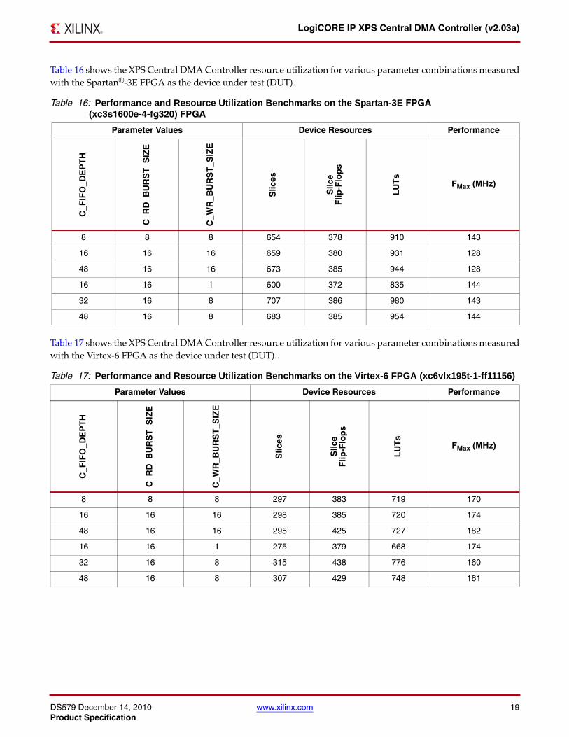
Table 16 shows the XPS Central DMA Controller resource utilization for various parameter combinations measuredwith the Spartan®-3E FPGA as the device under test (DUT).
Table 17 shows the XPS Central DMA Controller resource utilization for various parameter combinations measuredwith the Virtex-6 FPGA as the device under test (DUT)..
Table 16: Performance and Resource Utilization Benchmarks on the Spartan-3E FPGA (xc3s1600e-4-fg320) FPGA
Parameter Values Device Resources Performance
C_F
IFO
_DE
PT
H
C_R
D_B
UR
ST
_SIZ
E
C_W
R_B
UR
ST
_SIZ
E
Slic
es
Slic
e F
lip-F
lop
s
LU
Ts
FMax (MHz)
8 8 8 654 378 910 143
16 16 16 659 380 931 128
48 16 16 673 385 944 128
16 16 1 600 372 835 144
32 16 8 707 386 980 143
48 16 8 683 385 954 144
Table 17: Performance and Resource Utilization Benchmarks on the Virtex-6 FPGA (xc6vlx195t-1-ff11156)Parameter Values Device Resources Performance
C_F
IFO
_DE
PT
H
C_R
D_B
UR
ST
_SIZ
E
C_W
R_B
UR
ST
_SIZ
E
Slic
es
Slic
e F
lip-F
lop
s
LU
Ts
FMax (MHz)
8 8 8 297 383 719 170
16 16 16 298 385 720 174
48 16 16 295 425 727 182
16 16 1 275 379 668 174
32 16 8 315 438 776 160
48 16 8 307 429 748 161

DS579 December 14, 2010 www.xilinx.com 20Product Specification
LogiCORE IP XPS Central DMA Controller (v2.03a)
Table 18 shows the XPS Central DMA Controller resource utilization for various parameter combinations measuredwith Spartan-6 FPGA as the device under test (DUT).
System Performance
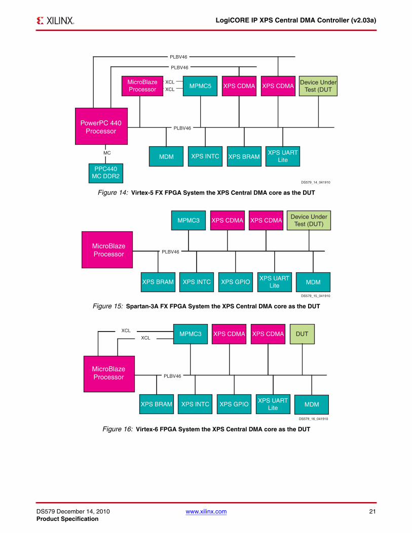
To measure the system performance (FMAX) of this core, this core was added the Device Under Test (DUT) to aVirtex-4 FPGA system as shown in Figure 13, a Virtex-5 FPGA system as shown in Figure 14, a Spartan-3A FPGAsystem as shown in Figure 15, a Spartan-6 FPGA system as shown in Figure 16, and a Virtex-6 FPGA system asshown in Figure 17 as.
Because the XPS Central DMA core will be used with other design modules in the FPGA, the utilization and timingnumbers reported in this section are estimates only. When the XPS Central DMA core is combined with otherdesigns in the system, the utilization of FPGA resources and timing of the XPS Central DMA design will vary fromthe results reported here.
Table 18: Performance and Resource Utilization Benchmarks on the Spartan-6 FPGA (xc6slx45-2-fgg484)
Parameter Values Device Resources Performance
C_F
IFO
_DE
PT
H
C_R
D_B
UR
ST
_SIZ
E
C_W
R_B
UR
ST
_SIZ
E
Slic
es
Slic
e F
lip-F
lop
s
LU
Ts
FMax (MHz)
8 8 8 289 564 727 101
16 16 16 299 566 730 100
48 16 16 305 577 720 110
16 16 1 290 553 660 111
32 16 8 315 616 766 112
48 16 8 310 590 737 115
X-Ref Target - Figure 13
Figure 13: Virtex-4 FX FPGA System the XPS Central DMA core as the DUT
PowerPC 405 Processor
MPMC5 XPS CDMADevice Under
Test (DUT)
XPS UARTLite
XPS GPIOXPS INTCXPS BRAM
DPLB1IPLB1
DPLB0
IPLB0
XPS CDMAPLBV46
PLBV46
PLBV46
DS579_13_041910
DS579 December 14, 2010 www.xilinx.com 21Product Specification
LogiCORE IP XPS Central DMA Controller (v2.03a)
X-Ref Target - Figure 14
Figure 14: Virtex-5 FX FPGA System the XPS Central DMA core as the DUT
X-Ref Target - Figure 15
Figure 15: Spartan-3A FX FPGA System the XPS Central DMA core as the DUT
X-Ref Target - Figure 16
Figure 16: Virtex-6 FPGA System the XPS Central DMA core as the DUT
MPMC5 XPS CDMADevice Under
Test (DUT
XPS UARTLite
XPS INTC
XPS CDMA
MDM
XCL
XCL
PLBV46
MicroBlaze
XPS BRAMMDM
PPC440MC DDR2
MC
PLBV46
PLBV46
PowerPC 440Processor
MicroBlazeProcessor
DS579_14_041910
MicroBlazeProcessor
MPMC3 XPS CDMA
XPS UARTLite
XPS GPIOXPS INTCXPS BRAM
XPS CDMA
MDM
PLBV46
DS579_15_041910
Device UnderTest (DUT)
MicroBlazeProcessor
MPMC3 XPS CDMA DUT
XPS UARTLite
XPS GPIOXPS INTCXPS BRAM
XPS CDMA
MDM
PLBV46
XCL
XCL
DS579_16_041910

DS579 December 14, 2010 www.xilinx.com 22Product Specification
LogiCORE IP XPS Central DMA Controller (v2.03a)
The target FPGA was then filled with logic to drive the LUT and BRAM utilization to approximately 70% and theI/O utilization to approximately 80%. Using the default tool options and the slowest speed grade for the targetFPGA, the resulting target FMAX numbers are shown in Table 19.
The target FMAX is influenced by the exact system and is provided for guidance. It is not a guaranteed value acrossall systems.
Specification ExceptionsN/A
SupportXilinx provides technical support for this LogiCORE product when used as described in the productdocumentation. Xilinx cannot guarantee timing, functionality, or support of product if implemented in devices thatare not defined in the documentation, if customized beyond that allowed in the product documentation, or ifchanges are made to any section of the design labeled DO NOT MODIFY.
X-Ref Target - Figure 17
Figure 17: Spartan-6 FPGA System the XPS Central DMA core as the DUT
Table 19: System Performance
Target FPGA Estimated FMAX (MHz)
S3A700 -4 90
V4FX60 -10 100
V5LXT50 -1 120
V6LX130t - 1 150
S6LX45t - 2 100
MicroBlazeProcessor
MPMC3 XPS CDMA DUT
XPS UARTLite
XPS GPIOXPS INTCXPS BRAM
XPS CDMA
MDM
PLBV46
DS579_17_041910

DS579 December 14, 2010 www.xilinx.com 23Product Specification
LogiCORE IP XPS Central DMA Controller (v2.03a)
Ordering InformationThis Xilinx LogiCORE IP module is provided at no additional cost with the Xilinx ISE Design Suite EmbeddedEdition software under the terms of the Xilinx End User License. The core is generated using the Xilinx ISEEmbedded Edition software (EDK).
Information about this and other Xilinx LogiCORE IP modules is available at the Xilinx Intellectual Property page.For information on pricing and availability of other Xilinx LogiCORE modules and software, please contact yourlocal Xilinx sales representative.
Reference DocumentsN/A
Revision HistoryThe following table shows the revision history for this document:
Notice of DisclaimerXilinx is providing this product documentation, hereinafter “Information,” to you “AS IS” with no warranty of any kind, expressor implied. Xilinx makes no representation that the Information, or any particular implementation thereof, is free from anyclaims of infringement. You are responsible for obtaining any rights you may require for any implementation based on theInformation. All specifications are subject to change without notice. XILINX EXPRESSLY DISCLAIMS ANY WARRANTYWHATSOEVER WITH RESPECT TO THE ADEQUACY OF THE INFORMATION OR ANY IMPLEMENTATION BASEDTHEREON, INCLUDING BUT NOT LIMITED TO ANY WARRANTIES OR REPRESENTATIONS THAT THISIMPLEMENTATION IS FREE FROM CLAIMS OF INFRINGEMENT AND ANY IMPLIED WARRANTIES OFMERCHANTABILITY OR FITNESS FOR A PARTICULAR PURPOSE. Except as stated herein, none of the Information may becopied, reproduced, distributed, republished, downloaded, displayed, posted, or transmitted in any form or by any meansincluding, but not limited to, electronic, mechanical, photocopying, recording, or otherwise, without the prior written consent ofXilinx.
Date Version Description of Revisions
10/30/07 1.0 Initial Xilinx release.
7/22/08 2.0 Added QPro Virtex-4 Hi-Rel and QPro Virtex-4 Rad Tolerant FPGA support.
12/22/08 3.0 Removed Virtex-2 Pro support and added Spartan-6 support.
4/24/09 3.1 Replaced references to supported device families and tool name(s) with hyperlink to PDF file.
4/19/10 3.2Updated to v2.01c for 12.1 release, converted to new DS template; updated Performance and Resource Utilization Benchmark tables for 12.1 release; added Spartan-6 and Virtex-6 details in XPS Central DMA System Performance Table.
7/23/10 3.3 Updated to v2.02.a for 12.2 release.
12/14/10 3.4 Updated to v2.03.a; incorporated CR567919.