Embed Size (px)
Citation preview
TriCore Debugger and Trace
TRACE32 Online Help
TRACE32 Directory
TRACE32 Index
TRACE32 Documents ......................................................................................................................
ICD In-Circuit Debugger ................................................................................................................
Processor Architecture Manuals ..............................................................................................
TriCore ......................................................................................................................................
TriCore Debugger and Trace ............................................................................................... 1
History ................................................................................................................................ 7
Brief Overview of Documents for New Users ................................................................. 7
Safety Precautions ............................................................................................................ 8
Introduction ....................................................................................................................... 9
Available Tools 9
Debugger 9
On-chip Trace 10
Serial Off-chip Trace (AGBT) 10
Parallel Off-chip Trace 10
Co-Processor Debugging (PCP/GTM) 10
Multicore Debugging and Tracing 10
Software Installation 11
Configuration 11
System Overview 11
Related Documents 12
Demo and Start-up Scripts 12
OCDS Levels 13
Debugging .......................................................................................................................... 14
Single-Core Debugging (AUDO) 15
Single-Core Debugging - Quick Start 15
Multicore Debugging (AURIX) 17
SMP Debugging - Quick Start 17
AMP Debugging - Quick Start 19
AMP vs. SMP 21
Selecting the right AURIX CPU 22
Understanding Multicore Startup by Application Code 22
About Ambiguous Symbols 23
Access Classes 24
TriCore Debugger and Trace 1 ©1989-2018 Lauterbach GmbH
Breakpoints 25
Software Breakpoints 25
On-chip Breakpoints 25
MAP.BOnchip Command 26
Advanced Breakpoints 26
Single Stepping 27
Assembler Level 27
HLL Level 27
Flash 28
Onchip Triggers (TrOnchip Window) 30
BenchMarkCounter 31
Example: Measuring Instructions and Stalls per Clock Cycle 31
Example: A-to-B Mode 33
Example: Record Counters Periodically 34
Watchpins 35
AUDO 35
AURIX 35
Cache Access 39
AURIX Devices 39
Parallel Usage of a 3rd-Party Tool 41
Physical Sharing of the Debug Port 41
Debugging an Application with the Memory Protection Unit Enabled 43
TriCore v1.6 and Later 43
TriCore v1.3.1 and Earlier 43
Debugging with MPU Enabled in RAM 43
Debugging with MPU Enabled in FLASH 44
Debugging through Resets and Power Cycles 45
Soft Resets 45
Hard Resets 46
Power Cycles 47
Internal Break Bus (JTAG) 49
Cerberus Access Protection 49
Troubleshooting 50
SYStem.Up Errors 50
Debugging Optimized Code 50
FAQ 52
Tracing ............................................................................................................................... 60
On-chip Trace (OCDS-L3) 60
Quick Start for Tracing with On-chip Trace (OCDS-L3) 60
Supported Features 61
Trace Control 62
Trace Evaluation 62
Impact of the Debugger on FPI Bus Tracing 62
TriCore Debugger and Trace 2 ©1989-2018 Lauterbach GmbH
Simple Trace Control 63
Examples 63
Command Reference ........................................................................................................ 67
Analyzer.Mode PCP Select PCP trace 67
About the BMC Commands 67
BMC.state Display BMC configuration window 67
BMC.CLOCK Provide core clock for cycle counter 69
BMC.<counter>.ATOB Control A-to-B mode 69
About the SYStem.CONFIG Commands 70
SYStem.CONFIG.state Display target configuration 70
SYStem.CONFIG Configure debugger according to target topology 71
Daisy-chain Example 73
TapStates 74
SYStem.CONFIG.CORE Assign core to TRACE32 instance 75
SYStem.CONFIG BreakPIN Define mapping of break pins 76
SYStem.CONFIG DAP Configure DAP interface 77
SYStem.CONFIG DAP.BreakPIN Define mapping of break pins 77
SYStem.CONFIG DAP.DAPENable Enable DAP mode on PORST 77
SYStem.CONFIG DAP.USERn Configure and set USER pins 78
SYStem.CONFIG.DEBUGPORT Select target interface 79
SYStem.CONFIG.DEBUGPORTTYPE Set debug cable interface mode 79
SYStem.CONFIG DXCPL Configure DXCPL 80
SYStem.CONFIG DXCPL.Timing Configure SPD timing for DXCPL 80
SYStem.CONFIG.EXTWDTDIS Disable external watchdog 80
SYStem.CONFIG PortSHaRing Control sharing of debug port with other tool 81
SYStem.CPU Select CPU 81
SYStem.CpuAccess Run-time CPU access (intrusive) 82
SYStem.JtagClock Set the JTAG frequency 82
SYStem.LOCK Tristate the JTAG port 83
SYStem.MemAccess Run-time memory access (non-intrusive) 84
SYStem.Mode Establish the communication with the CPU 85
SYStem.Option CPU specific commands 86
SYStem.Option BREAKFIX Enable workaround for asynchronous breaking 86
SYStem.Option CBSACCEN<x> Cerberus access protection 87
SYStem.Option DCFREEZE Do not invalidate cache 88
SYStem.Option DCREAD Read from data cache 88
SYStem.Option DOWNMODE Behavior of SYStem.Mode Down 89
SYStem.Option DUALPORT Run-time memory access for all windows 89
SYStem.Option DataTrace Enable data tracing 89
SYStem.Option ETK Debugging together with ETK from ETAS 90
SYStem.Option HeartBeat Bug fix to avoid FPI bus conflict 90
SYStem.Option ICFLUSH Flush instruction cache at 'Go' or 'Step' 91
SYStem.Option IMASKASM Disable interrupts while single stepping 91
TriCore Debugger and Trace 3 ©1989-2018 Lauterbach GmbH
SYStem.Option IMASKHLL Disable interrupts while HLL single stepping 91
SYStem.Option INTSTART Start address of interrupt routines 92
SYStem.Option INTUSE Number of implemented interrupts 92
SYStem.Option JTAGENSEQ Use JTAG initialization sequence 92
SYStem.Option KEYCODE Set debug interface password 93
SYStem.Option LBIST LBIST gap handling 93
SYStem.Option OCDSELOW Set OCDS line to low 94
SYStem.Option OVC Enable OVERLAY memory access 95
SYStem.Option PERSTOP Enable global peripheral suspend 95
SYStem.Option PMILBFIX Enable PMI line buffer invalidation workaround 95
SYStem.Option PostResetDELAY Delay after RESET is released 97
SYStem.Option ReadOnly Block all write accesses 97
SYStem.Option RESetBehavior Set behavior when a reset occurs 98
SYStem.Option ResetDetection Set how hard resets are detected 98
SYStem.Option RESetTMS State of TMS line at reset 99
SYStem.Option SOFTLONG Set 32 bit software breakpoints 99
SYStem.Option STEPONCHIP Step with onchip breakpoints 99
SYStem.Option STEPSOFT Step with software breakpoints 100
SYStem.Option TB1766FIX Bug fix for some TC1766 TriBoards 100
SYStem.Option TRAPSTART Start address of trap vectors 100
SYStem.Option WDTFIX Disables the watchdog on SYStem.Up 101
SYStem.Option WDTSUS Link the watchdog timer to the suspend bus 101
SYStem.RESetOut In-target reset 102
SYStem.state Open SYStem.state window 102
CPU specific TrOnchip Commands 103
TrOnchip.BreakBusN.BreakIN Configure break pin of 'BreakBus N' 103
TrOnchip.BreakBusN.BreakOUT Configure break pin of 'BreakBus N' 103
TrOnchip.BreakIN.<target> Connect break <target> to BreakBus 104
TrOnchip.BreakOUT.<source> Connect break <source> to BreakBus 104
<source> 105
HaLTEN 105
TrOnchip.CONVert Adjust range breakpoint in on-chip resource 106
TrOnchip.CountX Event X counter value 106
TrOnchip.CountY Event Y counter value 106
TrOnchip.EXTernal Configure TriCore break on BreakBus event 107
TrOnchip.RESet Reset settings for the on-chip trigger unit 107
TrOnchip.SoftWare Configure 'TriCore' break on debug instruction 107
TrOnchip.SusSWitch Enable or disable suspend switch 108
TrOnchip.SusSWitch.FORCE Force generation of suspend signal 108
TrOnchip.SusSWitch.Mode Set suspend switch mode 108
TrOnchip.SusTarget Connect special targets to the suspend bus 109
TrOnchip.SYNCHRONOUS Switches mode for data breakpoints 109
TrOnchip.TCompress Trace data compression 109
TriCore Debugger and Trace 4 ©1989-2018 Lauterbach GmbH
TrOnchip.TDelay Trace trigger delay (obsolete) 110
TrOnchip.TExtMode Mode for external trigger input 110
TrOnchip.TExtPol Polarity of external trigger input 110
TrOnchip.TMode Trace mode (obsolete) 110
TrOnchip.TR0 Specify trigger event 0 111
TrOnchip.TR1 Specify trigger event 1 112
TrOnchip.state Show on-chip trigger window 112
TrOnchip.X Select trigger source X 113
TrOnchip.Y Select trigger source Y 113
Technical Data ................................................................................................................... 114
JTAG Connector 114
Trace Connector 116
AMP 40 Connector 116
ERF8 22-pin Power.org Connector 117
Samtec 60 Connector 117
Technical Data for Debugger 119
Operation Voltage 119
Mechanical Dimensions 119
Technical Data for Trace 120
Operation Frequency 120
Operation Voltage 120
Mechanical Dimensions 121
Support 123
Available Tools 123
Compilers 126
Target Operating Systems 127
3rd-Party Tool Integrations 127
Products 129
Product Information 129
Order Information 131
Appendix ............................................................................................................................ 133
Parallel Off-chip Trace - OCDS-L2 Flow Trace (Analyzer) 133
Overview 133
Quick Start for Tracing with OCDS-L2 Trace (Analyzer) 133
Supported Features 134
Version History 135
Timestamp Accuracy 135
Concurrent Usage of OCDS-L2 Off-chip Trace and OCDS-L3 On-chip Trace 136
Simple Trace Control 136
Trace Break Signals (OCDS-L2) 136
Trace Examples 137
Troubleshooting for OCDS-L2 Trace 139
No Data in Trace.List Visible 139
TriCore Debugger and Trace 5 ©1989-2018 Lauterbach GmbH
Error Diagnosis 139
Searching for Errors 140
Error Messages 141
TriCore Debugger and Trace 6 ©1989-2018 Lauterbach GmbH
TriCore Debugger and Trace
Version 22-Mar-2018
History
16-Jan-18 Updated description of SYStem.Mode Down and SYStem.CONFIG DEBUGPORTTYPE to describe changed behavior.
16-Jan-18 Added descriptions of the new commands SYStem.Option DOWNMODE and SYStem.Option CBSACCEN<x>. Revised section “Parallel Usage of a 3rd-Party Tool”.
Brief Overview of Documents for New Users
Architecture-independent information:
• “Debugger Basics - Training” (training_debugger.pdf): Get familiar with the basic features of a TRACE32 debugger.
• “T32Start” (app_t32start.pdf): T32Start assists you in starting TRACE32 PowerView instances for different configurations of the debugger. T32Start is only available for Windows.
• “General Commands” (general_ref_<x>.pdf): Alphabetic list of debug commands.
Architecture-specific information:
• “Processor Architecture Manuals”: These manuals describe commands that are specific for the processor architecture supported by your debug cable. To access the manual for your processor architecture, proceed as follows:
- Choose Help menu > Processor Architecture Manual.
• “RTOS Debuggers” (rtos_<x>.pdf): TRACE32 PowerView can be extended for operating system-aware debugging. The appropriate RTOS manual informs you how to enable the OS-aware debugging.
TriCore Debugger and Trace 7 ©1989-2018 Lauterbach GmbH
Safety Precautions
Caution: To prevent debugger and target from damage it is recommended to connect or disconnect the debug cable only while the target power is OFF.
Recommendation for the software start:• Disconnect the debug cable from the target while the target power
is off.• Connect the host system, the TRACE32 hardware and the debug
cable.• Power ON the TRACE32 hardware.• Start the TRACE32 software to load the debugger firmware.• Connect the debug cable to the target.• Switch the target power ON.• Configure your debugger e.g. via a start-up script.
Power down:• Switch off the target power.• Disconnect the debug cable from the target.• Close the TRACE32 software.• Power OFF the TRACE32 hardware.
TriCore Debugger and Trace 8 ©1989-2018 Lauterbach GmbH
Introduction
This document describes the processor specific settings and features for the TRACE32 TriCore debugger.
Please keep in mind that the Processor Architecture Manual (the document you are reading at the moment) describes all features TRACE32 provides especially for the TriCore architecture. The rest of the online help is generic for all chips supported by Lauterbach.
Available Tools
This chapter gives an overview of available Lauterbach tools for the TriCore architecture.
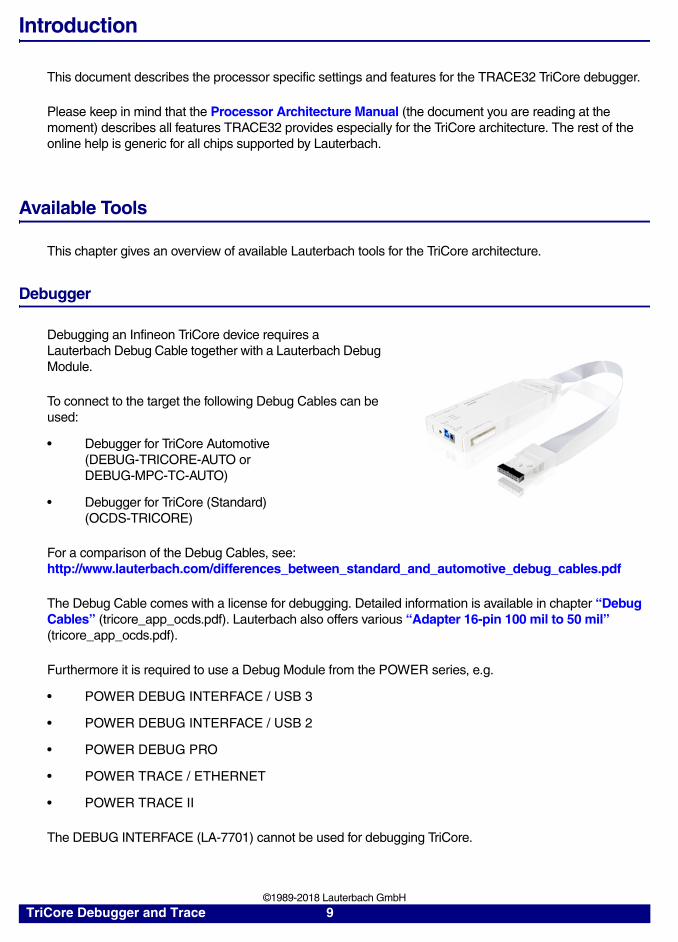
Debugger
Debugging an Infineon TriCore device requires a Lauterbach Debug Cable together with a Lauterbach Debug Module.
To connect to the target the following Debug Cables can be used:
• Debugger for TriCore Automotive (DEBUG-TRICORE-AUTO or DEBUG-MPC-TC-AUTO)
• Debugger for TriCore (Standard)(OCDS-TRICORE)
For a comparison of the Debug Cables, see:http://www.lauterbach.com/differences_between_standard_and_automotive_debug_cables.pdf
The Debug Cable comes with a license for debugging. Detailed information is available in chapter “Debug Cables” (tricore_app_ocds.pdf). Lauterbach also offers various “Adapter 16-pin 100 mil to 50 mil” (tricore_app_ocds.pdf).
Furthermore it is required to use a Debug Module from the POWER series, e.g.
• POWER DEBUG INTERFACE / USB 3
• POWER DEBUG INTERFACE / USB 2
• POWER DEBUG PRO
• POWER TRACE / ETHERNET
• POWER TRACE II
The DEBUG INTERFACE (LA-7701) cannot be used for debugging TriCore.
TriCore Debugger and Trace 9 ©1989-2018 Lauterbach GmbH
On-chip Trace
On-chip tracing requires no extra Lauterbach hardware, it can be configured and read out with a regular Debugger. The trace related features are enables with the Trace License for TriCore ED (TriCore-MCDS). Note that only TriCore Emulation Devices (ED) provide an onchip trace buffer.
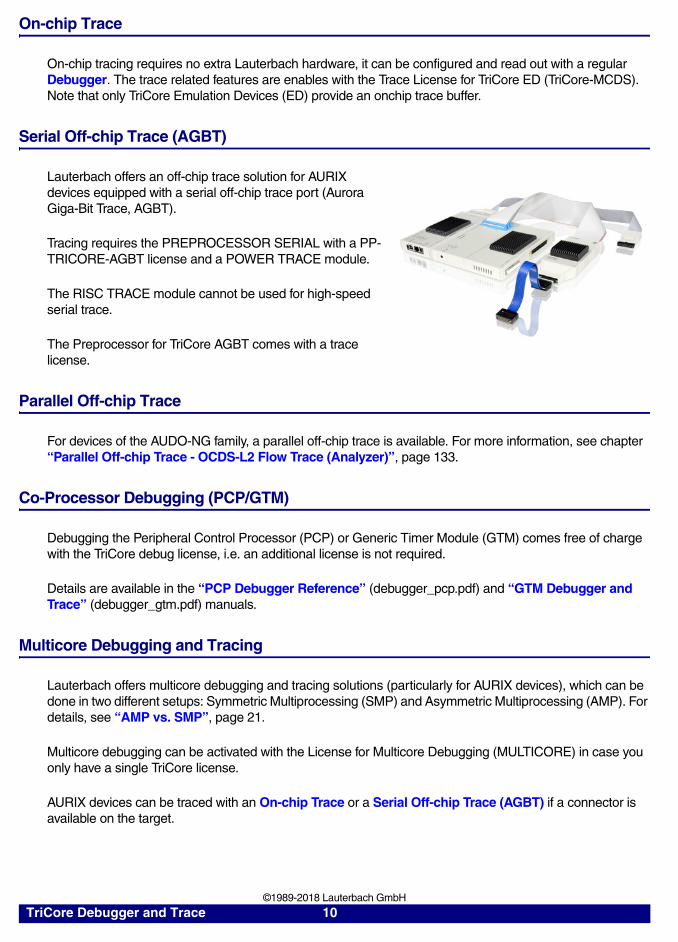
Serial Off-chip Trace (AGBT)
Lauterbach offers an off-chip trace solution for AURIX devices equipped with a serial off-chip trace port (Aurora Giga-Bit Trace, AGBT).
Tracing requires the PREPROCESSOR SERIAL with a PP-TRICORE-AGBT license and a POWER TRACE module.
The RISC TRACE module cannot be used for high-speed serial trace.
The Preprocessor for TriCore AGBT comes with a trace license.
Parallel Off-chip Trace
For devices of the AUDO-NG family, a parallel off-chip trace is available. For more information, see chapter “Parallel Off-chip Trace - OCDS-L2 Flow Trace (Analyzer)”, page 133.
Co-Processor Debugging (PCP/GTM)
Debugging the Peripheral Control Processor (PCP) or Generic Timer Module (GTM) comes free of charge with the TriCore debug license, i.e. an additional license is not required.
Details are available in the “PCP Debugger Reference” (debugger_pcp.pdf) and “GTM Debugger and Trace” (debugger_gtm.pdf) manuals.
Multicore Debugging and Tracing
Lauterbach offers multicore debugging and tracing solutions (particularly for AURIX devices), which can be done in two different setups: Symmetric Multiprocessing (SMP) and Asymmetric Multiprocessing (AMP). For details, see “AMP vs. SMP”, page 21.
Multicore debugging can be activated with the License for Multicore Debugging (MULTICORE) in case you only have a single TriCore license.
AURIX devices can be traced with an On-chip Trace or a Serial Off-chip Trace (AGBT) if a connector is available on the target.
TriCore Debugger and Trace 10 ©1989-2018 Lauterbach GmbH
Software Installation
Please follow chapter “Software Installation” (icd_quick_installation.pdf) on how to install the TRACE32 software:
• An installer is available for a complete TRACE32 installation under Windows. See “MS Windows” in ICD Quick Installation, page 24 (icd_quick_installation.pdf).
• For a complete installation of TRACE32 under Linux, see “PC_LINUX” in ICD Quick Installation, page 27 (icd_quick_installation.pdf).
Configuration
System Overview
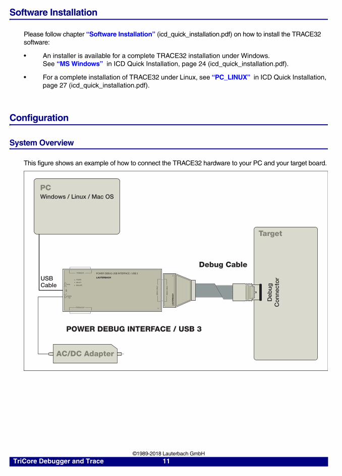
This figure shows an example of how to connect the TRACE32 hardware to your PC and your target board.
Target
DE
BU
G C
AB
LE
LA
UT
ER
BA
CH
Debug Cable
POWER DEBUG INTERFACE / USB 3
AC/DC Adapter
PC
USBCable
LAUTERBACHPOWER
SELECT
EMULATE
PODBUS OUT
US
B
PODBUS IN
DE
BU
G C
AB
LE
POWER7-9V
TRIG
POWER DEBUG USB INTERFACE / USB 3D
ebug
Co
nnec
tor
Windows / Linux / Mac OS
TriCore Debugger and Trace 11 ©1989-2018 Lauterbach GmbH
Related Documents
• “Onchip/NOR FLASH Programming User’s Guide” (norflash.pdf): Onchip FLASH and off-chip NOR FLASH programming.
• “Application Note Debug Cable TriCore” (tricore_app_ocds.pdf): All about the TriCore debug cables and available accessories.
• “Debugger Basics - SMP Training” (training_debugger_smp.pdf): SMP debugging.
• “AURIX Trace Training” (training_aurix_trace.pdf): Training for AURIX devices.
• “MCDS User’s Guide” (mcds_user.pdf): Basic and advanced information on the MCDS and the Infineon Emulation Devices.
• “PCP Debugger Reference” (debugger_pcp.pdf): Debugging and tracing the Peripheral Control Processor (PCP).
• “GTM Debugger and Trace” (debugger_gtm.pdf): Debugging and tracing the Generic Timer Module (GTM).
Demo and Start-up Scripts
Lauterbach provides ready-to-run start-up scripts for all TriCore chips. Choose File menu > Search for Script.
In your TRACE32 installation directory there is a subdirectory ~~/demo/tricore/ where you will find example scripts and demo software. The subdirectory ~~/demo/tricore/ includes:
hardware/ Ready-to-run debugging and flash programming demos for evaluation boards (e.g. Infineon TriBoard).
Recommended for getting started!
flash/ Binaries for target based programming and example declarations for internal flash.
etc/ Various examples, e.g. data trace, terminal application, PCP debugging, MCDS, …
kernel/ Various RTOS examples.
compiler/ Compiler examples.
fdx/ Example applications for the FDX feature.
TriCore Debugger and Trace 12 ©1989-2018 Lauterbach GmbH
OCDS Levels
OCDS (On-chip Debug Solution) is the on-chip logic that implements the debug, trace and calibration functionality. Infineon defines three OCDS levels:
• OCDS-L1 refers to the basic debug functionality (execution control, register and memory access). The 16-pin JTAG connector is often called OCDS-L1 connector.
• OCDS-L2 refers to the (deprecated) parallel off-chip trace. The 40-pin AMP connector and the 60-pin SAMTEC connector for the parallel trace is called OCDS-L2 connector.
• OCDS-L3 is the trace, trigger and calibration functionality in the MCDS. Although defined by Infineon the term is rarely used. Instead the term MCDS is used. MCDS is accessed by the debugger via the debug port (JTAG or DAP), the connector for the AGBT high-speed serial trace is called AGBT connector.
Today the differentiation between the OCDS levels is not very common any more. OCDS refers to the debugging features and MCDS to the trace- and calibration features. Calibration is not supported by TRACE32, but TRACE32 cooperates with third-party tools performing calibration.
TriCore Debugger and Trace 13 ©1989-2018 Lauterbach GmbH
Debugging
Debugging, as described in this chapter, includes:
• Core debugging (run control, breakpoints)
• Memory and register access
• Trace configuration
• Additional debug features (performance counter, run-time memory access, …)
It is performed via classic JTAG or alternatively via DAP.
This chapter covers the following topics:
• “Single-Core Debugging (AUDO)”, page 15
• “Multicore Debugging (AURIX)”, page 17
• “Access Classes”, page 24
• “Flash”, page 28
• “Onchip Triggers (TrOnchip Window)”, page 30
• “Internal Break Bus (JTAG)”, page 49
• “Suspend Switch”, page 49
• “Assembler and Disassembler Options”, page 40
• “Parallel Usage of a 3rd-Party Tool”, page 41
• “Internal Break Bus (JTAG)”, page 49
• “Troubleshooting”, page 50
• “FAQ”, page 52
TriCore Debugger and Trace 14 ©1989-2018 Lauterbach GmbH
Single-Core Debugging (AUDO)
This chapter introduces a typical start-up sequence for single-core debugging. Depending on your application not all steps might be necessary. The example shown uses a TC1766 B-Step on an Infineon TriBoard-TC1766.
For other chips and more examples, see the chapter Demo and Start-up Scripts.
Single-Core Debugging - Quick Start
1. Prepare the start.
- Connect the Debug Cable to your target. Check the orientation of the connector. Pin 1 of the Debug Cable is marked with a small triangle next to the nose of the target connector.
- Power up your TRACE32 system.
- Start the TRACE32 Debugger Software for TriCore.
- Power up your target.
2. Inform TRACE32 which chip you want to debug.
3. Establish the communication between the debugger and your target chip.
This command resets the chip and enters debug mode. After this command is executed it is possible to access memory and registers.
4. Load your application program.
The sub-command of the Data.LOAD command (here, Elf) depends on the file format generated by the compiler. For information on the compiler sub-commands, refer to section Compiler. A detailed description of the Data.LOAD command is given in “General Commands Reference”.
If your application runs from FLASH, FLASH programming has to be enabled before the Data.LOAD command is used. Scripts that enable FLASH programing can be found in ~~/demo/tricore/flash.
To prevent damage please take care to follow this sequence all the time you are preparing a start.
SYStem.CPU TC1766
SYStem.Up
Data.LOAD.Elf myprog.elf
TriCore Debugger and Trace 15 ©1989-2018 Lauterbach GmbH
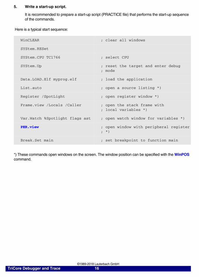
5. Write a start-up script.
It is recommended to prepare a start-up script (PRACTICE file) that performs the start-up sequence of the commands.
Here is a typical start sequence:
*) These commands open windows on the screen. The window position can be specified with the WinPOS command.
WinCLEAR ; clear all windows
SYStem.RESet
SYStem.CPU TC1766 ; select CPU
SYStem.Up ; reset the target and enter debug; mode
Data.LOAD.Elf myprog.elf ; load the application
List.auto ; open a source listing *)
Register /SpotLight ; open register window *)
Frame.view /Locals /Caller ; open the stack frame with ; local variables *)
Var.Watch %Spotlight flags ast ; open watch window for variables *)
PER.view ; open window with peripheral register; *)
Break.Set main ; set breakpoint to function main
TriCore Debugger and Trace 16 ©1989-2018 Lauterbach GmbH
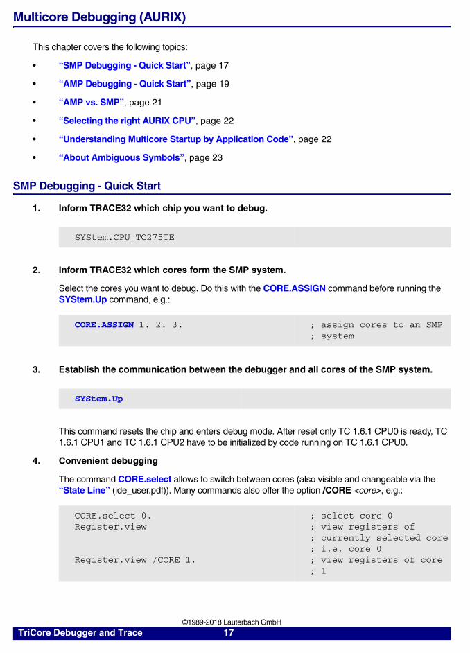
Multicore Debugging (AURIX)
This chapter covers the following topics:
• “SMP Debugging - Quick Start”, page 17
• “AMP Debugging - Quick Start”, page 19
• “AMP vs. SMP”, page 21
• “Selecting the right AURIX CPU”, page 22
• “Understanding Multicore Startup by Application Code”, page 22
• “About Ambiguous Symbols”, page 23
SMP Debugging - Quick Start
1. Inform TRACE32 which chip you want to debug.
2. Inform TRACE32 which cores form the SMP system.
Select the cores you want to debug. Do this with the CORE.ASSIGN command before running the SYStem.Up command, e.g.:
3. Establish the communication between the debugger and all cores of the SMP system.
This command resets the chip and enters debug mode. After reset only TC 1.6.1 CPU0 is ready, TC 1.6.1 CPU1 and TC 1.6.1 CPU2 have to be initialized by code running on TC 1.6.1 CPU0.
4. Convenient debugging
The command CORE.select allows to switch between cores (also visible and changeable via the “State Line” (ide_user.pdf)). Many commands also offer the option /CORE <core>, e.g.:
SYStem.CPU TC275TE
CORE.ASSIGN 1. 2. 3. ; assign cores to an SMP ; system
SYStem.Up
CORE.select 0.Register.view
Register.view /CORE 1.
; select core 0; view registers of; currently selected core; i.e. core 0; view registers of core; 1
TriCore Debugger and Trace 17 ©1989-2018 Lauterbach GmbH

5. Summary
Refer to the SMP demo scripts for details, e.g.:
The above script above can be found in ~~/demo/tricore/hardware/triboard-tc2x5/tc275te.
Copy the demo script and adjust it to your needs to get started with your own application in SMP mode.
PSTEP tc275te_smp_demo_multisieve.cmm
TriCore Debugger and Trace 18 ©1989-2018 Lauterbach GmbH
AMP Debugging - Quick Start
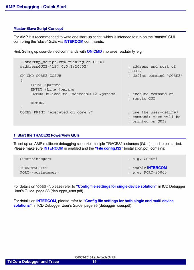
Master-Slave Script Concept
For AMP it is recommended to write one start-up script, which is intended to run on the “master” GUI controlling the “slave” GUIs via INTERCOM commands.
Hint: Setting up user-defined commands with ON CMD improves readability, e.g.:
1. Start the TRACE32 PowerView GUIs
To set up an AMP multicore debugging scenario, multiple TRACE32 instances (GUIs) need to be started. Please make sure INTERCOM is enabled and the “File config.t32” (installation.pdf) contains:
For details on “CORE=”, please refer to “Config file settings for single device solution” in ICD Debugger User’s Guide, page 33 (debugger_user.pdf).
For details on INTERCOM, please refer to “Config file settings for both single and multi device solutions” in ICD Debugger User’s Guide, page 35 (debugger_user.pdf).
; startup_script.cmm running on GUI0:&addressGUI2="127.0.0.1:20002"
ON CMD CORE2 GOSUB(
LOCAL ¶msENTRY %Line ¶msINTERCOM.execute &addressGUI2 ¶ms
RETURN)CORE2 PRINT "executed on core 2"
; address and port of; GUI2; define command “CORE2”
; execute command on; remote GUI
; use the user-defined; command: text will be; printed on GUI2
CORE=<integer>
IC=NETASSISTPORT=<portnumber>
; e.g. CORE=1
; enable INTERCOM; e.g. PORT=20000
TriCore Debugger and Trace 19 ©1989-2018 Lauterbach GmbH
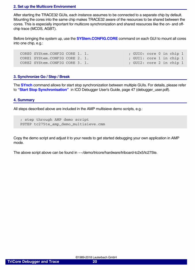
2. Set up the Multicore Environment
After starting the TRACE32 GUIs, each instance assumes to be connected to a separate chip by default. Mounting the cores into the same chip makes TRACE32 aware of the resources to be shared between the cores. This is especially important for multicore synchronization and shared resources like the on- and off-chip trace (MCDS, AGBT).
Before bringing the system up, use the SYStem.CONFIG.CORE command on each GUI to mount all cores into one chip, e.g.:
3. Synchronize Go / Step / Break
The SYnch command allows for start stop synchronization between multiple GUIs. For details, please refer to “Start Stop Synchronisation” in ICD Debugger User’s Guide, page 47 (debugger_user.pdf).
4. Summary
All steps described above are included in the AMP multisieve demo scripts, e.g.:
Copy the demo script and adjust it to your needs to get started debugging your own application in AMP mode.
The above script above can be found in ~~/demo/tricore/hardware/triboard-tc2x5/tc275te.
CORE0 SYStem.CONFIG CORE 1. 1.CORE1 SYStem.CONFIG CORE 2. 1.CORE2 SYStem.CONFIG CORE 3. 1.
; GUIO: core 0 in chip 1; GUI1: core 1 in chip 1; GUI2: core 2 in chip 1
; step through AMP demo scriptPSTEP tc275te_amp_demo_multisieve.cmm
TriCore Debugger and Trace 20 ©1989-2018 Lauterbach GmbH
AMP vs. SMP
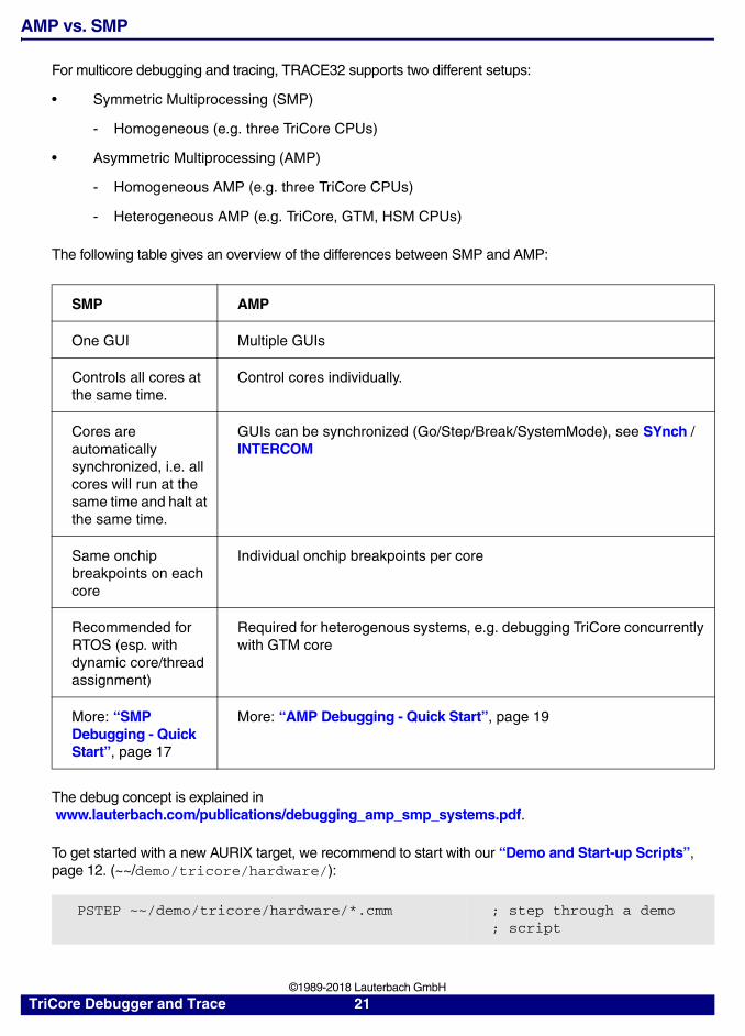
For multicore debugging and tracing, TRACE32 supports two different setups:
• Symmetric Multiprocessing (SMP)
- Homogeneous (e.g. three TriCore CPUs)
• Asymmetric Multiprocessing (AMP)
- Homogeneous AMP (e.g. three TriCore CPUs)
- Heterogeneous AMP (e.g. TriCore, GTM, HSM CPUs)
The following table gives an overview of the differences between SMP and AMP:
The debug concept is explained in www.lauterbach.com/publications/debugging_amp_smp_systems.pdf.
To get started with a new AURIX target, we recommend to start with our “Demo and Start-up Scripts”, page 12. (~~/demo/tricore/hardware/):
SMP AMP
One GUI Multiple GUIs
Controls all cores at the same time.
Control cores individually.
Cores are automatically synchronized, i.e. all cores will run at the same time and halt at the same time.
GUIs can be synchronized (Go/Step/Break/SystemMode), see SYnch / INTERCOM
Same onchip breakpoints on each core
Individual onchip breakpoints per core
Recommended for RTOS (esp. with dynamic core/thread assignment)
Required for heterogenous systems, e.g. debugging TriCore concurrently with GTM core
More: “SMP Debugging - Quick Start”, page 17
More: “AMP Debugging - Quick Start”, page 19
PSTEP ~~/demo/tricore/hardware/*.cmm ; step through a demo; script
TriCore Debugger and Trace 21 ©1989-2018 Lauterbach GmbH
Selecting the right AURIX CPU
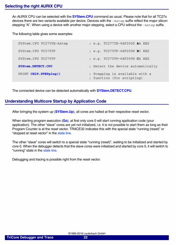
An AURIX CPU can be selected with the SYStem.CPU command as usual. Please note that for all TC27x devices there are two variants available per device. Devices with the -Astep suffix reflect the major silicon stepping “A”. When using a device with another major stepping, select a CPU without the -Astep suffix.
The following table gives some examples:
The connected device can be detected automatically with SYStem.DETECT.CPU.
Understanding Multicore Startup by Application Code
After bringing the system up (SYStem.Up), all cores are halted at their respective reset vector.
When starting program execution (Go), at first only core 0 will start running application code (your application). The other “slave” cores are yet not initialized, i.e. it is not possible to start them as long as their Program Counter is at the reset vector. TRACE32 indicates this with the special state “running (reset)” or “stopped at reset vector” in the state line.
The other “slave” cores will switch to a special state “running (reset)”, waiting to be initialized and started by core 0. When the debugger detects that the slave cores were initialized and started by core 0, it will switch to “running” state in the state line.
Debugging and tracing is possible right from the reset vector.
SYStem.CPU TC275TE-Astep ; e.g. TC277TE-64F200S AA EES
SYStem.CPU TC275TF ; e.g. TC275TF-64F200W BC EES
SYStem.CPU TC275TP ; e.g. TC275TP-64F200W CA EES
SYStem.DETECT.CPU ; Detect the device automatically
PRINT CHIP.STEPping() ; Stepping is available with a; function (for scripting)
TriCore Debugger and Trace 22 ©1989-2018 Lauterbach GmbH
About Ambiguous Symbols
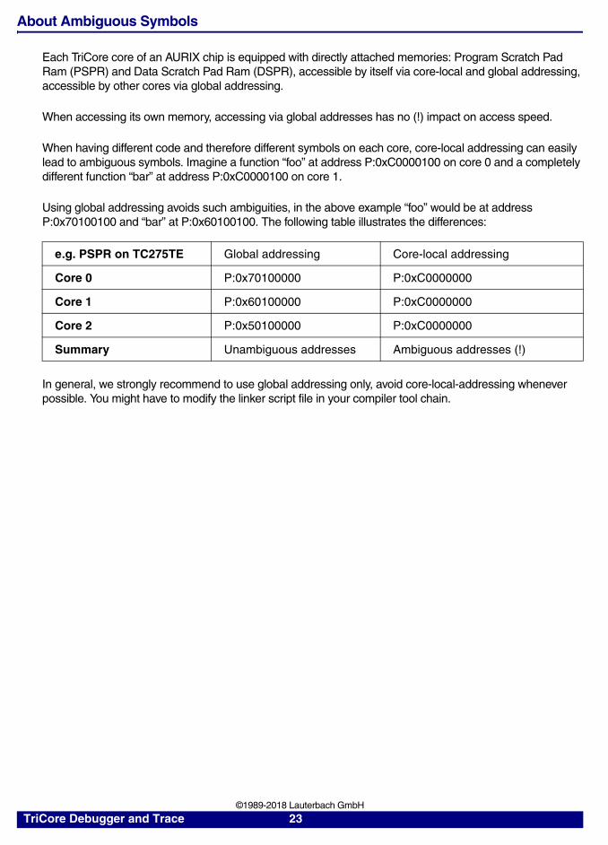
Each TriCore core of an AURIX chip is equipped with directly attached memories: Program Scratch Pad Ram (PSPR) and Data Scratch Pad Ram (DSPR), accessible by itself via core-local and global addressing, accessible by other cores via global addressing.
When accessing its own memory, accessing via global addresses has no (!) impact on access speed.
When having different code and therefore different symbols on each core, core-local addressing can easily lead to ambiguous symbols. Imagine a function “foo” at address P:0xC0000100 on core 0 and a completely different function “bar” at address P:0xC0000100 on core 1.
Using global addressing avoids such ambiguities, in the above example “foo” would be at address P:0x70100100 and “bar” at P:0x60100100. The following table illustrates the differences:
In general, we strongly recommend to use global addressing only, avoid core-local-addressing whenever possible. You might have to modify the linker script file in your compiler tool chain.
e.g. PSPR on TC275TE Global addressing Core-local addressing
Core 0 P:0x70100000 P:0xC0000000
Core 1 P:0x60100000 P:0xC0000000
Core 2 P:0x50100000 P:0xC0000000
Summary Unambiguous addresses Ambiguous addresses (!)
TriCore Debugger and Trace 23 ©1989-2018 Lauterbach GmbH

Access Classes
For background information about the term access class, see “TRACE32 Glossary” (glossary.pdf).
For TriCore, the following memory access classes are available:
P: and D: display the same memory, the difference is in handling the symbols.
Prepending an E as attribute to the memory class will make memory accesses possible even when the CPU is running. See SYStem.MemAccess and SYStem.CpuAccess for more information.
SYStem.Option DUALPORT will enable the runtime update of almost all windows so memory class attribute E is not necessary. Although the core is not stopped for accessing the memory this can slow down program execution since the CPU and debugger both access the on-chip buses.
With SYStem.Option DCREAD ON all data memory accesses (D:) will be redirected cached data memory accesses (DC:).
Memory Access Class
Description
P Program (memory as seen by CPU’s instruction fetch)
D Data
EEC Emulation Memory on EECOnly available on TriCore Emulation Devices for accessing the Emulation Extension Chip.
IC Instruction Cache
DC Data Cache (memory as seen by CPU’s data access)
NC No Cache (access with caching inhibited)
TriCore Debugger and Trace 24 ©1989-2018 Lauterbach GmbH
Breakpoints
TRACE32 uses two techniques to implement breakpoints: Software breakpoints and on-chip breakpoints.
Software Breakpoints
Software breakpoints are only available for program breakpoints. If a program breakpoint is set to an instruction, the original instruction at the breakpoint location is patched by a break code. This patching is the reason why software breakpoints are usually only used in RAM areas.
Software breakpoints in FLASH memory are also supported (see FLASH.AUTO in “General Commands Reference Guide F” (general_ref_f.pdf), chapter FLASH), but their use is not recommended since they drastically reduce the FLASH’s lifetime.
On-chip Breakpoints
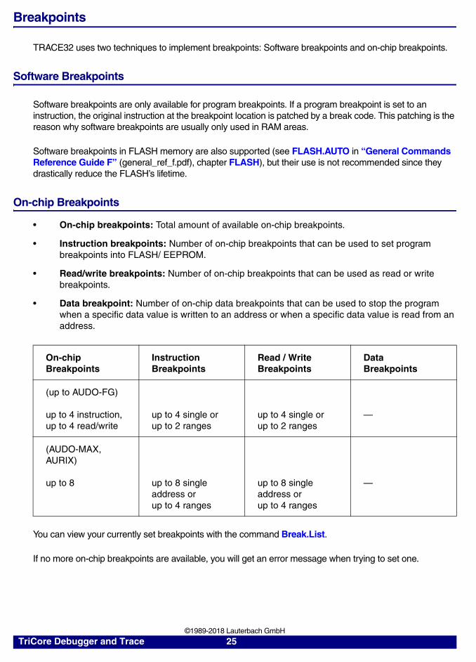
• On-chip breakpoints: Total amount of available on-chip breakpoints.
• Instruction breakpoints: Number of on-chip breakpoints that can be used to set program breakpoints into FLASH/ EEPROM.
• Read/write breakpoints: Number of on-chip breakpoints that can be used as read or write breakpoints.
• Data breakpoint: Number of on-chip data breakpoints that can be used to stop the program when a specific data value is written to an address or when a specific data value is read from an address.
You can view your currently set breakpoints with the command Break.List.
If no more on-chip breakpoints are available, you will get an error message when trying to set one.
On-chipBreakpoints
InstructionBreakpoints
Read / WriteBreakpoints
DataBreakpoints
(up to AUDO-FG)
up to 4 instruction,up to 4 read/write
up to 4 single orup to 2 ranges
up to 4 single orup to 2 ranges
—
(AUDO-MAX, AURIX)
up to 8 up to 8 single address orup to 4 ranges
up to 8 single address orup to 4 ranges
—
TriCore Debugger and Trace 25 ©1989-2018 Lauterbach GmbH
Intrusive Breakpoints
TRACE32 PowerView uses so-called intrusive breakpoint to implement a breakpoint, if the core in use does not provide the means to set a complex breakpoint.
MAP.BOnchip Command
Previously it was necessary to inform the debugger about the location of read-only memory on the target. This allows the debugger to automatically use on-chip breakpoints. Meanwhile, the debugger automatically sets Onchip breakpoints when read-only memory is detected. Today the command MAP.BOnchip <address_range> is rarely used.
Advanced Breakpoints
When using an Infineon Emulation Device, the MCDS part of the Emulation Extension Chip allows to set advanced breakpoints. Please refer to the “MCDS Breakpoints” in MCDS User’s Guide, page 25 (mcds_user.pdf) for details.
; stop the program execution at the 1000. call of the function sieveBreak.Set sieve /Program /COUNT 1000.
; stop the program execution if the byte 0x0 is written ; to the variable flags[3]Var.Break.Set flags[3] /Write /DATA.Byte 0x0
Note Only one intrusive breakpoints can be set on read/write breakpoints.
TriCore Debugger and Trace 26 ©1989-2018 Lauterbach GmbH
Single Stepping
OCDS does not offer a single-stepping feature so this has to be emulated by the debugger. We differentiate between single-stepping on assembler level and single-stepping on HLL level.
Assembler Level
For single-stepping on assembler level, use the Step.Asm command. An assembler level single-step is performed by default in mixed or assembler mode.Use SYStem.Option IMASKASM to control whether interrupts should be enabled during single-stepping.
On-chip Breakpoint Ranges (Default)
By default, the TriCore uses on-chip breakpoint ranges for implementing single-stepping. This allows the detection of exceptions (interrupts, traps) or any abnormal program execution.
SYStem.Option STEPSOFT and SYStem.Option STEPONCHIP both have to be disabled (OFF) for activating the default behavior.
Software Breakpoints
With SYStem.Option STEPSOFT one or two software breakpoint instructions are used for single-stepping. This is required when the Memory Protection Unit shall be used for memory protection. Note that software breakpoints can also be used in FLASH memory. A special setup is required for this to work.
As side effect, the interrupt handler may run silently in the background without the user noticing. So data required for the current function may change while stepping, thus resulting in a different behavior.
On-chip Breakpoint
With SYStem.Option STEPONCHIP an on-chip breakpoint with Break-After-Make is used for single-stepping.
This is mainly used as a workaround for a silicon bug (CPU_TC.115) which prevents a proper suspend of an already taken interrupt. As a result, the interrupt handler will run silently in the background without the user noticing. So data required for the current function may change while stepping, thus resulting in a different behavior.
In case SYStem.Option STEPSOFT is enabled at the same time, SYStem.Option STEPONCHIP will have no effect.
HLL Level
For single-stepping on HLL level, use the Step.Hll command. An HLL level single-step is performed by default in HLL mode.
Use SYStem.Option IMASKHLL to control whether interrupts should be enabled during single-stepping.
There are no options to configure the behavior, the debugger will always choose the correct implementation depending on the kind of memory.
TriCore Debugger and Trace 27 ©1989-2018 Lauterbach GmbH
Flash
Programming the flash memory is explained in detail in chapter “FLASH” (general_ref_f.pdf). This chapter will only give a short overview.
TriCore devices can be efficiently programmed with target controlled flash algorithms. They require a flash declaration, which can be found in the ~~/demo/tricore/flash/directory of the TRACE32 installation.
After the flash is declared, TRACE32 offers three approaches:
• FLASH.Erase and FLASH.Program
• FLASH.Auto
• FLASH.ReProgram (recommended)
For a lineup, see “TriCore On-Chip FLASH Programming” (tricore_app_flash.pdf).
Flashing an application typically follows these steps:
1. Prepare flash programming (declarations)
- Using FLASH.Create commands
- Or using provided scripts in ~~/demo/tricore/flash/
2. Enable flash programming using FLASH.ReProgram ALL.
3. Load an application usingData.LOAD <file>.
4. Finally program the flash using FLASH.ReProgram off.
All these steps, including device-specific declarations, are provided in the flash demo scripts. Use
for a comprehensive step-by-step procedure.
PSTEP ~~/demo/tricore/flash/tc*.cmm ; run flash script
TriCore Debugger and Trace 28 ©1989-2018 Lauterbach GmbH
Flashing and Debugging AURIX Devices
General help for flashing is available in chapter “FLASH” in General Commands Reference Guide F, page 39 (general_ref_f.pdf).
The onchip flash on AURIX devices has three states: 0, 1 and Bus Error.
By default, an erased flash sector returns a Bus Error on read access, indicated as “????????” in a Data.dump window. It is caused by an ECC error in the chip, which can be changed with the FLASH0_MARP.TRAPDIS and FLASH0_MARD.TRAPDIS register fields.
If you prefer to have an erased flash set to zero, simply run Data.Set <range> %Long 0x0 before loading your application, e.g.:
To make sure that another core is not intervening while flashing, it is recommended to switch to single-core debugging before flashing an application. All required steps are demonstrated in the flash script, e.g. in ~~/demo/tricore/flash/tc27x.cmm:
AURIX devices have several security features. Be careful not to lock yourself out when flashing a device!
• Boot Mode Headers (BMHD):
Do not reboot or unpower your device in case all BMHD (Boot Mode Headers) do not contain valid information. This is normally the case after having erased the internal program flash or loading an object or binary file without a valid BMHD.
• Hardware Security Module (HSM):
Do not enable HSM boot when no valid HSM code is present. This will lock your device permanently. See also “Flashing the Hardware Security Module (HSM)”, page 30.
• User Configuration Blocks (UCB):
Pay special attention when modifying the UCB. An invalid or erroneous content will lock your device permanently. This also happens in case the confirmation code is neither “unlocked” nor “confirmed”.
FLASH.ReProgram 0xA0080000-- 0xA009FFFF /Erase
; Activate flash region; for programming
Data.Set 0xA0080000--0xA009FFFF %Long 0x0 ; set to zero
Data.LOAD.Elf myapp.elf ; load ELF file
FLASH.ReProgram off ; Erase and program; modified region
DO ~~/demo/tricore/flash/tc2*.cmm ; run flash script
TriCore Debugger and Trace 29 ©1989-2018 Lauterbach GmbH
After flashing the application, a multicore debug scenario can be started as usual.
Hint: Use the option /NoCODE of the Data.LOAD command to load only the symbols (without downloading code), e.g.:
Flashing the Hardware Security Module (HSM)
When flashing the HSM, use the same precautions as described in “Flashing and Debugging AURIX Devices”, page 29.
The HSM can be flashed with the scripts ~~/demo/tricore/flash/tc2*-hsm.cmm: ,
Onchip Triggers (TrOnchip Window)
Onchip triggers can be influenced with the TrOnchip.view window. It affects primarily “On-chip Breakpoints”, page 25, and allows to control the Multi-Core Break Switch (MCBS) providing two internal Break Buses and a Suspend Switch.
See the TrOnchip commands for more information.
Data.LOAD.elf my_application.elf /NoCODE ; Load just the symbolic; information of an al-; ready flashed appli- ; cation
DO ~~/demo/tricore/flash/tc2*-hsm.cmm ; run flash script
Do not enable HSM boot when no valid HSM code is present. This will lock your device permanently. See the Infineon documentation and contact your Infineon FAE for more information on HSM.
TriCore Debugger and Trace 30 ©1989-2018 Lauterbach GmbH
BenchMarkCounter
Benchmark counters are on-chip counters that count specific hardware events, e.g., the number of executed instructions. This allows to calculate typical performance metrics like clocks per instruction (CPI).The benchmark counters can be read at run-time.
TriCore CPUs support two different types of benchmark counters:
• Performance counters in the core debug controller of each core. These counters are available in AUDO MAX and AURIX CPUs.
- Clock counter CCNT.
- Instruction counter ICNT.
- Multi counters M1CNT, M2CNT, M3CNT that can be configured to count specific events, e.g., cache hits and misses. The available events depend on the used device.
• Event counters in the MCDS. These counters are only available in emulation devices. For AUDO CPUs these counters are named CNT0 to CNT15. For AURIX CPUs these counters are named PMN0 to PMN31. Refer to “Benchmark Counters” in MCDS User’s Guide, page 49 (mcds_user.pdf) for more information.
In TRACE32, these benchmark counters can be programmed through the BMC.state window.
Performance counters and event counters of TriCore CPUs can be started or stopped using on-chip breakpoints. This A-to-B mode allows to determine performance metrics for a single code block. This mode is available for AUDO MAX CPUs with a TC1.6 core and all AURIX CPUs.
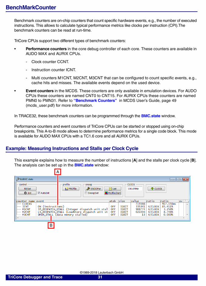
Example: Measuring Instructions and Stalls per Clock Cycle
This example explains how to measure the number of instructions [A] and the stalls per clock cycle [B]. The analysis can be set up in the BMC.state window:
A
B
TriCore Debugger and Trace 31 ©1989-2018 Lauterbach GmbH
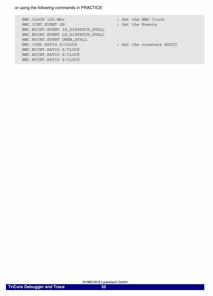
or using the following commands in PRACTICE:
BMC.CLOCK 100.MhzBMC.ICNT.EVENT ONBMC.M1CNT.EVENT IP_DISPATCH_STALL BMC.M2CNT.EVENT LS_DISPATCH_STALLBMC.M3CNT.EVENT DMEM_STALLBMC.ICNT.RATIO X/CLOCKBMC.M1CNT.RATIO X/CLOCK BMC.M2CNT.RATIO X/CLOCKBMC.M3CNT.RATIO X/CLOCK
; Set the BMC Clock; Set the Events
; Set the counters RATIO
TriCore Debugger and Trace 32 ©1989-2018 Lauterbach GmbH
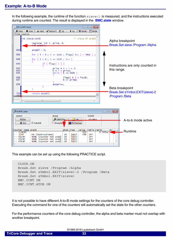
Example: A-to-B Mode
In the following example, the runtime of the function sieve() is measured, and the instructions executed during runtime are counted. The result is displayed in the BMC.state window.
This example can be set up using the following PRACTICE script.
It is not possible to have different A-to-B mode settings for the counters of the core debug controller. Executing the command for one of the counters will automatically set the state for the other counters.
For the performance counters of the core debug controller, the alpha and beta marker must not overlap with another breakpoint.
CLOCK.ONBreak.Set sieve /Program /AlphaBreak.Set sYmbol.EXIT(sieve)-2 /Program /BetaBreak.Set sYmbol.EXIT(sieve)BMC.ICNT ONBMC.ICNT.ATOB ON
Alpha breakpointBreak.Set sieve /Program /Alpha
Beta breakpointBreak.Set sYmbol.EXIT(sieve)-2 /Program /Beta
Instructions are only counted in this range.
A-to-b mode active
Runtime
TriCore Debugger and Trace 33 ©1989-2018 Lauterbach GmbH
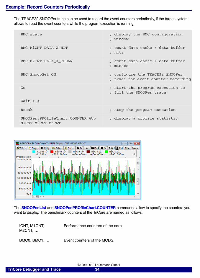
Example: Record Counters Periodically
The TRACE32 SNOOPer trace can be used to record the event counters periodically, if the target system allows to read the event counters while the program execution is running.
The SNOOPer.List and SNOOPer.PROfileChart.COUNTER commands allow to specify the counters you want to display. The benchmark counters of the TriCore are named as follows.
BMC.state ; display the BMC configuration; window
BMC.M1CNT DATA_X_HIT ; count data cache / data buffer; hits
BMC.M2CNT DATA_X_CLEAN ; count data cache / data buffer; misses
BMC.SnoopSet ON ; configure the TRACE32 SNOOPer; trace for event counter recording
Go ; start the program execution to ; fill the SNOOPer trace
Wait 1.s
Break ; stop the program execution
SNOOPer.PROfileChart.COUNTER %Up M1CNT M2CNT M3CNT
; display a profile statistic
ICNT, M1CNT, M2CNT, …
Performance counters of the core.
BMC0, BMC1, … Event counters of the MCDS.
TriCore Debugger and Trace 34 ©1989-2018 Lauterbach GmbH
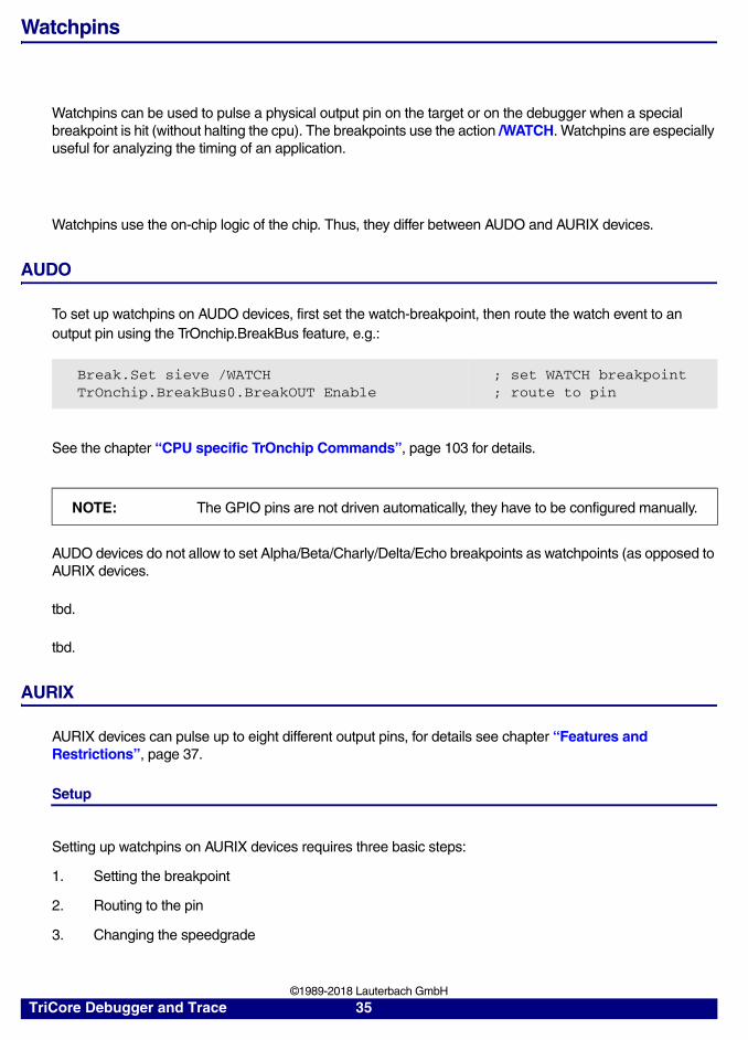
Watchpins
Watchpins can be used to pulse a physical output pin on the target or on the debugger when a special breakpoint is hit (without halting the cpu). The breakpoints use the action /WATCH. Watchpins are especially useful for analyzing the timing of an application.
Watchpins use the on-chip logic of the chip. Thus, they differ between AUDO and AURIX devices.
AUDO
To set up watchpins on AUDO devices, first set the watch-breakpoint, then route the watch event to an output pin using the TrOnchip.BreakBus feature, e.g.:
See the chapter “CPU specific TrOnchip Commands”, page 103 for details.
AUDO devices do not allow to set Alpha/Beta/Charly/Delta/Echo breakpoints as watchpoints (as opposed to AURIX devices.
tbd.
tbd.
AURIX
AURIX devices can pulse up to eight different output pins, for details see chapter “Features and Restrictions”, page 37.
Setup
Setting up watchpins on AURIX devices requires three basic steps:
1. Setting the breakpoint
2. Routing to the pin
3. Changing the speedgrade
Break.Set sieve /WATCHTrOnchip.BreakBus0.BreakOUT Enable
; set WATCH breakpoint; route to pin
NOTE: The GPIO pins are not driven automatically, they have to be configured manually.
TriCore Debugger and Trace 35 ©1989-2018 Lauterbach GmbH
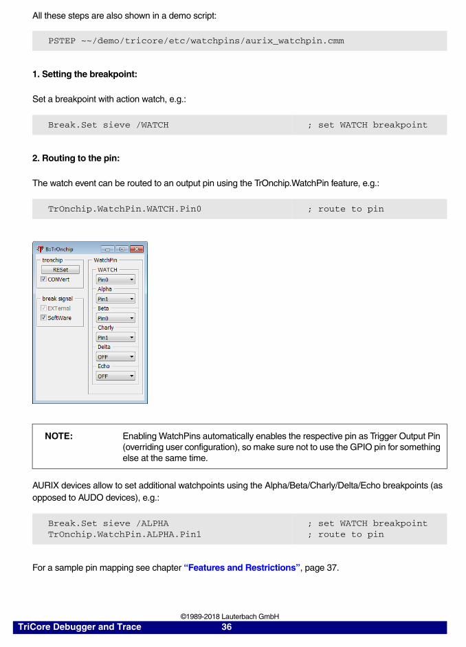
All these steps are also shown in a demo script:
1. Setting the breakpoint:
Set a breakpoint with action watch, e.g.:
2. Routing to the pin:
The watch event can be routed to an output pin using the TrOnchip.WatchPin feature, e.g.:
AURIX devices allow to set additional watchpoints using the Alpha/Beta/Charly/Delta/Echo breakpoints (as opposed to AUDO devices), e.g.:
For a sample pin mapping see chapter “Features and Restrictions”, page 37.
PSTEP ~~/demo/tricore/etc/watchpins/aurix_watchpin.cmm
Break.Set sieve /WATCH ; set WATCH breakpoint
TrOnchip.WatchPin.WATCH.Pin0 ; route to pin
NOTE: Enabling WatchPins automatically enables the respective pin as Trigger Output Pin (overriding user configuration), so make sure not to use the GPIO pin for something else at the same time.
Break.Set sieve /ALPHATrOnchip.WatchPin.ALPHA.Pin1
; set WATCH breakpoint; route to pin
TriCore Debugger and Trace 36 ©1989-2018 Lauterbach GmbH
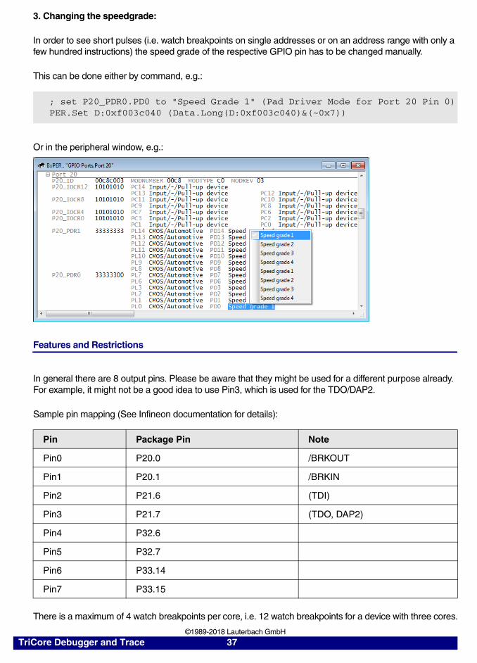
3. Changing the speedgrade:
In order to see short pulses (i.e. watch breakpoints on single addresses or on an address range with only a few hundred instructions) the speed grade of the respective GPIO pin has to be changed manually.
This can be done either by command, e.g.:
Or in the peripheral window, e.g.:
Features and Restrictions
In general there are 8 output pins. Please be aware that they might be used for a different purpose already. For example, it might not be a good idea to use Pin3, which is used for the TDO/DAP2.
Sample pin mapping (See Infineon documentation for details):
There is a maximum of 4 watch breakpoints per core, i.e. 12 watch breakpoints for a device with three cores.
; set P20_PDR0.PD0 to "Speed Grade 1" (Pad Driver Mode for Port 20 Pin 0)PER.Set D:0xf003c040 (Data.Long(D:0xf003c040)&(~0x7))
Pin Package Pin Note
Pin0 P20.0 /BRKOUT
Pin1 P20.1 /BRKIN
Pin2 P21.6 (TDI)
Pin3 P21.7 (TDO, DAP2)
Pin4 P32.6
Pin5 P32.7
Pin6 P33.14
Pin7 P33.15
TriCore Debugger and Trace 37 ©1989-2018 Lauterbach GmbH
The most restrictive part is the availability of the internal lines for routing the watch breakpoints. There are 7 lines, but some of them are already preoccupied:
• Two of them are already occupied internally
• One line is occupied per core
So there are 2-4 lines still available to be routed dynamically (e.g. 4 lines available for a single-core device, 2 lines when multi-core debugging a device with three cores). TRACE32 tries to find an optimal routing.
To sum up, at most 4 different pins can be used at the same time. Still, multiple watch breakpoints can be routed to the same output pin. This might be especially useful when no more resources are available.
TriCore Debugger and Trace 38 ©1989-2018 Lauterbach GmbH
Cache Access
Please see the CACHE command group to directly view the cache contents.
Cache contents can be displayed in various windows by changing the access class, e.g. with:
• Data.dump DC:0x80000000
instead of
• Data.dump D:0x80000000
Use SYStem.Option DCREAD ON to redirect all data memory accesses (D:) to cached data memory accesses (DC:). This is especially useful when displaying variables in the Var.Watch / Var.View window, because they will then be displayed from the CPUs point of view. Please note that cache access is not possible during CPU runtime.
AURIX Devices
Enabling cache access:
• All early AURIX devices (TC27x-Astep, TC2Dx) do not need special handling for cache access.
• All later devices (TC27x-Bstep, TC29x, TC26x, …) implement the caches differently: As soon as cache access is enabled, the devices follow a security requirement cleaning the cache contents. Thus, access has to be enabled either at startup or manually.
- TRACE32 will automatically enable cache access when starting the device with SYStem.Up.
- When starting the device with SYStem.Mode.Go or attaching to it with SYStem.Mode.Attach, cache access cannot be enabled automatically. In this case, cache access can be enabled manually by invalidating the cache with CACHE.INVALIDATE.IC or CACHE.INVALIDATE.DC. Manual invalidation can also be triggered when the CACHE.DUMP window shows bus error.
Due to the chip internal structure of the cache it may happen, that a cache line is already marked as valid while its contents are not yet updated. Executing an isync or dsync instruction will guarantee synchronicity.
Please note that TC1.6E (efficiency) cores implement a small data read buffer instead of a data cache. The data read buffer is not accessible by TRACE32.
TriCore Debugger and Trace 39 ©1989-2018 Lauterbach GmbH
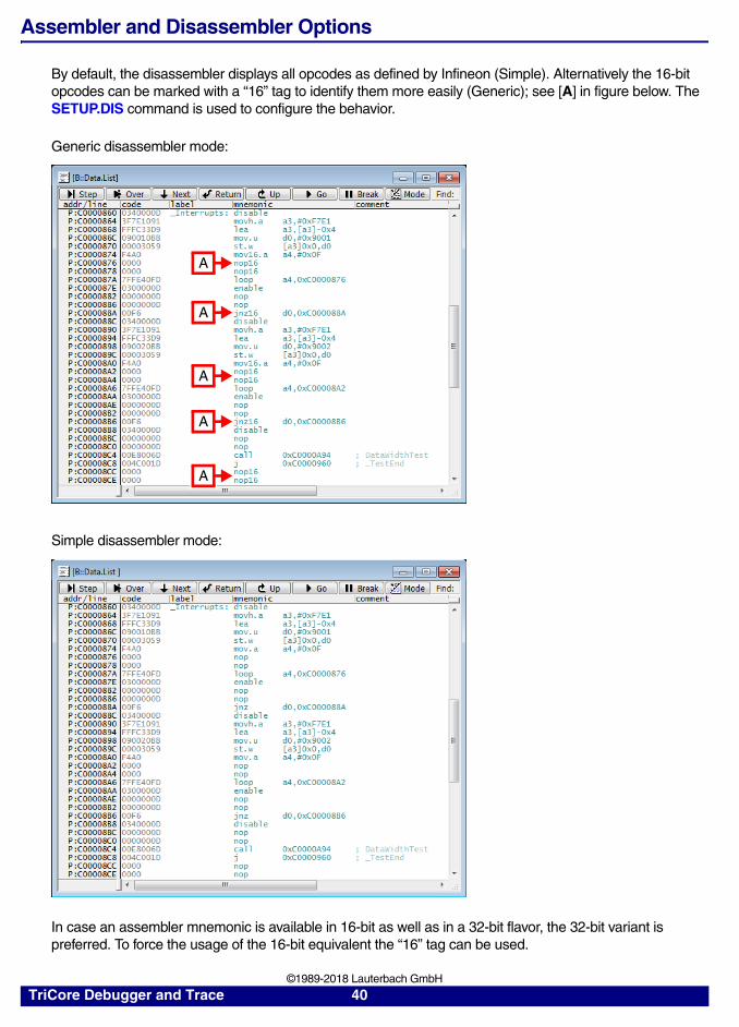
Assembler and Disassembler Options
By default, the disassembler displays all opcodes as defined by Infineon (Simple). Alternatively the 16-bit opcodes can be marked with a “16” tag to identify them more easily (Generic); see [A] in figure below. The SETUP.DIS command is used to configure the behavior.
Generic disassembler mode:
Simple disassembler mode:
In case an assembler mnemonic is available in 16-bit as well as in a 32-bit flavor, the 32-bit variant is preferred. To force the usage of the 16-bit equivalent the “16” tag can be used.
A
A
A
A
A
TriCore Debugger and Trace 40 ©1989-2018 Lauterbach GmbH
Parallel Usage of a 3rd-Party Tool
Some 3rd-party tools require access to the debug port and/or debug resources as well. Examples of 3rd-party tools are tools for measurement, calibration and data-stimulation (MC tools). This section describes how to use such a 3rd-party tool in parallel with TRACE32.
There are different options of how to share the debug port. The appropriate method depends on the 3rd-party tool. In general, TRACE32 supports the following options:
• Software debugging over XCP: In this mode, all debug commands are send to the 3rd-party tool using the standardized XCP protocol. For details, see “XCP Debug Back-End” (backend_xcp.pdf).
• Physical sharing: In this mode, the debug signals are shared using a special debug adapter for the 3rd-party tool. This mode is described in the next section.
The 3rd-party tool might also require certain debug resources of the target CPU. Typical examples are:
• The Core Debug Controller covers all debug resources that are part of the CPU like hardware breakpoints.
• The Cerberus block (CBS) covers all chip-wide debug resources. See also “Cerberus Access Protection”, page 49.
• Emulation Memory can be divided up between a calibration tool and TRACE32 to allow calibration and tracing in parallel. For details and configuration, please refer to chapter “Emulation Memory” (mcds_user.pdf).
You must make sure TRACE32 is not trying to use these resources in parallel, e.g. by special configuration. Examples for known 3rd-party tools can be found under ~~/demo/tricore/etc/. In doubt, please contact Lauterbach and/or the 3rd-party tool vendor.
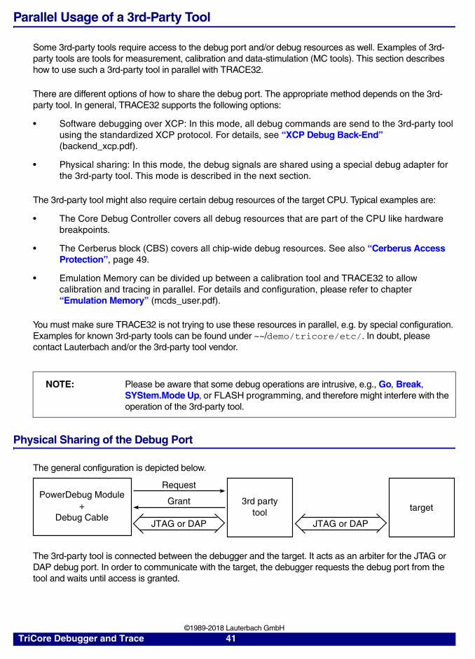
Physical Sharing of the Debug Port
The general configuration is depicted below.
The 3rd-party tool is connected between the debugger and the target. It acts as an arbiter for the JTAG or DAP debug port. In order to communicate with the target, the debugger requests the debug port from the tool and waits until access is granted.
NOTE: Please be aware that some debug operations are intrusive, e.g., Go, Break, SYStem.Mode Up, or FLASH programming, and therefore might interfere with the operation of the 3rd-party tool.
PowerDebug Module+
Debug CableJTAG or DAP
Request
Grant 3rd partytool
JTAG or DAP
target
TriCore Debugger and Trace 41 ©1989-2018 Lauterbach GmbH
Sharing of the debug port must be configured using SYStem.CONFIG PortSHaRing before bringing the system up. Typical start-up sequences:
• JTAG (e.g., ETAS ETK for AUDO CPUs):
The JTAG clock must be between 10 MHz (default) and 40 MHz.
• DAP (e,g., ETAS ETK-S20 for AURIX CPUs):
For the most common CPUs and 3rd-party tools, PRACTICE start-up scripts (*.cmm) can be found under ~~/demo/tricore/etc/.
Avoid displaying invalid memory locations (Bus Error).
Details about electrical requirements and connector pin-outs can be found in “Application Note Debug Cable TriCore” (tricore_app_ocds.pdf).
SYStem.CPU TC1796ED ; select your CPU
SYStem.CONFIG DEBUGPORTTYPE JTAG ; switch debug port to JTAG
SYStem.CONFIG PortSHaRing ON ; enable port sharing
SYStem.CONFIG TCKLEVEL 0 ; pull-down on TCK (default)
SYStem.CONFIG TAPState 12. ; Run-Test/Idle (default)
SYStem.Mode Attach ; connect to CPU
SYStem.CPU TC277TE ; select your CPU
SYStem.CONFIG DEBUGPORTTYPE DAP2 ; switch debug port to DAP
SYStem.CONFIG PortSHaRing ON ; enable port sharing
SYStem.Mode Attach ; connect to CPU
PSTEP ~~/demo/tricore/etc/etk/*.cmm ; step through a demo; script
TriCore Debugger and Trace 42 ©1989-2018 Lauterbach GmbH
Debugging an Application with the Memory Protection Unit Enabled
Debugging a TriCore device with the Memory Protection Unit enabled requires different device-dependent strategies.
TriCore v1.6 and Later
For TriCore devices with core architecture v1.6 and later, the Memory Protection Unit and the on-chip breakpoint implementation have been separated. Debugging such a device with the MPU enabled does not require any specific setup or configuration.
TriCore v1.3.1 and Earlier
TriCore devices with a core architecture up to v1.3.1 have the on-chip breakpoint feature implemented in the Memory Protection Unit. This means that either on-chip breakpoints or the MPU can be used, but not both at the same time. Do not activate the MPU for single stepping on assembler level.
For simplification debugging an application in RAM is explained first, then the additional configuration for an application located in FLASH.
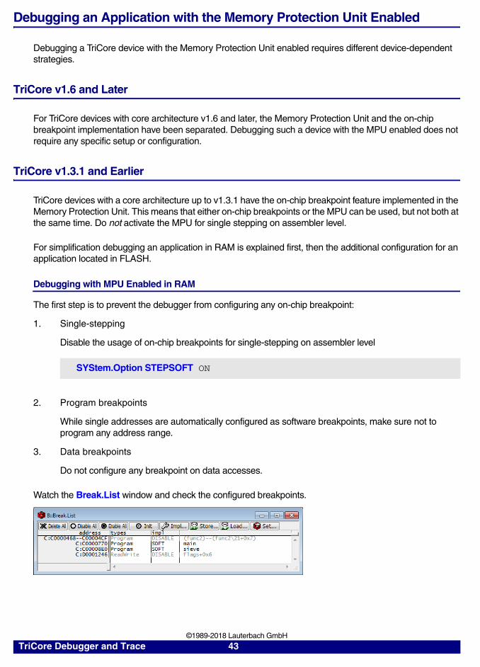
Debugging with MPU Enabled in RAM
The first step is to prevent the debugger from configuring any on-chip breakpoint:
1. Single-stepping
Disable the usage of on-chip breakpoints for single-stepping on assembler level
2. Program breakpoints
While single addresses are automatically configured as software breakpoints, make sure not to program any address range.
3. Data breakpoints
Do not configure any breakpoint on data accesses.
Watch the Break.List window and check the configured breakpoints.
SYStem.Option STEPSOFT ON
TriCore Debugger and Trace 43 ©1989-2018 Lauterbach GmbH
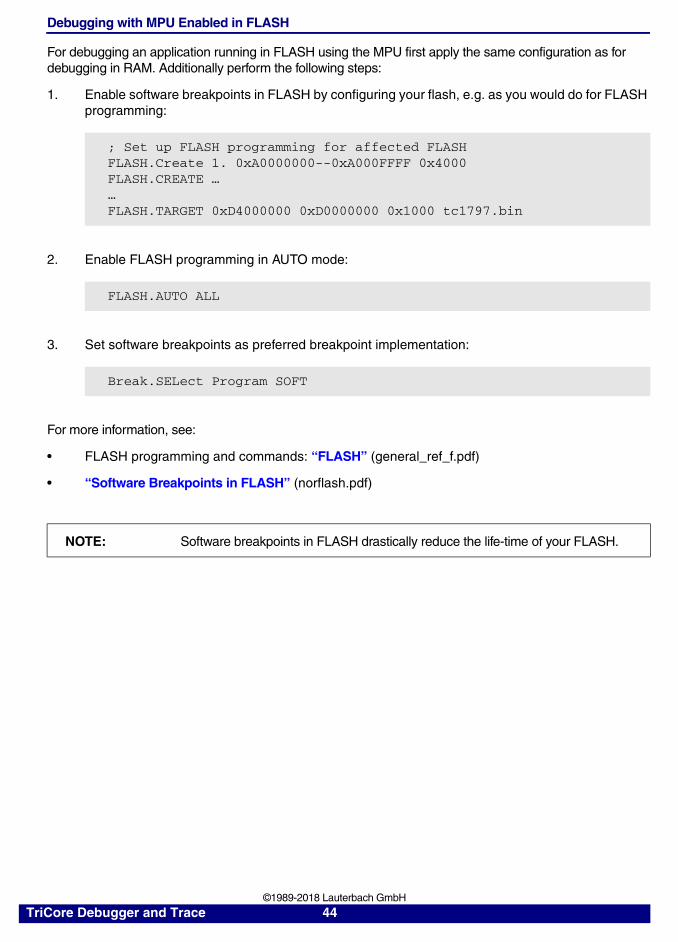
Debugging with MPU Enabled in FLASH
For debugging an application running in FLASH using the MPU first apply the same configuration as for debugging in RAM. Additionally perform the following steps:
1. Enable software breakpoints in FLASH by configuring your flash, e.g. as you would do for FLASH programming:
2. Enable FLASH programming in AUTO mode:
3. Set software breakpoints as preferred breakpoint implementation:
For more information, see:
• FLASH programming and commands: “FLASH” (general_ref_f.pdf)
• “Software Breakpoints in FLASH” (norflash.pdf)
; Set up FLASH programming for affected FLASHFLASH.Create 1. 0xA0000000--0xA000FFFF 0x4000FLASH.CREATE ……FLASH.TARGET 0xD4000000 0xD0000000 0x1000 tc1797.bin
FLASH.AUTO ALL
Break.SELect Program SOFT
NOTE: Software breakpoints in FLASH drastically reduce the life-time of your FLASH.
TriCore Debugger and Trace 44 ©1989-2018 Lauterbach GmbH
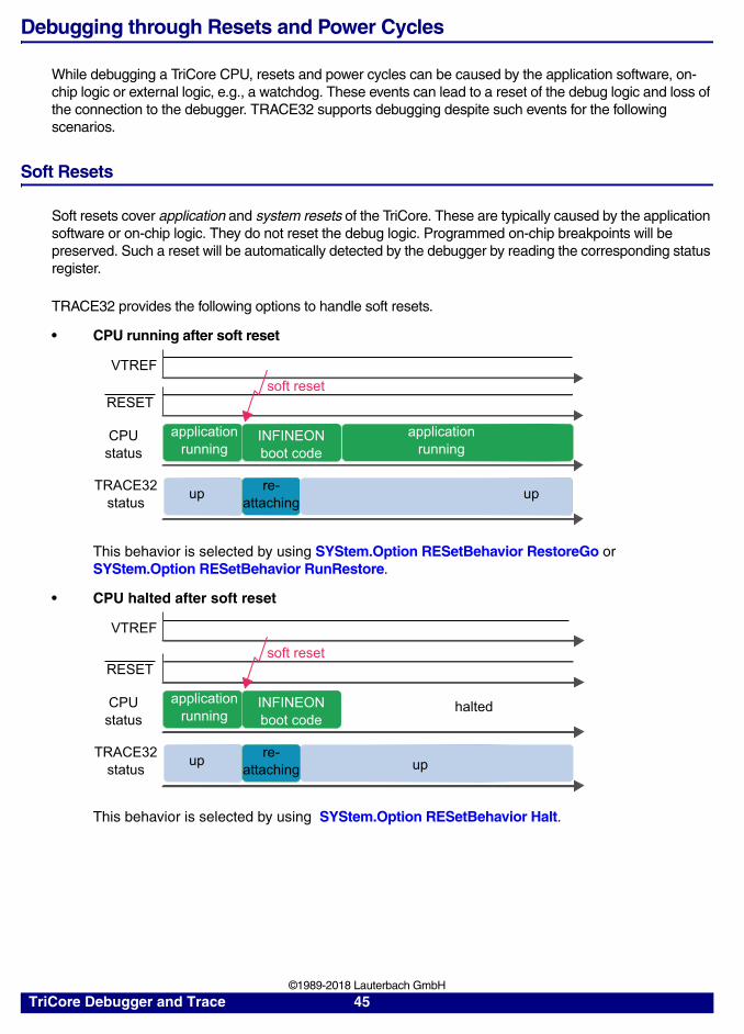
Debugging through Resets and Power Cycles
While debugging a TriCore CPU, resets and power cycles can be caused by the application software, on-chip logic or external logic, e.g., a watchdog. These events can lead to a reset of the debug logic and loss of the connection to the debugger. TRACE32 supports debugging despite such events for the following scenarios.
Soft Resets
Soft resets cover application and system resets of the TriCore. These are typically caused by the application software or on-chip logic. They do not reset the debug logic. Programmed on-chip breakpoints will be preserved. Such a reset will be automatically detected by the debugger by reading the corresponding status register.
TRACE32 provides the following options to handle soft resets.
• CPU running after soft reset
This behavior is selected by using SYStem.Option RESetBehavior RestoreGo or SYStem.Option RESetBehavior RunRestore.
• CPU halted after soft reset
This behavior is selected by using SYStem.Option RESetBehavior Halt.
VTREF
RESET
INFINEONboot code
CPUstatus
applicationrunning
TRACE32status up re-
attaching up
applicationrunning
soft reset
INFINEONboot code
haltedCPUstatus
TRACE32status
applicationrunning
RESET
VTREF
up upre-
attaching
soft reset
TriCore Debugger and Trace 45 ©1989-2018 Lauterbach GmbH
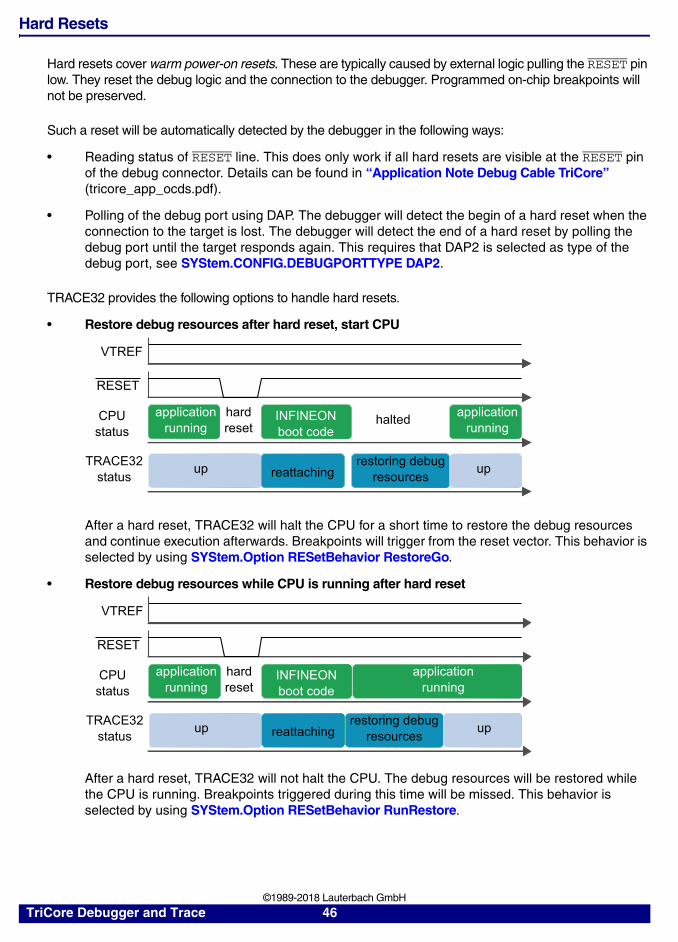
Hard Resets
Hard resets cover warm power-on resets. These are typically caused by external logic pulling the RESET pin low. They reset the debug logic and the connection to the debugger. Programmed on-chip breakpoints will not be preserved.
Such a reset will be automatically detected by the debugger in the following ways:
• Reading status of RESET line. This does only work if all hard resets are visible at the RESET pin of the debug connector. Details can be found in “Application Note Debug Cable TriCore” (tricore_app_ocds.pdf).
• Polling of the debug port using DAP. The debugger will detect the begin of a hard reset when the connection to the target is lost. The debugger will detect the end of a hard reset by polling the debug port until the target responds again. This requires that DAP2 is selected as type of the debug port, see SYStem.CONFIG.DEBUGPORTTYPE DAP2.
TRACE32 provides the following options to handle hard resets.
• Restore debug resources after hard reset, start CPU
After a hard reset, TRACE32 will halt the CPU for a short time to restore the debug resources and continue execution afterwards. Breakpoints will trigger from the reset vector. This behavior is selected by using SYStem.Option RESetBehavior RestoreGo.
• Restore debug resources while CPU is running after hard reset
After a hard reset, TRACE32 will not halt the CPU. The debug resources will be restored while the CPU is running. Breakpoints triggered during this time will be missed. This behavior is selected by using SYStem.Option RESetBehavior RunRestore.
VTREF
RESET
INFINEONboot code
haltedCPUstatus
hardreset
applicationrunning
TRACE32status up reattaching uprestoring debug
resources
applicationrunning
VTREF
RESET
INFINEONboot code
CPUstatus
hardreset
applicationrunning
TRACE32status up reattaching uprestoring debug
resources
applicationrunning
TriCore Debugger and Trace 46 ©1989-2018 Lauterbach GmbH
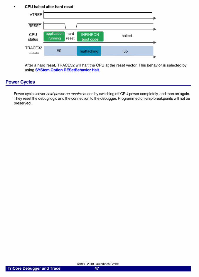
• CPU halted after hard reset
After a hard reset, TRACE32 will halt the CPU at the reset vector. This behavior is selected by using SYStem.Option RESetBehavior Halt.
Power Cycles
Power cycles cover cold power-on resets caused by switching off CPU power completely, and then on again. They reset the debug logic and the connection to the debugger. Programmed on-chip breakpoints will not be preserved.
INFINEONboot code
haltedCPUstatus
TRACE32status
hardreset
applicationrunning
RESET
VTREF
up reattaching up
TriCore Debugger and Trace 47 ©1989-2018 Lauterbach GmbH

The debugger will automatically detect a power cycle by observing the VTREF pin of the debug connector. Details can be found in “Application Note Debug Cable TriCore” (tricore_app_ocds.pdf). Debugging through power cycles is supported by TRACE32 if SYStem.Mode StandBy is selected beforehand. The following options are available:
• Restore debug resources after power cycle, start CPU
After detecting the end of a power cycle, TRACE32 will halt the CPU for a short time to restore the debug resources. Breakpoints will trigger from the reset vector. This behavior is selected by using SYStem.Option RESetBehavior RestoreGo.
• Restore debug resources while CPU is running after power cycle
After detecting the end of a power cycle, TRACE32 will not halt the CPU. The debug resources will be restored while the CPU is running. Breakpoints triggered during this time will be missed. This behavior is selected by using SYStem.Option RESetBehavior RunRestore.
• CPU halted after power cycle
After detecting the end of a power cycle, TRACE32 will halt the CPU at the reset vector. This behavior is selected by using SYStem.Option RESetBehavior Halt.
VTREF
RESET
INFINEONboot code
CPUstatus off
applicationrunning
TRACE32status
up(standby) reattaching
restoring debugresources
applicationrunning
standbyup
(standby)
halted
VTREF
RESET
INFINEONboot code
CPUstatus off
applicationrunning
TRACE32status
up(standby) reattaching
restoring debugresources
applicationrunning
standbyup
(standby)
VTREF
RESET
INFINEONboot code
CPUstatus off
applicationrunning
TRACE32status
up(standby) reattaching
restoring debugresources
applicationrunning
standbyup
(standby)
halted
TriCore Debugger and Trace 48 ©1989-2018 Lauterbach GmbH
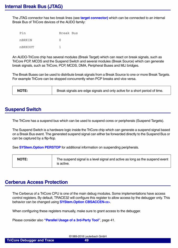
Internal Break Bus (JTAG)
The JTAG connector has two break lines (see target connector) which can be connected to an internal Break Bus of TriCore devices of the AUDO family:
An AUDO-TriCore chip has several modules (Break Target) which can react on break signals, such as TriCore PCP, MCDS and the Suspend Switch and several modules (Break Source) which can generate break signals, such as TriCore, PCP, MCDS, DMA, Peripheral Buses and MLI bridges.
The Break Buses can be used to distribute break signals from a Break Source to one or more Break Targets. For example TriCore can be stopped concurrently when PCP breaks and vice versa.
Suspend Switch
The TriCore has a suspend bus which can be used to suspend cores or peripherals (Suspend Targets).
The Suspend Switch is a hardware logic inside the TriCore chip which can generate a suspend signal based on a Break Bus event. The generated suspend signal can either be forwarded directly to the Suspend Bus or can be captured by a flip-flop.
See SYStem.Option PERSTOP for additional information on suspending peripherals.
Cerberus Access Protection
The Cerberus of a TriCore CPU is one of the main debug modules. Some implementations have access control registers. By default, TRACE32 will configure this register to allow access by the debugger only. This behavior can be changed using SYStem.Option CBSACCEN<x>.
When configuring these registers manually, make sure to grant access to the debugger.
Please consider also “Parallel Usage of a 3rd-Party Tool”, page 41.
Pin Break Bus
nBRKIN 0
nBRKOUT 1
NOTE: Break signals are edge signals and only active for a short period of time.
NOTE: The suspend signal is a level signal and active as long as the suspend event is active.
TriCore Debugger and Trace 49 ©1989-2018 Lauterbach GmbH

Troubleshooting
In this section:
• SYStem.Up Errors
• Debugging Optimized Code
• Please also see the chapter “FAQ”, page 52.
SYStem.Up Errors
The SYStem.Up command is the first command of a debug session where communication with the target is required. If you receive error messages while executing this command this may have the following reasons.
• The target has no power or the debug connector is mounted in wrong orientation.
• External controlled /RESET line:
The debugger controls the processor reset and uses the /RESET line to reset the CPU on most of the SYStem.Mode commands. Therefore only non-active, open-drain driver may be connected to this signal.
• There is logic added to the JTAG signals:
The debugger supports multi-processor debugging only in certain cases. When inserting other processors in the JTAG chain, TriCore must be the first processor. No other TriCore and no processor with a Cerberus based JTAG interface (e.g. XC16x, XC2000) are allowed in the chain.
• There are additional loads or capacities on the JTAG line.
For more information on pins, signals and daisy-chaining please refer to “Debug Interface Configuration” (tricore_app_ocds.pdf).
Debugging Optimized Code
It is recommended to debug applications with compiler-optimizations turned off. However, this is not always possible.
Optimized code often splits a single HLL line into multiple blocks of non-consecutive assembler instructions. Depending on the compiler a single HLL line can generate multiple blocks of code, making single stepping fiddly and setting breakpoints complex.
Such lines can be summarized when loading an application with the Data.LOAD command:
• The /SingleLineAdjacent option summarizes adjacent blocks of assembler code generated for an HLL line.
• The /SingleLine option summarizes blocks of assembler code generated for an HLL line.
For example:
Data.LOAD.Elf my_application.elf /SingleLineAdjacent
TriCore Debugger and Trace 50 ©1989-2018 Lauterbach GmbH
These options are explained in detail in chapter “Details on Generic Load Options” in General Commands Reference Guide D, page 80 (general_ref_d.pdf).
TriCore Debugger and Trace 51 ©1989-2018 Lauterbach GmbH
FAQ
Debugging via VPN
Ref: 0307
The debugger is accessed via Internet/VPN and the performance is very slow. What can be done to improve debug performance?
The main cause for bad debug performance via Internet or VPN are low data throughput and high latency. The ways to improve performance by the debugger are limited:
In PRACTICE scripts, use "SCREEN.OFF" at the beginning of the scriptand "SCREEN.ON" at the end. "SCREEN.OFF" will turn off screenupdates. Please note that if your program stops (e.g. on error) without exe-cuting "SCREEN.OFF", some windows will not be updated.
"SYStem.POLLING SLOW" will set a lower frequency for target statechecks (e.g. power, reset, jtag state). It will take longer for the debugger torecognize that the core stopped on a breakpoint.
"SETUP.URATE 1.s" will set the default update frequency ofData.List/Data.dump/Variable windows to 1 second (the slowest possiblesetting).
prevent unneeded memory accesses using "MAP.UPDATEONCE[address-range]" for RAM and "MAP.CONST [address--range]" forROM/FLASH. Address ranged with "MAP.UPDATEONCE" will read thespecified address range only once after the core stopped at a breakpoint ormanual break. "MAP.CONST" will read the specified address range onlyonce per SYStem.Mode command (e.g. SYStem.Up).
TriCore Debugger and Trace 52 ©1989-2018 Lauterbach GmbH
Setting a Software Breakpoint fails
Ref: 0276
What can be the reasons why setting a software breakpoint fails?
Setting a software breakpoint can fail when the target HW is not able to implement the wanted breakpoint. Possible reasons:
The wanted breakpoint needs special features that are only possible torealize by the trigger unit inside the controller.
Example: Read, write and access (Read/Write) breakpoints ("type" in Break.Set window). Breakpoints with checking in real-time for data-values ("Data"). Breakpoints with special features ("action") like TriggerTrace, TraceEnable, TraceOn/TraceOFF.
TRACE32 can not change the memory.Example: ROM and Flash when no preparation with FLASH.Create, FLASH.TARGET and FLASH.AUTO was made. All type of memory if the memory device is missing the necessary control signals like WriteEnable or settings of registers and SpecialFunctionRegisters (SFR).
Contrary settings in TRACE32.Like: MAP.BOnchip for this memory range. Break.SELect.<breakpoint-type> Onchip (HARD is only available for ICE and FIRE).
RTOS and MMU:If the memory can be changed by Data.Set but the breakpoint doesn't work it might be a problem of using an MMU on target when setting the breakpoint to a symbolic address that is different than the writable and intended memory location.
Breakpoints in Peripherals Modules
Ref: 0170
When setting a read/write breakpoint to a peripheral module the program execution is not stopped.
The comparators used by the on-chip breakpoints only have an effect on non-peripheral address segments. As a workaround, the breakpoint registers in the LMI Bridge can be programmed manually.
TriCore Debugger and Trace 53 ©1989-2018 Lauterbach GmbH
CPU "stopped by XXXevt"
Ref: 0283
When the CPU has halted the debugger shows "stopped by swevt" or "stopped by tr0evt".
The message in the status bar reflects the current state of the CPU, and probably why it has reached this state.
stopped
The CPU has stopped because the user issued the Break command.
stopped by breakpoint
The CPU has stopped because of a breakpoint condition (software or on-chip), and the breakpoint condition was set up via the debugger (e.g. Break.Set command).
stopped by XXXevt
The TriCore CPU has stopped due to an event not triggered by the debugger. It shows the reason reported in the Debug Status Register, where XXXevt can be
swevt
software event, the CPU has executed a debug or debug16 instruction
extevt
external event, e.g. event on nBRKIN line via the JTAG cable
crevt
access to a Core Special Function Register (SFR) (feature not used by debugger)
tr0evt or tr1evt
Memory Protection event, normally used by on-chip breakpoints
stopped by unknown
An unknown event has occured, the CPU is probably in some undefined state. When using Target Based Flash Programming, the debugger shows "stopped by swevt" after each flash programming or erase action.
FLOWERROR when using OCDS-L2 Trace
Ref: 0188
For my TriBoard-TC1766 I have set up my trace configuration correctly, but all I get is FLOWERROR.
On some older TriBoards-TC1766 (below version .300) two trace lines are swapped. Use "SYStem.Option TB1766FIX ON" for correcting this by software.
TriCore Debugger and Trace 54 ©1989-2018 Lauterbach GmbH
Interrupt taken on single-step
Ref: 0398
When single-stepping I always enter the interrupt handler although IMASKASM and IMASKHLL is enabled.
Some devices with a TriCore v1.3.1 core have a silicon issue that an acknowlegded interrupt is always taken, even if interrupts are disabled after acknowlege. This is documented as Errata CPU_TC.115. Affected devices: TC1167, TC1197, TC1736, TC1767, TC1797 and corresponding Emulation Devices. Worarkound:
Disable interrupts permanently while single-stepping.
Enable SYStem.Option STEPSOFT (RAM) or SYStem.Option STEPON-CHIP (RAM, FLASH). This will not prevent the interrupt from being takenbut will execute the interrupt handler silently in background.
Further documentation:
Infineon User Documentation for your device
Infineon Errata Sheet for your device (CPU_TC.115)
TRACE32 Processor Architecture Manual for TriCore, chapters
Debugging, Single Stepping
Command Reference, SYStem.Option STEPONCHIP
Command Reference, SYStem.Option STEPSOFT
On-chip Breakpoints and Memory Protection
Ref: 0198
When using on-chip breakpoints, the Memory Protection Registers are overwritten.
Up to core version 1.3.1 the TriCore architecture intends using the Memory Protection Registers for implementing on-chip breakpoints. This means that you can not have on-chip breakpoints and memory protection at the same time. When debugging, the Memory Protection is normally not needed and should be disabled. You may want to configure your RTOS to do this automatically when a debugger is detected. Use "SYStem.Option STEPSOFT ON" for debugging your Memory Protection Unit. With some additional configuration, this is also possible from FLASH memory. Make sure to set only software-breakpoints, e.g. by setting "Break.IMPLementation Program SOFT". Additionally, on TC v1.3.1 devices, you might want to set "SYStem.Option BREAKFIX OFF".
TriCore Debugger and Trace 55 ©1989-2018 Lauterbach GmbH
Single Step after SYStem.Mode Attach
Ref: 0173
When switching to SYStem.Mode Attach, the CPU can be stopped and started but breakpoints are not working.
For older TriCore deriviatives (e.g. Rider-D, TC10GP, TC17x5, TC19x0, ...) OCDS can only be enabled at reset. When attaching, the target is running and reset has already been performed. If you want to use breakpoints and single stepping, you have to pull nBRKIN and nOCDSE to ground at reset. This does not apply to newer TriCore CPUs such as AUDO-NG, AUDO-FUTURE or newer.
Single stepping seems to hang
Ref: 0415
Single stepping seems to hang when debugging optimized code.
When stepping through optimized code, TRACE32 sometimes seems not to execute the step correctly, the program counter (PC) remains at the same HLL line for multiple steps. The List window usually shows a drill-down box (a + sign) next to the line number. This is a result of the compiler settings and compiler output. As a workaround, summarize adjacent blocks of assembler code when loading an application, e.g. with Data.LOAD.Elf my_application.elf /SingleLineAdjacent . Please see chapter "Debugging Optimized Code" in the TriCore Processor Architecture Manual (debugger_tricore.pdf) for details.
SMU Alarm is raised
Ref: 0433
Why does the TriCore chip show that an SMU alarm was raised?
If the SMU is set up strict, some debugger accesses might cause an SMU Alarm (SRI bus error), because the chip can not differentiate between illegal and debugger accesses.
Usually this is caused when the debugger tries to set software breakpoints on a flash memory region. Use the command MAP.BOnchip <addressrange> to force the debugger to set onchip breakpoints in the respective memory region.
To prevent all debugger accesses to a certain memory region, the command MAP.DenyAccess <addressrange> can be used.
TriCore Debugger and Trace 56 ©1989-2018 Lauterbach GmbH
Unable to break TriCore, debugger shows "running (PLL lock wait)".
Ref: 0394
After SYStem.Mode Up the target is running and the debugger shows "running (PLL lock wait)". How can I stop program execution?
The information that the PLL is not locked is read by the debugger from the register PMSCR located in the SCU. Whether the PLL is locked or not does not affect the debug connection, so this is not an error but an information. However this CPU state is often observed in cases where the debugger seems to have a debug connection established but the target does not respond to debugger commands such as break. Although the debug connection is broken completely, the debugger thinks to get valid responses from the target withput being able to recognize that they are invalid. So for the debugger the target state is that the TriCore is running and the PLL is not locked. An additional check that the debug connection is not working correctly is performing a JTAG chain scan. For this, execute "Menu -> Help -> Support -> Systeminfo..." and check the results at the end of the file in section "JTAG Chain": If the chain scan failed and you see a message such as "TDO stays constantly low" there is no target connection possible with this device. There may be two main reasons: Either there is a physical or logical connection problem, or your TriCore device is broken. You may want to cross-check with another target system or debugger. Remove all extension cords and connect the debug cable directly to your target device.
Unable to Erase or Program Flash Memory
Ref: 0190
When using target based flash programming algorithms, flash is not completely erased or programmed.
Target based flash programming algorithms are running on the CPU itself. When the watchdog is not disabled, they are interrupted by the watchdog's reset. See the flash programming demos how to disable the watchdog manually.
Audo-NG
Unable to do a Step or Go Command
Ref: 0189
I have loaded my application into the target, but I can not step or go away from the reset address.
TC11xx and AUDO-NG devices, e.g. TC1766, TC1796, have a silicon bug that prevents the instruction cache from being invalidated when the CPU is halted. Software breakpoints (which are used by default) use the DEBUG16 instruction to halt the processor and are being replaced in memory by the original instruction when the core is released to running state. Due to the silicon bug, the DEBUG16 instruction is still in the instruction cache at this time and will be executed. Workarounds:
Force the debugger to use on-chip breakpoints by default by defining thewhole memory region as ROM/ FLASH: MAP.BOnchip
There is a workaround for forcing the instruction cache to be invalidated.Please see the demoscripts for more information. Be sure to put theinstruction sequence to an address range not used by your application,otherwise it would run into the DEBUG16 instruction.
TriCore Debugger and Trace 57 ©1989-2018 Lauterbach GmbH
AURIX
Board does not boot
Ref: 0414
My Infineon TriBoard does not boot and SYStem.Up fails.
Please make sure the Hardware Book Configuration settings are correct. On Infineon TriBoards there is a DIP switch which allows to modify the HWCFG settings. TC275T-Bstep an later devices usually require DIPSWITCH1 to be off, otherwise the board is not powered correctly (check the voltage LEDs). Please consult the TriBoard Manual or other Infineon documentation for details.
AURIX
JTAG communication does not work
Ref: 0413
JTAG communication is not possible with some AURIX devices.
On some TriCore AURIX devices the TDI pin, which is necessary for JTAG communication, is replaced by the VDDPSB (3.3V) pin. Therefore it is not possible to debug via JTAG. Instead DAP mode can be used (see command SYStem.CONFIG.DEBUGPORTTYPE DAP). Note that currently only Emulation Devices in an LQFP package (except Fusion Quad and TC27x-Astep) are affected, e.g. TC275TE, TC264DE, TC265DE. Please consult the Infineon documentation for details.
AURIX
TRACE32 shows error ambiguous symbol
Ref: 0406
TRACE32 shows error "ambiguous symbol", what can I do about it?
Each TriCore core of an AURIX chip is equipped with directly attached memories: Program Scratch Pad Ram (PSPR) and Data Scratch Pad Ram (DSPR), accessible by itself via core-local and global addressing, accessible by other cores via global addressing. When accessing its own memory, accessing via global addresses has no (!) impact on access speed. When having different code and therefore different symbols on each core, core-local addressing can easily lead to ambiguous symbols. Imagine a function "foo" at address P:0xC0000100 on core 0 and a completely different function "bar" at address P:0xC0000100 on core 1. Using global addressing avoids such ambiguities, in the above example "foo" would be at address P:0x70100100 and "bar" at P:0x60100100 . In general, it is recommended to use global addressing only, avoid core-local-addressing whenever possible. Modify the linker script file in your compiler toolchain.
TC10GP
TriCore Data Cache
Ref: 0207
The debugger displays wrong data for internal memory, but the processor behaves correct.
TC10GP and TC11Ix have a data cache (DCACHE within DMI) which is not accessible by the debugger. The debugger shows invalid internal memory instead. This bug only affects the internal memory. The cache from EMU can be bypassed by switching to the uncached memory segment. As a workarounds, disable the cache. For TC1110, TC1115 and TC1130 this problem is fixed by flushing the cache.
TriCore Debugger and Trace 58 ©1989-2018 Lauterbach GmbH
TC11Ix
TriCore Data Cache
Ref: 0207
The debugger displays wrong data for internal memory, but the processor behaves correct.
TC10GP and TC11Ix have a data cache (DCACHE within DMI) which is not accessible by the debugger. The debugger shows invalid internal memory instead. This bug only affects the internal memory. The cache from EMU can be bypassed by switching to the uncached memory segment. As a workarounds, disable the cache. For TC1110, TC1115 and TC1130 this problem is fixed by flushing the cache.
TC11XX
Unable to do a Step or Go Command
Ref: 0189
I have loaded my application into the target, but I can not step or go away from the reset address.
TC11xx and AUDO-NG devices, e.g. TC1766, TC1796, have a silicon bug that prevents the instruction cache from being invalidated when the CPU is halted. Software breakpoints (which are used by default) use the DEBUG16 instruction to halt the processor and are being replaced in memory by the original instruction when the core is released to running state. Due to the silicon bug, the DEBUG16 instruction is still in the instruction cache at this time and will be executed. Workarounds:
Force the debugger to use on-chip breakpoints by default by defining thewhole memory region as ROM/ FLASH: MAP.BOnchip
There is a workaround for forcing the instruction cache to be invalidated.Please see the demoscripts for more information. Be sure to put theinstruction sequence to an address range not used by your application,otherwise it would run into the DEBUG16 instruction.
TriCore Debugger and Trace 59 ©1989-2018 Lauterbach GmbH
Tracing
Tracing allows an in-depth analysis of the behavior and the timing characteristics of the embedded system.
A trace records information about a program’s execution during runtime, usually including program flow and read/written data. The cores as well as chip internal buses can act as trace sources.
This chapter covers the following topics:
• “On-chip Trace (OCDS-L3)”, page 60
• “Serial Off-Chip Trace”, page 66
• “Parallel Off-Chip Trace”, page 66
Only basic information will be given here, details and advanced tasks are described in separate documents, see “Further Reading”, page 65.
The trace messages for the On-chip Trace and the Serial Off-chip Trace are generated by the MCDS or Mini-MCDS. The MCDS is only implemented in Emulation Devices, the Mini-MCDS in some Product Devices. Please refer to “MCDS User’s Guide” (mcds_user.pdf) for more information.
On-chip Trace (OCDS-L3)
On-chip tracing is only possible with an Infineon Emulation Device (ED), offering the MCDS (MultiCore Debug Solution) for implementing trace triggers, filters and generation of trace messages (MCDS messages).
Use Trace.METHOD Onchip for selecting the on-chip trace.
Quick Start for Tracing with On-chip Trace (OCDS-L3)
It is assumed that you are tracing a TC1766ED B-Step on an Infineon TriBoard-TC1766.300 or above.
1. Prepare the Debugger
Load your application and prepare for debug. For details, see “Single-Core Debugging - Quick Start”, page 15.
TriCore Debugger and Trace 60 ©1989-2018 Lauterbach GmbH
2. Specify Trace Source and Recording Options
Select the core to trace (e.g. TriCore), and what should be recorded (e.g. program flow and timestamps). When enabling timestamps, the CPU clock has to be added also.
3. Start and Stop Tracing
Note that tracing can also be stopped by a breakpoint.
4. View the Results
Supported Features
• Program Flow Trace for TriCore and PCP
• Data Trace for TriCore and PCP
• Ownership Trace for PCP
• FPI Bus Trace (independent of TriCore or PCP), both System Peripheral Bus (SPB) and Remote Peripheral Bus (RPB, if available)
• Timestamps
• Simple Trace Control
See the Onchip.Mode commands for a general setup of the on-chip trace, the MCDS commands and “Basic Trace Usage” (mcds_user.pdf) for a detailed setup of the on-chip MCDS resources.
MCDS.SOURCE TriCore FlowTrace ON ; enable TriCore program flow; trace
MCDS.TimeStamp TICKS ; enable Ticks as timestamps
MCDS.CLOCK SYStem 20.0MHz ; configure CPU clock for correct; timestamp evaluation
Go ; start tracing
Break ; stop tracing
Onchip.List ; view recorded trace data
NOTE: A trace source can either be TriCore, PCP or both at the same time.It is not possible to enable a trace stream (e.g. Program Flow or Data Trace) for only one trace source when both are enabled.
TriCore Debugger and Trace 61 ©1989-2018 Lauterbach GmbH
Trace Control
The On-chip settings can be done with the Onchip commands, e.g. from the Onchip.state window. The settings affect both TriCore and PCP trace.
Trace Evaluation
In case one or more of the FBI buses have been traced, the Onchip.List window features two additional columns with information on the bus access:
Bus accesses performed in User Mode are displayed in light gray.
See <trace>.List in “General Commands Reference Guide T” (general_ref_t.pdf) on how to customize the Onchip.List window to your needs.
Impact of the Debugger on FPI Bus Tracing
The debugger is either connected as Bus Master via the System Peripheral Bus (AUDO-NG and previous) or via the DMA controller (all other AUDO and AURIX).
All accesses performed by the debugger are visible on the buses and will be traced which consumes a large amount of on-chip trace memory. Enabling SYStem.Option DUALPORT will increase the amount of traced bus data depending on the size and number of displayed data windows.
By default, accesses generated by the debugger are not displayed. To display those, use Onchip.Mode SLAVE OFF.
NOTE: Onchip.AutoArm has an effect only on TriCore, but not on PCP. Always make sure that PCP is running when arming the trace.
BusMaster Shows which Bus Master initiated the FPI bus access, e.g. DMA, PCP, …
BusMODE Shows in which mode the FPI Bus access was performed: User or Supervisor mode.
TriCore Debugger and Trace 62 ©1989-2018 Lauterbach GmbH
Simple Trace Control
The TriCore OCDS-L3 trace supports the same features as TriCore OCDS-L2 trace. Additionally triggers and filters on data address and data value can be configured.
• Trace all
• Trace to
• Trace from
• Trace from to
• Trigger
• Enable
The simple triggers work on all TriCore fetches and write accesses. Bus accesses are not considered by the simple trigger.
Examples
A successfully loaded target application is needed for the following examples.
Example 1: Trace only the Function sieve()
Enable the trace as long as the function sieve() is executed. Execution in sub-functions is not recorded.
NOTE: MCDS uses compression to efficiently use the limited amount of on-chip trace memory. TRACE32 requires a synchronization point to decode all consecutive trace messages.
MCDS.view ; show MCDS setup window
MCDS.SOURCE TriCore FlowTrace ON ; enable TriCore program flow trace
Onchip.List ; show trace list window
Break.Set Var.RANGE(sieve) /Program/Onchip /TraceEnable
; enable the trace as long as; function sieve() is executed
TriCore Debugger and Trace 63 ©1989-2018 Lauterbach GmbH
Example 2: Trace the Function sieve() and Sub-Functions
Trace the complete function sieve(), including execution in any sub-function.
Example 3: Trace Until
Stop tracing when the end of function sieve() is reached, TriCore keeps running. Onchip.TDelay can be used to stop recording after a programmable period (percentage of the trace memory). See the Trace.Trigger command for more information.
Example 4: Trace Write Accesses to a Variable
Trace all write accesses to variable flags with offset 0xC, program flow trace is disabled to save on-chip trace memory.
MCDS.view ; show MCDS setup window
MCDS.SOURCE TriCore FlowTrace ON ; enable TriCore program flow trace
Onchip.List ; show trace list window
Break.Set sieve /Program /Onchip/TraceON
; enable trace on entering; function sieve()
Break.Set sYmbol.EXIT(sieve)/Program /Onchip /TraceOFF
; disable trace on leaving; function sieve()
MCDS.view ; show MCDS setup window
MCDS.SOURCE TriCore FlowTrace ON ; enable TriCore program flow trace
Onchip.List ; show trace list window
Break.Set sYmbol.EXIT(sieve)/Program /Onchip /TraceTrigger
; disable trace on leaving; function sieve()
MCDS.view ; show MCDS setup window
MCDS.SOURCE TriCore FlowTrace OFF ; disable TriCore program flow; trace
MCDS.SOURCE TriCore WriteAddr ONMCDS.SOURCE TriCore WriteData ON
; enable TriCore write address; and write data trace
Onchip.List ; show trace list window
Break.Set flags+0x0C /Write /Onchip/TraceEnable
; enable recording when TriCore; writes to address flags+0x0C
TriCore Debugger and Trace 64 ©1989-2018 Lauterbach GmbH
Example 5: Trace Specific Write Accesses to a Variable while Executing a Function
Enable recording when TriCore writes 0x01 with an access width of 8 bits to address flags+0x0C. The code that triggered the write access is also recorded. Due to pipeline effects and internal delays the recorded code may not exactly match the write instruction.
Example 6: Trace Specific Write Accesses to a Variable
Enable recording when TriCore writes 0x01 with an access width of 8 bits to address flags+0x0C while executing function sieve() (excluding sub-function). The code that triggered the write access is also recorded. Due to pipeline effects and internal delays the recorded code may not exactly match the write instruction.
Further Reading
For AURIX and similar devices, see “AURIX Trace Training” (training_aurix_trace.pdf).
For advanced tasks regarding the MCDS, see “MCDS User’s Guide” (mcds_user.pdf).
MCDS.view ; show MCDS setup window
MCDS.SOURCE TriCore FlowTrace ON ; enable TriCore program flow trace
MCDS.SOURCE TriCore WriteAddr ONMCDS.SOURCE TriCore WriteData ON
; enable TriCore write address; and write data trace
Onchip.List ; show trace list window
Break.Set flags+0x0C /Write/Data.Byte 0x01 /Onchip/TraceEnable
; enable recording when TriCore; writes 0x01 to address flags+0x0C
MCDS.view ; show MCDS setup window
MCDS.SOURCE TriCore FlowTrace ON ; enable TriCore program flow trace
MCDS.SOURCE TriCore WriteAddr ONMCDS.SOURCE TriCore WriteData ON
; enable TriCore write address; and write data trace
Onchip.List ; show trace list window
Break.Set Var.RANGE(sieve)/MemoryWrite flags+0x0C/Data.Byte 0x01 /Onchip/TraceEnable
; enable recording when TriCore; writes 0x01 to address flags+0x0C; while executing function sieve()
TriCore Debugger and Trace 65 ©1989-2018 Lauterbach GmbH
Serial Off-Chip Trace
The Aurora Giga-Bit Trace (AGBT) is a high-speed serial trace for AURIX devices.
This trace is explained in the “AURIX Trace Training” (training_aurix_trace.pdf).
For advanced tasks, see the “MCDS User’s Guide” (mcds_user.pdf).
Parallel Off-Chip Trace
For more information, see chapter “Parallel Off-chip Trace - OCDS-L2 Flow Trace (Analyzer)”, page 133.
TriCore Debugger and Trace 66 ©1989-2018 Lauterbach GmbH

Command Reference
This chapter explains TriCore specific commands only. All other commands are documented in the “General Commands” (general_ref_<x>.pdf) manuals.
Analyzer.Mode PCP Select PCP trace
Enables the OCDS-L2 PCP trace. The CPU trace port has to be switched manually to Peripheral Control Processor output. See the demo scripts for processor specific settings.
PCP debugging is described in “PCP Debugger Reference” (debugger_pcp.pdf).
About the BMC Commands
The BMC (BenchMark Counter) commands provide control and usage of the on-chip benchmark and performance counters if available on the chip.
For information about architecture-independent BMC commands, refer to “BMC” (general_ref_b.pdf).
For information about architecture-specific BMC commands, see command descriptions below.
BMC.state Display BMC configuration window
Displays the BenchMark Counter configuration window.
Format: Analyzer.Mode PCP
Format: BMC.state
TriCore Debugger and Trace 67 ©1989-2018 Lauterbach GmbH
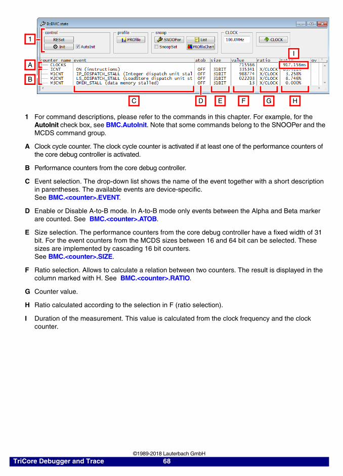
1 For command descriptions, please refer to the commands in this chapter. For example, for the AutoInit check box, see BMC.AutoInit. Note that some commands belong to the SNOOPer and the MCDS command group.
A Clock cycle counter. The clock cycle counter is activated if at least one of the performance counters of the core debug controller is activated.
B Performance counters from the core debug controller.
C Event selection. The drop-down list shows the name of the event together with a short description in parentheses. The available events are device-specific. See BMC.<counter>.EVENT.
D Enable or Disable A-to-B mode. In A-to-B mode only events between the Alpha and Beta marker are counted. See BMC.<counter>.ATOB.
E Size selection. The performance counters from the core debug controller have a fixed width of 31 bit. For the event counters from the MCDS sizes between 16 and 64 bit can be selected. These sizes are implemented by cascading 16 bit counters.See BMC.<counter>.SIZE.
F Ratio selection. Allows to calculate a relation between two counters. The result is displayed in the column marked with H. See BMC.<counter>.RATIO.
G Counter value.
H Ratio calculated according to the selection in F (ratio selection).
I Duration of the measurement. This value is calculated from the clock frequency and the clock counter.
C ED F G H
I
B
A
1
TriCore Debugger and Trace 68 ©1989-2018 Lauterbach GmbH
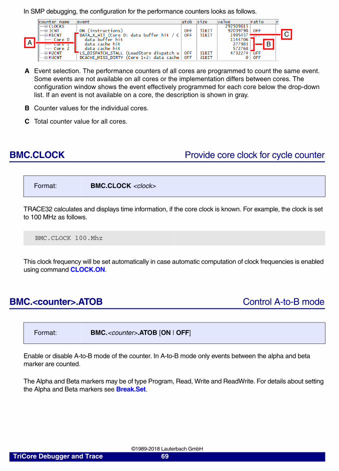
In SMP debugging, the configuration for the performance counters looks as follows.
BMC.CLOCK Provide core clock for cycle counter
TRACE32 calculates and displays time information, if the core clock is known. For example, the clock is set to 100 MHz as follows.
This clock frequency will be set automatically in case automatic computation of clock frequencies is enabled using command CLOCK.ON.
BMC.<counter>.ATOB Control A-to-B mode
Enable or disable A-to-B mode of the counter. In A-to-B mode only events between the alpha and beta marker are counted.
The Alpha and Beta markers may be of type Program, Read, Write and ReadWrite. For details about setting the Alpha and Beta markers see Break.Set.
A Event selection. The performance counters of all cores are programmed to count the same event. Some events are not available on all cores or the implementation differs between cores. The configuration window shows the event effectively programmed for each core below the drop-down list. If an event is not available on a core, the description is shown in gray.
B Counter values for the individual cores.
C Total counter value for all cores.
Format: BMC.CLOCK <clock>
BMC.CLOCK 100.Mhz
Format: BMC.<counter>.ATOB [ON | OFF]
AC
B
TriCore Debugger and Trace 69 ©1989-2018 Lauterbach GmbH
About the SYStem.CONFIG Commands
The SYStem.CONFIG commands are used to configure the behavior of the complete target system for debugging, e.g., the debug interface or the chaining of several CPUs.
SYStem.CONFIG.state Display target configuration
Opens the SYStem.CONFIG.state window, where you can view and modify most of the target configuration settings. The configuration settings tell the debugger how to communicate with the chip on the target board and how to access the on-chip debug and trace facilities in order to accomplish the debugger’s operations.
Alternatively, you can modify the target configuration settings via the TRACE32 command line with the SYStem.CONFIG commands. Note that the command line provides additional SYStem.CONFIG commands for settings that are not included in the SYStem.CONFIG.state window.
Format: SYStem.CONFIG.state [/<tab>]
<tab>: DebugPort | Jtag | XCP
<tab> Opens the SYStem.CONFIG.state window on the specified tab:DebugPort, JTAG, and XCP.
DebugPort Lets you configure the electrical properties of the debug connection, such as the communication protocol or the used pinout.
Jtag Informs the debugger about the position of the Test Access Ports (TAP) in the JTAG chain which the debugger needs to talk to in order to access the debug and trace facilities on the chip.
XCP Lets you configure the XCP connection to your target.
For descriptions of the commands on the XCP tab, see “XCP Debug Back-End” (backend_xcp.pdf).
TriCore Debugger and Trace 70 ©1989-2018 Lauterbach GmbH
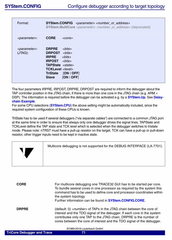
SYStem.CONFIG Configure debugger according to target topology
The four parameters IRPRE, IRPOST, DRPRE, DRPOST are required to inform the debugger about the TAP controller position in the JTAG chain, if there is more than one core in the JTAG chain (e.g. ARM + DSP). The information is required before the debugger can be activated e.g. by a SYStem.Up. See Daisy-chain Example.For some CPU selections (SYStem.CPU) the above setting might be automatically included, since the required system configuration of these CPUs is known.
TriState has to be used if several debuggers (“via separate cables”) are connected to a common JTAG port at the same time in order to ensure that always only one debugger drives the signal lines. TAPState and TCKLevel define the TAP state and TCK level which is selected when the debugger switches to tristate mode. Please note: nTRST must have a pull-up resistor on the target, TCK can have a pull-up or pull-down resistor, other trigger inputs need to be kept in inactive state.
Format: SYStem.CONFIG <parameter> <number_or_address>SYStem.MultiCore <parameter> <number_or_address> (deprecated)
<parameter>: CORE <core>
<parameter>:(JTAG):
DRPRE <bits>DRPOST <bits>IRPRE <bits>IRPOST <bits>TAPState <state>TCKLevel <level>TriState [ON | OFF]Slave [ON | OFF]
Multicore debugging is not supported for the DEBUG INTERFACE (LA-7701).
CORE For multicore debugging one TRACE32 GUI has to be started per core. To bundle several cores in one processor as required by the system this command has to be used to define core and processor coordinates within the system topology.Further information can be found in SYStem.CONFIG.CORE.
DRPRE (default: 0) <number> of TAPs in the JTAG chain between the core of interest and the TDO signal of the debugger. If each core in the system contributes only one TAP to the JTAG chain, DRPRE is the number of cores between the core of interest and the TDO signal of the debugger.
TriCore Debugger and Trace 71 ©1989-2018 Lauterbach GmbH
DRPOST (default: 0) <number> of TAPs in the JTAG chain between the TDI signal of the debugger and the core of interest. If each core in the system contributes only one TAP to the JTAG chain, DRPOST is the number of cores between the TDI signal of the debugger and the core of interest.
IRPRE (default: 0) <number> of instruction register bits in the JTAG chain between the core of interest and the TDO signal of the debugger. This is the sum of the instruction register length of all TAPs between the core of interest and the TDO signal of the debugger.
IRPOST (default: 0) <number> of instruction register bits in the JTAG chain between the TDI signal and the core of interest. This is the sum of the instruction register lengths of all TAPs between the TDI signal of the debugger and the core of interest.
TAPState (default: 7 = Select-DR-Scan) This is the state of the TAP controller when the debugger switches to tristate mode. All states of the JTAG TAP controller are selectable.
TCKLevel (default: 0) Level of TCK signal when all debuggers are tristated.
TriState (default: OFF) If several debuggers share the same debug port, this option is required. The debugger switches to tristate mode after each debug port access. Then other debuggers can access the port. JTAG: This option must be used, if the JTAG line of multiple debug boxes are connected by a JTAG joiner adapter to access a single JTAG chain.
Slave (default: OFF) If more than one debugger share the same debug port, all except one must have this option active.JTAG: Only one debugger - the “master” - is allowed to control the signals nTRST and nSRST (nRESET).
TriCore Debugger and Trace 72 ©1989-2018 Lauterbach GmbH
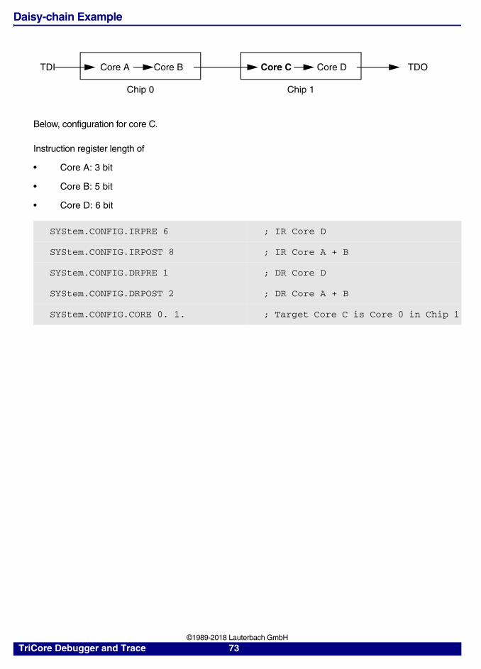
Daisy-chain Example
Below, configuration for core C.
Instruction register length of
• Core A: 3 bit
• Core B: 5 bit
• Core D: 6 bit
SYStem.CONFIG.IRPRE 6 ; IR Core D
SYStem.CONFIG.IRPOST 8 ; IR Core A + B
SYStem.CONFIG.DRPRE 1 ; DR Core D
SYStem.CONFIG.DRPOST 2 ; DR Core A + B
SYStem.CONFIG.CORE 0. 1. ; Target Core C is Core 0 in Chip 1
Core A Core B Core C Core D TDOTDI
Chip 0 Chip 1
TriCore Debugger and Trace 73 ©1989-2018 Lauterbach GmbH
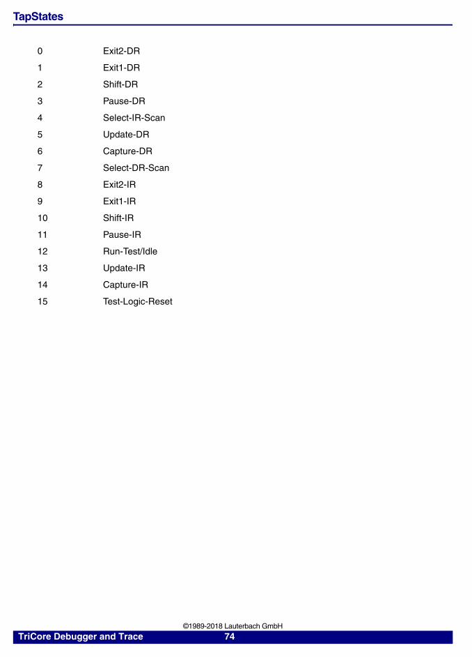
TapStates
0 Exit2-DR
1 Exit1-DR
2 Shift-DR
3 Pause-DR
4 Select-IR-Scan
5 Update-DR
6 Capture-DR
7 Select-DR-Scan
8 Exit2-IR
9 Exit1-IR
10 Shift-IR
11 Pause-IR
12 Run-Test/Idle
13 Update-IR
14 Capture-IR
15 Test-Logic-Reset
TriCore Debugger and Trace 74 ©1989-2018 Lauterbach GmbH
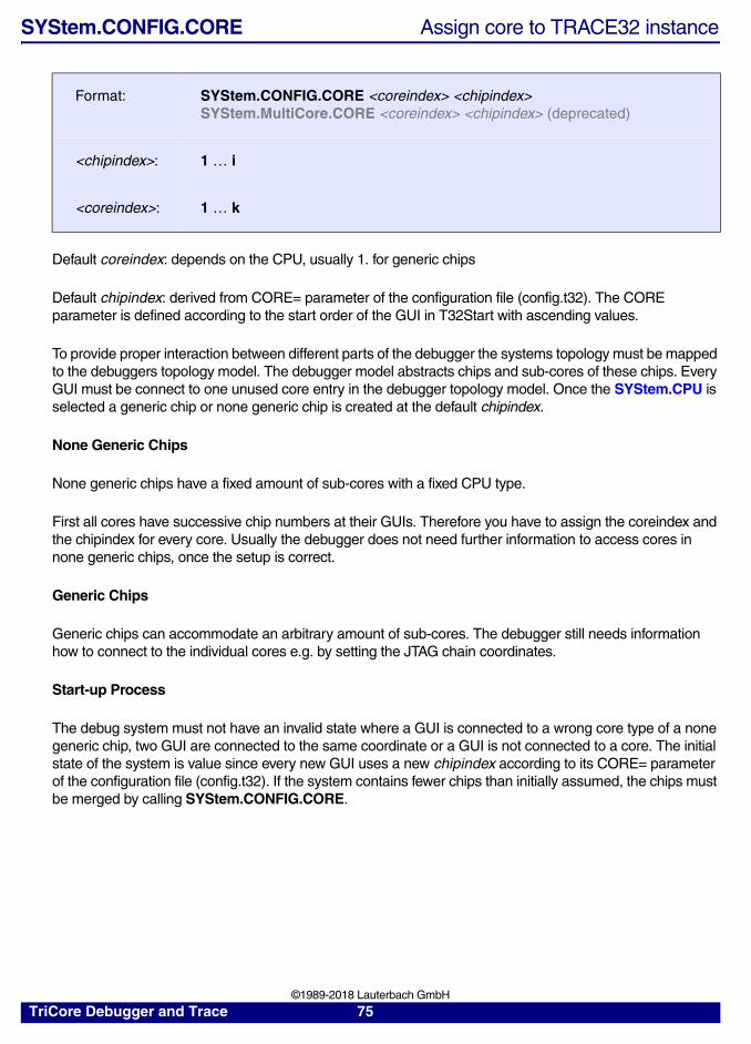
SYStem.CONFIG.CORE Assign core to TRACE32 instance
Default coreindex: depends on the CPU, usually 1. for generic chips
Default chipindex: derived from CORE= parameter of the configuration file (config.t32). The CORE parameter is defined according to the start order of the GUI in T32Start with ascending values.
To provide proper interaction between different parts of the debugger the systems topology must be mapped to the debuggers topology model. The debugger model abstracts chips and sub-cores of these chips. Every GUI must be connect to one unused core entry in the debugger topology model. Once the SYStem.CPU is selected a generic chip or none generic chip is created at the default chipindex.
None Generic Chips
None generic chips have a fixed amount of sub-cores with a fixed CPU type.
First all cores have successive chip numbers at their GUIs. Therefore you have to assign the coreindex and the chipindex for every core. Usually the debugger does not need further information to access cores in none generic chips, once the setup is correct.
Generic Chips
Generic chips can accommodate an arbitrary amount of sub-cores. The debugger still needs information how to connect to the individual cores e.g. by setting the JTAG chain coordinates.
Start-up Process
The debug system must not have an invalid state where a GUI is connected to a wrong core type of a none generic chip, two GUI are connected to the same coordinate or a GUI is not connected to a core. The initial state of the system is value since every new GUI uses a new chipindex according to its CORE= parameter of the configuration file (config.t32). If the system contains fewer chips than initially assumed, the chips must be merged by calling SYStem.CONFIG.CORE.
Format: SYStem.CONFIG.CORE <coreindex> <chipindex>SYStem.MultiCore.CORE <coreindex> <chipindex> (deprecated)
<chipindex>: 1 … i
<coreindex>: 1 … k
TriCore Debugger and Trace 75 ©1989-2018 Lauterbach GmbH
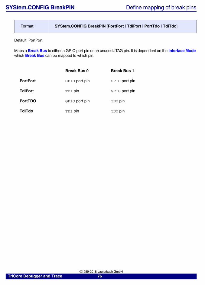
SYStem.CONFIG BreakPIN Define mapping of break pins
Default: PortPort.
Maps a Break Bus to either a GPIO port pin or an unused JTAG pin. It is dependent on the Interface Mode which Break Bus can be mapped to which pin:
Format: SYStem.CONFIG BreakPIN [PortPort | TdiPort | PortTdo | TdiTdo]
Break Bus 0 Break Bus 1
PortPort GPIO port pin GPIO port pin
TdiPort TDI pin GPIO port pin
PortTDO GPIO port pin TDO pin
TdiTdo TDI pin TDO pin
TriCore Debugger and Trace 76 ©1989-2018 Lauterbach GmbH
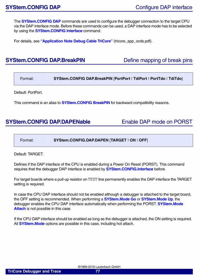
SYStem.CONFIG DAP Configure DAP interface
The SYStem.CONFIG DAP commands are used to configure the debugger connection to the target CPU via the DAP interface mode. Before these commands can be used, a DAP interface mode has to be selected by using the SYStem.CONFIG Interface command.
For details, see “Application Note Debug Cable TriCore” (tricore_app_ocds.pdf).
SYStem.CONFIG DAP.BreakPIN Define mapping of break pins
Default: PortPort.
This command is an alias to SYStem.CONFIG BreakPIN for backward compatibility reasons.
SYStem.CONFIG DAP.DAPENable Enable DAP mode on PORST
Default: TARGET.
Defines if the DAP interface of the CPU is enabled during a Power On Reset (PORST). This command requires that the debugger DAP interface is enabled by SYStem.CONFIG.Interface before.
For target boards where a pull-up resistor on TRST line permanently enables the DAP interface the TARGET setting is required.
In case the CPU DAP interface should not be enabled although a debugger is attached to the target board, the OFF setting is recommended. When performing a SYStem.Mode Go or SYStem.Mode Up, the debugger enables the CPU DAP interface automatically when performing the PORST. SYStem.Mode Attach is not possible in this case.
If the CPU DAP interface should be enabled as long as the debugger is attached, the ON setting is required. All SYStem.Mode options are possible in this case, including hot attach.
Format: SYStem.CONFIG DAP.BreakPIN [PortPort | TdiPort | PortTdo | TdiTdo]
Format: SYStem.CONFIG.DAP.DAPEN [TARGET | ON | OFF]
TriCore Debugger and Trace 77 ©1989-2018 Lauterbach GmbH
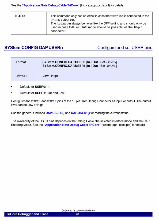
See the “Application Note Debug Cable TriCore” (tricore_app_ocds.pdf) for details.
SYStem.CONFIG DAP.USERn Configure and set USER pins
• Default for USER0: In.
• Default for USER1: Out and Low.
Configures the USER0 and USER1 pins of the 10 pin DAP Debug Connector as input or output. The output level can be Low or High.
Use the general functions DAP.USER0() and DAP.USER1() for reading the current status.
The availability of the USER pins depends on the Debug Cable, the selected interface mode and the DAP Enabling Mode. See the “Application Note Debug Cable TriCore” (tricore_app_ocds.pdf) for details.
NOTE: This command only has an effect in case the TRST line is connected to the DAPEN output pin. The ALTEN pin always behaves like the OFF setting and should only be used in case DAP or JTAG mode should be possible via the 16-pin connector.
Format: SYStem.CONFIG.DAP.USER0 [In | Out | Set <level>]SYStem.CONFIG.DAP.USER1 [In | Out | Set <level>]
<level>: Low | High
TriCore Debugger and Trace 78 ©1989-2018 Lauterbach GmbH
SYStem.CONFIG.DEBUGPORT Select target interface
Selects the interface to the target. The available options depend on whether TRACE32 uses a hardware debugger or runs in HostMCI mode (without TRACE32 hardware).
With TRACE32 hardware
HostMCI mode
SYStem.CONFIG.DEBUGPORTTYPE Set debug cable interface mode
Default: DAP2 (JTAG).
Configures the debug port type to be used by the debugger. Both CPU and Debug Cable must support this mode, see “Application Note Debug Cable TriCore” (tricore_app_ocds.pdf) for details.
As of build 92378 - DVD 02/2018, the default is DAP2, unless the Debug Cable or CPU do not support this mode.
DAP3: Supported for AURIX only.
Format: SYStem.CONFIG.DEBUGPORT <port>
<port>: DebugCable0 | DebugCableA | InfineonDAS0 | XCP0 | Unknown
DebugCable0 Uses the debug cable directly connected to a PowerDebug module.
DebugCableA Uses the whisker connected to a CombiProbe.
InfineonDAS0 Selects the Infineon DAS backend. For a detailed description and examples, see “Debugging via Infineon DAS Server” (backend_das.pdf).
XCP0 Select the XCP backend. For a detailed description and examples, see “XCP Debug Back-End” (backend_xcp.pdf).
Unknown No backend is selected. Debugging is not possible.
Format: SYStem.CONFIG.DEBUGPORTTYPE [JTAG | DAP2 | DAP3 | DXCPL]SYStem.CONFIG.Interface [JTAG | DAP2] (deprecated)
TriCore Debugger and Trace 79 ©1989-2018 Lauterbach GmbH
SYStem.CONFIG DXCPL Configure DXCPL
The abbreviation DXCPL stands for DAP over CAN Physical Layer by Infineon.
SYStem.CONFIG DXCPL.Timing Configure SPD timing for DXCPL
Default: AUTO.
Configures the edge distance for a ‘0’ bit.
• For AURIX device about 0.80µs recommended.
• For AUDO MAX device it depends on the crystal which is used for the clock. 0.50µs for a 20MHz crystal and 1.00µs for a 10MHz crystal.
SYStem.CONFIG.EXTWDTDIS Disable external watchdog
Controls the WDTDIS pin of the Automotive Debug Cable. This option is only available if an Automotive Debug Cable is connected to the PowerDebug module.
See also “Application Note Debug Cable TriCore” (tricore_app_ocds.pdf).
Format: SYStem.CONFIG DXCPL.Timing [AUTO | <time>]
AUTO The option AUTO checks the working timing settings and prints it in the AREA.view window. AUTO should only used with SYStem.Mode Attach.
Format: SYStem.CONFIG EXTWDTDIS <option>
<option>: HighLow
High The WDTDIS pin is permanently driven high (default).
Low The WDTDIS pin is permanently driven low.
TriCore Debugger and Trace 80 ©1989-2018 Lauterbach GmbH
SYStem.CONFIG PortSHaRing Control sharing of debug port with other tool
Configure if the debug port is shared with another tool, e.g., an ETAS ETK.
The current setting can be obtained by the PORTSHARING() function, immediate detection can be performed using SYStem.DETECT PortSHaRing.
See also “Parallel Usage of a 3rd-Party Tool”, page 41.
SYStem.CPU Select CPU
Default: TC1797.
Selects the processor type.
Format: SYStem.CONFIG PortSHaRing [ON | OFF | Auto]
ON Request for access to the debug port and wait until the access is granted before communicating with the target.
OFF Communicate with the target without sending requests.
Auto Automatically detect a connected tool on next SYStem.Mode Up, SYStem.Mode Attach or SYStem.Mode Go. If a tool is detected switch to mode ON else switch to mode OFF.
Format: SYStem.CPU <cpu>
<cpu> For a list of supported CPUs, use the command SYStem.CPU * or refer to the chip search on the Lauterbach website.
NOTE: In case your device is listed on the website but not listed in the SYStem.CPU * list, you may require a software update. Please contact your responsible Lauterbach representative.
TriCore Debugger and Trace 81 ©1989-2018 Lauterbach GmbH
SYStem.CpuAccess Run-time CPU access (intrusive)
Default: Denied.
This option declares if an intrusive memory access can take place while the CPU is executing code. To perform this access, the debugger stops the CPU shortly, performs the access and then restarts the CPU.
The run-time memory access has to be activated for each window by using the memory class E: (e.g. Data.dump ED:0xA1000000) or by using the format option %E (e.g. Var.View %E var1).
SYStem.JtagClock Set the JTAG frequency
Default: 10 MHz.
Format: SYStem.CpuAccess <mode>
<mode>: Enable | Denied | Nonstop
Enable Stop the CPU shortly to perform a memory read or write while the program execution is running.Each short stop takes 1 … 100 ms depending on the speed of the debug interface and on the size of the read/write accesses required.
Denied No intrusive memory read or write is possible while the CPU is executing the program.
Nonstop The program execution cannot be stopped and the real-time behavior of the CPU is not affected.Nonstop reduces the functionality of the debugger to:• Run-time access to memory and variables• Trace displayThe debugger inhibits the following:• To stop the program execution• All features of the debugger that are intrusive (e.g. spot break-
points, performance analysis via StopAndGo, conditional break-points etc.)
Format: SYStem.JtagClock <rate>SYStem.BdmClock (deprecated)
<rate>: 10000. … 50000000.
TriCore Debugger and Trace 82 ©1989-2018 Lauterbach GmbH
Selects the frequency for the JTAG clock. This influences the speed of data transmission between target and debugger.
Not all values in between the frequency range can be generated by the debugger. The debugger will select and display the possible value if it cannot generate the exact value.It is also possible to enter units, e.g. 10.0 MHz.
SYStem.JtagClock EXT is not supported by TriCore.
SYStem.LOCK Tristate the JTAG port
Default: OFF.
If the system is locked no access to the JTAG port will be performed by the debugger. While locked the JTAG connector of the debugger is tristated. The intention of the lock command is for example to give JTAG access to another tool. The process can also be automated, see SYStem.CONFIG TriState.
NOTE: The JTAG clock must be lower or equal to the CPU clock. Otherwise JTAG communication will fail.The possible maximum of the JTAG clock is extremely dependent of the target board layout.
Format: SYStem.LOCK [ON | OFF]
TriCore Debugger and Trace 83 ©1989-2018 Lauterbach GmbH
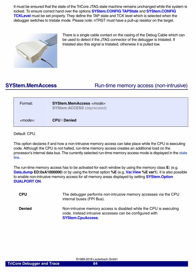
It must be ensured that the state of the TriCore JTAG state machine remains unchanged while the system is locked. To ensure correct hand over the options SYStem.CONFIG TAPState and SYStem.CONFIG TCKLevel must be set properly. They define the TAP state and TCK level which is selected when the debugger switches to tristate mode. Please note: nTRST must have a pull-up resistor on the target.
SYStem.MemAccess Run-time memory access (non-intrusive)
Default: CPU.
This option declares if and how a non-intrusive memory access can take place while the CPU is executing code. Although the CPU is not halted, run-time memory access creates an additional load on the processor’s internal data bus. The currently selected run-time memory access mode is displayed in the state line.
The run-time memory access has to be activated for each window by using the memory class E: (e.g. Data.dump ED:0xA1000000) or by using the format option %E (e.g. Var.View %E var1). It is also possible to enable non-intrusive memory access for all memory areas displayed by setting SYStem.Option DUALPORT ON.
There is a single cable contact on the casing of the Debug Cable which can be used to detect if the JTAG connector of the debugger is tristated. If tristated also this signal is tristated, otherwise it is pulled low.
Format: SYStem.MemAccess <mode> SYStem.ACCESS (deprecated)
<mode>: CPU | Denied
CPU The debugger performs non-intrusive memory accesses via the CPU internal buses (FPI Bus).
Denied Non-intrusive memory access is disabled while the CPU is executing code. Instead intrusive accesses can be configured with SYStem.CpuAccess.
TriCore Debugger and Trace 84 ©1989-2018 Lauterbach GmbH
SYStem.Mode Establish the communication with the CPU
Initial mode: Down.
The SYStem modes are not only commands to bring the debugger in a certain debug state, they also reflect the current debug state of the target. SYStem.Mode Attach and SYStem.Mode Go are only transitional states which will result in an Up state on success. Any critical failure will transition the debug state to SYStem.Mode Down immediately.
The “Emulate” LED on the debug module is ON when the debug mode is active and the CPU is running.
Format: SYStem.Mode <mode>
<mode>: DownNoDebugPrepareGoAttachUpStandBy
Down Default state and state after fatal errors. The behavior can be configured with SYStem.Option DOWNMODE.
NoDebug The CPU is running. Debug mode is not active, debug port is tristate. In this mode the target behaves as if the debugger is not connected.
Prepare Establishes connection to the target and resets the debug module. This debugging mode is used if no CPU shall be debugged.The mode allows to access memory and peripherals.
Attach User program remains running (no reset) and the debug mode is activated. After this command the user program can be stopped with the break command or if any break condition occurs. The debugger should be in NoDebug mode when performing an Attach.
Go The CPU is reset and starts executing user code. Debug mode is active. After this command the CPU can be stopped with the Break command or if any break condition occurs.
Up The CPU is reset and halted at the reset vector. Debug mode is active. In this mode the CPU can be started and stopped. This is the most common way to activate debugging.
StandBy Activates debugging through power cycles, see “Power Cycles”, page 47.
NOTE: For the SYStem.Mode Up the JTAG clock must be high enough. Otherwise the debugger is not able to configure the Halt-After-Reset before the on-chip startup firmware has completed. SYStem.JtagClock 500.0KHz or higher is a save value for all CPUs.
TriCore Debugger and Trace 85 ©1989-2018 Lauterbach GmbH
SYStem.Option CPU specific commands
The SYStem.Option commands are architecture and CPU specific commands.
SYStem.Option BREAKFIX Enable workaround for asynchronous breaking
Default: ON for all TriCore v1.3.1 cores, OFF otherwise.
This option is mainly used as a workaround for silicon bug OCDS_TC.028, where the functionality of the loop instruction may be corrupted by FPI accesses to the [0xF7E10000--0xF7E1FFFF] address region. The Debug Status Register (DBGSR), used for asynchronous breaking, resides in this region.
Switching the SYStem.Option BREAKFIX ON will temporarily suspend the TriCore when breaking to allow safe accesses to the critical region. The break is then issued by configuring the Memory Protection System of the TriCore.
Format: SYStem.Option BREAKFIX [ON | OFF]
TriCore Debugger and Trace 86 ©1989-2018 Lauterbach GmbH
SYStem.Option CBSACCEN<x> Cerberus access protection
Default: CerBeruS.
Handles the behavior of TRACE32 with respect to the CBS_ACCEN<x> registers of the Cerberus block.
The <value> is the OR-composition of the following:
Example 1: Do not touch the CBS_ACCEN0 register.
Example 2: Enable access from the debugger to the Cerberus block.
Example 3: Enable access from the debugger and two more masters (described by <mask>) to the Cerberus block. The two syntax examples are equivalent:
Format: SYStem.Option CBSACCEN<x> TarGeT | <value>
<x>: 0
<value>: CerBeruS | <mask> [CerBeruS | <mask>] …
TarGeT TRACE32 will not touch the specified CBS_ACCEN<x> register.
<value> The value is written to the register when the core is started.
CerBeruS Access for the debugger.
<mask> Arbitrary mask. For valid masks, refer to the TriCore User Manual.
SYStem.Option CBSACCEN0 TarGeT
SYStem.Option CBSACCEN0 CerBeruS
; |---------- <value> -----------|; <mask> <mask>SYStem.Option CBSACCEn0 CerBeruS 0x000000001 0x00000002
; |---------- <value> -----------|; <mask> <mask>SYStem.Option CBSACCEn0 0x000000001 CerBeruS 0x00000002
TriCore Debugger and Trace 87 ©1989-2018 Lauterbach GmbH

SYStem.Option DCFREEZE Do not invalidate cache
Default: ON.
If enabled the data cache contents will not be touched on write accesses. If disabled, cache lines may be invalidated/flushed on write accesses.
SYStem.Option DCREAD Read from data cache
Default: OFF.
If disabled, physical memory is accessed directly (as seen from the bus).
If enabled, memory accesses with access class D: (data) and variable windows display the memory values from the data cache, if valid. If data is not available in cache, physical memory will be read. Memory will be seen as from the CPU’s point of view.
TriCore cores do not allow cache access during CPU runtime. All accesses will be automatically redirected to physical memory when the CPU is running, given that run-time memory access is enabled (e.g. with SYStem.Option DUALPORT). The following table illustrates the effect.
More information is available in chapter “Cache Access”, page 39.
Format: SYStem.Option DCFREEZE [ON | OFF]
Format: SYStem.Option DCREAD [ON | OFF]
DCREAD CPU is Read Access class D: is like
ON stopped through data cache DC:
ON running physical memory NC:
OFF stopped or running physical memory NC:
TriCore Debugger and Trace 88 ©1989-2018 Lauterbach GmbH
SYStem.Option DOWNMODE Behavior of SYStem.Mode Down
Configures the behavior of SYStem.Mode Down:
SYStem.Option DUALPORT Run-time memory access for all windows
Default: OFF.
Enables permanent non-intrusive memory access for all windows and memory accesses. Memory access class E: does not have to be specified any more. In other words, memory can be accessed while the CPU is running.
This only works when SYStem.MemAccess is set to CPU. For details, see chapter “Run-time Memory Access” in TRACE32 Glossary, page 30 (glossary.pdf).
SYStem.Option DataTrace Enable data tracingOCDS-L2 trace only
Default is OFF.
The CPU trace port does not support data tracing. This option uses code instrumentation to output some data. See the example in ~~/demo/tricore/etc/tracedata/ in your demo directory for more information on how to modify your application.
Format: SYStem.Option DOWNMODE TriState | ReSeT
TriState (default) All drivers of the debug port are switched off.
ReSeT The CPU is held in reset.
Format: SYStem.Option DUALPORT [ON | OFF]
NOTE: When this option is enabled, then do not open Data.dump or Data.List windows while programming the on-chip flash. Otherwise flash operation will fail.
Format: SYStem.Option DataTrace [ON | OFF]
TriCore Debugger and Trace 89 ©1989-2018 Lauterbach GmbH
This is not a real data trace since it doesn’t trace the buses. But it may be enough to output some RTOS related information as thread IDs or task IDs.
For transferring more data, you may want to use the FDX command group, for a real bus trace, you may want to use the on-chip tracing features of the Emulation Devices (TC17xxED).
SYStem.Option ETK Debugging together with ETK from ETAS
SYStem.Option HeartBeat Bug fix to avoid FPI bus conflict
Default: OFF.
This option should be used as a workaround for the FPI bus problem on RiderA and AudoLite only. Otherwise bus errors occur when the debugger checks if the processor is running by reading a core special function register via FPI bus. With this option active there are two additional conditions checked first before any read via FPI bus will be done by the debugger. If one of these conditions is true, it is assumed that the processor is still running.
If a RiscTrace is used together with the debugger, the debugger first checks if the RiscTrace is still recording. The RiscTrace may not be used in stack mode.
If a RiscTrace is not used or stack mode is required, the debugger checks if pin 15 (reserved) of the JTAG connector will be toggled. If toggled it is assumed that the processor is running. Therefore it is required to connect a signal there, which will be toggled while the processor is running. A good signal would be the ORed signal of the pipeline status information EMUSTAT0-4 which are available on the OCDS Level 2 connector pin 4-8. Please note that on AudoLite these pins must be activated byData.Set 0xF0003748 %Long 0xFFFFFFFF.The connection of one of these pipeline status information lines (e.g. pin 6) might be sufficient. The signal high level must be lower or equal than VCCS (Pin 2 of JTAG connector) and at least 2.0 V. The signal low level must be lower than 0.8 V. The switching frequency should be higher than 10 Hz.
To avoid other FPI bus conflicts, do not use SYStem.Option DUALPORT and do not use the access class attribute E.
Format: SYStem.Option ETK [ON | AUTO | OFF] (deprecated)Use SYStem.CONFIG PortSHaRing instead.
Format: SYStem.Option HeartBeat [ON | OFF]
NOTE: RiderA and AudoLite are not supported any more, so this feature is obsolete.
TriCore Debugger and Trace 90 ©1989-2018 Lauterbach GmbH
SYStem.Option ICFLUSH Flush instruction cache at "Go" or "Step"
Default: ON.
If enabled, an instruction cache flush will be performed with each Go or Step. This is especially required if software breakpoints are used.
AURIX TC1.6P cores are unable to flush the instruction cache while the core is halted. Thus, flushing will be performed as soon as the core switches to running state. During flush sequence accesses to cacheable memory will stall the CPU, which can result in a slight asynchronity in a multicore system.
Newer AUDO-Future TriCore derivatives (TC11xx, TC1762, TC1764, TC1766, TC1766ED, TC1792, TC1796 and TC1796ED) have a silicon bug which prevents the line buffer cache to be invalidated during CPU halt. See the demo scripts for a workaround.
SYStem.Option IMASKASM Disable interrupts while single stepping
Default: OFF.
If enabled, the interrupt mask bits of the CPU will be set during assembler single-step operations. The interrupt routine is not executed during single-step operations. After single step the interrupt mask bits are restored to the value before the step.
On AUDO-Future devices, IMASKASM might not always work due to chip bug CPU_TC.115 (see the corresponding Infineon Errata sheets). Enable SYStem.Option STEPONCHIP concurrently as a workaround.
SYStem.Option IMASKHLL Disable interrupts while HLL single stepping
Default: OFF.
If enabled, the interrupt mask bits of the CPU will be set during HLL single-step operations. The interrupt routine is not executed during single-step operations. After single step the interrupt mask bits are restored to the value before the step.
Format: SYStem.Option ICFLUSH [ON | OFF]
Format: SYStem.Option IMASKASM [ON | OFF]
Format: SYStem.Option IMASKHLL [ON | OFF]
TriCore Debugger and Trace 91 ©1989-2018 Lauterbach GmbH
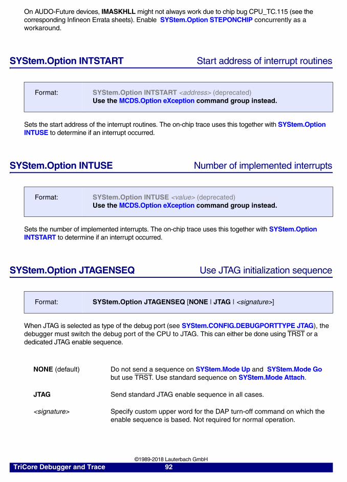
On AUDO-Future devices, IMASKHLL might not always work due to chip bug CPU_TC.115 (see the corresponding Infineon Errata sheets). Enable SYStem.Option STEPONCHIP concurrently as a workaround.
SYStem.Option INTSTART Start address of interrupt routines
Sets the start address of the interrupt routines. The on-chip trace uses this together with SYStem.Option INTUSE to determine if an interrupt occurred.
SYStem.Option INTUSE Number of implemented interrupts
Sets the number of implemented interrupts. The on-chip trace uses this together with SYStem.Option INTSTART to determine if an interrupt occurred.
SYStem.Option JTAGENSEQ Use JTAG initialization sequence
When JTAG is selected as type of the debug port (see SYStem.CONFIG.DEBUGPORTTYPE JTAG), the debugger must switch the debug port of the CPU to JTAG. This can either be done using TRST or a dedicated JTAG enable sequence.
Format: SYStem.Option INTSTART <address> (deprecated)Use the MCDS.Option eXception command group instead.
Format: SYStem.Option INTUSE <value> (deprecated)Use the MCDS.Option eXception command group instead.
Format: SYStem.Option JTAGENSEQ [NONE | JTAG | <signature>]
NONE (default) Do not send a sequence on SYStem.Mode Up and SYStem.Mode Go but use TRST. Use standard sequence on SYStem.Mode Attach.
JTAG Send standard JTAG enable sequence in all cases.
<signature> Specify custom upper word for the DAP turn-off command on which the enable sequence is based. Not required for normal operation.
TriCore Debugger and Trace 92 ©1989-2018 Lauterbach GmbH
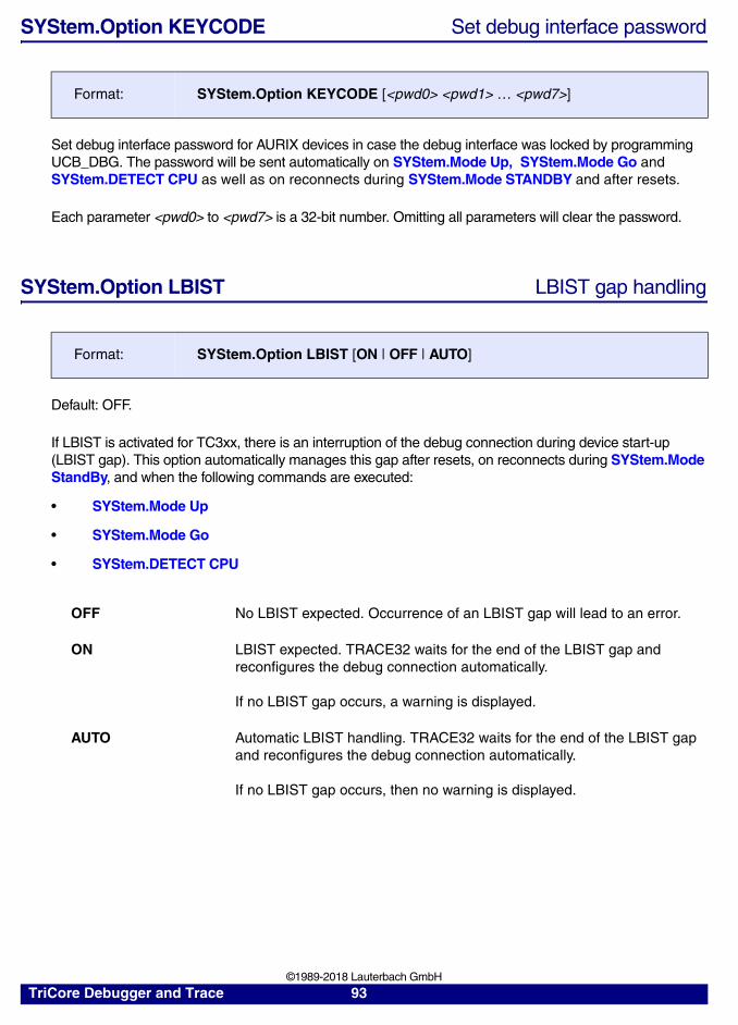
SYStem.Option KEYCODE Set debug interface password
Set debug interface password for AURIX devices in case the debug interface was locked by programming UCB_DBG. The password will be sent automatically on SYStem.Mode Up, SYStem.Mode Go and SYStem.DETECT CPU as well as on reconnects during SYStem.Mode STANDBY and after resets.
Each parameter <pwd0> to <pwd7> is a 32-bit number. Omitting all parameters will clear the password.
SYStem.Option LBIST LBIST gap handling
Default: OFF.
If LBIST is activated for TC3xx, there is an interruption of the debug connection during device start-up (LBIST gap). This option automatically manages this gap after resets, on reconnects during SYStem.Mode StandBy, and when the following commands are executed:
• SYStem.Mode Up
• SYStem.Mode Go
• SYStem.DETECT CPU
Format: SYStem.Option KEYCODE [<pwd0> <pwd1> … <pwd7>]
Format: SYStem.Option LBIST [ON | OFF | AUTO]
OFF No LBIST expected. Occurrence of an LBIST gap will lead to an error.
ON LBIST expected. TRACE32 waits for the end of the LBIST gap and reconfigures the debug connection automatically.
If no LBIST gap occurs, a warning is displayed.
AUTO Automatic LBIST handling. TRACE32 waits for the end of the LBIST gap and reconfigures the debug connection automatically.
If no LBIST gap occurs, then no warning is displayed.
TriCore Debugger and Trace 93 ©1989-2018 Lauterbach GmbH
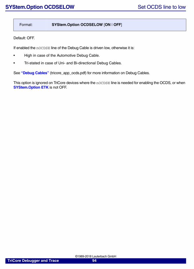
SYStem.Option OCDSELOW Set OCDS line to low
Default: OFF.
If enabled the nOCDSE line of the Debug Cable is driven low, otherwise it is:
• High in case of the Automotive Debug Cable.
• Tri-stated in case of Uni- and Bi-directional Debug Cables.
See “Debug Cables” (tricore_app_ocds.pdf) for more information on Debug Cables.
This option is ignored on TriCore devices where the nOCDSE line is needed for enabling the OCDS, or when SYStem.Option ETK is not OFF.
Format: SYStem.Option OCDSELOW [ON | OFF]
TriCore Debugger and Trace 94 ©1989-2018 Lauterbach GmbH
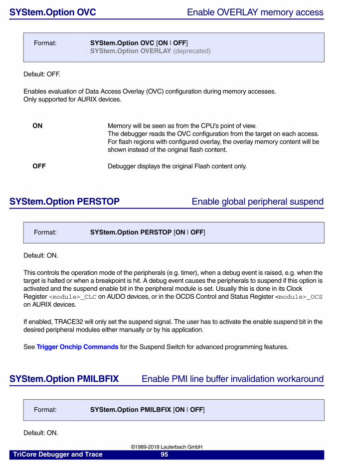
SYStem.Option OVC Enable OVERLAY memory access
Default: OFF.
Enables evaluation of Data Access Overlay (OVC) configuration during memory accesses.Only supported for AURIX devices.
SYStem.Option PERSTOP Enable global peripheral suspend
Default: ON.
This controls the operation mode of the peripherals (e.g. timer), when a debug event is raised, e.g. when the target is halted or when a breakpoint is hit. A debug event causes the peripherals to suspend if this option is activated and the suspend enable bit in the peripheral module is set. Usually this is done in its Clock Register <module>_CLC on AUDO devices, or in the OCDS Control and Status Register <module>_OCS on AURIX devices.
If enabled, TRACE32 will only set the suspend signal. The user has to activate the enable suspend bit in the desired peripheral modules either manually or by his application.
See Trigger Onchip Commands for the Suspend Switch for advanced programming features.
SYStem.Option PMILBFIX Enable PMI line buffer invalidation workaround
Default: ON.
Format: SYStem.Option OVC [ON | OFF]SYStem.Option OVERLAY (deprecated)
ON Memory will be seen as from the CPU’s point of view.The debugger reads the OVC configuration from the target on each access. For flash regions with configured overlay, the overlay memory content will be shown instead of the original flash content.
OFF Debugger displays the original Flash content only.
Format: SYStem.Option PERSTOP [ON | OFF]
Format: SYStem.Option PMILBFIX [ON | OFF]
TriCore Debugger and Trace 95 ©1989-2018 Lauterbach GmbH
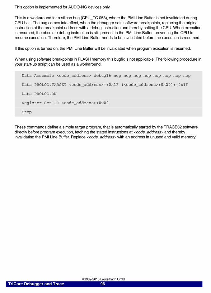
This option is implemented for AUDO-NG devices only.
This is a workaround for a silicon bug (CPU_TC.053), where the PMI Line Buffer is not invalidated during CPU halt. The bug comes into effect, when the debugger sets software breakpoints, replacing the original instruction at the breakpoint address with a debug instruction and thereby halting the CPU. When execution is resumed, the obsolete debug instruction is still present in the PMI Line Buffer, preventing the CPU to resume execution. Therefore, the PMI Line Buffer needs to be invalidated before the execution is resumed.
If this option is turned on, the PMI Line Buffer will be invalidated when program execution is resumed.
When using software breakpoints in FLASH memory this bugfix is not applicable. The following procedure in your start-up script can be used as a workaround.
These commands define a simple target program, that is automatically started by the TRACE32 software directly before program execution, fetching the stated instructions at <code_address> and thereby invalidating the PMI Line Buffer. Replace <code_address> with an address in unused and valid memory.
Data.Assemble <code_address> debug16 nop nop nop nop nop nop nop nop
Data.PROLOG.TARGET <code_address>++0x1F (<code_address>+0x20)++0x1F
Data.PROLOG.ON
Register.Set PC <code_address>+0x02
Step
TriCore Debugger and Trace 96 ©1989-2018 Lauterbach GmbH
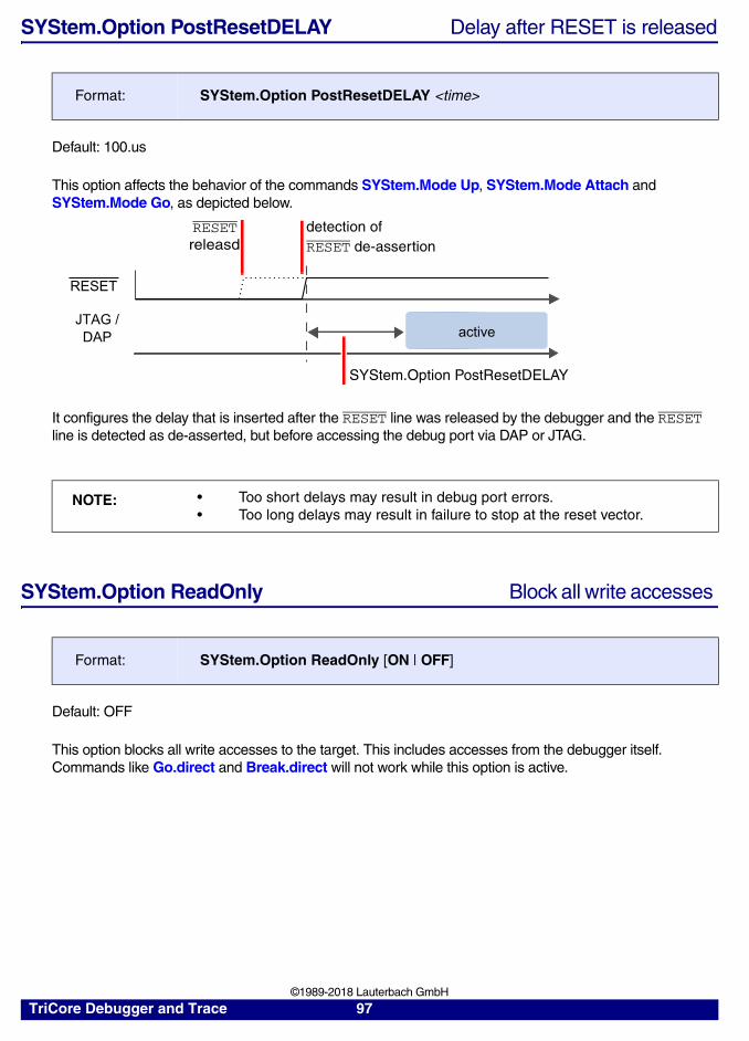
SYStem.Option PostResetDELAY Delay after RESET is released
Default: 100.us
This option affects the behavior of the commands SYStem.Mode Up, SYStem.Mode Attach and SYStem.Mode Go, as depicted below.
It configures the delay that is inserted after the RESET line was released by the debugger and the RESET line is detected as de-asserted, but before accessing the debug port via DAP or JTAG.
SYStem.Option ReadOnly Block all write accesses
Default: OFF
This option blocks all write accesses to the target. This includes accesses from the debugger itself. Commands like Go.direct and Break.direct will not work while this option is active.
Format: SYStem.Option PostResetDELAY <time>
NOTE: • Too short delays may result in debug port errors.• Too long delays may result in failure to stop at the reset vector.
Format: SYStem.Option ReadOnly [ON | OFF]
JTAG /DAP
RESET
active
RESET detection ofRESET de-assertion releasd
SYStem.Option PostResetDELAY
TriCore Debugger and Trace 97 ©1989-2018 Lauterbach GmbH
SYStem.Option RESetBehavior Set behavior when a reset occurs
Sets the behavior in case of a reset. For a detailed explanation, see Debugging through Resets.
SYStem.Option ResetDetection Set how hard resets are detected
Configure which of the following methods TRACE32 uses to detect hard resets.
Format: SYStem.Option RESetBehavior <mode>
<mode>: HaltRestoreGoRunRestore
Halt Halt after reset.
RestoreGo Halt after power-on reset, restore the debugging resources (e.g., breakpoints), and then go. After a soft reset, the debugger does not stop the CPU. The debugging resources remain in place.
RunRestore Restore debugging resources after power-on reset while CPU is running. Breakpoints shortly after a reset will be missed. After a soft reset, the debugger does not stop the CPU. The debugging resources remain in place.
Format: SYStem.Option ResetDetection <mode>
<mode>: DEFaultTIMEOUT
DEFault A hard reset is detected on a low pulse of the RESET line or a time out of the debug connection.
TIMEOUT A hard reset is detected on a time out of the debug connection only.
TriCore Debugger and Trace 98 ©1989-2018 Lauterbach GmbH
SYStem.Option RESetTMS State of TMS line at reset
Default: OFF.
Configures the state of the TMS line at the time the RESET line is released by commands SYStem.Mode Up and SYStem.Mode Go. This option is only required when chaining a TriCore with other devices, e.g., an XC800.
SYStem.Option SOFTLONG Set 32 bit software breakpoints
Default: OFF.
This option must be used if the program RAM allows only 32-bit accesses. When enabled the debugger uses always 32-bit accesses to write the software breakpoints.
SYStem.Option STEPONCHIP Step with onchip breakpoints
Default: OFF.
If turned on, single stepping is implemented by using a single on-chip breakpoint with Break-After-Make. This is mainly used as workaround for the silicon bug CPU_TC.115 where an already accepted interrupt is not suspended. See chapter Single Stepping for details.
Note that in case interrupts are not disabled, the interrupt handler will run silently in the background without the user noticing. This leads to data modification which may affect the behavior of the stepped function.
This option has no effect if SYStem.Option STEPSOFT is ON.
Format: SYStem.Option RESetTMS [ON | OFF]
Format: SYStem.Option SOFTLONG [ON | OFF]
Format: SYStem.Option STEPONCHIP [ON | OFF]
TriCore Debugger and Trace 99 ©1989-2018 Lauterbach GmbH

SYStem.Option STEPSOFT Step with software breakpoints
Default: OFF.
If turned off, single stepping is performed by using on-chip breakpoints. For an overview, see “Single stepping”.
If turned on, single stepping is implemented by using software breakpoints only. This is necessary for AUDO-NG an earlier cores if the Memory Protection Registers are used by the target application for Memory Protection. For single stepping in flash memory, set up flash configuration and enable FLASH.AUTO ALL.
Note that in case interrupts are not disabled, the interrupt handler will run silently in the background without the user noticing. This leads to data modification which may affect the behavior of the stepped function.
SYStem.Option TB1766FIX Bug fix for some TC1766 TriBoards
Default: OFF.
Bug fix only required for some TriBoards TC1766. On those, two trace pins are swapped. Therefore the debugger switches the signals, so that the trace is working correctly.
SYStem.Option TRAPSTART Start address of trap vectors
Sets the start address of the trap vectors. The on-chip trace uses this if a trap occurred.
Format: SYStem.Option STEPSOFT [ON | OFF]
Format: SYStem.Option TB1766FIX [ON | OFF]
Format: SYStem.Option TRAPSTART <address> (deprecated)Use the MCDS.Option eXception command group instead.
TriCore Debugger and Trace 100 ©1989-2018 Lauterbach GmbH
SYStem.Option WDTFIX Disables the watchdog on SYStem.Up
Default: OFF.
Some early TriCore AUDO derivatives, e.g. TC1130, TC1796, TC19xx, …, have a silicon bug where the watchdog is not suspended when the CPU is halted. As a workaround, this options disables the watchdog on SYStem.Mode Up and SYStem.Mode Go.
To find out if your derivative is affected by this bug, have a look at the “Example Scripts” and at the Errata Sheets available from Infineon.
Do not use too low a JTAG clock frequency otherwise the debugger might be too slow to disable the watchdog in time. The default frequency should be fine.
SYStem.Option WDTSUS Link the watchdog timer to the suspend bus
Default: OFF.
By default the TriCore watchdog timer is disabled when OCDS is enabled, i.e. when the debugger is attached.
Setting this option to ON will link the watchdog timer to the suspend bus, i.e. the watchdog timer will be running only if the suspend bus is inactive. In other words: The watchdog timer will run concurrently with the CPU and halt concurrently with the CPU. TRACE32 will concurrently set SYStem.Option PERSTOP ON to automatically pull the suspend bus when breaking. This allows debugging the watchdog timer.
Consult the Infineon documentation for details.
Format: SYStem.Option WDTFIX [ON | OFF]SYStem.Option WATCHDOGFIX [ON | OFF] (deprecated)SYStem.Option TC1796FIX [ON | OFF] (deprecated)SYStem.Option TC19XXFIX [ON | OFF] (deprecated)
Format: SYStem.Option WDTSUS [ON | OFF]
TriCore Debugger and Trace 101 ©1989-2018 Lauterbach GmbH
SYStem.RESetOut In-target reset
When issuing this command, the debugger will drive the nRESET line low for 2 ms. This will reset the target including the CPU but not the debug port. The debugger might report one or more bus errors during the reset.
SYStem.state Open SYStem.state window
Opens the SYStem.state window with settings of CPU specific system commands. Settings can also be changed here.
Format: SYStem.RESetOut
Format: SYStem.state
TriCore Debugger and Trace 102 ©1989-2018 Lauterbach GmbH
CPU specific TrOnchip Commands
TriCore derivatives such as the TC1100 and devices of the AUDO family have a Multi-Core Break Switch (MCBS) providing two internal Break Buses and a Suspend Switch.
TrOnchip.BreakBusN.BreakIN Configure break pin of "BreakBus N"
Default: DISable.
When enabled, the nBRKIN pin (nBRKOUT pin) of the JTAG connector acts as input for BreakBus 0 (BreakBus 1). Available for devices with an MCBS (up to AUDO-MAX family).
For TC1100, TC1115 and TC1130 only Break Bus 0 (nBRKIN pin) can be configured as input.
TrOnchip.BreakBusN.BreakOUT Configure break pin of "BreakBus N"
Default: DISable.
When enabled, the nBRKOUT pin (nBRKIN pin) of the JTAG connector acts as output for BreakBus 1 (BreakBus 0). Available for devices with an MCBS (up to AUDO-MAX family).
For TC1100, TC1115 and TC1130 only Break Bus 1 (nBRKOUT pin) can be configured as output.
Format: TrOnchip.BreakBus0.BreakIN [ENable | DISable]TrOnchip.BreakBus1.BreakIN [ENable | DISable]
NOTE: Configuring a BreakBus as BreakIN and BreakOUT at the same time will result in undefined behavior.
Format: TrOnchip.BreakBus0.BreakOUT [ENable | DISable]TrOnchip.BreakBus1.BreakOUT [ENable | DISable]
NOTE: Configuring a BreakBus as BreakIN and BreakOUT at the same time will result in undefined behavior.
TriCore Debugger and Trace 103 ©1989-2018 Lauterbach GmbH
TrOnchip.BreakIN.<target> Connect break <target> to BreakBus
Default: BreakBus0.
Connects the break <target> with the specified BreakBus. A break target must always be connected to a BreakBus. Available for devices with an MCBS (up to AUDO-MAX family). Not all targets are available on each derivative.
TrOnchip.BreakOUT.<source> Connect break <source> to BreakBus
Default: BreakBus0.
Format: TrOnchip.BreakIN.<target> [BreakBus0 | BreakBus1]
<target>: TriCoreMCDSSusSWitch
TriCore Sets the TriCore as target.
MCDS MCDS is only available on an Emulation Device.
SusSWitch SusSWitch is the break to Suspend Switch.
Format: TrOnchip.BreakOUT.<source> [BreakBus0 | BreakBus1]TrOnchip.BreakOUT.HaLTEN [ENable | DISable]
<source>: TriCoreMCDSDMASBCURBCUMLI0MLI1
NOTE: Configuring a BreakBus as BreakIN and BreakOUT at the same time will result in undefined behavior.
TriCore Debugger and Trace 104 ©1989-2018 Lauterbach GmbH
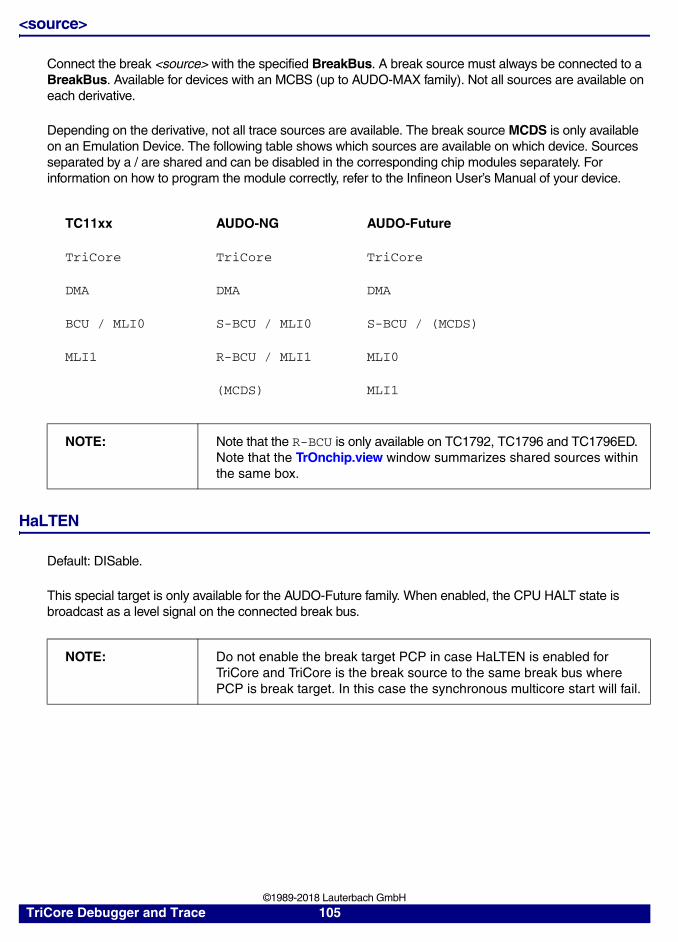
<source>
Connect the break <source> with the specified BreakBus. A break source must always be connected to a BreakBus. Available for devices with an MCBS (up to AUDO-MAX family). Not all sources are available on each derivative.
Depending on the derivative, not all trace sources are available. The break source MCDS is only available on an Emulation Device. The following table shows which sources are available on which device. Sources separated by a / are shared and can be disabled in the corresponding chip modules separately. For information on how to program the module correctly, refer to the Infineon User’s Manual of your device.
HaLTEN
Default: DISable.
This special target is only available for the AUDO-Future family. When enabled, the CPU HALT state is broadcast as a level signal on the connected break bus.
TC11xx AUDO-NG AUDO-Future
TriCore TriCore TriCore
DMA DMA DMA
BCU / MLI0 S-BCU / MLI0 S-BCU / (MCDS)
MLI1 R-BCU / MLI1 MLI0
(MCDS) MLI1
NOTE: Note that the R-BCU is only available on TC1792, TC1796 and TC1796ED.Note that the TrOnchip.view window summarizes shared sources within the same box.
NOTE: Do not enable the break target PCP in case HaLTEN is enabled for TriCore and TriCore is the break source to the same break bus where PCP is break target. In this case the synchronous multicore start will fail.
TriCore Debugger and Trace 105 ©1989-2018 Lauterbach GmbH
TrOnchip.CONVert Adjust range breakpoint in on-chip resource
Converts on-chip breakpoints, freeing on-chip breakpoint resources.
TrOnchip.CountX Event X counter value
This feature is only available for the 5 V trace preprocessor (LA-7879).
The counter <value> is incremented each time the event X has occurred. When the value is equal to 0, the assigned status (TR[1..0] CR or EXT) is sampled.
On 3.3 V preprocessors (LA-7928), this counter is not active, the status will be sampled every time the event X occurred.
TrOnchip.CountY Event Y counter value
See TrOnchip.CountX.
Format: TrOnchip.CONVert [ON | OFF]
ON On cores up to core version 1.3.1, breakpoint ranges will be reduced to single address breakpoints.
As of core version 1.6, breakpoint ranges from and to the same address will be converted to a single address breakpoint.
OFF No conversion.
Format: TrOnchip.CountX <value>
Format: TrOnchip.CountY <value>
TriCore Debugger and Trace 106 ©1989-2018 Lauterbach GmbH
TrOnchip.EXTernal Configure TriCore break on BreakBus event
Default: OFF.
When enabled, TriCore will break on an break signal distributed via the BreakBus which TriCore listens to.
For AURIX devices, this option is always on.
TrOnchip.RESet Reset settings for the on-chip trigger unit
Resets the settings for the trigger on-chip unit to default.
TrOnchip.SoftWare Configure "TriCore" break on debug instruction
Default: ON.
When enabled, TriCore will break when executing a debug instruction.
Format: TrOnchip.EXTernal [ON | OFF]
NOTE: Enabling this feature will disturb the OCDS-L2 break actions TraceON, TraceOFF, TraceEnable and TraceTrigger. Instead TriCore will stop when hitting such a break action.Unconditional tracing is still possible, OCDS-L3 (On-chip trace) is not affected.
Format: TrOnchip.RESet
Format: TrOnchip.SoftWare [ON | OFF]
NOTE: When this feature is disabled, the TriCore CPU will treat all debug instructions as nop instructions. This will silently disable all software breakpoints.
TriCore Debugger and Trace 107 ©1989-2018 Lauterbach GmbH
TrOnchip.SusSWitch Enable or disable suspend switch
Default: DISable.
Enable or disable forwarding of a break signal to the suspend bus.
Available for devices with an MCBS (up to AUDO-MAX family).
TrOnchip.SusSWitch.FORCE Force generation of suspend signal
Default: DISable.
When enabled, the suspend switch generates a suspend signal independent of any state or mode.
Available for devices with an MCBS (up to AUDO-MAX family).
TrOnchip.SusSWitch.Mode Set suspend switch mode
Default: CAPTURE.
In DIRECT mode, the suspend switch forwards the signal coming from the break bus directly to the suspend bus.
In CAPTURE mode, a high-low transition on the break bus is stored in a flip-flop. Its state is used to drive the suspend bus. The flip-flop is reset with the CLEAR option. Available for devices with an MCBS (up to AUDO-MAX family).
Format: TrOnchip.SusSwitch [ENable | DISable]
Format: TrOnchip.SusSwitch.FORCE [ENable | DISable]
Format: TrOnchip.SusSwitch.Mode [CAPTURE | DIRECT | CLEAR]
TriCore Debugger and Trace 108 ©1989-2018 Lauterbach GmbH
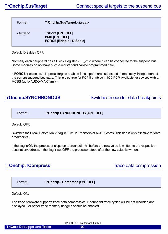
TrOnchip.SusTarget Connect special targets to the suspend bus
Default: DISable / OFF.
Normally each peripheral has a Clock Register mod_CLC where it can be connected to the suspend bus. Some modules do not have such a register and can be programmed here.
If FORCE is selected, all special targets enabled for suspend are suspended immediately, independent of the current suspend bus state. This is also true for PCP if enabled in ICD PCP. Available for devices with an MCBS (up to AUDO-MAX family).
TrOnchip.SYNCHRONOUS Switches mode for data breakpoints
Default: OFF.
Switches the Break Before Make flag in TRxEVT registers of AURIX cores. This flag is only effective for data breakpoints.
If the flag is ON the processor stops on a breakpoint hit before the new value is written to the respective destination/address. If the flag is set OFF the processor stops after the new value is written.
TrOnchip.TCompress Trace data compression
Default: ON.
The trace hardware supports trace data compression. Redundant trace cycles will be not recorded and displayed. For better trace memory usage it should be enabled.
Format: TrOnchip.SusTarget.<target>
<target>: TriCore [ON | OFF]PMU [ON | OFF]FORCE [ENable | DISable]
Format: TrOnchip.SYNCHRONOUS [ON | OFF]
Format: TrOnchip.TCompress [ON | OFF]
TriCore Debugger and Trace 109 ©1989-2018 Lauterbach GmbH
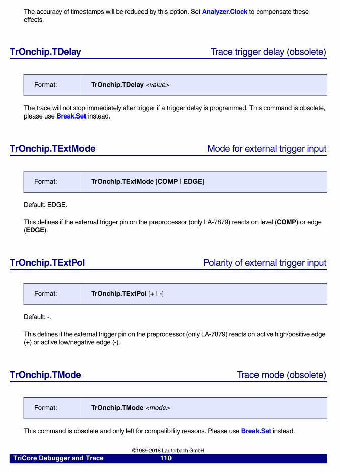
The accuracy of timestamps will be reduced by this option. Set Analyzer.Clock to compensate these effects.
TrOnchip.TDelay Trace trigger delay (obsolete)
The trace will not stop immediately after trigger if a trigger delay is programmed. This command is obsolete, please use Break.Set instead.
TrOnchip.TExtMode Mode for external trigger input
Default: EDGE.
This defines if the external trigger pin on the preprocessor (only LA-7879) reacts on level (COMP) or edge (EDGE).
TrOnchip.TExtPol Polarity of external trigger input
Default: -.
This defines if the external trigger pin on the preprocessor (only LA-7879) reacts on active high/positive edge (+) or active low/negative edge (-).
TrOnchip.TMode Trace mode (obsolete)
This command is obsolete and only left for compatibility reasons. Please use Break.Set instead.
Format: TrOnchip.TDelay <value>
Format: TrOnchip.TExtMode [COMP | EDGE]
Format: TrOnchip.TExtPol [+ | -]
Format: TrOnchip.TMode <mode>
TriCore Debugger and Trace 110 ©1989-2018 Lauterbach GmbH
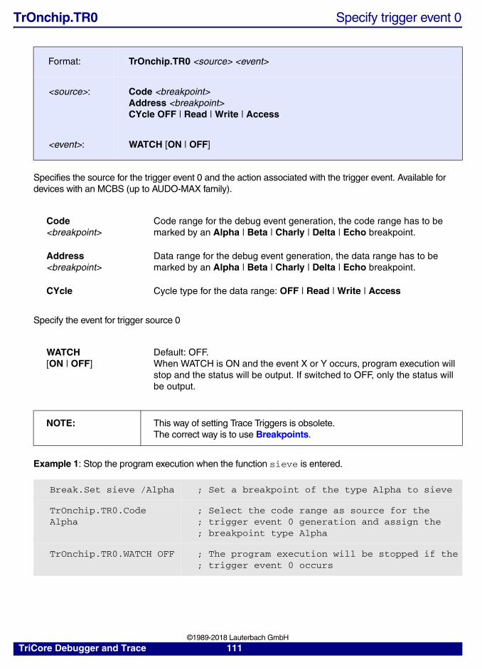
TrOnchip.TR0 Specify trigger event 0
Specifies the source for the trigger event 0 and the action associated with the trigger event. Available for devices with an MCBS (up to AUDO-MAX family).
Specify the event for trigger source 0
Example 1: Stop the program execution when the function sieve is entered.
Format: TrOnchip.TR0 <source> <event>
<source>: Code <breakpoint>Address <breakpoint>CYcle OFF | Read | Write | Access
<event>: WATCH [ON | OFF]
Code<breakpoint>
Code range for the debug event generation, the code range has to be marked by an Alpha | Beta | Charly | Delta | Echo breakpoint.
Address <breakpoint>
Data range for the debug event generation, the data range has to be marked by an Alpha | Beta | Charly | Delta | Echo breakpoint.
CYcle Cycle type for the data range: OFF | Read | Write | Access
WATCH[ON | OFF]
Default: OFF. When WATCH is ON and the event X or Y occurs, program execution will stop and the status will be output. If switched to OFF, only the status will be output.
NOTE: This way of setting Trace Triggers is obsolete. The correct way is to use Breakpoints.
Break.Set sieve /Alpha ; Set a breakpoint of the type Alpha to sieve
TrOnchip.TR0.Code Alpha
; Select the code range as source for the; trigger event 0 generation and assign the; breakpoint type Alpha
TrOnchip.TR0.WATCH OFF ; The program execution will be stopped if the; trigger event 0 occurs
TriCore Debugger and Trace 111 ©1989-2018 Lauterbach GmbH
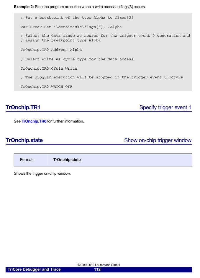
Example 2: Stop the program execution when a write access to flags[3] occurs.
TrOnchip.TR1 Specify trigger event 1
See TrOnchip.TR0 for further information.
TrOnchip.state Show on-chip trigger window
Shows the trigger on-chip window.
; Set a breakpoint of the type Alpha to flags[3]
Var.Break.Set \\demo\taskc\flags[3]; /Alpha
; Select the data range as source for the trigger event 0 generation and; assign the breakpoint type Alpha
TrOnchip.TR0.Address Alpha
; Select Write as cycle type for the data access
TrOnchip.TR0.CYcle Write
; The program execution will be stopped if the trigger event 0 occurs
TrOnchip.TR0.WATCH OFF
Format: TrOnchip.state
TriCore Debugger and Trace 112 ©1989-2018 Lauterbach GmbH

TrOnchip.X Select trigger source X
The on-chip comparator unit can react on different sources. Available for devices with an MCBS (up to AUDO-MAX family).
TrOnchip.Y Select trigger source Y
See TrOnchip.X for further information.
Format: TrOnchip.X <source>
<source>: TR0TR1CREXT
TR0 On-chip address comparator TR0
TR1 On-chip address comparator TR1
CR Core Event: MTCR/ MFCR instruction is executed or a core SFR is modified.
EXT External Break In pin is asserted.
TriCore Debugger and Trace 113 ©1989-2018 Lauterbach GmbH
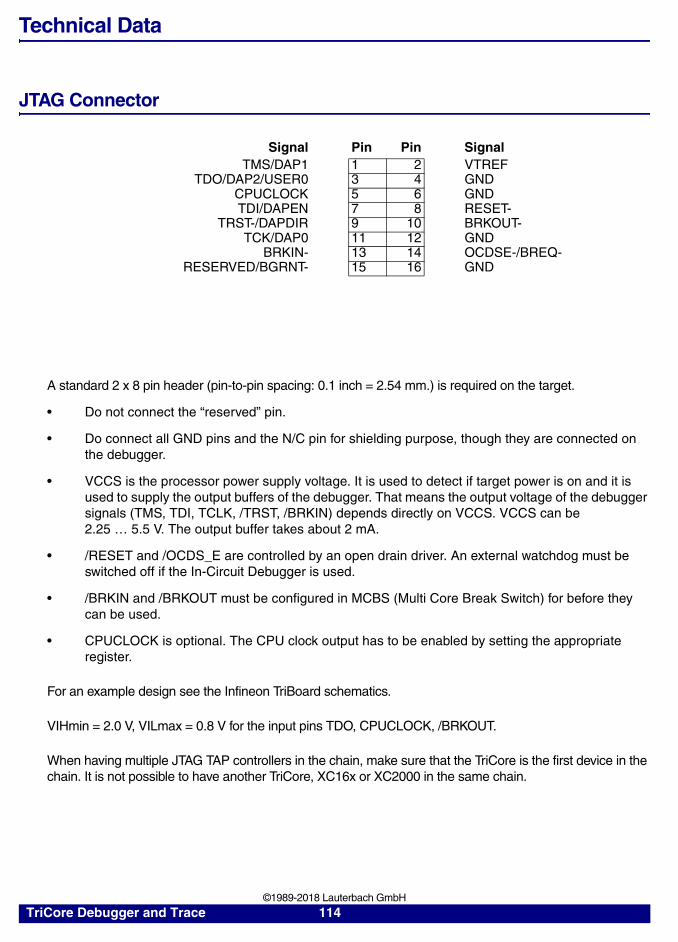
Technical Data
JTAG Connector
A standard 2 x 8 pin header (pin-to-pin spacing: 0.1 inch = 2.54 mm.) is required on the target.
• Do not connect the “reserved” pin.
• Do connect all GND pins and the N/C pin for shielding purpose, though they are connected on the debugger.
• VCCS is the processor power supply voltage. It is used to detect if target power is on and it is used to supply the output buffers of the debugger. That means the output voltage of the debugger signals (TMS, TDI, TCLK, /TRST, /BRKIN) depends directly on VCCS. VCCS can be 2.25 … 5.5 V. The output buffer takes about 2 mA.
• /RESET and /OCDS_E are controlled by an open drain driver. An external watchdog must be switched off if the In-Circuit Debugger is used.
• /BRKIN and /BRKOUT must be configured in MCBS (Multi Core Break Switch) for before they can be used.
• CPUCLOCK is optional. The CPU clock output has to be enabled by setting the appropriate register.
For an example design see the Infineon TriBoard schematics.
VIHmin = 2.0 V, VILmax = 0.8 V for the input pins TDO, CPUCLOCK, /BRKOUT.
When having multiple JTAG TAP controllers in the chain, make sure that the TriCore is the first device in the chain. It is not possible to have another TriCore, XC16x or XC2000 in the same chain.
Signal Pin Pin SignalTMS/DAP1 1 2 VTREF
TDO/DAP2/USER0 3 4 GNDCPUCLOCK 5 6 GNDTDI/DAPEN 7 8 RESET-
TRST-/DAPDIR 9 10 BRKOUT-TCK/DAP0 11 12 GND
BRKIN- 13 14 OCDSE-/BREQ-RESERVED/BGRNT- 15 16 GND
TriCore Debugger and Trace 114 ©1989-2018 Lauterbach GmbH
See ”Application Note Debug Cable TriCore” (tricore_app_ocds.pdf) for a description of
• The TriCore Debug Cables and their features
• The JTAG and DAP connectors
• Availably accessories: adapters, converters and cables
Pins Connection Description Recommendations
1 TMS Test Mode Select
None.
2 VCCS VCC Sense Connect to Chip I/O voltage VCC.
3 TDO Test Data Out If there are multiple devices on the JTAG chain, connect TDO to the TDI signal of the next device in the chain.
4, 6, 12 GND System Ground Plan
Connect to digital ground.
5 CPUCLOCK CPU clock Optional.
7 TDI Test Data In No other devices in the JTAG chain are allowed between the Debug Cable and the TriCore.
8 RESET Reset Connect to /PORST and connect /PORST to VCC via a 10 k pull-up resistor.Do not connect to /TRST.
9 TRST Test Reset Connect to /TRST. Do not connect to /PORST.
10 BRKOUT Break output None.
11 TCLK Test clock None.
13 BRKIN Break input None.
14 OCDSE OCDS enable Required for older TriCore devices only, e.g. TC1765, TC1775 and TC19xx. Connect to VCC via a 10 k pull-up resistor.
15 NC Not Connected
Connect to Ground.
16 GND KEY pin. Connect to Ground.
TriCore Debugger and Trace 115 ©1989-2018 Lauterbach GmbH
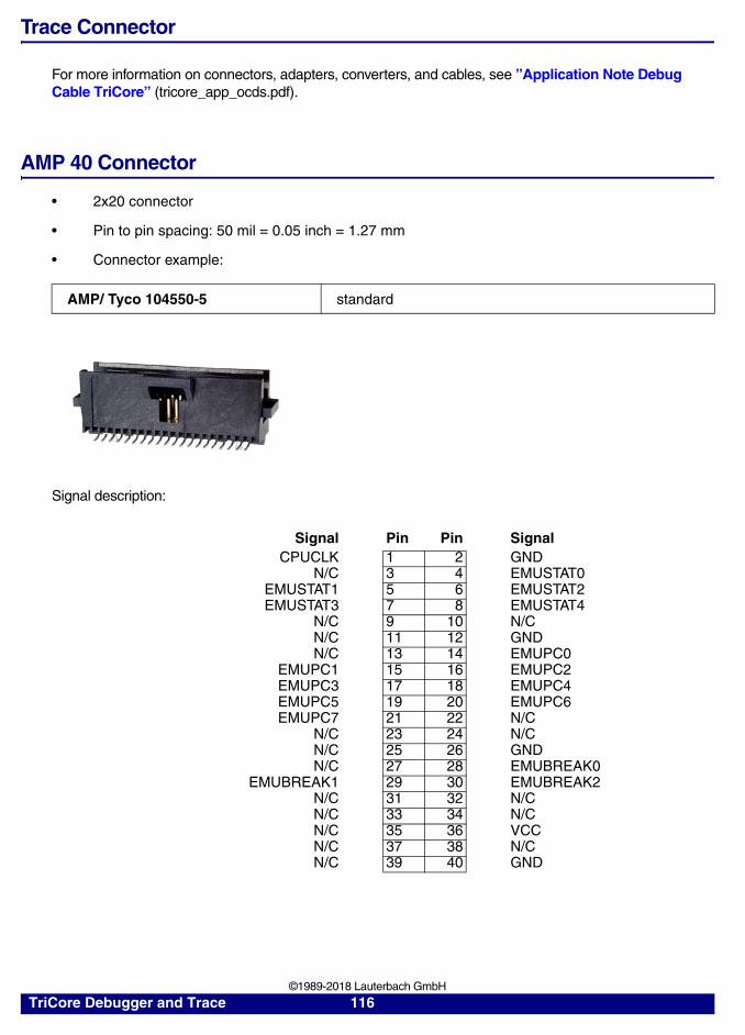
Trace Connector
For more information on connectors, adapters, converters, and cables, see ”Application Note Debug Cable TriCore” (tricore_app_ocds.pdf).
AMP 40 Connector
• 2x20 connector
• Pin to pin spacing: 50 mil = 0.05 inch = 1.27 mm
• Connector example:
Signal description:
AMP/ Tyco 104550-5 standard
Signal Pin Pin SignalCPUCLK 1 2 GND
N/C 3 4 EMUSTAT0EMUSTAT1 5 6 EMUSTAT2EMUSTAT3 7 8 EMUSTAT4
N/C 9 10 N/CN/C 11 12 GNDN/C 13 14 EMUPC0
EMUPC1 15 16 EMUPC2EMUPC3 17 18 EMUPC4EMUPC5 19 20 EMUPC6EMUPC7 21 22 N/C
N/C 23 24 N/CN/C 25 26 GNDN/C 27 28 EMUBREAK0
EMUBREAK1 29 30 EMUBREAK2N/C 31 32 N/CN/C 33 34 N/CN/C 35 36 VCCN/C 37 38 N/CN/C 39 40 GND
TriCore Debugger and Trace 116 ©1989-2018 Lauterbach GmbH
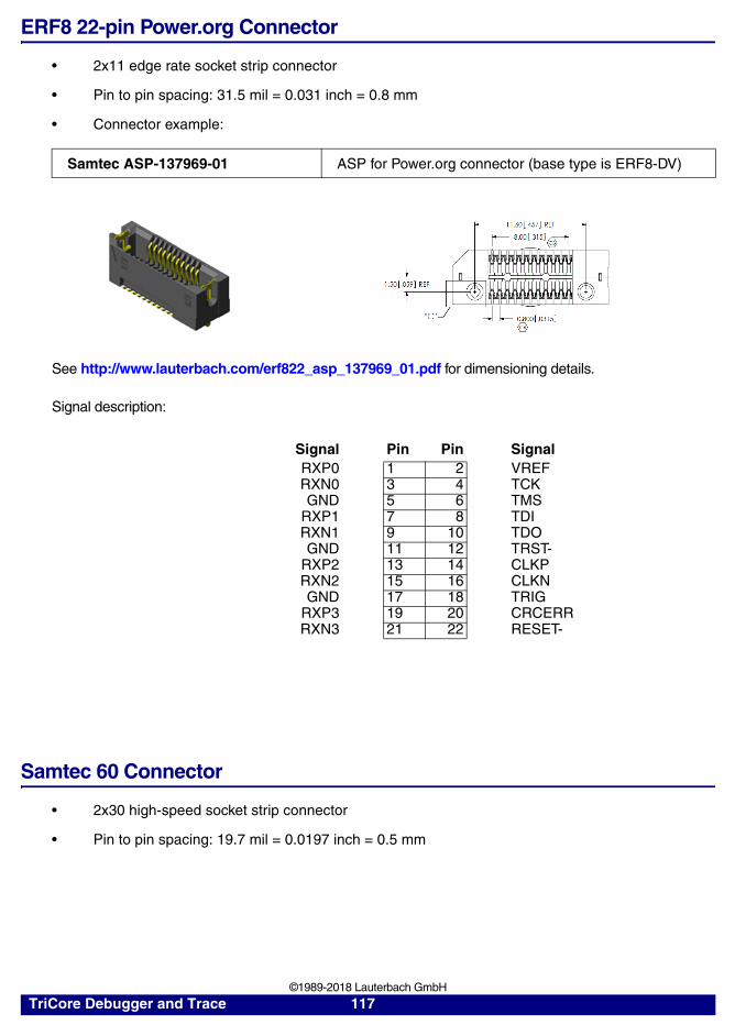
ERF8 22-pin Power.org Connector
• 2x11 edge rate socket strip connector
• Pin to pin spacing: 31.5 mil = 0.031 inch = 0.8 mm
• Connector example:
See http://www.lauterbach.com/erf822_asp_137969_01.pdf for dimensioning details.
Signal description:
Samtec 60 Connector
• 2x30 high-speed socket strip connector
• Pin to pin spacing: 19.7 mil = 0.0197 inch = 0.5 mm
Samtec ASP-137969-01 ASP for Power.org connector (base type is ERF8-DV)
Signal Pin Pin SignalRXP0 1 2 VREFRXN0 3 4 TCKGND 5 6 TMS
RXP1 7 8 TDIRXN1 9 10 TDOGND 11 12 TRST-
RXP2 13 14 CLKPRXN2 15 16 CLKNGND 17 18 TRIG
RXP3 19 20 CRCERRRXN3 21 22 RESET-
TriCore Debugger and Trace 117 ©1989-2018 Lauterbach GmbH
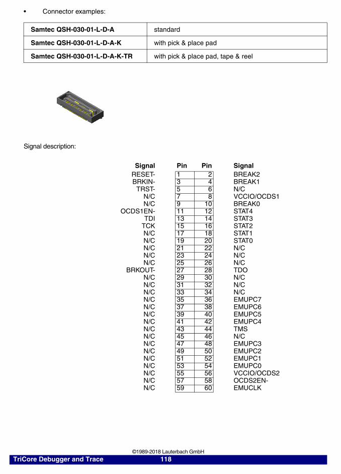
• Connector examples:
Signal description:
Samtec QSH-030-01-L-D-A standard
Samtec QSH-030-01-L-D-A-K with pick & place pad
Samtec QSH-030-01-L-D-A-K-TR with pick & place pad, tape & reel
Signal Pin Pin SignalRESET- 1 2 BREAK2BRKIN- 3 4 BREAK1
TRST- 5 6 N/CN/C 7 8 VCCIO/OCDS1N/C 9 10 BREAK0
OCDS1EN- 11 12 STAT4TDI 13 14 STAT3
TCK 15 16 STAT2N/C 17 18 STAT1N/C 19 20 STAT0N/C 21 22 N/CN/C 23 24 N/CN/C 25 26 N/C
BRKOUT- 27 28 TDON/C 29 30 N/CN/C 31 32 N/CN/C 33 34 N/CN/C 35 36 EMUPC7N/C 37 38 EMUPC6N/C 39 40 EMUPC5N/C 41 42 EMUPC4N/C 43 44 TMSN/C 45 46 N/CN/C 47 48 EMUPC3N/C 49 50 EMUPC2N/C 51 52 EMUPC1N/C 53 54 EMUPC0N/C 55 56 VCCIO/OCDS2N/C 57 58 OCDS2EN-N/C 59 60 EMUCLK
TriCore Debugger and Trace 118 ©1989-2018 Lauterbach GmbH
Technical Data for Debugger
Operation Voltage
Mechanical Dimensions
The Debug Cables with new housings are shipped within Europe since March 2006. They have a removable cable and are RoHS compliant. The electrical components and the schematics are identical to ones in the old housing.
Further details are available in “Application Note Debug Cable TriCore” (tricore_app_ocds.pdf).
Adapter OrderNo Voltage Range
Debugger for TriCore Automotive LA-3737 1.6 .. 5.5 VDebugger-Bundle MPC5xxx/TriCore Automotive LA-3738 1.6 .. 5.5 VDebugger for TriCore Standard Additional LA-7756A 2.5 .. 5.2 V
OCDS Uni-Dir Debug Cable V0
Bidirectional Cables and Auto-motive Debug Cables
Length: 4.2 cm 5.5 cm
Width: 5.2 cm 6.25 cm
Height: 1.6 cm 1.7 cm
Length of cable: approx. 37.5 cm approx. 37.8 cm
TriCore Debugger and Trace 119 ©1989-2018 Lauterbach GmbH

Technical Data for Trace
Operation Frequency
Operation Voltage
Module CPU TRACE
LA-7928 PXB4260 130.0 MHzLA-7928 TC10GP 180.0 MHzLA-7928 TC1100 180.0 MHzLA-7928 TC1115 180.0 MHzLA-7928 TC1130 180.0 MHzLA-7928 TC1161 180.0 MHzLA-7928 TC1162 180.0 MHzLA-7928 TC1163 180.0 MHzLA-7928 TC1164 180.0 MHzLA-7928 TC1165 180.0 MHzLA-7928 TC1166 180.0 MHzLA-7928 TC11IA 180.0 MHzLA-7928 TC11IB 180.0 MHzLA-7928 TC11IC 180.0 MHzLA-7928 TC1762LA-7928 TC1764LA-7928 TC1765 180.0 MHzLA-7928 TC1766LA-7928 TC1766ED 180.0 MHzLA-7928 TC1775 180.0 MHzLA-7928 TC1792 180.0 MHzLA-7928 TC1796 180.0 MHzLA-7928 TC1796ED 180.0 MHzLA-7928 TC1796L 180.0 MHzLA-7928 TC1910 180.0 MHzLA-7928 TC1912 180.0 MHzLA-7928 TC1920 180.0 MHz
Adapter OrderNo Voltage Range
Preprocessor TriCore OCDS-L2 5V Samtec 60 LA-7879 3.0 .. 5.5 VConverter AMP 40 to Samtec 60 LA-7919 3.0 .. 5.5 VPreprocessor TriCore OCDS-L2 3.3V Samtec 60 LA-7928 1.8 .. 3.3 V
TriCore Debugger and Trace 120 ©1989-2018 Lauterbach GmbH
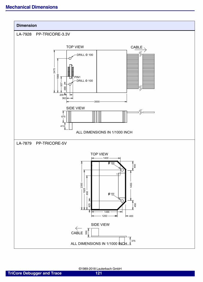
Mechanical Dimensions
Dimension
LA-7928 PP-TRICORE-3.3V
LA-7879 PP-TRICORE-5V
PIN1
DRILL O 100/
3500
362200
488
93
7
198
8
24
75
675
413
TOP VIEW
SIDE VIEW
CABLE
ALL DIMENSIONS IN 1/1000 INCH
DRILL O 100/
TOP VIEW
SIDE VIEW
CABLE
ALL DIMENSIONS IN 1/1000 INCH
550
375
4001250
1488
450
145
0
45
0
1
100
1400
100
235
01
925
650
425
TriCore Debugger and Trace 121 ©1989-2018 Lauterbach GmbH
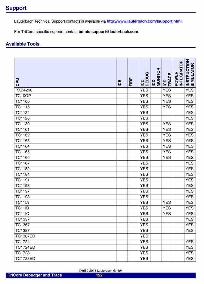
Support
Lauterbach Technical Support contacts is available via http://www.lauterbach.com/tsupport.html.
For TriCore specific support contact [email protected].
Available Tools
CP
U
ICE
FIR
E
ICD
DE
BU
G
ICD
MO
NIT
OR
ICD
TR
AC
E
PO
WE
RIN
TE
GR
ATO
R
INS
TR
UC
TIO
NS
IMU
LA
TOR
PXB4260 YES YES YESTC10GP YES YES YESTC1100 YES YES YESTC1115 YES YES YESTC1124 YES YESTC1128 YES YESTC1130 YES YES YESTC1161 YES YES YESTC1162 YES YES YESTC1163 YES YES YESTC1164 YES YES YESTC1165 YES YES YESTC1166 YES YES YESTC1167 YES YESTC1182 YES YESTC1184 YES YESTC1191 YES YESTC1193 YES YESTC1197 YES YESTC1198 YES YESTC11IA YES YES YESTC11IB YES YES YESTC11IC YES YES YESTC1337 YES YESTC1367 YES YESTC1387 YES YESTC1387ED YESTC1724 YES YESTC1724ED YES YESTC1728 YES YESTC1728ED YES YES
TriCore Debugger and Trace 122 ©1989-2018 Lauterbach GmbH
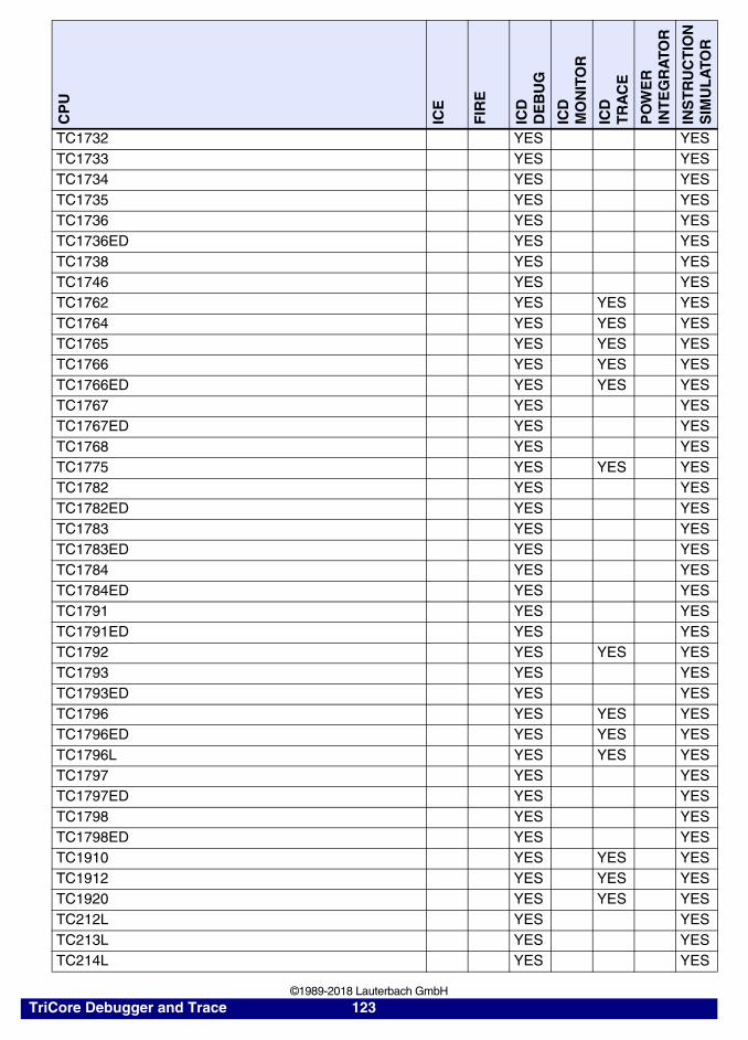
TC1732 YES YESTC1733 YES YESTC1734 YES YESTC1735 YES YESTC1736 YES YESTC1736ED YES YESTC1738 YES YESTC1746 YES YESTC1762 YES YES YESTC1764 YES YES YESTC1765 YES YES YESTC1766 YES YES YESTC1766ED YES YES YESTC1767 YES YESTC1767ED YES YESTC1768 YES YESTC1775 YES YES YESTC1782 YES YESTC1782ED YES YESTC1783 YES YESTC1783ED YES YESTC1784 YES YESTC1784ED YES YESTC1791 YES YESTC1791ED YES YESTC1792 YES YES YESTC1793 YES YESTC1793ED YES YESTC1796 YES YES YESTC1796ED YES YES YESTC1796L YES YES YESTC1797 YES YESTC1797ED YES YESTC1798 YES YESTC1798ED YES YESTC1910 YES YES YESTC1912 YES YES YESTC1920 YES YES YESTC212L YES YESTC213L YES YESTC214L YES YES
CP
U
ICE
FIR
E
ICD
DE
BU
G
ICD
MO
NIT
OR
ICD
TR
AC
E
PO
WE
RIN
TE
GR
ATO
R
INS
TR
UC
TIO
NS
IMU
LA
TOR
TriCore Debugger and Trace 123 ©1989-2018 Lauterbach GmbH
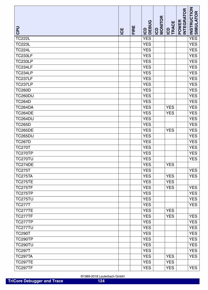
TC222L YES YESTC223L YES YESTC224L YES YESTC233LF YES YESTC233LP YES YESTC234LF YES YESTC234LP YES YESTC237LF YES YESTC237LP YES YESTC260D YES YESTC260DU YES YESTC264D YES YESTC264DA YES YES YESTC264DE YES YES YESTC264DU YES YESTC265D YES YESTC265DE YES YES YESTC265DU YES YESTC267D YES YESTC270T YES YESTC270TP YES YESTC270TU YES YESTC274DE YES YESTC275T YES YESTC275TA YES YES YESTC275TE YES YESTC275TF YES YES YESTC275TP YES YESTC275TU YES YESTC277T YES YESTC277TE YES YESTC277TF YES YES YESTC277TP YES YESTC277TU YES YESTC290T YES YESTC290TP YES YESTC290TU YES YESTC297T YES YESTC297TA YES YES YESTC297TE YES YESTC297TF YES YES YES
CP
U
ICE
FIR
E
ICD
DE
BU
G
ICD
MO
NIT
OR
ICD
TR
AC
E
PO
WE
RIN
TE
GR
ATO
R
INS
TR
UC
TIO
NS
IMU
LA
TOR
TriCore Debugger and Trace 124 ©1989-2018 Lauterbach GmbH
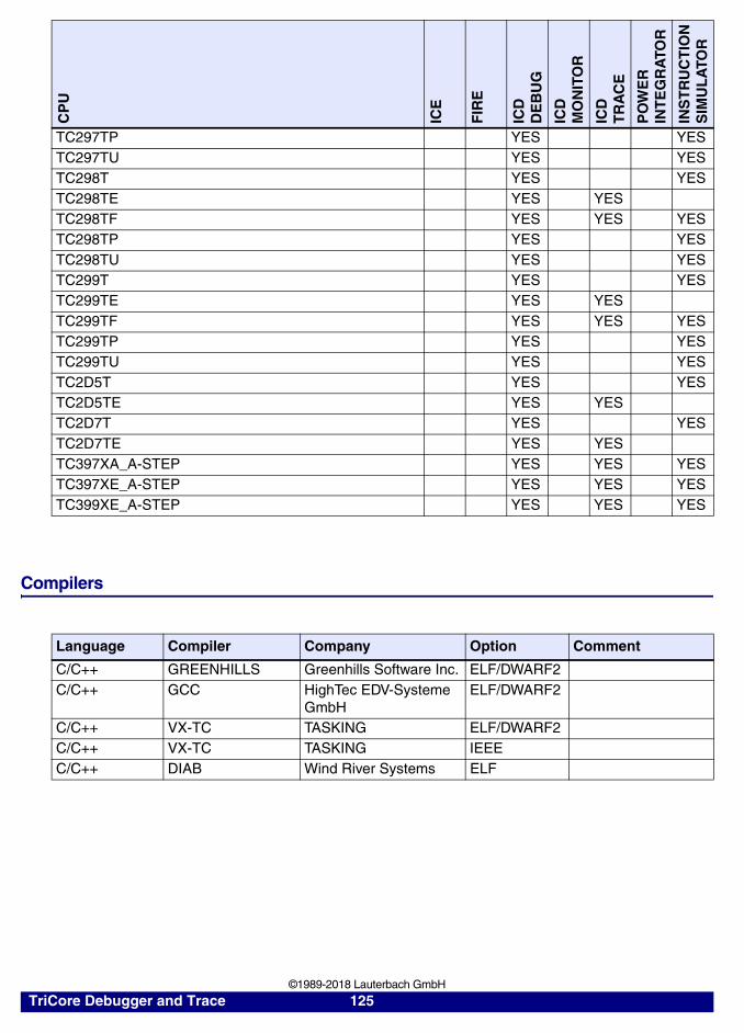
Compilers
TC297TP YES YESTC297TU YES YESTC298T YES YESTC298TE YES YESTC298TF YES YES YESTC298TP YES YESTC298TU YES YESTC299T YES YESTC299TE YES YESTC299TF YES YES YESTC299TP YES YESTC299TU YES YESTC2D5T YES YESTC2D5TE YES YESTC2D7T YES YESTC2D7TE YES YESTC397XA_A-STEP YES YES YESTC397XE_A-STEP YES YES YESTC399XE_A-STEP YES YES YES
Language Compiler Company Option Comment
C/C++ GREENHILLS Greenhills Software Inc. ELF/DWARF2C/C++ GCC HighTec EDV-Systeme
GmbHELF/DWARF2
C/C++ VX-TC TASKING ELF/DWARF2C/C++ VX-TC TASKING IEEEC/C++ DIAB Wind River Systems ELF
CP
U
ICE
FIR
E
ICD
DE
BU
G
ICD
MO
NIT
OR
ICD
TR
AC
E
PO
WE
RIN
TE
GR
ATO
R
INS
TR
UC
TIO
NS
IMU
LA
TOR
TriCore Debugger and Trace 125 ©1989-2018 Lauterbach GmbH
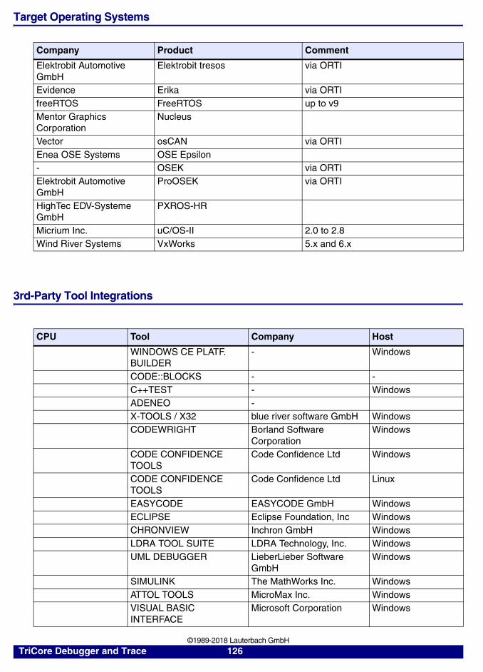
Target Operating Systems
3rd-Party Tool Integrations
Company Product Comment
Elektrobit Automotive GmbH
Elektrobit tresos via ORTI
Evidence Erika via ORTIfreeRTOS FreeRTOS up to v9Mentor Graphics Corporation
Nucleus
Vector osCAN via ORTIEnea OSE Systems OSE Epsilon- OSEK via ORTIElektrobit Automotive GmbH
ProOSEK via ORTI
HighTec EDV-Systeme GmbH
PXROS-HR
Micrium Inc. uC/OS-II 2.0 to 2.8Wind River Systems VxWorks 5.x and 6.x
CPU Tool Company Host
WINDOWS CE PLATF. BUILDER
- Windows
CODE::BLOCKS - -C++TEST - WindowsADENEO -X-TOOLS / X32 blue river software GmbH WindowsCODEWRIGHT Borland Software
CorporationWindows
CODE CONFIDENCE TOOLS
Code Confidence Ltd Windows
CODE CONFIDENCE TOOLS
Code Confidence Ltd Linux
EASYCODE EASYCODE GmbH WindowsECLIPSE Eclipse Foundation, Inc WindowsCHRONVIEW Inchron GmbH WindowsLDRA TOOL SUITE LDRA Technology, Inc. WindowsUML DEBUGGER LieberLieber Software
GmbHWindows
SIMULINK The MathWorks Inc. WindowsATTOL TOOLS MicroMax Inc. WindowsVISUAL BASIC INTERFACE
Microsoft Corporation Windows
TriCore Debugger and Trace 126 ©1989-2018 Lauterbach GmbH
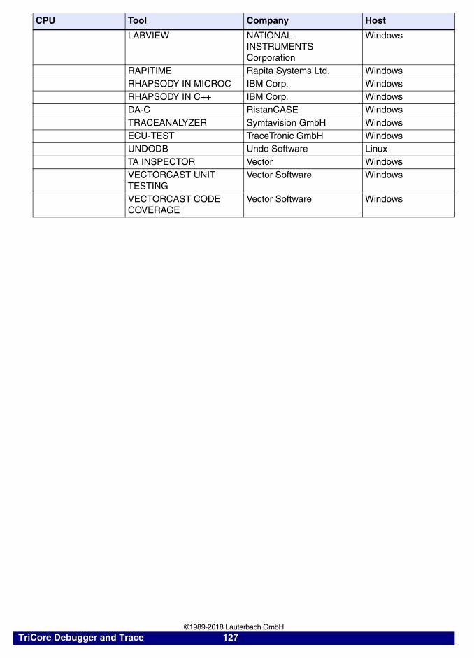
LABVIEW NATIONAL INSTRUMENTS Corporation
Windows
RAPITIME Rapita Systems Ltd. WindowsRHAPSODY IN MICROC IBM Corp. WindowsRHAPSODY IN C++ IBM Corp. WindowsDA-C RistanCASE WindowsTRACEANALYZER Symtavision GmbH WindowsECU-TEST TraceTronic GmbH WindowsUNDODB Undo Software LinuxTA INSPECTOR Vector WindowsVECTORCAST UNIT TESTING
Vector Software Windows
VECTORCAST CODE COVERAGE
Vector Software Windows
CPU Tool Company Host
TriCore Debugger and Trace 127 ©1989-2018 Lauterbach GmbH
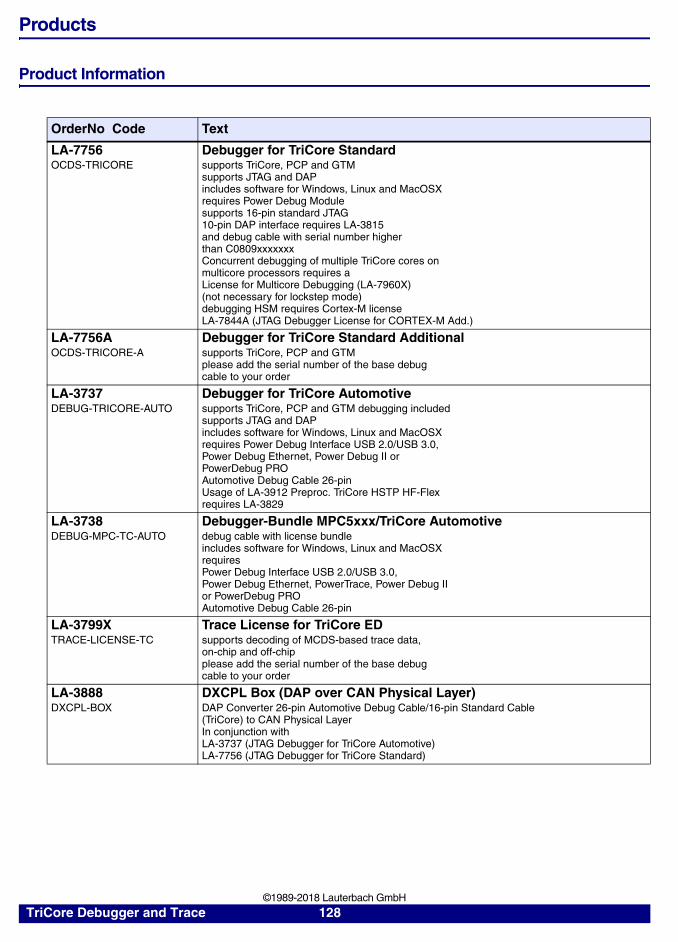
Products
Product Information
OrderNo Code Text
LA-7756 OCDS-TRICORE
Debugger for TriCore Standardsupports TriCore, PCP and GTMsupports JTAG and DAPincludes software for Windows, Linux and MacOSXrequires Power Debug Modulesupports 16-pin standard JTAG10-pin DAP interface requires LA-3815and debug cable with serial number higherthan C0809xxxxxxxConcurrent debugging of multiple TriCore cores onmulticore processors requires aLicense for Multicore Debugging (LA-7960X)(not necessary for lockstep mode)debugging HSM requires Cortex-M licenseLA-7844A (JTAG Debugger License for CORTEX-M Add.)
LA-7756A OCDS-TRICORE-A
Debugger for TriCore Standard Additionalsupports TriCore, PCP and GTMplease add the serial number of the base debugcable to your order
LA-3737 DEBUG-TRICORE-AUTO
Debugger for TriCore Automotivesupports TriCore, PCP and GTM debugging includedsupports JTAG and DAPincludes software for Windows, Linux and MacOSXrequires Power Debug Interface USB 2.0/USB 3.0,Power Debug Ethernet, Power Debug II orPowerDebug PROAutomotive Debug Cable 26-pinUsage of LA-3912 Preproc. TriCore HSTP HF-Flexrequires LA-3829
LA-3738 DEBUG-MPC-TC-AUTO
Debugger-Bundle MPC5xxx/TriCore Automotivedebug cable with license bundleincludes software for Windows, Linux and MacOSXrequiresPower Debug Interface USB 2.0/USB 3.0,Power Debug Ethernet, PowerTrace, Power Debug IIor PowerDebug PROAutomotive Debug Cable 26-pin
LA-3799X TRACE-LICENSE-TC
Trace License for TriCore EDsupports decoding of MCDS-based trace data,on-chip and off-chipplease add the serial number of the base debugcable to your order
LA-3888 DXCPL-BOX
DXCPL Box (DAP over CAN Physical Layer)DAP Converter 26-pin Automotive Debug Cable/16-pin Standard Cable(TriCore) to CAN Physical LayerIn conjunction withLA-3737 (JTAG Debugger for TriCore Automotive)LA-7756 (JTAG Debugger for TriCore Standard)
TriCore Debugger and Trace 128 ©1989-2018 Lauterbach GmbH

LA-3843 CON-JTAG14/16-JTAG10
Conv. AUTO-26/OnCE14-PPC/JTAG16-TC to ECU14JTAG Converter 26-pin Automotive Debug Cable(PPC/ TriCore) to 10-pin JTAG half-size(Automotive, ECU14)forLA-3736 (JTAG Debugger for MPC5xxx Automotive)LA-3737 (JTAG Debugger for TriCore Automotive)andJTAG Converter 14-pin OnCE-PPC to10-pin JTAG half-size (Automotive, ECU14)for LA-7753 (JTAG Debugger for MPC55xx/MPC56xx)andJTAG Converter 16-pin TriCore to10-pin JTAG half-size (Automotive, ECU14)also supporting DAP (2-wire)for LA-7756 (OCDS Debugger for TriCore)
LA-3848 CON-JTAG16-AUTO26
Conv. JTAG16-TriCore to AUTO-26Converter 16-pin JTAG (TriCore)to 26-pin Automotive Debug Cablealso supporting DAP (2-wire)for LA-7756 (OCDS Debugger for TriCore)
LA-3849 CON-AUTO26-JTAG16
Conv. AUTO26 to JTAG16-TriCoreConverter 26-pin Automotive Debug Cableto 16-pin JTAG (TriCore)also supporting DAP (2-wire)forLA-3737 (JTAG Debugger for TriCore Automotive)
LA-7941 CON-JTAG16-SAM-TC
Conv. 16 Pin OCDS-L1 to Samtec 60 for TriCoreConverter 16 Pin OCDS level 1 connector toSamtec 60 Tricore trace connector on target
LA-3819 CON-JTAG16-MEDC17
Conv. 16 Pin JTAG to 10 Pin BOSCH MEDC17Converter 16 Pin JTAG to 10 PinHalf-Size-Connector for BOSCH MEDC17requires LA-7756 (OCDS Debugger for TriCore)
OrderNo Code Text
LA-7928 PP-TRICORE-3.3V
Preprocessor TriCore OCDS-L2 3.3V Samtec 60Program flow trace for TriCore OCDS Level2connector (Samtec60), cable and software180 MHz clock speed, 1.8 - 3.3 V4 x RISC-Trace-Depthconverter LA-7927 required for AMP40 connection
LA-7919 ICD-TC-CON-40/60
Converter AMP 40 to Samtec 60Converter for TriCore Level2from AMP 40 pin (preprocessor)to SAMTEC 60 pin (target)
LA-7927 ICD-TC-CON-60/40
Converter Samtec 60 to AMP 40Converter for TriCore Level2from SAMTEC 60 pin (preprocessor)to AMP 40 pin (target)
OrderNo Code Text
TriCore Debugger and Trace 129 ©1989-2018 Lauterbach GmbH
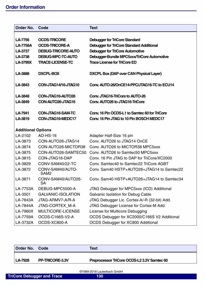
Order Information
Order No. Code Text
LA-7756 OCDS-TRICORE Debugger for TriCore StandardLA-7756A OCDS-TRICORE-A Debugger for TriCore Standard AdditionalLA-3737 DEBUG-TRICORE-AUTO Debugger for TriCore AutomotiveLA-3738 DEBUG-MPC-TC-AUTO Debugger-Bundle MPC5xxx/TriCore AutomotiveLA-3799X TRACE-LICENSE-TC Trace License for TriCore ED
LA-3888 DXCPL-BOX DXCPL Box (DAP over CAN Physical Layer)
LA-3843 CON-JTAG14/16-JTAG10 Conv. AUTO-26/OnCE14-PPC/JTAG16-TC to ECU14
LA-3848 CON-JTAG16-AUTO26 Conv. JTAG16-TriCore to AUTO-26LA-3849 CON-AUTO26-JTAG16 Conv. AUTO26 to JTAG16-TriCore
LA-7941 CON-JTAG16-SAM-TC Conv. 16 Pin OCDS-L1 to Samtec 60 for TriCoreLA-3819 CON-JTAG16-MEDC17 Conv. 16 Pin JTAG to 10 Pin BOSCH MEDC17
Additional OptionsLA-2102 AD-HS-16 Adapter Half-Size 16 pinLA-3873 CON-AUTO26-JTAG14 Conv. AUTO26 to JTAG14 OnCELA-3874 CON-AUTO26-MICTOR38 Conv. AUTO26 to MICTOR38 MPC5xxxLA-3875 CON-AUTO26-SAMTEC50 Conv. AUTO26 to Samtec50 MPC5xxxLA-3815 CON-JTAG16-DAP Conv. 16 Pin JTAG to DAP for TriCore/XC2000LA-3829 CONV-SAM40/22-TC Conv. Samtec40 to Samtec22 TriCore AGBTLA-3872 CONV-SAM40/AUTO-
SAM2Conv. Sam40 HSTP+AUTO26+JTAG14 to Samtec22
LA-3871 CONV-SAM40/AUTO26-SA
Conv. Sam40 HSTP+AUTO26+JTAG14 to Samtec34
LA-7753A DEBUG-MPC5500-A JTAG Debugger for MPC5xxx (ICD) AdditionalLA-3501 GALVANIC-ISOLATION Galvanic Isolation for Debug CableLA-7843A JTAG-ARMV7-A/R-A JTAG Debugger Lic. Cortex-A/-R (32-bit) Add.LA-7844A JTAG-CORTEX_M-A JTAG Debugger License for Cortex-M Add.LA-7960X MULTICORE-LICENSE License for Multicore DebuggingLA-7759A OCDS-C166S-V2-A OCDS Debugger for XC2000/C166S V2 AdditionalLA-3732A OCDS-XC800-A OCDS Debugger for XC800 Additional
Order No. Code Text
LA-7928 PP-TRICORE-3.3V Preprocessor TriCore OCDS-L2 3.3V Samtec 60
TriCore Debugger and Trace 130 ©1989-2018 Lauterbach GmbH
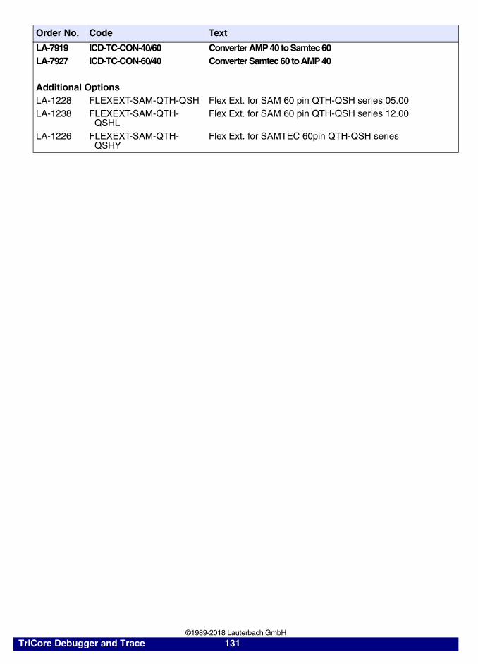
LA-7919 ICD-TC-CON-40/60 Converter AMP 40 to Samtec 60LA-7927 ICD-TC-CON-60/40 Converter Samtec 60 to AMP 40
Additional OptionsLA-1228 FLEXEXT-SAM-QTH-QSH Flex Ext. for SAM 60 pin QTH-QSH series 05.00LA-1238 FLEXEXT-SAM-QTH-
QSHLFlex Ext. for SAM 60 pin QTH-QSH series 12.00
LA-1226 FLEXEXT-SAM-QTH-QSHY
Flex Ext. for SAMTEC 60pin QTH-QSH series
Order No. Code Text
TriCore Debugger and Trace 131 ©1989-2018 Lauterbach GmbH

Appendix
This chapter covers the following topics:
• “Parallel Off-chip Trace - OCDS-L2 Flow Trace (Analyzer)”, page 133
Parallel Off-chip Trace - OCDS-L2 Flow Trace (Analyzer)
Use Trace.METHOD Analyzer for selecting the Analyzer.
Overview
This chapter describes the OCDS-L2 Flow Trace, which is available on some devices of the AUDO-NG family, e.g. the TC1796.
For all other traces, please refer to chapter “Tracing”, page 60.
Quick Start for Tracing with OCDS-L2 Trace (Analyzer)
It is assumed that you are tracing a TC1766 B-Step on an Infineon TriBoard-TC1766.300 or above.
1. Prepare the Debugger
Load your application and prepare for debug. See “Quick Start for OCDS-L1 Debugger” for more details.
2. Connect the PreProcessor to the Trace Connector on the Target
Plug the preprocessor into the trace connector on the target board. In case of an AMP40 connector you need to care for the correct orientation of the connector. Check for Pin 1.
3. Configure the Trace Port on Your Target
On TriBoard-TC1766.300 the trace connector is connected to GPIO port 5 which needs to be set up for tracing.
Data.Set 0xF0001110 %Long 0xA0A0A0A0 ; enable Port 5 for OCDS-L2 output
Data.Set 0xF0001114 %Long 0xA0A0A0A0
Data.Set 0xF0001118 %Long 0xA0A0A0A0
Data.Set 0xF000111C %Long 0xA0A0A0A0
TriCore Debugger and Trace 132 ©1989-2018 Lauterbach GmbH
4. Fine Tuning
The preprocessor uses a compression algorithm which affects the accuracy of the timestamp information. For improving the accuracy by the factor 4, specify the CPU clock frequency.
The trace is now configured.
5. Start and Stop Tracing
Recording is stopped when the TriCore halts, e.g. when a breakpoint was hit.
6. View the Results
Supported Features
• Program Flow Trace for TriCore
• Program Flow Trace for PCP
• Timestamp
• Simple Trace Control
Analyzer.Clock 20.0MHz ; specify CPU clock
Go ; start tracing
Break ; stop tracing
Analyzer.List ; view recorded trace data
NOTE: Note that OCDS-L2 does not allow to trace TriCore and PCP at the same time.
TriCore Debugger and Trace 133 ©1989-2018 Lauterbach GmbH
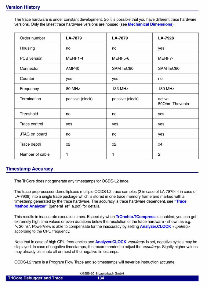
Version History
The trace hardware is under constant development. So it is possible that you have different trace hardware versions. Only the latest trace hardware versions are housed (see Mechanical Dimensions).
Timestamp Accuracy
The TriCore does not generate any timestamps for OCDS-L2 trace.
The trace preprocessor demultiplexes multiple OCDS-L2 trace samples (2 in case of LA-7879, 4 in case of LA-7928) into a single trace package which is stored in one trace memory frame and marked with a timestamp generated by the trace hardware. The accuracy is trace hardware dependent, see “Trace Method Analyzer” (general_ref_a.pdf) for details.
This results in inaccurate execution times. Especially when TrOnchip.TCompress is enabled, you can get extremely high time values or even durations below the resolution of the trace hardware - shown as e.g. "< 20 ns". PowerView is able to compensate for the inaccuracy by setting Analyzer.CLOCK <cpufreq> according to the CPU frequency.
Note that in case of high CPU frequencies and Analyzer.CLOCK <cpufreq> is set, negative cycles may be displayed. In case of negative timestamps, it is recommended to adjust the <cpufreq>. Sightly higher values may already eliminate all or most of the negative timestamps.
OCDS-L2 trace is a Program Flow Trace and so timestamps will never be instruction accurate.
Order number LA-7879 LA-7879 LA-7928
Housing no no yes
PCB version MERF1-4 MERF5-6 MERF7-
Connector AMP40 SAMTEC60 SAMTEC60
Counter yes yes no
Frequency 80 MHz 133 MHz 180 MHz
Termination passive (clock) passive (clock) active50Ohm Thevenin
Threshold no no yes
Trace control yes yes yes
JTAG on board no no yes
Trace depth x2 x2 x4
Number of cable 1 1 2
TriCore Debugger and Trace 134 ©1989-2018 Lauterbach GmbH
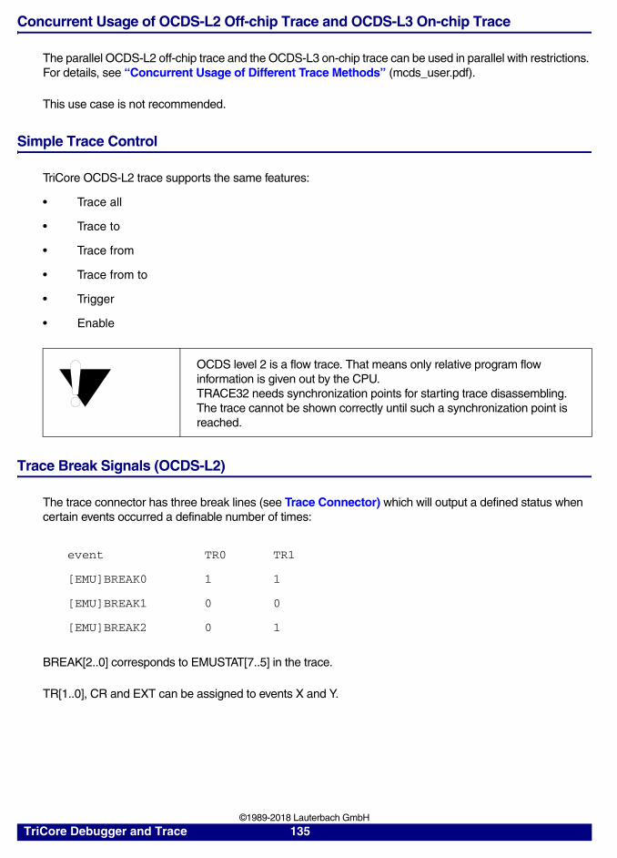
Concurrent Usage of OCDS-L2 Off-chip Trace and OCDS-L3 On-chip Trace
The parallel OCDS-L2 off-chip trace and the OCDS-L3 on-chip trace can be used in parallel with restrictions. For details, see “Concurrent Usage of Different Trace Methods” (mcds_user.pdf).
This use case is not recommended.
Simple Trace Control
TriCore OCDS-L2 trace supports the same features:
• Trace all
• Trace to
• Trace from
• Trace from to
• Trigger
• Enable
Trace Break Signals (OCDS-L2)
The trace connector has three break lines (see Trace Connector) which will output a defined status when certain events occurred a definable number of times:
BREAK[2..0] corresponds to EMUSTAT[7..5] in the trace.
TR[1..0], CR and EXT can be assigned to events X and Y.
OCDS level 2 is a flow trace. That means only relative program flow information is given out by the CPU.TRACE32 needs synchronization points for starting trace disassembling. The trace cannot be shown correctly until such a synchronization point is reached.
event TR0 TR1
[EMU]BREAK0 1 1
[EMU]BREAK1 0 0
[EMU]BREAK2 0 1
TriCore Debugger and Trace 135 ©1989-2018 Lauterbach GmbH
Trace Examples
A successfully loaded target application is needed for the following examples.
Example 1: Trace from
Start recording at address 0xA0001000.
Example 2: Trace to
Stop recording at address 0xA0001100, but do not halt the CPU.
Example 3: Trace from to
Start recording at address 0xA0001000 and stop recording at address 0xA0001100, but do not halt the CPU. If recording was stopped once it will restart when the start address is reached once more.
Trace is just a pointer to the currently selected trace method (see Trace.METHOD).
Analyzer.view ; show trace setup window
Analyzer.Mode STACK ; set trace to stack mode
Analyzer.List ; show trace list window
Break.Set 0xA0001000 /TraceON ; set start address
Analyzer.view ; show trace setup window
Analyzer.Mode STACK ; set trace to stack mode
Analyzer.List ; show trace list window
Break.Set 0xA0001100 /TraceOFF ; set end address
Analyzer.view ; show trace setup window
Analyzer.Mode STACK ; set trace to stack mode
Analyzer.List ; show trace list window
Break.Set 0xA0001000 /TraceON ; set start address
Break.Set 0xA0001100 /TraceOFF ; set end address
TriCore Debugger and Trace 136 ©1989-2018 Lauterbach GmbH
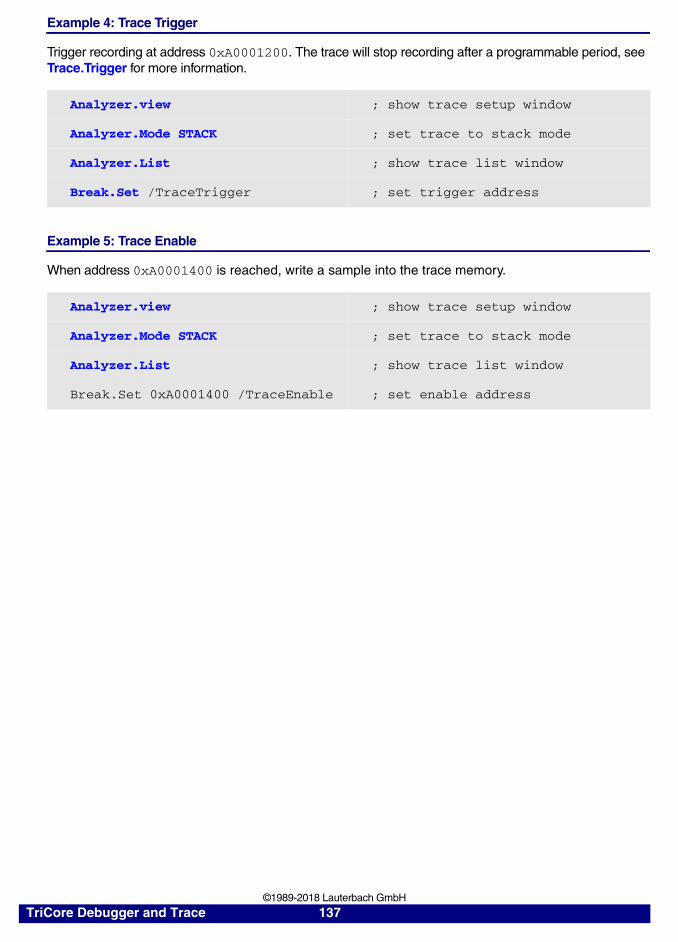
Example 4: Trace Trigger
Trigger recording at address 0xA0001200. The trace will stop recording after a programmable period, see Trace.Trigger for more information.
Example 5: Trace Enable
When address 0xA0001400 is reached, write a sample into the trace memory.
Analyzer.view ; show trace setup window
Analyzer.Mode STACK ; set trace to stack mode
Analyzer.List ; show trace list window
Break.Set /TraceTrigger ; set trigger address
Analyzer.view ; show trace setup window
Analyzer.Mode STACK ; set trace to stack mode
Analyzer.List ; show trace list window
Break.Set 0xA0001400 /TraceEnable ; set enable address
TriCore Debugger and Trace 137 ©1989-2018 Lauterbach GmbH
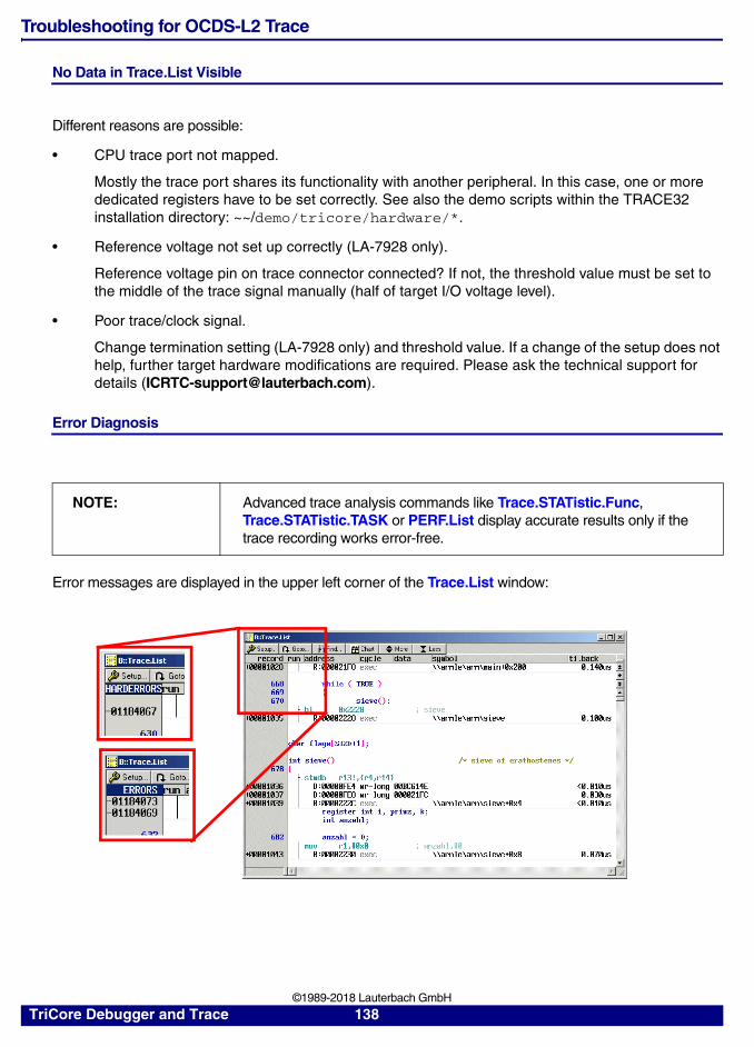
Troubleshooting for OCDS-L2 Trace
No Data in Trace.List Visible
Different reasons are possible:
• CPU trace port not mapped.
Mostly the trace port shares its functionality with another peripheral. In this case, one or more dedicated registers have to be set correctly. See also the demo scripts within the TRACE32 installation directory: ~~/demo/tricore/hardware/*.
• Reference voltage not set up correctly (LA-7928 only).
Reference voltage pin on trace connector connected? If not, the threshold value must be set to the middle of the trace signal manually (half of target I/O voltage level).
• Poor trace/clock signal.
Change termination setting (LA-7928 only) and threshold value. If a change of the setup does not help, further target hardware modifications are required. Please ask the technical support for details ([email protected]).
Error Diagnosis
Error messages are displayed in the upper left corner of the Trace.List window:
NOTE: Advanced trace analysis commands like Trace.STATistic.Func, Trace.STATistic.TASK or PERF.List display accurate results only if the trace recording works error-free.
TriCore Debugger and Trace 138 ©1989-2018 Lauterbach GmbH
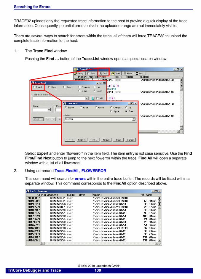
Searching for Errors
TRACE32 uploads only the requested trace information to the host to provide a quick display of the trace information. Consequently, potential errors outside the uploaded range are not immediately visible.
There are several ways to search for errors within the trace, all of them will force TRACE32 to upload the complete trace information to the host:
1. The Trace Find window
Pushing the Find … button of the Trace.List window opens a special search window:
Select Expert and enter “flowerror” in the item field. The item entry is not case sensitive. Use the Find First/Find Next button to jump to the next flowerror within the trace. Find All will open a separate window with a list of all flowerrors.
2. Using command Trace.FindAll , FLOWERROR
This command will search for errors within the entire trace buffer. The records will be listed within a separate window. This command corresponds to the FindAll option described above.
TriCore Debugger and Trace 139 ©1989-2018 Lauterbach GmbH
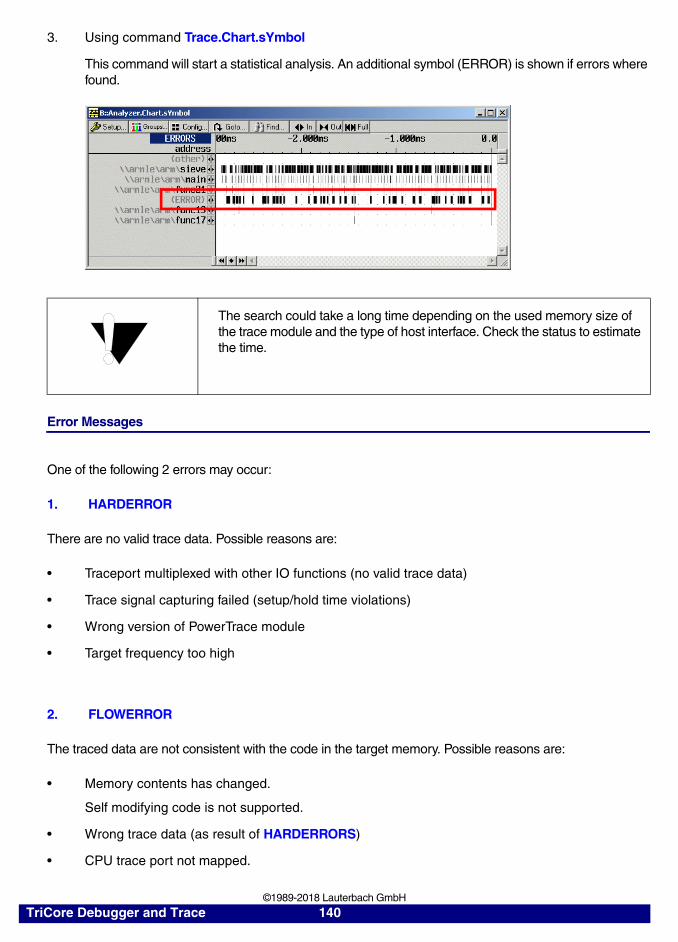
3. Using command Trace.Chart.sYmbol
This command will start a statistical analysis. An additional symbol (ERROR) is shown if errors where found.
Error Messages
One of the following 2 errors may occur:
1. HARDERROR
There are no valid trace data. Possible reasons are:
• Traceport multiplexed with other IO functions (no valid trace data)
• Trace signal capturing failed (setup/hold time violations)
• Wrong version of PowerTrace module
• Target frequency too high
2. FLOWERROR
The traced data are not consistent with the code in the target memory. Possible reasons are:
• Memory contents has changed.
Self modifying code is not supported.
• Wrong trace data (as result of HARDERRORS)
• CPU trace port not mapped.
The search could take a long time depending on the used memory size of the trace module and the type of host interface. Check the status to estimate the time.
TriCore Debugger and Trace 140 ©1989-2018 Lauterbach GmbH
Mostly the trace port shares its functionality with another peripheral. In this case, one or more dedicated registers have to be set correctly. See also the demo scripts within the TRACE32 installation directory: ~~/demo/tricore/hardware/*.
• Reference voltage not set up correctly (LA-7928 only).
Reference voltage pin on trace connector connected? If not, the threshold value must be set to the middle of the trace signal manually (half of target I/O voltage level).
• Poor trace/clock signal.
Change termination setting (LA-7928 only) and threshold value. If a change of the setup does not help, further target hardware modifications are required. Please ask the technical support for details ([email protected]).
• Setup/hold time violation.
- 3 ns setup / 1 ns hold time needed.
- sample point: falling edge.
TriCore Debugger and Trace 141 ©1989-2018 Lauterbach GmbH