Embed Size (px)
Citation preview

Trench Effects in Copper Electroplating
Student: Oleg Gurinovich Industry: Novellus SystemsAdvisor: Dr. Stacy Gleixner John Kelly, Jim Stimmell, Chiu ChiInstructor: Dr. Richard Chung TFI: Bill Gadson
Mate 198B Spring 2001
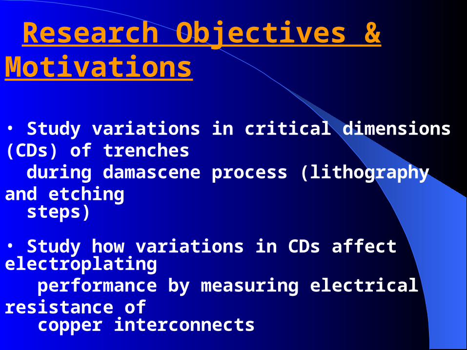
Research Objectives & Motivations
• Study variations in critical dimensions (CDs) of trenches during damascene process (lithography and etching steps)
• Study how variations in CDs affect electroplating performance by measuring electrical resistance of copper interconnects
• More companies switch to copper as a material choice for interconnects
• Strong correlation between to be filled feature size and electroplating bath chemistry
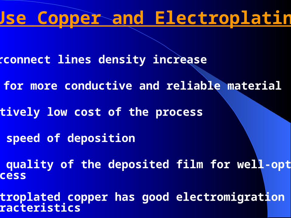
Why Use Copper and Electroplating?
• Interconnect lines density increase
• Need for more conductive and reliable material
• Relatively low cost of the process
• High speed of deposition
• High quality of the deposited film for well-optimized process
• Electroplated copper has good electromigration characteristics
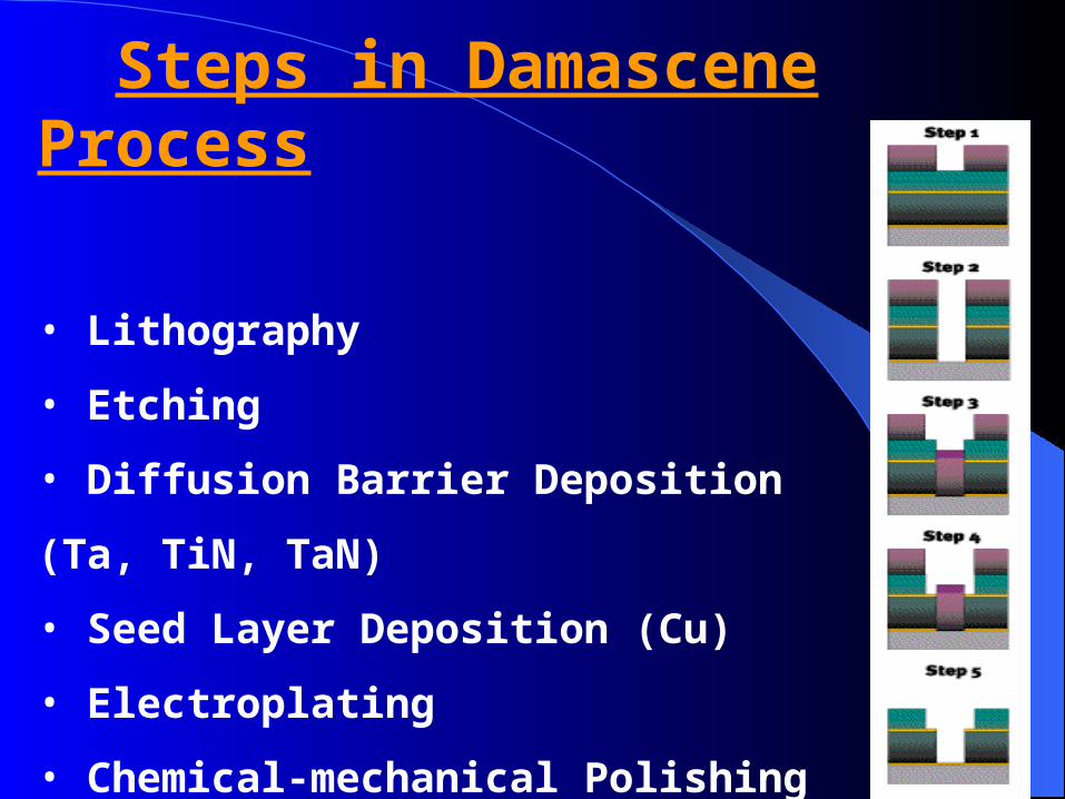
Steps in Damascene Process
• Lithography
• Etching
• Diffusion Barrier Deposition (Ta, TiN, TaN)
• Seed Layer Deposition (Cu)
• Electroplating
• Chemical-mechanical Polishing

Electroplating Scheme
CuSO4+H
2O+H
2SO
4 + additives
Cathode (Wafer):
Cu2+ + e- = Cu+
Cu+ + e- = Cu0
Anode:
4OH-=O2+ 2H
2O + 4e-
2H 2O=O
2+ 2H+ +2e-
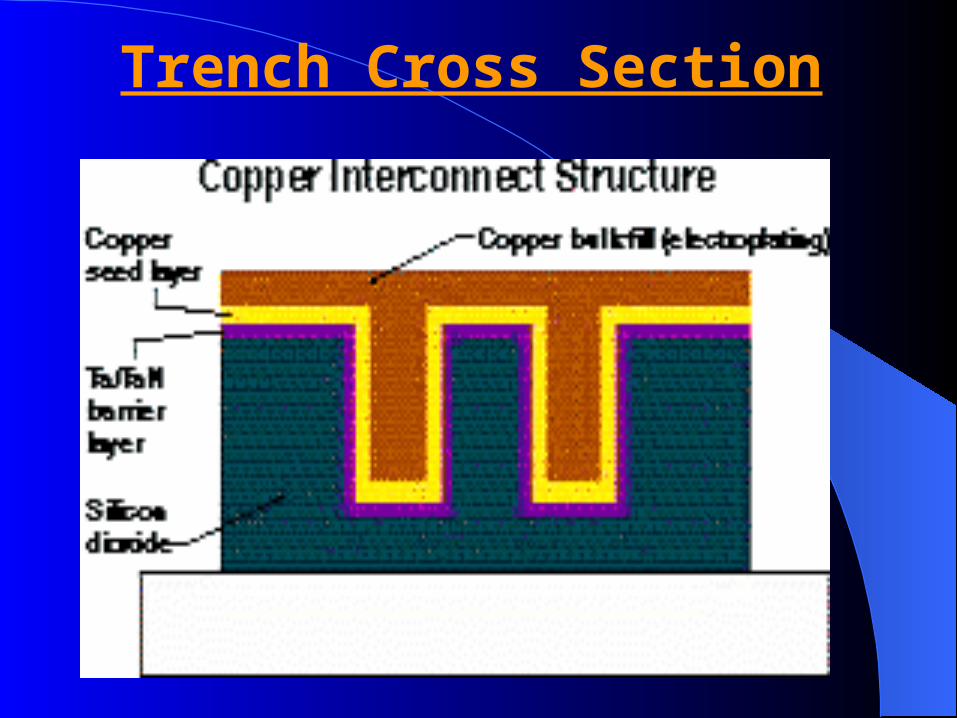
Trench Cross Section
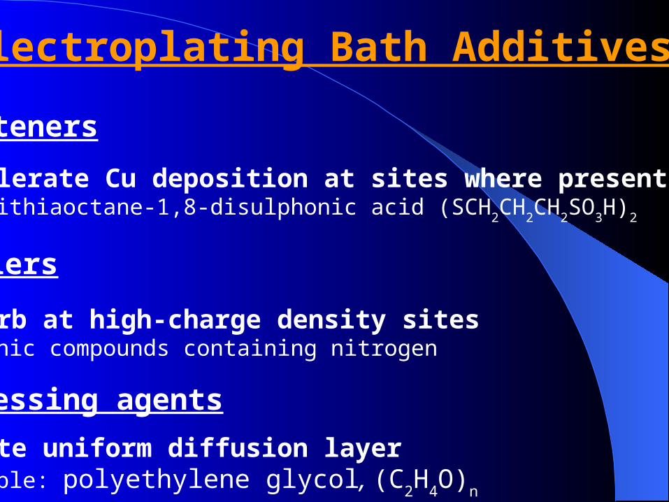
Electroplating Bath Additives
Brighteners
• accelerate Cu deposition at sites where present 4,5-dithiaoctane-1,8-disulphonic acid (SCH
2CH
2CH
2SO
3H)
2
Levelers
• adsorb at high-charge density sites organic compounds containing nitrogen Suppressing agents
• create uniform diffusion layer Example: polyethylene glycol, (C
2H
4O)
n
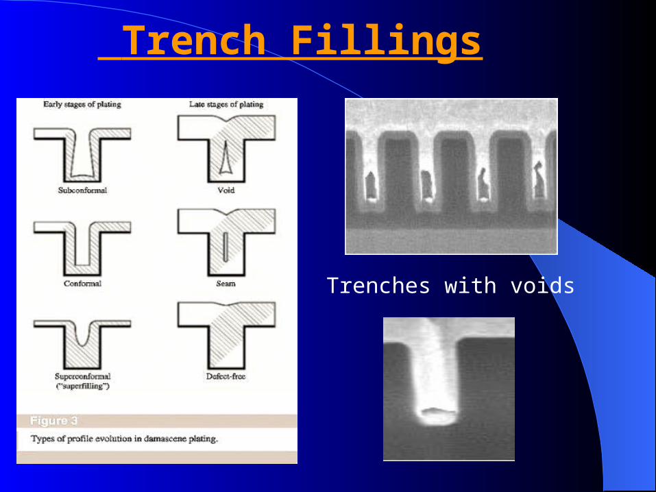
Trench Fillings
Trenches with voids

Experimental Procedure
• Measure width of 0.25 m trenches after lithography and etch steps to find variance in the trench width introduced by these two processes
• Measure electrical resistance of copper interconnects to find how actual trench size variations affect electroplated copper characteristics
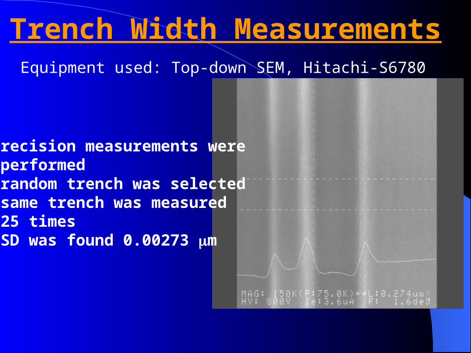
Trench Width MeasurementsEquipment used: Top-down SEM, Hitachi-S6780
• Precision measurements were performed -random trench was selected -same trench was measured 25 times -SD was found 0.00273 m

Lithography defects
Normal trenches Underdeveloped trenches Overdeveloped trenches

Measurements Map
After-lithography measurements After-etch measurements

Trench width distribution, lithography
0.23
0.24
0.25
0.26
0.27
0.28
0.29
0 2 4 6 8 10 12 14 16 1820 22 24 26 28 3032 34 36
Measurement point
Tre
nch
wid
th,
mic
ron
s
Series1
Trench width distribution, etching
0.15
0.16
0.17
0.18
0.19
0.2
0.21
0.22
0 2 4 6 8 10 12 14 16 18 20 22 24 26 28 30
Measurement point
Tre
nch
wid
th,
mic
ron
s
Series1
Measurements Data
Width is distributed around mean value of 0.257 mNo significant trend
Trend is observed, central dies on the wafer have wider trenchesafter etching step

After-etch Measurements MapFour 8-inch wafers were measured
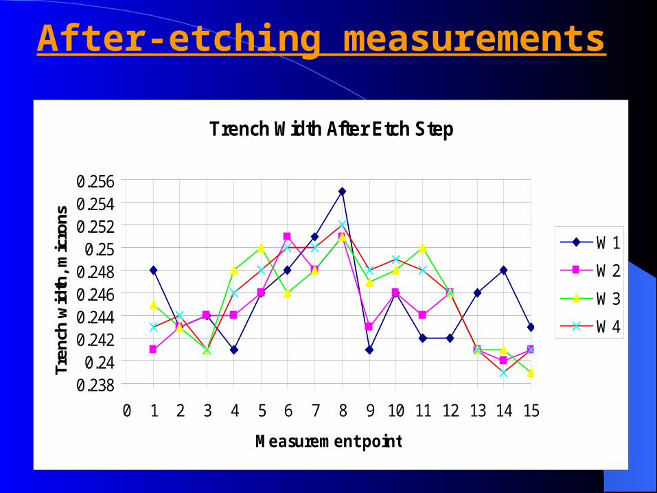
Trench Width After Etch Step
0.2380.240.2420.2440.2460.2480.250.2520.2540.256
0 1 2 3 4 5 6 7 8 9 10 11 12 13 14 15
Measurement point
Tren
ch w
idth
, mic
rons
W1
W2
W3
W4
After-etching measurements

Discussions
• Lithography step doesn’t introduce special cause variation -data distribution does not show significant trend -mean value 0.257 m, SD is 0.0114 m
• Etching step does have special cause variation
-central area of the wafer is etched more than edges -account for this effect during electrical resistance measurements -mean trench width after etching 0.2454 m, SD is 0.00574
• Need to be aware of lithography defects while analyzing resistance data
Conclusions
• Etch step may affect electrical resistance of copper interconnects
• Based on the literature research, bath additives concentrations will affect trench fill capability
• Lithography step do not affect overall trench width distribution
• Measuring procedure (map) is developed
Future Work
• Measure electrical resistance of copper interconnects
• Anneal wafers at different temperatures after electroplating to study effect of annealing on copper grain “re-growth”
• Study effects of electroplating bath chemistry on copper interconnects electrical characteristics