Embed Size (px)
Citation preview

JOURNAL OF LIGHTWAVE TECHNOLOGY, VOL. 16, NO. 12, DECEMBER 1998 2117
Transparent Optical Packet Switching:The European ACTS KEOPS
Project ApproachChristian Guillemot, Monique Renaud, Piero Gambini,Member, IEEE,Christopher Janz,
Ivan Andonovic,Senior Member, IEEE,Raimond Bauknecht, Bruno Bostica, Marco Burzio, Franco Callegati,Maurizio Casoni, Dominique Chiaroni, Fabrice Clerot, Soren Lykke Danielsen, Fran¸cios Dorgeuille,
Arnaud Dupas, A. Franzen, Peter Bukhave Hansen, David K. Hunter,Member, IEEE,Allan Kloch, R. Krahenbuhl,Bruno Lavigne, Alain Le Corre, Carla Raffaelli, Michael Schilling, Jean-Claude Simon, and Libero Zucchelli
(Invited Paper)
Abstract—This paper reviews the work carried out under theEuropean ACTS KEOPS (KEys to Optical Packet Switching)project, centering on the definition, development and assessmentof optical packet switching and routing networks capable ofproviding transparency to the payload bit rate. The adoptedapproach uses optical packets of fixed duration with low bit rateheaders to facilitate processing at the network/node interfaces.The paper concentrates on the networking concepts developedin the KEOPS project through a description of the implemen-tation issues pertinent to optical packet switching nodes andnetwork/node interfacing blocks, and consideration of the net-work functionalities provided within the optical packet layer. Theimplementation, from necessity, relies on advanced optoelectroniccomponents specifically developed within the project, which arealso briefly described.
I. INTRODUCTION
W AVELENGTH division multiplexing (WDM) opticalnetwork concepts provide a platform for significant
improvement in network bandwidth capacity and are poisedto dominate the backbone infrastructure supporting the next-generation high-speed networks (ATM, IP). The rapid increasein traffic levels necessitates networks with fast packet switch-ing, supported by native optical transmission. While current
Manuscript received June 18, 1998. This work supported in part by theEuropean Commission through the ACTS AC043 KEOPS Project.
C. Guillemot, F. Clerot, A. Dupas, A. Le Corre, and J.-C. Simon are withthe France Telecom-CNET, Lannion Cedex F-22301 France.
M. Renaud, C. Janz, and F. Dorgeuille are with OPTO+; Groupementd’Interet Economique, Alcatel Corporate Research Center, Marcoussis F-91460 France.
P. Gambini, B. Bostica, M. Burzio, and L. Zucchelli are with CSELT-CentroStudi E Laboratori Telecomunicazioni, Torino I-10148 Italy.
I. Andonovic, A. Franzen, and D. K. Hunter are with the University ofStrathclyde, Glasgow G1 1XW, U.K.
R. Bauknecht and R. Kr¨ahenbuhl are with the ETH-Swiss Federal Instituteof Technology, Honggerberg, HPT, CH-8093 Zurich, Switzerland.
F. Callegati, M. Casoni, and C. Raffaelli are with the University of Bologna,Bologna I-40136 Italy.
D. Chiaroni and B. Lavigne are with the Alcatel Corporate Research Center,Marcoussis F-91460 France.
S. L. Danielsen, P. B. Hansen, and A. Kloch are with the TechnicalUniversity of Denmark, Lyngby DK-2800 Denmark.
M. Schilling is with Alcatel SEL, Stuttgart D-70435 Germany.Publisher Item Identifier S 0733-8724(98)09299-8.
applications of WDM focus on the static usage of individualWDM channels, optical switching technologies enable the fastallocation of WDM channels in an on-demand fashion withfine granularities (microsecond time scales). The challengenow is to combine the advantages of the relatively coarse-grained WDM techniques with emerging all-optical switchingcapabilities to yield a high-throughput optical platform directlyunderpinning next generation data networks.
In this context, the ACTS KEOPS Project (KEys to OpticalPacket Switching) addresses the analysis and demonstration ofoptical (bit rate) transparent packet (OTP) switching within all-optical network architectures by means of network and systemstudies, and laboratory demonstrators based on componentsdeveloped in the project. Partners contributing to the KEOPSproject are Alcatel Alsthom Recherche (F), France Telecom-CNET (F), CSELT (I), Technical University of Denmark (DK),Alcatel CIT (F), Alcatel SEL (D), University of Bologna (I),ETH-Zurich (CH) and the University of Strathclyde (UK).Progress achieved since the start of the project in September1995, on network and system issues, system demonstratorsand components, is reported in this paper, that is structuredas follows:
In Section II, the main issues with respect to supportingnext-generation high-speed networks are discussed, highlight-ing the benefits afforded by optical packet networking com-bined with WDM techniques. Although the focus is hereput on interworking with IP networks because of the boom-ing deployment experienced by the Internet, the approachapplies also to other high speed networks such as ATM.The required functionalities for interfacing with WDM cross-connected networks are reviewed as well. Section III addressesthe optical node architectures, starting with the identificationof the subblocks necessary for interfacing the switching fabricwith WDM transmission links. Several architectural optionsare examined with the aim of overcoming the limitationsimposed on performance by optical buffering. Section IVsummarizes the development of key technologies and function-alities required not only for the KEOPS demonstrator activitiesbut more significantly, representing a common technology base
0733–8724/98$10.00 1998 IEEE

2118 JOURNAL OF LIGHTWAVE TECHNOLOGY, VOL. 16, NO. 12, DECEMBER 1998
for all WDM optical networks. Finally, an examination of theachievements of the project coupled with a detailed evaluationof the potential of optical packet switching enables a criticalcomparison of the advantages of optical packet networks withrespect to electronic systems (Section V).
II. OPTICAL PACKET NETWORKS: LINKING
WDM AND HIGH-SPEED DATA NETWORKS
A. High Bit Rate Networking
1) Issues: The convergence of telecommunications andcomputer communications has been anticipated for sometime since both rely on the underlying digital technology.In the early 1980’s, the scenario appeared relatively clearcut: traditional telecommunications traffic was dominant andachieving the integration meant upgrading the connectionoriented, circuit-switched telecommunications infrastructure toenable the support of data traffic. Entering the new millenium,the networking environment has completely changed.
• The current trend for data traffic transmission worldwide,in particular of Internet traffic, shows that, in the midterm,it will reach and even exceed traffic due to telephonyservice, making data communications the dominant traffictype [1].
• The development of WDM techniques on point-to-pointlinks utilizes the optical bandwidth of installed fibers ef-ficiently and incrementally (with respect to the number ofwavelength channels as well as the bit rate per channel).
• The future development of optical cross-connected WDMtransport networks, dynamically managing optically trans-parent lightpaths, will potentially render redundant thenetwork functionalities provided by the SDH layer.
• From the client perspective, IP has become the dominantprotocol for data communications; it thus represents avery strong candidate for the integration of data communi-cations with telecommunications. Even if present versionsof IP cannot support differentiation of the client flowson quality-of-service (QoS) criteria, ongoing develop-ment within the Internet Engineering Task Force (IETF)should soon result in advances capable of guaranteeing asufficient QoS across a spectrum of traffic types.
Thus, within the last two decades, the accepted vision ofthe Broadband Integrated Service Digital Network architecture(BISDN) has widened and now encompasses IP/WDM inaddition to ATM/SDH or IP/SDH/WDM.
The main concern with the IP/WDM approach is the mis-match between the transmission capacities offered by theWDM optical layer and the processing power of current routers[2]. IP routers perform three main tasks:
1) routing: supporting various protocols so as to maintainthe network connectivity information contained in therouting tables;
2) forwarding: referring to the routing table for each incom-ing packet to determine the output interface to which thepacket should be written;
3) switching: directing each packet to the proper outputinterface, as defined by the forwarding process.
With respect to routing, the main issues stem from the sizeof the routing tables and the frequency of their updates.Such problems are currently addressed and managed by well-known means (route aggregation, routing protocol updatingto avoid redundant or obsolete information exchanges). Themain performance bottleneck arises at the forwarding level.The time needed for a routing table look-up sets a hard limitto the router throughput (expressed in packet/s). Two differentsolutions have been proposed to alleviate this bottleneck [3],[4]: 1) parallelization of the forwarding operation, as this isperformed independently on packet-by-packet basis and 2)optimization of the routing table encoding and of the look-upalgorithm, resulting in impressive improvements. Consideringa conservative estimate of the average packet size of 200 byteswith a pessimistic evaluation of look-ups per second,demonstrated on 200 MHz Pentium Pro platform, the limit onthe maximum bit rate set by the forwarding process is about3 Gb/s.
The adoption of current ATM switching technology orswitching technologies inherited from the supercomputer in-dustry provide access to large and fast switching matrices,which might alleviate the switching bottleneck. Advances intechnology and architectures have lead to a new generationof IP gigabit routers, a prime example being the Neo Net-works 512 Gb/s nonblocking switching matrix for its streamProcessor 2400 [5].
Despite these impressive upgrades, it should neverthelessbe noted that electronic switching systems lack flexibilityregarding their throughput upgrade capability. Given thatWDM allows cheap incremental increases of the transmissionbandwidth, much more frequent upgrades of the transport layercapacity can be envisaged to match increasing demand. Suchfrequent increases will place heavy demands on the switchingprocess, which in turn will require frequent, costly upgradesto keep up with the transmission rate.
2) Optical Packet Networking:Given the above trends,KEOPS seeks to combine packet switching with WDMtransmission techniques to yield WDM optical packetswitching. The goal is to shift most of the switching burdeninto the optical domain, permitting the successful scaling ofthe switching capability of IP routers, compatible with thecapacity of WDM transmission. In so doing, an effectivedecoupling between the bandwidth and routing/forwardingis also achieved. The former, involving both transmissionand switching, is addressed in the optical domain, accessingthe huge fiber bandwidth; the latter is carried out in theelectronic domain, where the relatively complex packetrouting/forwarding process occurs at the packet header levelwhatever the size of the attached data entity.
In addition, the optical packet layer provides some basiclink layer functions mandatory for efficient interfacing of IPwith the WDM layer by transporting IP packets in opticalpacket payloads. It also provides a further multiplexing levelin the time domain, necessary to allow the IP routers toaggregate client flows prior to transmitting information ontothe optical WDM pipe. This generally removes the needfor SDH as an adaptation layer for IP traffic on point-to-point WDM wavelength channels. This trend is reinforced

GUILLEMOT et al.: TRANSPARENT OPTICAL PACKET SWITCHING 2119
Fig. 1. Packet format used within KEOPS project.
by recent initiatives which aim to overlay switching androuting technologies directly onto optical networks [6]. Suchinitiatives imply the realization of a clear-channel 2.5 Gb/sinterface between IP gigabit routers and long-haul WDMsystem, eliminating the need for SDH terminal multiplexers orother intermediate network elements. Such an interface wouldallow the entire 2.5 Gb/s bandwidth of an STM-16 connectionto be treated as a single, dark fiber pipe.
Furthermore, the decoupling of the transmission and switch-ing requirements from the routing/forwarding functionalities,highlights optical packet networking as a promising candidateable to support any dedicated electronic routing/forwardingnetworking protocols while exploiting the bandwidth of opticalfibers. Considering that core routers experience heavy trafficconditions in IP backbones, alleviating the load placed onthe forwarding processors remains a crucial goal. Solutionsbased on label switching are currently being considered withinthe multiprotocol label switching (MPLS) framework [7] tobypass the forwarding bottleneck. The emergence, therefore,of a solution providing connection-oriented networking capac-ities, flexible in term of bandwidth management and futureproof with regard to bandwidth growth, is much sought after.KEOPS also provides interconnection facilities through theoptical packet networking.
A number of approaches exist for realising optical trans-parent packet networks (OTP-N) [8]. In the case of theKEOPS optical transparent packet network, fixed durationpackets are utilized where both the header and its attachedpayload are encoded on the same wavelength carrier. Routinginformation is derived from the packet header after opto-electronic conversion; the header is encoded at a low fixedbit rate, e.g., 622 Mb/s, to allow the utilization of standardelectronic processing. In order to realize a network insensitiveto the load bit rate, the payload duration is fixed whatever itscontent; the data volume is proportional to the user-defined bitrate which may vary from a few hundred Mb/s to 10 Gb/s, witheasy upgrade capability [9]. The packet format is depicted inFig. 1.
B. Optical Transparent Packet Network Architecture
1) Interworking with Electronic Networks and WDM Trans-port Networks: In this section, the architecture for the OTP-Narchitecture is described when, consistent with the scenariooutlined in the previous section, the traffic is predominately IP.The OTP-N is seen as a very high-capacity transport facility,able to switch and transport traffic flows made of aggregated IPdatagram streams. Access to the OTP-N is provided by high-
Fig. 2. Connection of IP networks by means of the OTP-N.
Fig. 3. OTP-N network reference structure.
speed IP routers, with optical packet interfaces, subsequentlyreferred to as edge routers (Fig. 2). The purpose here isto highlight the functions required in the edge routers aswell as the architecture and protocol layering of the accessinterfaces to the OTP-N (OTP interworking unit or IWU). TheOTP access interface has been subdivided into four sublayers(Fig. 3).
• The data convergence sublayer (DCSL) is responsible fordata rate adaptation, encapsulating incoming IP datagramsinto optical packets. Given variable length datagrams,it is assumed that no fragmentation or reassembly isperformed in the OTP layer; the maximum length ofIP datagrams that can be carried in the OTP-N is setby the OTP length and by the link bit rate. Longer IPdatagrams will be segmented by the router accordingto the IP protocol specification (adding the proper IPheader). At the same time short IP datagrams, addressedto the same subnetwork, can be multiplexed on the sameOTP, in order to achieve maximum payload usage, butagain without any processing of the IP header.
• The network sublayer (NSL), below the DCSL, is re-sponsible for generation of the OTP routing label/address,inserted in the OTP header. Presently, it is assumedthat a unique OTP label/address is assigned to eachDCSL. Therefore the conventional part of the router isresponsible for forwarding the IP datagrams to the properDCSL according to their final subnetwork destination.
• OTP’s from/to different DCSL/NSL pairs are mutli-plexed/demultiplexed in the link sublayer (LSL), forinstance by means of a simple FIFO queue, and then

2120 JOURNAL OF LIGHTWAVE TECHNOLOGY, VOL. 16, NO. 12, DECEMBER 1998
(a)
(b)
Fig. 4. Example of packet delivery at the edges of the OTP-N accordingto the (a) wavelength circuit and (b) wavelength packet option. Packetsof different colors belong to different connections. Different line-styles aredifferent wavelengths.
transmitted as a unique packet stream. Note that opticalidle packets may be inserted by the LSL to keep thetransmitted optical power constant. Empty packets can bediscarded at any time in the network and can therefore beneglected as far as teletraffic performance is concerned.
• Proper wavelength encoding for transmission in theoptical fiber—taking into consideration the use of thewavelength resource (see Wavelength Managementbelow)—is provided by the wavelength convergencesublayer (WCSL).
2) Wavelength Management:The wavelength resource canbe exploited both within the network nodes and in the networklinks. In the switching fabric, the wavelength dimension isused for routing and internal contention resolution, in con-junction with the space dimension. This use of wavelengthis strictly internal to each switch and does not impinge onnetwork issues, assuming the switch outputs conform to thetransmission requirements of the links (output wavelengthconversion interfaces will be provided if needed).
With respect to the links between nodes, two options havebeen considered up to now within the KEOPS project for theuse of the wavelength domain.
• The wavelengths are taken as circuits and the elementarypaths within the network are designated by the wave-length and not the fiber. Thus, packets belonging to agiven connection cannot be spread over more than onewavelength per hop. This will be calledwavelength circuit(WC).
• The wavelengths of a fiber can be used as a sharedresource. Traffic load is spread over the wavelength setand packets belonging to the same connection can betransmitted on different wavelengths in the same hop.Paths within the network are associated with fibers andwavelengths. This will be calledwavelength packet(WP).
Fig. 4(a) shows how each connection makes use of onewavelength only (one logical buffer per wavelength), an ex-ample of WC operation. Packets of a given connection re-main strictly in sequence and are transmitted on one single
wavelength. Interfacing with the WDM transport layer isrelatively straightforward, although wavelength reallocationmight be necessary depending on the set of wavelengthsused (not necessarily in accordance with the set used in thetransport layer). In general, this reallocation is required sincethe wavelength allocation for the provision of end-to-endlightpaths is purely a WDM transport layer concern.
If packets are statistically multiplexed over the wavelengthset, bursts of packets can be served more easily as they contendonly for their output fiber with a significant reduction in thebuffering requirement in switches [Fig. 4(b)]. The drawback,however, is the necessity to properly demultiplex the packetflows carried by a given fiber in the wavelength domain, atOTP-N edges. This operation involves packet queuing andis dealt with by the edge switches comprising full opticalpacket switches, with as many outgoing ports as wavelengthchannels utilized in carrying the fiber packet stream. Edgeswitches are a strict requirement at the IWU’s for interfacingwith electronic IP subnetworks. They might also be neededat interfaces with the underlying WDM transport networkif the transmission capacities allocated by the WDM layerare treated as independent wavelength channels. In case ofinterconnection capacities scaled over several wavelengths,blind striping of the traffic by IP routers on lightpaths withdifferent delays would result in massive disordering of packetsand poor end-to-end performance. With respect to transportingpacketized data, WDM transport networks should take intoaccount such delay requirements in their wavelength pathmanagement (also true for lightpath allocation in case offailure) as soon as the client network (IP or future OTP-Ns)asks for a bandwidth capacity exeeding that of a wavelengthchannel.
Both options have advantages and drawbacks and the se-lection of the best approach is a tradeoff between complexityand performance, highly dependent on the application environ-ment. However, the two solutions are not mutually exclusiveand can coexist with the correct interfacing blocks.
III. OPTICAL PACKET SWITCHING NODES
The KEOPS project has generated several new approachesto realising optical packet nodes. The node, which fulfills themost important function in a network, i.e., the distribution ofinformation to the right destinations, has to incorporate a num-ber of functionalities, some of them executed in the electronicdomain while others resort to optical signal processing. Therelationships between these functionalities are outlined for ageneric node structure consisting of the following subblocks:
• the input interface, incorporating a synchronization func-tion;
• the switching fabric;• the output interface incorporating regeneration and header
rewriting.
In this section, the focus is on the core of the node, theswitching fabric. The two main architectural options consid-ered within the KEOPS project for the implementation of thebasic switching blocks are examined in details. Implementa-

GUILLEMOT et al.: TRANSPARENT OPTICAL PACKET SWITCHING 2121
Fig. 5. Generic node structure.
Fig. 6. Schematic of the wavelength routing switch. TOWC stands for tuneable optical wavelength converter, SOA for semiconductor optical amplifier (crossgain wavelength conversion) and IWC for interferometric wavelength converter (cross gain/phase wavelength conversion).
tion requirements for the input and output interfaces will bepresented in the next section.
Attaining the buffer depths required in practice for con-tention resolution is a fundamental difficulty with all opticalpacket switch designs. Therefore, several realizations of high-performance switch architectures, derived from basic buildingblocks while minimizing the complexity of the optical buffer-ing function, have been developed.
A. Node Architecture
1) Generic Node Structure:The generic structure of an op-tical packet switching node is depicted in Fig. 5. In WDMnetworks, nodes are flanked by passive de/multiplexers, theswitching process being carried out at the packet level perwavelength and per time slot. As a result, the number of portsis scaled according to the number of interconnected fiberstimes the number of multiplexed wavelengths, leading to largeswitching matrices.
As in electronics, interfaces are necessary for reliable in-formation exchange and are just as crucial in optical systems.The input interface aligns the incoming cell streams relativeto the switch master clock, creating synchronous packet flowswhile properly recovering the header content. The outputinterface ensures that physical transmission constraints are
met, including power levels, wavelength allocation, signalshaping and reinsertion of updated headers.
In any end-to-end connection, the payloads are never elec-tronically recovered, necessitating the use of optical synchro-nizers to align the payload time position while maintainingtransparency. Implementing the required payload delineationblocks after the fiber delay line set takes into account thetime jitter undergone by packets within the switching fabric.A pointer field in each header flags the position of the payloadrelative to its header. Rewriting headers synchronously at thestart of each time slot ensures some framing on wavelengthpipes.
2) Switching Matrices:a) Wavelength routing switch (WRS):The first architec-
tural option investigated within KEOPS relies on the wave-length dimension to execute switching by means of tuneableoptical wavelength converters (TOWC’s) (Fig. 6). Delay lines,used for contention resolution, are grouped in several sets andconstitute the first stage of the optical switch. Each input porthas access to, at least, one line in each set of the first stageand each set of delay lines has also access to each output port,which means that each delay line is thus shared by every outputport. A packet arriving on a given input port and directed to agiven output port is routed on one of the available delay lines,given that a delay line of durationis considered available if:

2122 JOURNAL OF LIGHTWAVE TECHNOLOGY, VOL. 16, NO. 12, DECEMBER 1998
Fig. 7. BER penalty and signal waveforms at the WRS output. Conversionfrom �3 = 1542 nm to�1 = 1534 nm at the first stage and from�1 to �i
at the second stage (Mach–Zehnder IWC). Payload bit rate: 2.5 Gb/s.
1) no packet is scheduled intime slots on the appropriateoutput port;
2) no packet is scheduled in time slots on any of thedelay lines leading to the same second stage TOWC;
3) no packet issued from the same input port and targettingthe same output port is scheduled intime slots with
.
Of the available delay lines, the shortest delay is chosen.This scheduling process is greatly improved by proper
distribution of the fiber line lengths. For each input port, nearlyoptimum output queueing performance is achievable by usingonly a restricted set of fiber lines with non consecutive delays[10]. As an example, under regular and balanced input trafficconditions, the packet loss rate is kept in the 109 range fora traffic load below 0.8 for a 16 16 switch, although eachinput port is given access to only 16 delay lines [11], [12](note that, under similar conditions, the packet loss rate isabout 10 4 for output buffers built with 16 fiber lines withconsecutive delays).
When using dynamic (on a packet-by-packet basis) wave-length conversion to route packets, the signal extinction ratiodegradation is critical with respect to the number of nodesa signal can cross while allowing successful recovery ofthe data. Therefore, interferometric wavelength converters areimplemented at the second stage of the switch to achievesignal regeneration prior to transmission to the next node(Fig. 7). A fully equipped 4 4 WRS demonstrator has beenrealized. Wavelength conversion over 12 nm and between fourchannels nm)has been demonstrated. Each input has a real time headerrecovery facility operating at 622 Mb/s [13] while a controlunit manages the fiber delay line allocation according tothe scheduling process. Finally, dummy packets within theincoming streams are erased by the first stage wavelengthconverters to relax the unnecessary occupancy demands onthe delay line buffer. New dummy packets are generated atthe second stage (both payloads and headers are encoded at622 Mb/s) to keep the optical power constant on the outgoinglinks.
Fig. 8. Schematic of broadcast and select switch.
Fig. 9. Physical performance of the 16� 16 broadcast and select switchingmatrice at 10 Gb/s.
b) Broadcast and select switch (BSS):The second archi-tectural option exploits WDM to upgrade the internal through-put of the switch, thus easily achieving pure output queuingand hence optimal delay/throughput performance. Theswitch consists of three sections: thewavelength encoder,the buffer and broadcast section, and thewavelength selectorblock (Fig. 8). The wavelength encoding blockconsists of
wavelength converters, one per input. Each one encodesits packets on a fixed wavelength. Thecell buffer blockcomprises K fiber delay lines followed by a space switch stage,realized using clamped-gain semiconductor optical amplifiers(CG-SOA’s) operating as fast gates. The CG-SOA’s selectpackets from the correct delay lines and send them to thecorrect outputs under electronic control. The last block, thewavelength selector block, consists of demultiplexers whichforward the different outputs to SOA gates before the signalsare recombined, thus selecting packets from the correct inputs.
The broadcasting principle makes a copy of each packet atany delay, enabling the flexible management of the bufferedpackets flows. A copy is also available at each output, sothat this architecture easily supports multicasting, an attractivecapability for future applications.
BER results are reported on Fig. 9 for a test bed consistingof a 16 16 BSS matrix operating at 10 Gb/s. The sensitivitypenalty is below 1 dB with respect to the back-to-backconfiguration.
B. Contention Resolution
Given the basic switching blocks depicted above, severalways to improve the queuing process have been investigated,

GUILLEMOT et al.: TRANSPARENT OPTICAL PACKET SWITCHING 2123
Fig. 10. Cell loss performance of the tandem solution as a function of thebuffer length, obtained by analysis and simulation compared with the singlebroadcast and select switching element with threshold at 85% of the buffercapacity.
keeping the number of delay lines accessed by input portsunchanged (low) because of technological constraints. In thisrespect, whether or not contentions are resolved with the helpof differentiated wavelength encoding is a key consideration.
1) Collision Avoidance in the Time Domain:The follow-ing architectures are intended either for edge switches(controlling the demultiplexing of packet streams carried on aWDM multiplex) or for core switches interconnected througha WDM transport network over geographical distances (inthat case, it is assumed that the traffic is smooth enough tobe considered Bernoulli-like due to traffic smoothing at theborders and/or to a high level of aggregation).
a) Flow control algorithms for improved traffic perfor-mance: Buffer limitations can partly be overcome by cascad-ing two BSS switching elements in tandem with a suitablecontrol procedure [14]. During normal operation the firstswitch stores packets using a round robin mechanism, whilethe second switch stores packets according to their addresses.When a buffer of the second stage exceeds a certain threshold,a buffer in the first stage is dedicated to that destination toincrease the total buffer capacity. Thus, the two buffers behavelike a single, longer buffer with a capacity approximately givenby the sum of the two. The cell loss performance enhancementin the case of random traffic is presented in Fig. 10.
The well-known approach of using several stages of smallerswitches to implement larger fabrics is attractive given thelimited monolithic switch matrix sizes possible with presenttechnology [15]. Therefore, multistage switches, realized byadopting a three-stage Clos architecture, have been studied.For these architectures, especially, interstage flow controltechniques effectively reduce packet loss. Due to the discrete-time nature of the switch, a full buffer in a switching stagecan only accept one packet from the previous stage. With flowcontrol a signal is sent back to the previous stage to stop allbut one incoming packets being directed to the full buffer: tominimize the overall packet loss, the selection of this packetis made on a first-come-first-served principle [16]. The benefitof the flow control policy is shown in Fig. 11. A packet lossprobability of 10 10 is reached with only 23 packet positionsper optical buffer, well within technological limits (32).
Fig. 11. Cell loss performance of a three-stage Clos configuration as afunction of the buffer length, obtained by simulation with and without flowcontrol.
Fig. 12. SLOB architecture; each stage is a modified broadcast and selectswitch (SE or switch element).
b) The SLOB architecture:An alternative to realisinga switch with a greater buffer depth through cascadingmany small switches is the switch with large optical buffers(SLOB’s) [17] (Fig. 12). Choosing the BSS as the basicelement, although other switches could be used, SLOBhas m inputs and outputs. The delay line lengths increaseexponentially from left to right along the structure, and eachbuffer has a depth of packets, where is the numberof stages in the architecture; hence the number of stagesincreases with the logarithm of the buffer depth and emulatesan output-buffered switch.
c) Switch with recirculating ports:The ability of opticalswitches to resolve contentions can also be improved byadding recycling ports to standard architectures, i.e., additionaloutput ports are looped back to the corresponding inputports. This architectural option enables packets to be launchedseveral times through the switching fabric, thus giving riseto queuing delays larger than the longest delay line. Note,however, that the recirculating scheme does not allow forinfinite queuing delays, the number of queuing packets beingbounded by the number of packets that can be simultaneouslymanaged within the switch. Although the standard WRSarchitecture performs well under Bernoulli traffic conditions[11], the packet loss rate cannot be kept low under burstytraffic (Fig. 13). With 16 additional recycling ports, availablequeuing delays extend one order of magnitude beyond the
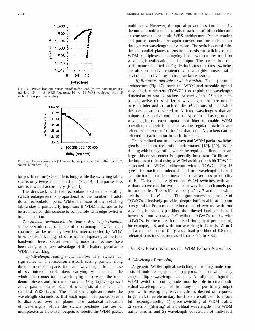
2124 JOURNAL OF LIGHTWAVE TECHNOLOGY, VOL. 16, NO. 12, DECEMBER 1998
Fig. 13. Packet loss rate versus on/off traffic load (source burstiness: 10):standard 16� 16 WRS (squares), 16� 16 WRS equipped with 16recirculation ports (triangles).
Fig. 14. Delay access rate (16 recirculation ports,ON–OFF traffic load: 0.7,source burstiness: 10).
longest fiber line ( 50 packets long) while the switching fabricsize is only twice the standard one (Fig. 14). The packet lossrate is lowered accordingly (Fig. 13).
The drawback with the recirculation scheme is scaling;switch enlargement is proportional to the number of addi-tional recirculation ports. While the issue of the switchingfabric size is particularly important if WDM links are to beinterconnected, this scheme is compatible with edge switchesimplementation.
2) Collision Avoidance in the Time Wavelength Domain:In the network core, packet distribution among the wavelengthchannels can be used by switches interconnected by WDMlinks to take advantage of statistical multiplexing at the fiberbandwidth level. Packet switching node architectures havebeen designed to take advantage of this feature, peculiar toWDM networking.
a) Wavelength routing switch version:The switch de-sign relies on a connection network sorting packets alongthree dimensions: space, time and wavelength. In the caseof interconnected fibers carrying channels, thewhole interconnection network lying in between the inputdemultiplexers and the output couplers (Fig. 15) is organizedas parallel planes. Each plane consists of thestandard WRS fabric. The input demultiplexers route thewavelength channels so that each input fiber packet streamis distributed over all planes. The statistical allocationof wavelengths within the switch precludes the use ofmultiplexers at the switch outputs to rebuild the WDM packet
multiplexes. However, the optical power loss introduced bythe output combiners is the only drawback of this architectureas compared to the basic WRS architecture. Packet routingand packet queuing are again carried out for each packetthrough two wavelength conversions. The switch control rulesthe parallel planes to ensure a consistent building of theWDM multiplexes on outgoing links, without any need forwavelength reallocation at the output. The packet loss rateperformance reported in Fig. 16 indicates that these switchesare able to resolve contentions in a highly bursty trafficenvironment, obviating optical hardware issues.
b) Broadcast and select switch version:The proposedarchitecture (Fig. 17) combines WDM and tuneable opticalwavelength converters (TOWC’s) to exploit the wavelengthdimension for storing packets. At each of the fiber inletspackets arrive on different wavelengths that are uniqueto each inlet and at each of the outputs of the switchthe packets are converted to fixed wavelengths that areunique to respective output ports. Apart from having uniquewavelengths on each input/output fiber to enable WDMoperation, the switch operates as the regular broadcast andselect switch except for the fact that up to packets can beselected at each output in each time slot.
The combined use of converters and WDM packet switchesgreatly enhances the traffic performance [18], [19]. Whendealing with bursty traffic, where the required buffer depths arelarge, this enhancement is especially important. To illustratethe important role of using a WDM architecture with TOWC’scompared to a WDM architecture without TOWC’s, Fig. 18gives the maximum tolerated load per wavelength channelas function of the burstiness for a packet loss probabilityof 10 10. Results are given for WDM switches with andwithout converters for two and four wavelength channels perin- and outlet. The buffer capacity is 7 and the switchsize is 4 4 . The figure shows that the use ofTOWC’s effectively provides deeper buffers able to supportbursty traffic: For a moderate burstiness of two and with fourwavelength channels per fiber, the allowed load per channelincreases from virtually “0” without TOWC’s to 0.4 withTOWC’s. Furthermore, for a fixed throughput per fiber of,for example, 0.8, and with four wavelength channels (and a channel load of 0.2 gives a load per fiber of 0.8), thetolerated burstiness is increased from1.1 to 3.2.
IV. K EY FUNCTIONALITIES FOR WDM PACKET NETWORKS
A. Wavelength Processing
A generic WDM optical switching or routing node con-sists of multiple input and output ports, each of which maycarry multiple wavelength channels. A fully reconfigurableWDM switch or routing node must be able to direct indi-vidual wavelength channels from any input port to any outputport, while reassigning wavelengths as desired or required.In general, three elementary functions are sufficient to ensurefull reconfigurability: 1) space switching of WDM traffic,2) selection (filtering) of individual wavelengths in a WDMtraffic stream, and 3) wavelength conversion of individual

GUILLEMOT et al.: TRANSPARENT OPTICAL PACKET SWITCHING 2125
Fig. 15. WDM architecture version of the WRS.
Fig. 16. Packet loss rate for a WDM WRS interconnecting four fibers car-rying 16 channels; Bemoulli traffic: squares;ON–OFFtraffic (source burstiness:10): triangles.
data channels. These functions represent a shared requirement(and hence potentially a common technology base) for opticalcross-connected networks and packet switching applications,although the required time scale for reconfigurability is ob-viously much smaller in the case of packet switching. Notethat the buffering operation required for packet switchingdoes not introduce any additional elementary functions, as theoptical packet switch architectures described in the previoussection use space switching among fiber delay lines to achievecontention resolution.
1) WDM Space Switching:Many types of optical switches(e.g., optomechanical) can be used for WDM space switching.However, the nanosecond reconfiguration times required foroptical packet switching mandate the use of optoelectronicdevices, which of course have the further advantages ofsmall size and integration potential. These latter considerationsbecome increasingly important, from practical and economicalviewpoints, as larger node dimensions are considered. This istrue for routing as well as packet switching applications.
In the broadcast and select switch architectures studiedwithin KEOPS, space switching is achieved by means of tree-type (perfect shuffle) gated network structures, which allowany connection in a strictly nonblocking mode. Given the re-quirement for fast reconfigurability, semiconductor optical am-plifiers (SOA’s) are perhaps the best available optical gates foruse in such architectures. They can achieve highON–OFF ratios(in excess of 45dB with moderate bias current modulation),which are essential to prevent the build-up of interferometriccrosstalk products, and offer optical gain to at least partially
offset the splitting losses inherent in tree architectures. Theprimary disadvantage of SOA’s is the fast saturation responseof the gain medium to varying optical powers, which makesamplitude-modulated signals subject to distortion at high SOAinput power levels. This limits the useful power dynamicrange of the SOA, and introduces cross-channel modulationdistortion products when gating WDM signals. An effectiveresponse to this problem is the introduction of wavelength-selective optical feedback in the SOA cavity, which introducesa gain-clamping laser oscillation above a certain bias currentthreshold. As long as the total injected optical signal power isinsufficient to extinguish the laser oscillation through carrierdepletion, amplification of arbitrary numbers of wavelengthchannels can be achieved without introducing interchannelcrosstalk. Polarization-insensitive clamped-gain SOA’s (CG-SOA’s) based on bulk-tensile InGaAsP/InP structures withDBR reflectors (oscillation at 1510 nm) have been fabri-cated within the KEOPS project for application as gates;see Fig. 19(a). Experiments on these devices verified a totalpower dynamic range (for 1 dB sensitivity penalty) of 6 dBin 16 WDM channel, 10 Gb/s per channel operation [20]. Todemonstrate the integration potential of the technology, fullypackaged arrays of four such devices have been realized whichexhibited constant fiber-to-fiber gains in excess of 10 dB toinput powers of over 0 dBm, with good uniformity (0.6 dBgain variation) between devices; see Fig. 19(b). Subnanosec-ond gating times were demonstrated on such CG-SOA arraymodules using dedicated high-speed InP HBT driver circuitsdeveloped within the project [21].
Electrooptic switches are a possible alternative to CG-SOA gates for WDM switching applications, and are alsopursued within the KEOPS project. Electrooptic switches arepotentially fast (sub-ns reconfiguration possible), and unlikeSOA gates, they pass or switch signals essentially withoutdistortion over a large power range, and furthermore add nooptical noise. They therefore offer a very large effective powerdynamic range and are virtually free of interchannel modula-tion distortion effects. However, very highON–OFF ratios (40dB or more) are difficult to achieve. Nevertheless, substantialprogress on electro-optic switches has been achieved withinthe project. Polarization-independent InGaAsP/InP switch ma-trices with four 2 2 Mach–Zehnder electrooptic switcheswere fabricated which exhibited fiber-to-fiber insertion lossesas low as 5 dB, switching times below 200 ps andON–OFF
ratios of 30 dB in dilated (cascaded switch) configurations[22].

2126 JOURNAL OF LIGHTWAVE TECHNOLOGY, VOL. 16, NO. 12, DECEMBER 1998
Fig. 17. WDM architecture version of the BSS. The switch hasM fiber in- and outlets withN wavelengths on each. The buffer has a capacity ofB
fiber delay-lines. The length of each fiber delay-line corresponds to a multiple of packet periods,T .
Fig. 18. Highest acceptable channel load (@ PLR=10�10) versus bursti-ness for WDM switch architectures with and without tuneable optical wave-length converters (TOWC). The switch size is 4� 4 and the buffer capacityis seven fiber delay lines.
2) Wavelength Selection:The wavelength selection func-tion, as implemented within the KEOPS packet switch archi-tectures, operates with respect to a fixed wavelength comb,and can therefore be realized in a straightforward mannerby combining wavelength demultiplexers and optical gates(SOA’s). This approach allows for convenient digital control,while retaining the advantages of SOA gates, especially theirfast reconfiguration times and highON–OFF ratios. As theWDM signals are demultiplexed before entering the SOA’s,interchannel crosstalk is not an issue and conventional SOA’scan be used, provided that the resulting power dynamic rangeis sufficient to allow low sensitivities at high bit rates. We haveused self-aligned flip-chip mounting on silicon submounts toproduce four-SOA gate arrays suitable for use in hybrid wave-length selectors [23]. Wavelength demultiplexers have beenrealized on both SiO2 and InP, the latter offering potential forfuture monolithic integration. Extremely compact polarization-insensitive demultiplexers have been fabricated on InP withadjacent-channel crosstalk levels as low as28 dB for four-channel devices and20 dB for 16-channel components [24].
3) Wavelength Conversion:The particular strength of op-tical packet switching is that it offers the prospect of directpacket mode access to the WDM optical layer, and henceof handling packets at very high individual line data ratesin optical form directly suitable for transmission. There-fore, wavelength converters for application in optical packetswitches must, above all, be capable of very high-speedoperation: 10 Gb/s today, and higher bit rates in the future.They must also output a high-quality optical signal, in termsof power, -factor, optical signal-to-noise ratio, jitter and
chirp, and ideally should have some regenerative capacity.Finally, given the large possible dimensions of real switchingnodes, they should be physically small and power-efficient.Interferometric wavelength converters have been designed andfabricated within the project, and impressive results havebeen achieved. Mach–Zehnder interferometric (MZI) devicesbased on cross-phase modulation in SOA’s, which allowcounterpropagation of the input and output signals and henceoptical filter-free operation and same-wavelength conversion,have been realized using polarization-independent bulk-tensileSOA’s in an all-active configuration. Virtually penalty-freewavelength conversion has been obtained with such devicesat 10 Gb/s [25], with high output optical powers and a totalcurrent consumption below 400 mA; see Fig. 20. Operabilityat 40 Gb/s has been demonstrated using MQW-based Michel-son interferometers [26]; these devices do not allow filter-freeoperation, but the results obtained nevertheless demonstrate thevery high speed potential of interferometric wavelength con-verters. It should be noted that interferometric converters offersome signal regeneration capability in the amplitude domain(typically 3–4 dB of extinction ratio enhancement for dynamicconversion, plus in-band noise redistribution), and producelow-chirped or even negatively chirped converted signals withhigh optical signal-to-noise ratios (typically 35 dB in 0.1nm). Mach–Zehnder converter modules have been fabricatedto equip the project’s packet switch testbeds, and have alsobeen applied to routing applications in the fully reconfigurablewavelength-translating optical crossconnect constructed withinthe ACTS project OPEN (Optical Pan-European Network).Five interferometric wavelength converter modules operatingat 2.5 Gb/s are included in this crossconnect, which recentlycompleted a four-month field trial experiment [27].
B. All-Optical Regeneration
The proper operation of any telecommunication networkrequires signal degradation to be bounded. This is achieved,in practice, through signal regeneration. The regenerationrequirements are highly dependent on the type of network.In the case of transmission links, the environment is knownand well-controlled (distance, terminations, etc., as well as theconstituent equipment: lasers, EDFAs/EDFFA’s, photodiodes,filters, etc.). In this case, regeneration means optimizationof the relevant physical parameters in order to provide aspecified quality of signal. On the contrary, with meshednetworks, interconnected equipment may be provided by dif-

GUILLEMOT et al.: TRANSPARENT OPTICAL PACKET SWITCHING 2127
(a) (b)
Fig. 19. (a) Clamped-gain SOA structure and (b) photograph of a packaged four CG-SOA gate array.
(a) (b)
Fig. 20. (a) Photograph of all-active Mach–Zehnder interferometric wavelength converter and (b) output eye diagram obtained with same device to 10 Gb/scounterpropagative conversion from 1550 to 1560 nm. The input signal rejection at the output exceeds 25 dB, while the total bias currents are less than400 mA.
ferent manufacturers and networks are continually subject toconnectivity expansion. With optical networks, the problem isexacerbated by the unavailibility of a suitable means of storingdigital information. Therefore, regeneration of optical signalsis mandatory for reliable information exchange and is crucialfor optical system viability.
Optoelectronic regenerators can provide full signal regen-eration (3R: reamplification, reshaping and retiming), or atleast 2R (reamplifying and reshaping) regeneration in the caseof bit rate-independent regenerators, but they may imposelimitations, for bit rates of 10 Gb/s and beyond, in terms ofavailability, physical size, power consumption, and cost. All-optical regenerators are thus a crucial enabling technology interms of economical and practical viability (including integra-tion potential) at these high bit rates. The KEOPS project wasthe first to identify the regeneration properties of wavelengthconverters based on SOA’s in interferometric structures [28],providing a firm basis for further investigations.
The required level of regeneration is a fundamental con-sideration; is full 3R mandatory or is 2R practical? 2R re-generative structures based on two wavelength convertersin tandem have already been proposed and tested. Theseregenerators function with acceptable performance irrespectiveof the input wavelength and their operation has been assessedin a comprehensive system environment up to 2.5 Gb/s [29],[30].
An obvious drawback of 2R regeneration is that it does notaddress the temporal aspects of the signal: jitter, or more pre-cisely, pattern-dependent effects which can accumulate afterseveral nodes. In fact, it seems that 2R optical regenerationschemes would require devices with very short transitiontimes compared to the bit duration, in order to avoid theaccumulation of pattern-dependent transition edge jitter. Fullnetwork scalibility in terms of size, bit rate or signal quality,calls for investigations on 3R optical regeneration. A 3R-typeregenerator [31], proposed within the KEOPS project, has beenshown to enable the cascade of 10 Gb/s optical bit streamsthrough 50 optical switching nodes [32].
1) 2R-Type All-Optical Regenerator:Fig. 21 shows thestructure of the 2R regenerator. It consists of two blocks:a two-stage polarization-insensitive cross gain modulation(XGM) wavelength converter, described in [33], using SOA’s,which converts input data at wavelength on a dummywavelength with a concomitant improvement of extinctionratio. A copropagative configuration was chosen for bettersignal shape and improved signal-to-noise ratio. The filteredconverted data is then coupled to the “data” input port of thesecond block, comprising an active-passive MZI wavelengthconverter with a passive phase tuning section which consid-erably improves device operation [34]. The MZI convertsdata to the desired output wavelength with partial noisesuppression and signal reshaping features owing to the MZI

2128 JOURNAL OF LIGHTWAVE TECHNOLOGY, VOL. 16, NO. 12, DECEMBER 1998
Fig. 21. Structure of the 2R-type all-optical regenerator.
Fig. 22. A 2.5 Gb/s receiver sensitivity penalty versus transmission distancein two cases: with or without the 2R all-optical regenerator inserted in a400-km long transmission loop.
nonlinear power transfer function. This structure is compatiblewith the WRS architecture (Fig. 6); the first block can be anupgrading of the first stage wavelength converter while thesecond block is the second stage WRS wavelength converter.
Experiments have been carried out at 2.5 Gb/s over a 400-km recirculation loop incorporating the optical regenerator.The optical transmission path consisted of 5 EDFA’s and4 100 km spools of standard single-mode fiber (G.652);such a span (400 km) is compatible with use in switchingnodes separated by geographical distances. The chromaticdispersion was not compensated for along the path while theaverage span loss was 22.5 dB. Fig. 22 shows the receiversensitivity penalty versus propagation distance in two cases:without optical regeneration (with the regenerator bypassed),there is an error floor at BER 10 7 after 1600 km, whereaswith the 2R all-optical regenerator, there is no error rate floorafter 3600 km and the sensitivity penalty is only 3 dB at BER
10 10. The penalty stabilizes at about 3 dB after about3000 km.
2) 3R-Type All-Optical Regenerator:The 3R-type SOA-based regenerative interface consists of two wavelengthconverters in tandem, the first one based on cross-gainmodulation in a SOA and the second one using cross-phasemodulation in an SOA-based MZI structure (Fig. 23).
The incoming signal is simultaneously sampled and shiftedonto two distinct wavelengths by crossgain modulation in thefirst SOA. These two wavelengths are derived from distributed
Fig. 23. Structure of the 3R-type all-optical regenerator.
feedback (DFB) lasers modulated at twice the payload bit rate.The phase of the DFB outputs is such that sampling is achievedat the eye diagramme centre of the input signal. Thus, the inputnonreturn-to-zero (NRZ) format is converted to an return-to-zero (RZ) format. This operation requires payload delineationat the payload bit rate against a local clock or a distributedclock, whose frequency sets the maximum bit rate used forpayload encoding. This first wavelength converter converts fastpower fluctuations between consecutive packets into extinctionratio variations, and outputs a fixed optical power at a knownand constant wavelength.
One of the two output signals from the first stage ofconversion is delayed by half the bit duration (in Fig. 23)with respect to the other. This process restores the NRZformat when the two wavelengths are considered together.Finally, the combined wavelengths signal are launched into aninterferometric wavelength converter, which provides signalreshaping in the amplitude domain as well as wavelengthreallocation. This device has been successfully tested at 10Gb/s as the output regenerative interface of the BSS inputsynchronizer. The proper operation of this output interfacerequires that its input power dynamic range be increased byan additional stage designed for this purpose. This regeneratorenables regeneration of the data stream in both the amplitudeand time domains, allowing for large network sizes whileensuring bit rate transparency over a hierarchical bit rate grid.These characteristics are obtained as shown in Table I.

GUILLEMOT et al.: TRANSPARENT OPTICAL PACKET SWITCHING 2129
TABLE I
Characteristics Input Signal Output signalPower about 0 dBm about 0 dBmPower variations <2 dB <0.5 dBWavelengths variable from 1530 to 1560 nm fixed from 1530 to 1560 nmOSNR >23 dB/0.1 nm/>27 dB after a cascade >35 dB/0.1 nmExtinction ratio >9 dB >10 dBJitter <1/2 of the bit time <1/4 of the bit time
Fig. 24. Cascade at 2.5 Gb/s of 50 km DSF (spans) with 2R regeneration(1) and with 3R regeneration (2). The 2R regenerator is based in this case onthe cascade of single SOA and an MZI wavelength converter.
Experiments carried out at 2.5 Gb/s with the 3R regenerator(Fig. 24) highlight the full regenerative capabilities of thisstructure over a large number of cascaded interfaces. Morethan seventy 3R interfaces (including transmission over 3850km) can be cascaded with a constant sensitivity penalty lowerthan 1 dB.
The regenerator has been tested under different conditions,varying the types of input signal eye diagrams. The regeneratoraccomodates eye diagram distortions (cross points not in thecenter of the eye) with no degradation of the output diagram.Thus, this regenerator can be used to reshape the signal comingfrom a no ideal source such as directly modulated DFB lasers.A minimum signal-to-noise ratio (SNR) of 27 dB/0.1 nm (at10 Gb/s) is required at the input of the regenerator in orderto maintain the sensitivity penalty below 1 dB in cascadedtransmission. The structure behaves essentially as a decisiongate: the launching of additional optical noise power after eachrecirculation results in a noise power close to the initial oneafter crossing several optical nodes.
C. Synchronization
1) Packet Delineation:Packet delineation has to be carriedout at each packet switching node and at the Inter WorkingUnits (IWU’s), i.e., at the packet network boundaries, in orderto identify the header and/or payload start position, and tobe able to read the packet data content [35]. Inside packetnodes, packet delineation is a key function for header reading,packet synchronization, and, if required, for header rewriting.At the packet network boundaries, packet delineation appliesnot only to header detection but also to payload recovery. Thepacket format proposed in KEOPS takes into account theserequirements, providing appropriate fields to facilitate thesefunctions.
In the KEOPS project different solutions for packet de-lineation have been studied and tested. As a part of thewavelength routing switch demonstrator, a complete real-timeheader recovery circuit [13], [36] has been developed (phase-locked loop (PLL)-based solutions are too slow to performclock recovery on a packet-by-packet basis). It includes aspecially developed GaAs Gate Array ASIC operating at theheader bit-rate of 622 Mb/s. This system performs bit andbyte phase alignment by means of an oversampling technique,and is tolerant with respect to packet timing misalignment anderrored bits.
The other solution studied for packet delineation is based on“pattern recognition,” i.e., the comparison of the incoming datasequence with a fixed Key Word (KW) included in the packetheader. To reduce the probability of false synchronization, areliable technique has been tested, based on the alternate KeyWord concept [37]. In this case, subsequent packets use twodifferent Key Words (KW1 and KW2). If KW1 is detected,KW2 is expected to be received in the subsequent packet. If a“KW1-KW2-KW1 ” sequence is detected with the expectedrate, we can be confident to have found the correct packetposition. To ease this operation, KW1 and KW2 can be chosenso that one is the binary complement of the other.
2) Packet Synchronization:The operation of packetswitching nodes is synchronous: this implies that packetscoming from different links have to be aligned to the nodetime reference, at least on a coarse basis (much less than thetime gap between packets).
In principle all fiber spans interconnecting nodes couldbe arranged to be equal to a multiple of the packet length(duration). In practice this may not be a very realistic situa-tion, especially in a public network environment. This typeof impairment and fiber chromatic dispersion contribute tostatic misalignments of packets that have to be consideredtogether with long time scale path variations induced bytemperature. Furthermore, packets traveling inside the nodeare processed and routed to the output links following dif-ferent optical paths, causing a packet-by-packet time jitterin the output flow, due to both the residual misalignmentof each input synchronizer and uncertainties in the nodepath lengths. Coarse input synchronizers are thus necessaryat each node input to keep the misalignment of packet pay-loads well-bounded with respect to the node timing reference(Fig. 25).
At the OTP-N boundaries, the mandatory recovery of highbit rate payload data is likely to be better accommodated ifa synchronous data stream is delivered to the end receivers.Fine synchronizers are thus needed at each IWU to rebuild thecorrect payload cadence prior to the data recovery.

2130 JOURNAL OF LIGHTWAVE TECHNOLOGY, VOL. 16, NO. 12, DECEMBER 1998
Fig. 25. Schematic of input synchronizer.
(a)
(b)
Fig. 26. Oscilloscope traces at the output of the coarse synchronizer for 2.5Gb/s packets. (a) The upper trace experiences no delay (direct path), whilethe lower one is delayed of 3.2 ns (minimum step of the device). (b) Sameas (a) but in this case the lower trace experienced the maximum delay inthe coarse synchronizer. Due to the large time scale, the bit patterns are notdistinguishable and the guard band in between consecutive packets identifiesthe packet boundaries.
In order to preserve the end-to-end optical transparency withrespect to the data rate and coding, coarse and fine synchro-nization have to be performed in the optical domain. Thetechniques exploited in the KEOPS project for optical packetsynchronization rely on tuneable wavelength conversion fol-lowed by a high dispersion fiber for fine synchronization[39] and on switchable optical fiber delay lines for coarsesynchronization [38], [39]. The minimum and the maximumsettable delays in the coarse synchronizer are highlighted inFig. 26. Taking into account the time jitter experienced bypackets through optical switches ( ns), the resolutionof the synchronization process at node inputs (minimumsettable delay ns) is high enough to hold packetmisalignments at the switch outputs within the guard band
The node reference control signals are normally to bederived from a clock distribution network, which could bededicated or derived from an existing one (e.g., SDH). Inthe case of a plesiochronous network, the difference of clockfrequencies between the nodes could cause failures in thesynchronization process and thus packet loss. In any case, thiscould be avoided by using the empty packets to recover theright phase.
V. OPTICAL PACKET SWITCHING
VERSUS ELECTRICAL PACKET SWITCHING
The forces driving the deployment of optical packet switch-ing/networking have been discussed assuming a rapid growthof the Internet, supported by a WDM optical transmission
infrastructure. However, in order to assess the advantages thatwill potentially be gained from optical packet switching—and,in particular, from the concept proposed in KEOPS—it isworth determining how long the switching systems based onconventional electronic technology will be able to meet thedemand.
Electronic based switching systems (ATM, IP switches,SDH cross-connects) have thus far met the demands of in-creasing throughput and functionality, attributed directly tothe evolution of electronics technology, that still has thecapacity for significant margins of improvement. Integratedcircuit technology is still increasing the level of integra-tion while reducing the design costs. Devices with severalmillions of transistors and memories of tens of Mbits withlow access time have facilitated the “system-on-chip” designconcept. Input–output (I/O) functions can take advantage ofnew emerging high-speed (tens of GHz bandwidth) and lowcost SiGe technology that can be easily integrated with CMOS.New design methodologies based on the Intellectual Propertyconcept allows design reuse and reduced time to market,key considerations in the dynamic telecommunication worlddominated by economics and fast responses to new systemand service requests. A fundamental bottleneck in these highperformances switching systems is the wiring complexity,constraining layout and introducing speed limitations; this willpotentially be overcome by the introduction of advanced highdensity packaging (e.g., multichip modules, MCM) and newtechnologies, e.g., optical interconnections arrays.
Based on this progress in electronic to date, packet switchingsystems in the range of 100 Gb/s capacity are available notonly as laboratory prototypes but also as products. 60 Gb/saggregate capacity with 2.5 Gb/s I/O ports (Cisco System, IPlevel 3 switch), 16 16 10 Gb/s I/O port (Sierra, Fast PacketSwitch) and 64 2.5 Gb/s ATM ports (Stream Processor, NeoNetworks) are three examples that represent the current stateof art for electronic packet switches.
Even if it is fair to conclude that the expected evolutionin electronics will probably satisfy the packet switch require-ments for some time, research has started to investigate thepotential advantages derived from the exploitation of opticaltechnologies to face the longer term needs of the network. Themotivation arises from the mismatch between the available 1.5per year increase of available electronic TDM technology (theMoore law summarizing the expected technological progress)and the acceleration to a factor of eight per year experienced inuser demand for bandwidth during the 1990’s. This growth rateis mainly due to increased PC usage of the worldwide web [40]and is even more striking considering that most users acceptresponse times within the minute range. The discrepancybetween the two trends is expected to surface in the near futureand optical fiber appears to be the only candidate able to meetthe demand for bandwidth on a sustained basis.
The KEOPS project has already made a significant stepinto this future by proposing a new “all-optical” transportand switching platform that is “open and future proof” withrespect to service and technology evolution. The combinationof the high bandwidth of optical WDM technology is usedin harness with the “packet optical transparency” concept,

GUILLEMOT et al.: TRANSPARENT OPTICAL PACKET SWITCHING 2131
which in principle applies to both bit rates and services. Bitrate transparency is obtained by fixing the duration of theoptical packet payload, transported and switched as a wholeentity without consideration of the formats or the amount ofinformation (number of bits) carried. The performance aspectsat the OTP-N layer are thus only governed by the traffic ofthe optical packets, whatever their content, reducing markedlythe sensitivity of the network to any growth in link bandwidth.This is a marked difference with respect to fixed content cellswitching.
A particularly significant property of the OTP-N is theseparation of data transfer capability (fixed duration payloadwith variable bit-rate) from the control functionality (fixed,low bit rate header). A powerful and flexible switching andtransport protocol results, able to cater to growth in thedemand for bandwidth, able to keep pace with increases inthe optical transmission capacity, while keeping constant thecontrol processing capabilities.
The large optical bandwidth provided for information trans-fer within the transparent payload provides further advantagesin terms of transparency to service parameters. For examplein IP networks, if the MTU (Maximum Transfer Unit) lengthchanges, the OTP-N can upgrade the service parameters bysimple updating of the payload bit rate, i.e. increasing inproportion to form a complete packet without any fragmenta-tion process. Full transparency to services, i.e., the capabilityof a network to act as a connection link directly drawnbetween the end users, is nearly obtained in OTP-N evenif based on the packet concept. Delay issues are alleviatedbecause optical packets are processed “on the fly” whiletraffic smoothing in the wavelength dimension allows forsmall buffer depths. Furthermore, algorithms are currentlyunder investigation to support different packet loss rates forconnections with different QoS requirements.
The full potential advantages of the OTP-N can only beevaluated when critically compared to the actual benefits thatsystems and network operators can derive from its introduc-tion. This evaluation must take into account the costs, the lackof standards for this new concept and the fact that opticaltechnology, albeit very promising and powerful, is still in itsinfancy and hence costly. Although its introduction must beviewed in terms of competing electronic systems in whichconsolidated standards like ATM or SDH are quite difficult tosurplant, optical packet switching should be evaluated againstthe backdrop of the challenging growth in the demand forbandwidth.
VI. CONCLUSION
The transparent optical packet concept is a futureproofsolution, taking into account the growth of IP networkingand the requirements that could result consequently. TheKEOPS project has gone a significant way, both from thenetwork concepts and developments in technology, towardderiving a platform directly carrying packets on a WDMinfrastructure. Optical packet networking has the potentialto provide a unified technology widely based on WDM, onwhich high-throughput backbone switches/routers as well as
the interconnection links can be supported. Furthermore, theexperimental validation work carried by the KEOPS projecthas proved the viability of this concept. Relying on advancedhigh performance optoelectronic components, the operation offast packet switching demonstrators as well as of synchroniza-tion and regeneration interfaces has been assessed, supportingthe assertion that optical techniques have the ability to supportend-to-end packetized information transfer.
ACKNOWLEDGMENT
The authors would like to thank all the people involved inthe project.
REFERENCES
[1] K. U. Stein, Opening Remarks of the CONVAIR Workshop on Con-nectionless Versus Connection Oriented Services, Brussels, Oct. 1997,http://www.cselt.it/webhost/convair/co_cls/index.htm.
[2] “Why terabit routing is necessary,” Pluris Inc. technical paper, 1997.Available [online]: http://www.pluris.com/tech.html.
[3] M. Waldvogel et al., “Scalable high speed IP routing lookups,”Comp.Com. Review, vol. 27, pp. 25–36, 1997.
[4] A. Brodnick et al., “Small forwarding tables for fast routing lookups,”Comput. Commun. Rev., vol. 27, pp. 3–14, 1997.
[5] Available at: http://www.neonetworks.com.[6] Available at: http://www.cisco.com/warp/public/146/april98/10.html.[7] http://www.employees.org/�mpls.[8] D. J. Blumenthal, P. R. Prucnal, and F. R. Sauer, “Photonic packet
switches: Architectures and experimental implementations,”Proc. IEEE,vol. 82, pp. 1650–1667, 1994.
[9] M. Renaud, F. Masetti, C. Guillemot, and B. Bostica, “Network andsystem concepts for optical packet switching,”IEEE Commun. Mag.,vol. 35, pp. 96–102, Apr. 1997.
[10] P. Cadro, A. Gravey, and C. Guillemot, “Performance evaluation of anoptical transparent packet switch,” inProc. ITC’97, Washington, DC,1997.
[11] C. Guillemot, F. Clerot, S. Loualiche, J. C. Simon, M. Dontenwille,J. Kervarec, and M. Henry, “A two-stage transparent packet switcharchitecture based on wavelength conversion,” inProc. ECOC’95,Brussels, Belgium, 1995, pp. 765–767.
[12] P. Gambini, M. Renaud, C. Guillemot, F. Callegati, I. Andonovic, B.Bostica, D. Chiaroni, G. Corazza, S. L. Danielsen, P. Gravey, P. B.Hansen, M. Henry, C. Janz, A. Kloch, R. Krahenbuhl, C. Raffaelli,M. Schilling, A. Talneau, and L. Zucchelli, “ Transparent opticalpacket switching: Network architecture and demonstrators in the KEOPSproject,” IEEE J. Select. Areas Commun., to be published.
[13] J. Kervarec, C. Guillemot, M. Henry, M. Kandouci, J. C. Simon, andP. Gravey, “Optical packet wavelength routing switch demonstrator:Architecture and synchronization issues,” inProc. Photon. Switching,Stockholm, Sweden, 1997, pp. 184–187.
[14] M. Casoni and C. Raffaelli, “Photonic switches with enhanced outputqueuing,” inProc. ICT98, Chalkidiki, Greece, 1998.
[15] F. Masetti et al., “Design and performance of a broadcast-and-selectphotonic switching architecture,” inProc. ECOC’96, Oslo, Norway,1996, vol. 3, pp. 309–312.
[16] M. Casoni, C. Raffaelli, “Performance enhancement of multistagephotonic switches using flow control techniques,” inProc. NOC’97,Antwerp, Belgium, 1997.
[17] D. K. Hunter, W. D. Cornwell, T. H. Gilfedder, A. Franzen, and I.Andonovic, “SLOB: A switch with large optical buffers for packetswitching,” J. Lightwave Technol., vol. 16, pp. 1725–1736, Oct. 1998.
[18] S. L. Danielsen, B. Mikkelsen, C. Joergensen, T. Durhuus, and K.E. Stubkjaer, “WDM packet switch architectures and analysis of theinfluence of tuneable wavelength converters on the performance,”J.Lightwave Technol., vol. 15, pp. 219–228, Feb. 1997.
[19] S. L. Danielsen, C. Joergensen, B. Mikkelsen, and K. E. Stubkjaer,“Analysis of a WDM packet switch with improved performance underbursty traffic conditions due to tuneable wavelength converters,”J.Lightwave Technol., vol. 16, pp. 729–735, May 1998.
[20] M. Bachmann, P. Doussiere, J. Y. Emery, R. N’go, F. Pommereau,L. Goldstein, G. Soulage, and A. Jourdan, “Polarization-insensitiveclamped-gain SOA with integrated spot-size convertor and DBR gratingsfor WDM applications at 1.55 mm wavelength,”Electron. Lett., vol. 32,no. 22, pp. 2076–2077, 1996.

2132 JOURNAL OF LIGHTWAVE TECHNOLOGY, VOL. 16, NO. 12, DECEMBER 1998
[21] F. Dorgeuille, B. Lavigne, J. Y. Emery, M. Di Maggio, J. Le Bris,D. Chiaroni, M. Renaud, R. Bauknecht, H. P. Schneibel, C. Graf, andH. Melchior, “Fast optical amplifier gate array for WDM routing andswitching applications,” inConf. Opt. Fib. Commun., paper TuH3, SanJose, CA, 1998.
[22] R. Krahenb¨uhl, R. Kyburz, W. Vogt, M. Bachmann, T. Brenner, E.Gini, and H. Melchior, “Low-loss polarization-insensitive InP-InGaAsPoptical space switches for fiber optical communication,”IEEE Photon.Technol. Lett., vol. 8, pp. 632–634, May 1996.
[23] W. Hunziker, W. Vogt, H. Melchior, D. Leclerc, P. Brosson, F. Pom-mereau, R. Ngo, P. Doussiere, F. Mallecot, T. Fillion, I. Wamsler, and G.Laube, “Self-aligned flip-chip packaging of tilted semiconductor opticalamplifier arrays on Si motherboard,”Electron. Lett., vol. 31, no. 6, pp.488–489, 1995.
[24] R. Mestric, M. Renaud, B. Martin, and F. Gaborit, “Up to 16 channelphased array wavelength demultiplexer on InP with�20 dB crosstalk,”European Conf. Int. Opt., paper EThE3, Stockholm, Sweden, 1997.
[25] C. Janz, B. Lavigne, F. Poingt, I. Guillemot, F. Gaborit, B. Dagens,D. Chiaroni, and M. Renaud, “Low-penalty 10 Gbit/s operation ofpolarization-insensitive Mach-Zehnder wavelength converters based onbulk-active tensile material,” inProc. Conf. Opt. Fiber Commun., paperWB1, San Jose, USA, 1998.
[26] C. Joergensen, S. L. Danielsen, P. B. Hansen, K. E. Stubkjaer, M.Schilling, K. Daub, E. Lach, G. Laube, W. Idler, and K. Wunstel, “All-optical 40 Gbit/s compact interferometric wavelength converters,” inProc. Conf. Opt. Fiber Commun., paper TuO1, Dallas, TX, 1997.
[27] L. Berthelon, S. Bjornstad, P. Bonno, P. Bousselet, M. Chbat, C.Coeurjolly, P. J. Godsvang, R. Gronvold, P. M. Kjeldsen, A. Kleivstul,A. Jourdan, J. S. Mapsen, A. Noury, T. Olsen, and G. Soulage, “Across-border WDM networking field trial with all-optical wavelengthtranslating crossconnects,” inProc. Conf. Opt. Fiber Commun., paperPD26, San Jose, CA, 1998.
[28] D. Chiaroni, N. Vodjani, P. Doussiere, C. Chauzat, D. De Bouart, M.Sotom, F. Masetti, A. Jourdan, G. Soulage, and F. Ratovelomana, “Newregeneration functionalities of all-optical wavelength converters forpacket-switching applications,” inProc. Photon. Switching’96, Sendai,Japan, 1996.
[29] D. Chiaroni, D. de Bouard, C. Chauzat, J. C. Jacquinot, M. Bachmann,C. Janz, D. Leclerc, and M. Sotom, “An all-optical regenerative interfacefor the cascadeability of photonic packet-switching nodes,” inProc.Photon. Switching’97, paper PWC2, Stockholm, Sweeden, 1997.
[30] A. Dupas et al., “3600 km, 2.5 Gbit/s cascade of all optical 2Rregenerator/wavelength converters and 400 km uncompensated standardfiber sections,” inProc. IOOC/ECOC’97, Edinbourgh, U.K., vol. 5, pp.85–88.
[31] D. Chiaroni, C. Chauzat, M. Sotom, and D. De Bouard, “Proc´ede etdispositif de mise en forme d’un signal binaire,” patent 9 704 404, Apr.1997.
[32] D. Chiaroni, B. Lavigne, A. Jourdan, L. Hamon, C. Janz, and M. Renaud,“Demonstration of full optical regeneration based on semiconductoroptical amplifiers for large scale WDM networks,” inProc. ECOC’97,postdeadline, Edinbourgh, U.K., Sept. 1997.
[33] J. C. Simonet al, “Two-stage wavelength converter with improvedextinction ratio,” inProc. OFC’95, San Diego, CA, post-deadline papersession, PDP15.
[34] F. Ratovelomananaet al, “Regeneration improvement in all-opticalwavelength converter based on a Mach-Zehnder interferometer, bymeans of a phase shifter section,”Electron. Lett., vol. 33, pp. 1629–1630,1997.
[35] B. Bostica et al., “Synchronization issues in optical packet switchednetworks,” inPhotonic Networks, G. Prati, Ed. London, U.K.: SpringerVerlag, 1997, pp. 362–376.
[36] C. Guillemot, A. Le Corre, J. Kervarec, M. Henry, J. C. Simon, A.Luron, C. Vuchener, P. Lamouler, and P. Gravey, “Optical packetswitch demonstrator assessment: Packet delineation and fast wavelengthrouting,” in Proc. IOOC/ECOC’97, Edinbourgh, U.K., vol. 3, pp.343–346, 1997.
[37] L. Zucchelli, M. Burzio, and P. Gambini, “New solutions for opti-cal packet delineation and synchronization in optical packet switchednetworks,” inProc. ECOC’96, Oslo, Norway, vol. 3, pp. 301–304, 1996.
[38] D. Chiaroni, B. Lavigne, A. Jourdan, L. Hamon, C. Janz, and M. Renaud,“Feasibility assessment of a synchronization interface for photonicpacket-switching systems,” inProc. IOOC/ECOC’97, Edinbourgh, U.K.,1997, vol. 3, pp. 148–151.
[39] M. Burzio, P. Cinato, R. Finotti, P. Gambini, M. Puleo, E. Vezzoni, andL. Zucchelli, “Optical cell synchronization in an ATM optical switch,”in Proc. ECOC’94, Firenze, Italy, 1994, pp. 581–584.
[40] P. E. Green, “Optical Networking Update,”IEEE J. Select. AreasCommun., vol. 14, pp. 764–779, 1996.
Christian Guillemot was born in 1955. He graduated from the EcolePolytechnique and from the Ecole Nationale Suprieure des Mines de Parisin 1980. He received the Doctorate degree in solid-state physics from theUniversity Paris VII, France.
He joined the Centre National d’Etudes des T´elecommunications (FranceTelecom), Lannion, France, in 1981, where he first was involved in studies ontwo-dimensionnal electron-gas physics and high-electron mobility transistors.Since 1993, his current work concerns high-speed optical packet networkdesigning (system dimensioning, evaluation of traffic control schemes) andimplementation of optical packet switching.
Monique Renaud was born in France, in 1960. She received the engineerand Docteur degrees from the Institut National des Sciences Appliques, Lyon,France, in 1983 and 1985, respectively.
In 1985, she joined Laboratoires d’Electronique Philips, France, whereher fields of interest were physics and technology of III-V semiconductormicroelectronics and integrated optics. Since July 1991, she joined Alcatel,Marcoussis, France, and has been engaged in research on InP-based photonicswitching devices. She is currently leading a group on components for routingand switching. She has participated to several European collaborative RACEprojects including the OSCAR 1033 and ATMOS 2089. She is currentlycoordinating the ACTS AC043 project KEOPS (KEys to Optical PacketSwitching).
Piero Gambini (M’92) was born in Venezia, Italy, in 1960. He received thedegree in nuclear engineering from the Politecnico of Milano, Italy, in 1985.
In 1986, he joined CSELT, Torino, Italy, where he has been involved in thedevelopment of measurement techniques for optoelectronic devices, opticalcoherent transmission systems, wavelength referencing for WDM systems,and photonic switching systems. Since 1996, he has been leading the “Opticalsystems for transport networks” research unit. He has been involved in severalprojects funded by the EEC (RACE 1027, RACE 2039 ATMOS, ACTSKEOPS, ACTS METON), and by the Italian CNR. He is currently engagedin the study and development of photonic switching systems and WDMnetworks. He has authored more than 60 technical papers, has contributed tothe Fiber Optics Communications Handbook(TAB books, 1991), and holdsfive patents.
Dr. Gambini is member of AEI.
Christopher Janz received the B.Eng. degree in engineering physics (summacum laude) from the Royal Military College of Canada, Kingston, Ont.,Canada, in 1991 and the Ph.D. degree in electrical engineering from theUniversity of Alberta, Edmonton, Alta., Canada, in 1995, for work onintegrated optical multiplexing devices.
From 1995 to 1996, he was with GEC-Marconi Materials Technology,Caswell, U.K., where he was involved in the research and developmentof GaAs electrooptic modulators, integrated mode-expansion optics, andsemiconductor optical amplifiers and wavelength converters. Since September1996, he has been with Alcatel Alsthom Recherche, Marcoussis, France, wherehe has been in charge of device-level research on all-optical wavelength con-verters. He is currently actively involved in the ACTS projects OPEN (OpticalPan-European Networks) and KEOPS (KEys to Optical Packet Switching),and is leader of the Components Work Package Group within KEOPS. Hisresearch interests include semiconductor optical amplifiers (SOA’s) and SOA-based devices for wavelength conversion and signal regeneration. He hascontributed to some 15 scientific papers and holds several patent applications.He will contribute principally to activity 2.2 (decision elements) within theproposed project REPEAT.

GUILLEMOT et al.: TRANSPARENT OPTICAL PACKET SWITCHING 2133
Ivan Andonovic (S’79–SM’97), for a photograph and biography, see thisissue, p. 2094.
Raimond Bauknecht received the degree in experimental physics from theSwiss Federal Institute of Technology (ETH), Z¨urich, Switzerland, in 1988.As Ph.D. student at ETH he participated within several Eurpean RACE/ACTSprojects (OSCAR, ATMOS and KEOPS). In 1998, he completed dissertationon InP-based HBT‘s for driver circuits in fiber-optical communicationssystems.
He is currently with the European Semiconductor Equipment Company(ESEC), where he is working in the field of smartcards and RF ID systems.
Bruno Bostica was born in Trivero, Italy, in 1948. He received the degree inphysics from the University of Turin, Italy, in 1974.
Since then he joined CSELT, Torino, Italy, where he worked in theSwitching and Network Service Department on Broadband switching networksand since 1987, he has been working on ATM. He now leads a group workingon optical interconnections and optical packet switching systems. He wasa member of the External User Group in the Esprit SPIBOC (StandardizedPackaging and Interconnection for Inter- and Intra-Board Optical Communica-tions) project. He has worked in the RACE ATMOS (ATM Optical Switching)project and is at present involved in the ACTS KEOPS (Keys to OpticalPacket Switching) project.
Marco Burzio was born in Torino, Italy, on February 15, 1965. He graduatedin Electronic Engineering at the Politecnico of Torino, Italy, in 1991.
In 1992, he joined CSELT, Torino, Italy, and began working in theSwitching and Network Service Department on high-throughput switchingarchitectures based on fast packet optical switching, within the EEC projectsRACEII R2039 ATMOS (ATM Optical Switching) and ACTS AC043 KEOPS(Keys to Optical Packet Switching). His activity was also focused on the de-velopment of high-speed optical and electrical interconnections for applicationin telecommunication systems and on the design of related CMOS high-speedintegrated circuits. His current interests are in the field of advanced fast packetswitching architectures based on the combined use of optical and electronictechnologies.
Franco Callegati received the Master’s and Ph.D. degrees in electricalengineering from the University of Bologna, Italy, in 1989 and 1992.
In 1993, he was Research Fellow at the Teletraffic Research Centre ofthe University of Adelaide, Australia. In 1994, he was with FondazioneU. Bordoni, Italy, and he is now Assistant Professor at the University ofBologna, Italy. His research interests are in the field of teletraffic modelingand performance evaluation of telecommunication networks. He worked oncongestion control and traffic management in Broadband ISDN and thirdgeneration mobile systems. He is now involved in the ACTS KEOPS project,where he is responsible of the activities on access interface definition andteletraffic performance analysis.
Maurizio Casoni was born in Bologna, Italy, on January 13, 1966. Hereceived the degree in electrical engineering from the University of Bologna,Italy, in 1991 with honors, with a grant supported by Telecom Italia, and thePh.D. degree in electrical engineering, also from the University of Bologna,in 1995.
In 1995, he was with Washington University, St.Louis, MO, as a ResearchFellow. Now, he is Lecturer of Telecommunications Networks at the Uni-versity of Bologna. He has studied ATM broadband switching architecture, inparticular, analytical models for shared buffer switches, peformance evaluationof Clos architecture for the design of large photonic switches, congestioncontrol mechanism based on selective packet discard. He is now involved inthe ACTS KEOPS project of the EU on the photonic transport of information
Dominique Chiaroni, was born in 1962. He received the degree in mechanicalengineering from the Institut Universitaire de Technologie, the degree physicsfrom the Universite de Corse, and the degree in optical and microwavetechnology from the Institut National des Telecommunications. He alsoreceived the engineer diploma in telecommunications.
In 1990, he was engaged by Alcatel CIT to work in the laboratoriesof Alcatel Althom Recherche, Marcoussis, France. Since 1990, his mainresearch activity has been focused on optical switching techniques and opticalregeneration techniques. He is involved in several European projects likeATMOS, KEOPS, and REPEAT and he is the author of many papers andpatents on the subjects.
Fabrice Clerot was born in 1962. He received the degrees from the EcolePolytechnique, France, in 1984 and the Ecole Nationale Suprieure desTlcommunications, France, 1986. He also received a “Diplme d’EtudesApprofondies” degree in solid state physics in 1987.
He joined the CNET (France Telecom), France, in 1986, where he workedin semiconductor heterostructure physics and semiconductor devices designand characterization. In 1993, he was involved in traffic routing for opticalpacket networks and data traffic characterization and prediction using neuralnetworks. Since 1998, he works on applications of neural networks for trafficprediction and data mining.
Soren Lykke Danielsen, for a biography, see this issue, p. 2108.
Francois Dorgeuillewas born in Paris, France, in 1966. He received the Ph.D.degree from the Pierre & Marie Curie University (Paris VI), France, in 1996.
He has worked on optical fiber sensors and on electroabsorption modulatorsfor long-haul high bit rate fiber communications. From 1993 to 1996, he workson the monolithic integration of semiconductor optical amplifiers (SOA’s)in InP-based photonic integrated circuits (PIC’s) at the Bagneux Laboratory(France Telecom/CNET). He joined the Routing and Switching Team ofthe Photonic Component Unit in the Alcatel Corporate Research Centre,Marcoussis, France, in 1996. He is currently involved in the developmentof SOA-based devices. He is the author or coauthor of 19 research papers andcommunications in the integrated optic field and holds three patents.
Arnaud Dupas received the Eng.Dipl. degree in physics from the InstitutNational des Sciences Appliques, Rennes, France, in 1996. Since 1996, hehas been working towards the Ph.D. degree from the University of Rennes inthe National Research Centre of France Telecom, CNET, Lannion, France, onwavelength conversion and its applications for the future WDM network.
A. Franzen received the first Dipl.-Ing. degree in electronic and electricalengineering from the Ruhr-Universit¨at Bochum, Germany, in 1993. Since1996, he has been studying at the University of Strathclyde, Scotland, U.K.,for the Ph.D. degree in optical networking with a focus on synchronization.
He works in the area of logistics.
Peter Bukhave Hansen, for a biography, see this issue, p. 2108.
David K. Hunter (S’88–M’90), for a photograph and biography, see thisissue, p. 2094.

2134 JOURNAL OF LIGHTWAVE TECHNOLOGY, VOL. 16, NO. 12, DECEMBER 1998
Allan Kloch was born in 1971 and received the M.Sc. degree in 1996. He isnow working towards the Ph.D. degree from the Center for Communications,Optics and Materials at Technical University of Denmark.
His fields of interests are components for signal processing in WDMnetworks and supervision of optical networks.
R. Kr ahenbuhl was born in Aarau, Switzerland, in 1964. He studiedexperimental physics at the Swiss Federal Institute of Technology (ETHZ)in Zurich, where he received the diploma degree in physics in 1990. In1998, he received the Ph.D. degree for his work on design, fabrication andoptical characterization of InGaAsP/InP integrated optical components fortelecommunications at the institute of quantum electronics at the ETHZ.
His special development interests include low-loss polarization-insensitivespace switches for flip-chip packaging. Modules for high-speed optical com-munication links packaged with driving electronics are delivered to industryfor the development of novel communication systems. He is currently workingon high-speed LiNbO3 modulators and switches in the optical science divisionat the Naval Research Laboratory, Washington, DC.
Bruno Lavigne was born in 1964. He received the Ph.D. degree in solid-statephysics from the University Joseph Fourier, Grenoble, France, in 1990.
In 1991, he joined Alcatel Alsthom Recherche, Marcoussis, France, wherehe was involved in research activities in the field of superconductors applied totelecommunication applications. Since 1997, he has been working on opticalswitching and optical regeneration techniques.
Alain Le Corre was born in 1955. He received the degree from the InstitutNational des Sciences Appliques, Rennes in 1979 and the Ph.D. degree inmaterial physics from the University of Rennes I, France, in 1983.
He joined the Centre National d’Etudes des Telecommunications (FranceTelecom), Lannion, France, in 1983 and was involved in III–V semiconductorepitaxy developement and semiconductor devices design (HEMT, semicon-ductor optical amplifier). In 1993, he joined the optical switching systemgroup, where he worked on fast photonic switching device research (spatiallight modulator) and on optical packet switching system implementation forKEOPS demonstrator. Since October 1998, his work has concerned hybridintegrated optical modules.
Carla Raffaelli was born in Bologna, Italy, in 1960. She received the Dr.Eng.degree in electronic engineering from the University of Bologna, Italy, in 1985and the Ph.D. degree in electronic engineering and computer science in 1990.
Since 1985, she has been with the Department of Electronics, ComputerScience and Systems of the University of Bologna, where she became aResearch Associate in 1990. Her research activity was first concerned withlocal area networks. Since then, her interests have focused on broadbandcommunications, with particular emphasis on switching architectures andtheir performance and implementation aspects. From 1990 to 1994, she wasinvolved in research on ATM network access control and cooperates in theframework of the Telecommunication Project supported by the Italian NationalResearch Council (CNR). Now, she is involved in the project KEOPS ofthe European Community on photonic transport of information and in othernational research programs on high-speed wireless local area networks.
Michael Schilling was born in Hof, Germany, in 1955. He received theDiploma degree in physics from the University of Erlangen-Nuremberg,Germany, in 1982.
In 1983, he joined the Research Center of SEL (now Alcatel Telecom),Stuttgart, Germany, where he has been involved in III–V semiconductorintegration technologies and development of numerous active optoelectronicdevices based on Indiumphosphide for optical communications and switching.He participated in several National and European collaborative projectsdealing with photonic technologies for broadband telecommunications. From1992 to 1995, he has been actively involved in the RACE project 2039ATMOS. From 1995 to 1996, he led the all-optical wavelength converteractivities of the ACTS project 043 KEOPS. He has authored or contributed tomore than 100 papers in international journals and conferences, and holdsmany patents in the field of photonic integrated devices. Since 1997, heis engaged in the development of planar passive optical components andmicrosystems.
Jean-Claude Simonwas born in Dalat, Vietnam, in 1948. He received theDoctorate degree from Universite d’Orsay, France, in 1975, and the Doctorated’Etat degree from University of Nice, France, in 1983.
In 1972, he joined CNET, Lannion, France, the Research Center of theFrench PTT (now France Telecom CNET) for his thesis work. Since 1973,he has been employed by CNET as a Research Scientist in the field ofOptical Communication, in particular on the subject of optical amplifiers.From 1983 to 1997, he was leader of a group in the field of semiconductoroptical amplifiers and their applications for nonlinear optical devices, Since1997, he has been esponsible for the management of several research projects.Recently, he moved to University of Rennes, France, where he is now chairinga professor position. He has authored or coauthored approximately 90 papersor communications, including about 25 invited conferences. He has beeninvolved in European research programs RACE, ESPRIT, and ACTS.
Libero Zucchelli was born in Asola, Italy, in 1967. He received the degreein electronic engineering from the University of Pavia (I), Italy, in 1992,with a thesis on a fiber-optic magnetic-field sensor and the Ph.D. degree inelectronic engineering in 1995 from the same university. The Ph.D. workconcerned optical synchronization in ATM optical nodes and was carried outin collaboration with CSELT, Torino, Italy.
In 1995, he joined CSELT, where since then he has been working on opticalpacket switched networks and characterization of advanced optoelectronicdevices. He is author of several papers and holds two patents.