Embed Size (px)
Citation preview
A TRANSIENT MODEL FOR INSULATED GATE BIPOLAR
TRANSISTORS (IGBTs)
By
Mohsen A Hajji
B.S. in E.E., University of Pittsburgh, 1988
M.S. in E.E., University of Pittsburgh, 1996
Submitted to the Graduate Faculty
of the school of Engineering
In partial fulfillment of
the requirement for the degree of
Doctor
of
Philosophy
University of Pittsburgh
2002 The author grants permission to reproduce single copies.
Signed ___________________________

ii
COMMITTEE SIGNATURE PAGE
This dissertation was presented
by
Mohsen A. Hajji
It was defended on
July 31, 2002
and approved by
(Signature) _________________________________________ Committee Chairperson Mahmoud El Nokali, Associate Professor (Signature) _________________________________________ Committee Member Dietrich Langer, Professor (Signature) _________________________________________ Committee Member Amro El-Jaroudi, Associate Professor (Signature) _________________________________________ Committee Member George Kusic, Associate Professor (Signature) _________________________________________ Committee Member Patrick Smolinski, Associate Professor

iii
ABSTRACT
A TRANSIENT MODEL FOR INSULATED GATE BIPOLAR
TRANSISTORS (IGBTs)
Mohsen A. Hajji, Ph.D.
University of Pittsburgh, 2002
The Insulated Gate Bipolar Transistor is widely accepted as the preferred
switching device in a variety of power converters and motor drive applications.
The device combines the advantages of high current density bipolar operation that
results in low conduction losses with the advantages of the fast switching and low
drive power of MOSFET gated devices. The basic idea behind IGBT is to
increase the conductivity of a thick lightly doped epitaxial layer, thus reducing the
on-resistance and losses associated with power MOSFET. This reduction in
resistivity resulting from high level of carrier injection is referred to as
conductivity modulation. When the IGBT is turned OFF, however, injected
carriers must be extracted first before the device can sustain the reverse blocking
iv
voltage. Several models have been proposed in the literature to describe both DC
and transient behaviors of IGBTs. These models can be broadly classified into
two main categories: physics based models and behavioral or compact models.
The dissertation compares the various approaches made in the literature to model
the transient behavior of IGBTs. A new physics-based model for a Non Punch
Through (NPT) IGBT during transient turn OFF period is presented. The steady
state part of the model is derived from the solution of the ambipolar diffusion
equation in the drift region of the IGBT. The transient component of the model is
based on the availability of a newly developed expression for the excess carrier
distribution in the base. The transient voltage is obtained numerically from this
model. Alternatively, an analytical solution for the transient voltage is presented.
The theoretical predictions of both approaches are found to be in good agreement
with the experimental data. The model is used to calculate the instantaneous
power dissipation )(tP and the switching losses offE in an IGBT for different
device carrier lifetimes.
DESCRIPTORS
High-level injection Non-Punch Through IGBT
Ambipolar Diffusion Equation Analytical Modeling
Physics-based model Transient Turn-OFF Losses
v
ACKNOWLEDGMENTS
I take this opportunity to deeply thank my advisor, Prof. Mahmoud El
Nokali, for helping me establish a strong foundation in the physics of IGBT
power device. Working under his supervision, I learned how to be responsible,
organized and self-dependent. His innovative thinking and outstanding teaching
policy were highly stimulating. May God always bless him, his family and
relatives.
I would like to thank Dr. Dietrich Langer, Dr. Amro El-Jaroudi, Dr.
George Kusic and Dr. Patrick Smolinski for being my Ph.D. committee members.
Also, my thanks go to Dr. H.K. Ahn for his time and valuable guidance.
I am thankful to my family and my country for supporting me in various
ways. I am also thankful to the chairman of the Electrical Engineering
Department Professor Joel Falk for his help and support.

vi
TABLE OF CONTENTS
Page ABSTRACT …………………………………………………………………….iii
ACKNOWLEDGMENTS ……………………………………………………….v
LIST OF TABLES ……………………………………………………………...ix
LIST OF FIGURES ……………………………………………………………..x
NOMENCLATURE…………………………………………………………...xiii
1.0 INTRODUCTION…………………………………………………………...1
2.0 BASIC BACKGROUND…………………………………………………….6
2.1 IGBT Structure…………………………………………………….6
2.2 IGBT Operation………………………………………………….11
2.3 Basic Tools For The Analysis……………………………………12
vii
2.3.1 The Steady State Condition……………………………...13
2.3.2 Transient Operation of IGBT……………………………18
3.0 LITERATURE REVIEW ANALYSIS OF SOME TRANSIENT
MODELING OF IGBT……………………………………………………21
4.0 A NEW PHYSICS-BASED TRANSIENT MODEL……………………...32
4.1 The Steady State…………………………………………………32
4.2 Turn-OFF Transient……………………………………………...34
4.2.1 Expression For dt
tdVCE )(…………………………………35
4.2.2 The Instantaneous Power )(tP and Switching
Losses )(tEoff …………………………………………...51
4.2.3 An Alternative Analytical Solution
For The Transient dt
tdVCE )(……………………………..58
5.0 RESULTS AND DISCUSSION……………………………………65

viii
6.0 SUMMARY AND FUTURE WORK……………………………...69
APPENDIX A LINEAR CHARGE CONTROL………72
APPENDIX B )0(
)0(−
+
T
T
I
I EXPRESSION IN CASE
0)( =WI n ………………………………..75
APPENDIX C )0(
)0(−
+
T
T
I
I EXPRESSION IN CASE
0)( ≠WI n ………………………………..77 APPENDIX D DERIVATION OF AN ANALYTICAL
SOLUTION FOR THE dt
tdVCE )(……...79
BIBLIOGRAPHY………………………………………………………86

ix
LIST OF TABLES
Table No. Page
1 IGBT Model Parameters…………………………………………………49
2 Physical Parameters……………………………………………………...50

x
LIST OF FIGURES
Figure No. Page
1. A cross section schematic of the IGBT half-cell………………………….7
2. Equivalent circuit model of the IGBT…………………………………….8
3. 1-D coordinate system used in the modeling of the NPT IGBT…………15
4. Typical IGBT turn-OFF transient showing turn-OFF phases (1 and 2)…20
5. The collector-base capacitance formation……………………………….22
6. Adjusted coordinate system used for Ramamurthy IGBT analysis [5]….31
7. The steady state charge 0Q as a function of carrier lifetime HLτ ………….44
8. Linear excess carrier concentration profile as a function of )(tW ………45
9. Comparison of anode voltages with experimental data for different
lifetimes…………………………………………………………………..46
10. Large inductive loads with no freewheeling diode in an IGBT circuit….47
11. Inductive loads with a free wheeling diode in an IGBT circuit…………48
12. The instantaneous power dissipated by the IGBT for different lifetimes for
the numerical model……………………………………………………..52
13. offE as a function of time for SHL µτ 3.0= ……………………………...53
14. offE as a function of time for SHL µτ 45.2= …………………………….54
15. offE as a function of time for SHL µτ 1.7= ………………………………55
16. Comparison of the energy losses for three different lifetimes in an IGBT

xi
for the numerical model…………………………………………………56
17. Turn-OFF switching losses ( offE ) as a function of anode current for the
numerical model…………………………………………………………57
18. Comparison of anode voltages with different lifetimes between the
analytical model and experimental data………………………………...61
19. Anode current profiles…………………………………………………..62
20. Comparison of anode voltages with the reference model for different
lifetimes…………………………………………………………………63
21. maxa values for different lifetimes for NPT IGBT structure…………….64
22.
−
+
)0(
)0(
T
T
I
I output as a function of the bus voltage and lifetime through the
ratio of
LtW )( ………………………………………………………..83
23. Saber software simulation for )0( +TI as a function of busV and HLτ …...84

xii
NOMENCLATURE
A Device active area ( 2cm ).
p
nbµµ
= Ambipolar mobility ratio.
pn µµ , Electron, hole mobility (VS
cm 2
).
pn DD , Electron, hole diffusivity (S
cm 2
).
D ( )p
pn
DD
DD
+=
2, Ambipolar diffusivity (
S
cm 2
).
pn II , Electron, hole current (A).
sneI Emitter electron saturation current (A).
TI Device anode current (A).
BN Base doping concentration ( 3−cm ).
q Electronic charge (1.6× 1910− C).
Q Total excess carrier base charge(C).
0Q Steady-state base charge (C).
0P Excess carrier concentration at )(0 3−= cmx .
)(xp Excess carrier concentration ( 3−cm ).
HLτ Base high-level lifetime ( S ).

xiii
L HLDτ= , Ambipolar diffusion length ( cm )
siε Dielectric constant of silicon (F/cm)
x Distance in base from emitter (cm).
BW Metallurgical base width (cm).
)(tW Collector-base depletion width (cm).
bcjC )(tW
A
bcj
siε= , Collector-base depletion capacitance (F).
)(tVCE Device anode voltage (V).

1
1.0 INTRODUCTION
The Insulated Gate Bipolar Transistor (IGBT) is a power-switching device that
combines power MOSFET input characteristics with bipolar output characteristics. This
device is controlled at the input by MOSFET voltage; however, the output current is
characteristic of that of a bipolar junction transistor (BJT). Consequently, the device is
called an insulated gate bipolar transistor (IGBT). The combination of the low on state
resistance of power bipolar transistor and the high input impedance of power MOSFET is
one of the advantages of this device. The high input impedance of power MOSFET
allows controlled turn-on and gate controlled turn-OFF ]1[ 1.
Several models have been proposed in the literature to describe both the DC and
the transient behaviors of the IGBT. These models can be classified into two categories:
physics-based and behavioral (compact) models.
The model outlined in this thesis dissertation belongs to the category of physics-
based models in that the basic semiconductor physics of the IGBT device is used to
develop relations between the excess minority carrier’s distribution, the anode current
( TI ), the base current and the output voltage of the device ( BCCE VVV == ). There are
no exact solutions when considering physics-based modeling approach. Appropriate
mathematical representations should be found to roughly approximate the solution. It is
possible to reach an exact solution if certain assumptions are met when considering the
imposed boundary conditions. The analytical modeling approach uses parameters, which 1 Bracket references placed in the front of the line of text refer to bibliography.

2
have physical meanings and are related to each other based on the device physics.
Nevertheless, developing a physical model is time consuming. Since there are some
simplifying approximations made when developing a physics-based model, accuracy may
not be 100%. Furthermore, different structures of the IGBT device or new devices require
new modifications or new models.
The analytical model developed by Hefner et al. [2-3] is the most comprehensive
in the category of physics-based IGBT model.
Trivedi et al. [4] provided a numerical solution to obtain dt
tdV )( in terms of the
total current TI during the turn-OFF for hard and soft switching IGBT application. The
sweeping out action of the excess carriers in the drift region due to the widening of the
collector-base depletion was used to obtain dt
tdV )( expression. Since )(tW decreases or
shrinks due to the widening of the depletion region in the collector-base, the charges are
forced to be taken away and dt
tdWxqpxxqpI h
)()()()( == υ .
Ramamurthy et al. [5] proposed an analytical expression for the voltage variation
with time dt
tdV )( for the turn-OFF of the IGBT. The simple expression for the variation
of the internal charges and the boundary conditions with voltages is a non-linear one. For
the turn-OFF analysis, Ramamurthy linearized the steady state carrier concentration
expression )(xp . Ramamurthy used a positive value for dt
tdW )( instead of a negative
sign, which contradicts the equality )()( tWWtW bcjB −= .

3
Fatemizadeh et al. [6] developed a semi-empirical model for IGBT in which the
DC and the transient current transport mechanisms of the device were approximated by
simple analytical equations. The model equations of the IGBT were installed on the
PSPICE simulator using analog behavioral modeling tools. However, the accuracy of the
model is limited by the fact that the analytical semi-empirical model is over simplified.
Yue et al. [7] presented an analytical IGBT model for the steady state and
transient applications including all levels of free carrier injection in the base region of the
IGBT. The authors have shown that the low and high injection models significantly
overestimate the IGBT current at large and small bias conditions respectively.
Kraus et al. [8] considered an NPT IGBT with a higher charge carrier lifetime and
lower emitter efficiency. The injection of electrons into the emitter of the IGBT instead
of carrier recombination in the base determined the I-V characteristics. The anode hole
currents and the emitter hole currents are assumed constant. Due to his neglection of the
recombination in the base, a linear charge distribution instead of the hyperbolic function
was derived.
Kuo et al. [9] derived an analytical expression for the forward conduction voltage
( FV ) for NPT and PT IGBTs taking into account the conductivity modulation in the base
of the IGBT. The MOSFET section has not been included in the analysis. Since MOSI
controls the turn-OFF process of the IGBT, the MOSFET section should have been
included.
Sheng et al. [10] solved the two dimensional (2-D) carrier distribution equations
to model the forward conduction voltages, which can be used in circuit simulation and

4
device analysis for (DMOS IGBT). The drawback of this modeling approach is that it
contains complex terms that would impose some requirements on the simulator.
Sheng et al. [11] reviewed IGBT models published in the literature; he then
analyzed, compared and classified models into different categories based on
mathematical type, objectives, complexity and accuracy. Although [11] claimed that
many mathematical models are accurate and able to predict electrical behavior in
different circuit conditions compared to the behavioral models, it failed to provide a
comprehensive physical model for understanding the device mechanisms.
Leturcq [12] proposed a simplified approach to the analysis of the switching
condition in IGBT. The approach was based on a new method for solving the ambipolar
diffusion equation taking the moving depletion boundary in the base into consideration.
This paper helped in understanding the switching process in IGBT.
The above literature survey dealt mainly with IGBT having planar structures,
namely the Non-Panch Through (NPT) and the Punched Through (PT) IGBT, although
other structures were proposed in the literature to improve the I-V characteristics of
IGBTs, temperature operation or develop better physics-based models [13-23].
This Ph.D. dissertation deals with modeling the transistor I-V characteristics of
the IGBT device during the switching or turning-OFF period. Chapter 2 describes the
basic structure of an IGBT and provides a description of the IGBT operation. In addition,
the chapter introduces the ambipolar transport analysis, which is the key feature in
modeling the IGBT device. The conclusion of the chapter highlights the basic tools for
the analysis: the steady state and the transient operation of an IGBT. Chapter 3 covers the
literature review analysis of the most important transient modeling of IGBT. Chapter 4

5
introduces new physics-based models for NPT IGBT wherein the steady state part of the
model is derived by solving the ambipolar diffusion equation in the base. The turn-OFF
transient part of the model is based on the availability of a new expression for excess
carrier charge distribution in the base. The transient voltage is obtained numerically from
this model. Alternatively we have proposed and implemented an analytical solution for
the transient voltage. In addition, the power dissipation )(tP and the switching losses
offE in IGBT are calculated and simulated for different device carrier lifetimes.
Chapter 5 discusses the output results for voltage, current, power dissipation and
energy losses.
Chapter 6 provides a summary of the work accomplished and possible future
research area applications.

6
2.0 BASIC BACKGROUD
2.1 IGBT Structure
Figure 1 shows a cross section schematic of a typical IGBT. Figure 2 shows the
discrete equivalent circuit model of the device, which consists of a wide base P-N-P
bipolar transistor (BJT) in cascade with a MOSFET. The structure of the device is similar
to that of a vertical double diffused MOSFET with the exception that a highly doped p-
type substrate is used in lieu of a highly doped n-type drain contact in the vertical double
diffused MOSFET. A lightly doped thick n-type epitaxial layer ( 31410 −≈ cmN B ) is
grown on top of the p-type substrate to support the high blocking voltage in the reverse
bias mode state. A highly doped p-type region ( 31910 −≈ cmN A ) is added to the structure
to prevent the activation of the PNPN thyristor during the device operation. The power
MOSFET is a voltage-controlled device that can be manipulated with a small input gate
current flow during the switching transient. This makes its gate control circuit simple and
easy to use.
A highly doped +n buffer layer could also be added on top of the highly doped
+p substrate. This layer helps in reducing the turn-OFF time of the IGBT during the
transient operation. The IGBT with a buffer layer is called a punch through PT
IGBT while the IGBT without a buffer layer is named a non-punch through NPT IGBT.
7
Drift Region
+p Substrate
−n
bcjW
+pBody
+n
(G)Gate
(Cathode K)
Emitter
Collector(Anode A)
x
0
BW
WW
J2
J1
MOSETChannel
E
B
C
)102( 314 −× cm
Figure 1 A cross section schematic of the IGBT half-cell.

8
S
D
Gaten-MOSFET
Anode(Collector)
P-N-P Transistor
(Cathode)Emitter
)(WI p
)()( WIWII PnT +=
MOSI
)(WIn
Base current
+
-
+
-
-
+
V
BCV
EBVBCDS VV =
BCBCEBCE VVVVV =+==Since
EBV is very small
Figure 2 Equivalent circuit model of the IGBT.

9
In the case of PT IGBT, the epilayer is not as thick (less thick) as NPT IGBT
because a +n layer is placed over the +p layer. It is very likely to have punched through
the J2 junction to the J1 junction. This +n layer can handle some of the punch through
and act as a shield to the J1 junction. This +n buffer layer occupies some spaces in the
base of IGBT, which leaves less space for the total charges in the base region during the
IGBT on state (turn-on) operation. As a result, these charges are removed by the +n layer
more quickly when switching occurs. This +n layer is a recombination center which
helps holes get recombined with electrons before reaching the base region and fewer
holes, as a result, will be injected into the base region (lower efficiency). As a result, the
carrier lifetime is reduced and the switching frequency is increased. However, since
fewer carriers are injected into the base region compared to the NPT IGBT, the
conductivity modulation (explained later) is reduced (higher base resistance) and the on-
state voltage is increased. The trade OFF between the reduced turn-OFF time and the
increased on-state voltage should be accounted for.
For NPT IGBT considered in this thesis dissertation, the epilayer thickness is
thick enough since no +n layer is introduced on top of the highly doped +p layer
substrate. Because the thickness of the −n layer is greater than PT IGBT, the resistance is
high in this region and, as a result, a higher reversed voltage can be sustained when J2 is
reversed biased. The punch through of the J2 to the J1 is less likely to occur, i.e. a non-
punch through situation. If the punch through occurs, then the IGBT breakdown voltage
will be degraded causing the device to break down. When the emitter base junction J1 is

10
forward biased and the gate voltage is greater than the threshold voltage TV ; injection of
holes from the +p substrate is increased. The resistance of the n- layer is reduced when
the injected hole density becomes much greater than the background doping ( −n = )BN .
The turn-OFF time of the NPT IGBT is longer than the PT IGBT because the removal of
so many stored charges in the base region is slow due to the absence of recombination
centers. Carriers do not recombine as fast, which means they have longer lifetimes. The
NPT IGBT is more efficient than the PT ones since more charges are injected from the
+p layer to the −n . The injected holes do not get recombined as fast as in PT IGBT,
which has an +n buffer layer on top of the +p layer.
11
2.2 IGBT Operation
When a positive gate voltage greater than the threshold voltage ( TV ) is applied,
electrons are attracted from the +p body towards the surface under the gate. These
attracted electrons will invert the +p body region directly under the gate to form an n
channel. A path is formed for charges to flow between the +n source and the −n drift
region.
When a positive voltage is applied to the anode terminal of the IGBT, the emitter
of the IGBT section is at higher voltage than collector. Minority carriers (holes) are
injected from the emitter ( +p region) into the base ( −n drift region). As the positive
bias on the emitter of the BJT part of the IGBT increases, the concentration of the
injected hole increases as well. The concentration of the injected holes will eventually
exceed the background doping level of the −n drift region; hence the conductivity
modulation phenomenon. The injected carriers reduce the resistance of the −n drift
region and, as a result, the injected holes are recombined with the electrons flowing from
the source of the MOSFET to produce the anode current (on state).
When a negative voltage is applied to the anode terminal, the emitter-base
junction is reversed biased and the current is reduced to zero. A large voltage drop
appears in the −n drift region since the depletion layer extends mainly into that region.
The MOSFET gate voltage controls the IGBT switching action. The turn-OFF
takes place when the gate voltage is less than the threshold voltage ( TV ). The inversion
layer at the surface of the +p body under the gate cannot be kept and therefore no

12
electron current is available in the MOSFET channel while the remaining minority
carriers of holes, which were stored during the on state of the IGBT, require some time in
order to be removed or extracted.
The switching speed of the IGBT device depends upon the time it takes for the
removal of the stored charges in the −n drift region which were built up during the on
state current conduction (IGBT turn-on case).
2.3 Basic Tools For The analysis
The physics-based modeling approach is used in this dissertation to better
understand the effect of the carriers on the IGBT characteristics. The following points
have to be taken into account in performing the analysis:
1. The carrier distribution in the n-drift region of the IGBT is described by the ambipolar
diffusion equation because of the high level injection of holes in this region
( )(xp ⟩⟩ BN ):
t
xp
DL
xp
x
xp
∂∂+=
∂∂ )(1)()(
22
2
where BN is the base background doping concentration, )(xp is the hole concentration,
L = HLDτ is the ambipolar diffusion length, D is the ambipolar diffusion constant and
HLτ is the hole carrier lifetime.

13
2. The transport of the bipolar charge is assumed to be one-dimensional (1-D) for the ease
of analysis.
3. The emitter region of the BJT part of the IGBT has a very high doping concentration
level ( +⟩⟩p 31810 −cm ). This region also acts like recombination centers for minority
carriers coming from the lightly doped base region (electron in this case).
4. The space charge region, which is depleted of minority carriers, supports the entire
voltage drop across the collector-base terminals based on Poisson’s equation. The effect
of mobile carriers in the depletion region is not accounted for in this dissertation.
2.3.1 The Steady State Condition
The equivalent circuit model and 1-D coordinate system of Figure 3 is used in the
modeling approach of the NPT IGBT analysis. From this Figure, TI is the IGBT total
current, pI is the hole current of the BJT and nI is the base or MOS electron current.
TI can be expressed in several ways:
TI = )0()0( =+= xIxI np
TI = )()( WxIWxI np =+=
TI = )()( xIxI np + .
The IGBT operates under low gain and high-level injection conditions. The
current equations are given as
x
xnqDEnqJ nnn ∂
∂+= )(µ (2-1)

14
x
xpqDEpqJ ppp ∂
∂−= )(µ (2-2)
where nJ and pJ are the electron and hole current densities respectively.
The first terms in equations (2-1) and (2-2) are due to the drift component while the
second terms are due to the diffusion component.
When the excess carrier concentration is larger than the background
concentration, the transport of electrons and holes are coupled by the electric field in the
drift terms of the transport equations. The minority carrier current density nJ cannot be
neglected and ends up affecting the majority carrier current density pJ . Hence,
equations (2-1) and (2-2) cannot be decoupled.
The total current density is given by
∂∂−
∂∂++=+=
x
pD
x
nDqEpqnqJJJ pnpnpnT )( µµ .
Substituting for the electric field from the above equation into equation (2-1) yields
++
∂∂+
+=
pn
nppnT
pn
nn pqnq
DpqDnq
x
nqJ
pqnq
nqJ
µµµµ
µµµ
.

15
Emitter(E)
Base(B)
Collector(C)
0
x
W BW
TI
)0(pI
)(WIn
)(WI p
)0(nI
−e
Dep
letio
n re
gion
bcjW
x
Figure 3 1-D coordinate system used in the modeling of the NPT IGBT.

16
An ambipolar diffusion coefficient D is defined as
pn
nppn
pqnq
DpqDnqD
µµµµ
++
= .
The expression for nJ can be rearranged and rewritten as
x
nqDJ
b
bJ Tn ∂
∂++
=1
(2-3)
where pnb µµ= .
Repeating the same procedure starting with equation (2-2), pJ is obtained
x
xpqDJ
bJ Tp ∂
∂−+
= )(
1
1 (2-4)
where TJ is the total current density = nJ + pJ .
The excess hole carrier distribution )(xp can be obtained by solving the steady
state hole continuity equation
22
2 )()(
L
xp
x
xp =∂
∂ (2-5)
Considering the coordinate system given in Figure 3, the boundary conditions for
the excess hole carrier distributions are [2]
0)( == Wxp (2-6)
0)0( Pxp == (2-7)
17
Equation (2-6) results from the collector-base junction being reversed biased for forward
condition and equation (2-6) reflects the fact that the emitter-base junction is forward
biased.
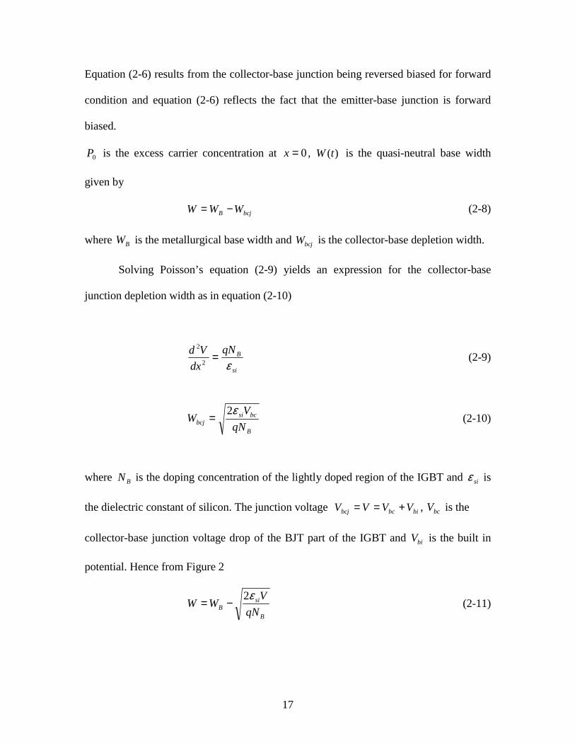
0P is the excess carrier concentration at 0=x , )(tW is the quasi-neutral base width
given by
bcjB WWW −= (2-8)
where BW is the metallurgical base width and bcjW is the collector-base depletion width.
Solving Poisson’s equation (2-9) yields an expression for the collector-base
junction depletion width as in equation (2-10)
si
BqN
dx
Vd
ε=
2
2
(2-9)
B
bcsibcj qN
VW
ε2= (2-10)
where BN is the doping concentration of the lightly doped region of the IGBT and siε is
the dielectric constant of silicon. The junction voltage bibcbcj VVVV +== , bcV is the
collector-base junction voltage drop of the BJT part of the IGBT and biV is the built in
potential. Hence from Figure 2
B
siB qN
VWW
ε2−= (2-11)

18
where ACEbc VVVV === is the collector-base voltage that appears across the drift
region.
2.3.2 Transient Operation of IGBT
While the turn-on time of the IGBT is quite fast, the turn-OFF time can be slow
because of the open base of the PNP transistor during the turn-OFF period. Figure 4
shows the typical IGBT turn-OFF transient where )0( −TI is the on-state current before
the initial rapid fall and )0( +TI is the current after the initial rapid fall. The initial rapid
drop in the anode current is due to the sudden removal of the MOS channel. This is
followed by a slower decay due to the removal of the carriers stored in the lightly doped
layer ( −n ). The turn-OFF process is initiated when we lower the gate voltage to a value
lower than the threshold voltage ( TV ) (first phase). This removes the formed electron
channel from under the gate and blocks the MOS component of the current MOSI .
0)( == WII nMOS in this case and the collector-base voltage bcV increases resulting in a
widening of the depletion region at the −n (base-collector side or source of MOSFET).
The relation between )0( −TI and )0( +
TI is through trβ [2]. It is the ratio of the
current immediately after the initial rapid fall to the magnitude of the fall and is shown
along with the ratio of )(tW to L ( )LtW )( in the appendices.
The switching losses of the IGBT are dominated by the losses, which occur
during the much slower second phase of the turn-OFF period transient. This is because of
the time required removing or extracting the injected carriers in this phase. This is a

19
major disadvantage of the IGBT device as it suffers from high-switching losses. This can
be overcome by reducing the lifetime of the carriers in the base through recombination or
extraction processes as quickly as possible before the device reaches its blocking voltage
state.
The collector-base junction is reversed biased and its depletion region widens
during the turn-OFF of the IGBT. When the IGBT is on, the status of the base-collector
junction is reversed biased as can be seen from Figure 2. When the IGBT is OFF, the
status of the base-collector junction is reversed biased and bcV is increased leading to
the increment of the depletion region since the current decreases. The widened region
supports the entire voltage drop across the device as mentioned previously based on
Poisson’s equation.
Since the quasi-neutral base width of the IGBT changes with time and decreases
with the increase of bcV , we can find an expression for the rate of rise of the voltage
across the device dt
tdV )( (varying of the output voltage) during the switching-OFF of the
IGBT from the collector-base junction depletion width bcjW expression as shown.
From B
bcsibcj qN
tVtW
)(2)(
ε= and the fact that )()( tWWtW bcjB −= if we take the time
derivative of )(tWbcj , we get
dt
tdV
tVqNdt
tdW
B
sibcj )(
)(2
)( ε=
20
and dt
dW
dt
tdW bcj−=)(=
dt
tdV
tVqNB
si )(
)(2
ε− (2-12)
This equation shows the time rate of change of the quasi-neutral base width ( )(tW ) that
covers almost all the length across the drift region during the turn-OFF since the
collector-base junction is reversed biased.
)0( −TI
)0( +TI
0=t t
Time
Ano
de C
urre
nt(A
)
)(tI
1
2
0Q
0FQα
Figure 4 Typical IGBT turn-OFF transient showing turn-OFF phases (1 and 2).
21
3.0 LITERATURE REVIEW ANALYSIS OF SOME
TRANSIENT MODELING OF IGBT
In Hefner et al. [3] transient modeling approach, the general ambipolar transport
electron current expression (t
xnqAD
b
tItWI T
n ∂∂+
+
= )(1
1
)())(( ) was used to find an
expression for the voltage rise (dt
tdV )(). MOSn ItWI =))(( as shown in Figure 3 and it is
important since it controls the operation of IGBT. Since the reverse bias on junction 2J
in Figure 1 does not increase rapidly and the depletion capacitance of junction 2J is
partially charged in a short period of time, MOSI current is instantaneous. An expression
for MOSI can be obtained if we consider the collector-base junction depletion capacitance
as in Figure 5. For the voltage )(tV between the plates, the charge per unit area
d
tVq si )(ε
= , where d is the distance between the plates and the rate of q change is
)(currentIdt
dq =
Q )()()( tVtCtq bcj=
dt
tdVtC
dt
tdCtV
tVtCdt
d
dt
dq
bcjbcj
bcj
)()(
)()(
))()((
+=
=∴

22
and in terms of the junction capacitance of the reverse biased junction, the displacement
current ))(( tWI n is
dt
tdVtC
dt
tdCtVWI bcj
bcjn
)()(
)()()( += . (3-1)
+ -
-----
+++++
C
V
d
I
Figure 5 The collector-base depletion capacitance formation.

23
The first term on the right hand side of equation (3-1) was ignored by Hefner. The rate of
change of )(tCbcj should be included in calculating the displacement current since the
capacitance varies with time as the depletion width changes with voltage [25]. From
equation (2-3) and the fact that A
IJ = , where A is the device active area
x
xpAqDtI
b
btWI Tn ∂
∂++
= )()(
1))((
and from Hefner’s approach
)(
)(1
1
2
11
)()()())((
tWx
pTbcjn x
xp
b
qAD
b
tI
dt
tdVtCtWI
=∂∂
++
+==
)(
)(2)(
)()()
11(
tWxpTbcj x
xpqADtI
dt
tdVtC
b =∂∂+=+ (3-2)
Hefner used equation (3-2) to obtain )(tV for the transient operation of IGBT. He
implemented the concept of moving the redistribution current. In his transient approach,
he neither used the steady state expression for )(xp (shown later) nor did he linearize the
steady state expression for )(xp .
His )(xp expression consists of two parts
dt
tdW
tW
xxtWx
DtW
P
tW
xPxp
)(
)(36
)(
2)()(1)(
320
0
−−−
−= (3-3)
From equations (2-3) and (3-3)
24
)(
)(
1
)())((
tWx
Tn x
xpqAD
b
tbItWI
=∂∂+
+=
)(
)(1
1
2
11
)())((
tWx
pTn x
xp
b
qAD
b
tItWI
=∂∂
++
+= (3-4)
and instead of equation (3-1), Hefner applied dt
tdVtCtWI bcjn
)()())(( = in his approach.
Integrating equation (3-3) in the base and multiplying by qA , the total charge Q
02
)(
)(
12
)(
12
)(
6
)(
)()
2
)()((
)(
)(1212
)(
6)()(2
)(
00
3330
0
)(
0
4230
2
0
×−=
−−−
−=
−−−
−=
= ∫
WD
qAPtWqAP
dt
tdWtWtWtW
DtW
PtWtWPqA
dt
tdW
tW
xxtWx
DtW
P
tW
xxqA
dxxpqAQ
tW
W
2
)(0 tWqAPQ = (3-5)
as can be seen dt
tdW )( has no effect on Q calculation.
We can find )(
)(
tWxdx
xp
=
∂ from equation (3-3) as
)(
200
)(
)(
)(3
3
6
)(
2
2
)()(
)(
tWxtWx dt
tdW
tW
xtWx
DtW
P
tW
P
x
xp
==
−−−=
∂∂
dt
tdWtW
tWtW
DtW
P
tW
P
x
xp )()(
6
)()(
)()(
)( 00
−−−
−=
∂∂

25
dt
tdW
D
P
tW
P
x
xp )(
6)(
)( 00 +−
=∂
∂
The hole current is x
xpqA
∂∂− )(
[3] and from the above equation
dt
tdWqAP
tW
qADP
dt
tdW
D
qADP
W
qADP
x
xpqAD
)(
6)(
)(
6
)(
00
00
−=
−=∂
∂−
2
)( 0PtqAWQ =Q
dt
tdW
tW
Q
tW
QD
x
xpqAD
)(
)(3)(
2)(2
−=∂
∂−∴ (3-6)
The first term on the right hand side of equation (3-6) is categorized by Hefner as the
charge control component and the second term is categorizes as the moving boundary
redistribution component of the hole current.
From equations (3-4) and (3-6)
dt
tdW
tW
Q
tWb
QD
b
tI
dt
tdVCtWI pT
n
)(
)(3
2
)(1
1
4
11
)()())((
2
−
+
−+
== .
This equation can be expressed in a different way if x
xpqAD
∂∂− )(
in equation (3-6) is
modified as
dt
tdW
tW
Q
tW
QD
x
xp
b
qAD
x
xpqAD p )(
)(3)(
2)(1
1
2)(2
−=∂
∂
+
−=
∂∂−
dt
tdW
btW
Q
btW
QD
x
xpqADp
)(11
)(3
11
)(
2)(2
2
+−
+=
∂∂−
( ) dt
tdW
btW
Q
bDDtW
QDD
x
xpqAD
np
npp
)(11
)(3
11
)(
4)(2
2
+−
+
+=
∂∂−
26
dt
tdW
btW
Q
tW
QD
x
xpqAD p
p
)(11
)(3)(
4)(2
2
+−=
∂∂− . (3-7)
From equation (3-4), we have
)(
)(1
1
2
11
)()())((
tWx
pTn x
xp
b
qAD
b
tI
dt
tdVCtWI
=∂∂
++
+==
this can be rearranged as
)(
)(2)(
)()(
11
tWxpT x
xpqADtI
dt
tdVtC
b =∂∂+=
+ .
Now using equation (3-7), and the fact that
)(2
2
)()()(
tV
NA
tW
AtCtC Bsi
bcj
sibcj
εε=== and
dt
tdV
qAN
C
dt
tdW
B
)()( −= ,
the above equation yields
dt
tdW
btW
tQ
tW
tQDtI
dt
tdVtC
bp
Tbcj
)(11
)(3
)(
)(
)(4)(
)()(
11
2
+−−=
+
+
−=
+
b
tW
tQDtI
NtqAW
tQ
dt
tdVtC
pT
Bbcj 1
1
)(
)(4)(
)(3
)(1
)()(
2
+
+
−
=
)(3
)(1
11)(
)()(
4)(
)( 2
tAWqN
tQ
btC
tQtW
DtI
dt
tdV
Bbcj
pT
(3-8)
where )0()( −≈ TT ItI for large inductive loads and )()(
4)(
2tQ
tW
DtI p
T = [Appendix A]
for the constant anode voltage in which 0)( =
dt
tdV indicating that the voltage and )(tW

27
are constants. Equation (3-8) is Hefner’s transient dt
tdV )( model for IGBT and )(tQ is
expressed by solving the following non-linear Hefner differential equation
2222
2
)(
)(4)()(
i
sne
HL nqAtW
ItQtQ
dt
tdQ −−≈τ
(3-9)
where sneI is the emitter electron saturation current (A) and in is the intrinsic carrier
concentration ( 3−cm ).
In Hefner’s approach, the negative of the collected hole current ))(( tWI p consists
of a charge control current ( CCI ) and redistribution current ( RI ), which make this model
more complex. The Expression2222
2
)(
)(4)()(
i
sne
HL nqAtW
ItQtQ
dt
tdQ −−≈τ
is not simple and 0Q
cannot be easily determined since there is no expression for 0P which can be substituted
for in 0Q equation to evaluate 0Q magnitude. Also, this model did not consider the rate
of change of )(tC in the calculation of the displacement current )).(( tWI n
Trivedi et al. [4] applied the steady state carrier distribution equation
()(
])([)( 0 LWnhsi
LxWnhsiPxp
−= ) for analyzing the turn-OFF process in the IGBT to derive
the dt
tdV )( expression. The net current following into the collector of the IGBT is
pnp
hhpnphTC
IIIII
αβ
−=+==
1 (3-10)
where =hI BJT base current similar to )(WIn in equation (3-2), =hpnp Iβ BJT collector
current similar to )(WI p in Hefner’s approach and
=
L
Wchsepnpα [1].

28
From equation (3-10), dt
tdWxqpxxqpI h
)()()()( == υ and
dt
tdW )( expression,
dt
tdV )(
was obtained as
−
−
−
= HL
t
si
B
T
Tp
etVqN
L
xWnhLsiI
tIL
Wchse
L
WshcoD
dt
tdV τ
ε)(2
)0(
)(12)(
(3-11)
−
HL
t
e τ was added to take care of the decay of charges due to the recombination in the
drift region. Trivedi et al. [4] multiplied HLτ in the exponent term by a constant κ to
account for the effect of both carrier recombination and electron current injection sneI .
This approach of multiplying κ with HLτ alters the real value of HLτ . The modeling
approach for the dt
tdV )( in [4] is different from Hefner’s approach due to different key
assumptions and equations used for the ambipolar electron and hole currents to analyze
the turn-OFF process in the IGBT. This model ignored the diffusion effects of the carriers
in the quasi-neutral base in the IGBT analysis besides using a positive expression for
dt
tdW )( which should be negative since ( )()( tWWtW bcjB −= ).
Ramamurthy et al. [5] used different coordinate systems for modeling the
transient turn-OFF of IGBT as shown in Figure 6 (i.e. xW = and 1dWB = ). The steady
state carrier distribution equation ()(
])([)( 0 LWnhsi
LxWnhsiPxp
−= ) was applied to find 0P
expression.

29
0P was calculated from the total diffusion current density TJ with the use of
boundary conditions for electron currents nJ , the hole current pJ and the total current
TJ as
pp JWxJ === )0( (3-12)
)0()0()0( ==−===== WxJWxJWxJ pTn (3-13)
)0()0()0( ==+===== WxJWxJWxJ pnT . (3-14)
From equations (3-12) to (3-13) and the expression for x
xpqD
b
JJ T
n ∂∂+
+
= )(1
1, 0P is
expressed as
p
n
pT
n
pp
qD
JJL
WnhLta
P2
1)0(
0
−
+
=µµ
µµ
.
Substituting for
−==
BW
xPWxP 1)( 0 as in [5], one gets
p
Bn
pT
n
pp
qD
W
WJJ
L
WnhtaL
Wp2
11)0(
)(
−
−
+
=µµ
µµ
. (3-15)
The sweeping-out action of charges was applied to find dt
tdV )( the turn-OFF analysis
dt
tdWxqApIT
)()(= (3-16)
)()( tWWtW bcjB −=Q
and B
sibcj qN
tVtW
)(2)(
ε=

30
dt
tdV
tVqNdt
tdW
B
si )(
)(2
)( ε−=∴ .
From equations (3-15), (3-16) and
−==
BW
xPWxP 1)( 0
dt
tdV
tVqNxqApI
B
siT
)(
)(2)(
ε−=
si
B
B
T tVqN
W
WqAP
I
dt
tdV
ε)(2
1
)(
0
−
−=
00
1)(
P
dNJ
AP
WNI
dt
tdV
si
BT
si
BBT
εε−
=−
= (3-17)
Ramamurthy et al. [5] used a positive value for dt
tdW )( instead of a negative value
which contradicts the equality )()( tWWtW bcjB −= .
31
0=W 1dWB =W
bcjW
EmitterE
BaseB
CollectorC
Dep
letio
n re
gion
Figure 6 Adjusted coordinate system used for Ramamurthy analysis [5].

32
4.0 A NEW PHYSICS-BASED TRANSIENT MODEL
4.1 The Steady State
As mentioned in section 2.3.1, the steady state expression for )(xp can be
obtained by solving the ambipolar diffusion equation in the base ( 0)()(
22
2
=−∂
∂L
xp
x
xp)
under the boundary conditions [2]
0)( == Wxp (2-6) 0)0( Pxp == . (2-7) This equation has the solution of the form
( ) ( )LxLx
BeAexp −+=)(
Solving for the constants A and B , )(xp is expressed as
( )[ ]
( )LWnhsi
LxWnhsiPxp
−= 0)( . (4-1)
Integrating equation (4-1) and multiplying by qA , the total charge stored 0Q in
the base is obtained as
== ∫ dxxpqAPQW
000 )(( )
( )
−LWnhsi
LWshcoqAP
10
Using the identities ( ) ( )xx 2sinh212cosh += and ( ) ( ) ( )xxx coshsinh22sinh = leads to
33
( )LWnhtaqALPQ 200 = (4-2)
this 0Q results from on-state transient.
0P which results from the turn-on state, can be calculated by using the general
ambipolar transport hole current, the steady state excess carrier distribution equation (4-
1), and the following boundary conditions for electron, hole and the total currents
0)0( ==xI n (4-3)
Tp IxI == )0( (4-4)
pnT III +=Q
pT II =∴ .
The assumption of 0)0( =nI is valid for electron carriers in the turn-on state because the
quasi-neutral base width ( BbcjB WWWW ≈−= since 5.2≈CEV volts) equals the
metallurgical base width ( BW ). As a result, electrons do not have sufficient time to reach
the emitter side of BJT part of IGBT to recombine with the injected hole carriers and
constitute electron current.
Using equations (2-4) and (4-1), an expression for 0P is
( )LWnhtaqAD
LIP
p
T
2
)0(0
−
= (4-5)
where )0( −TI is the steady state turn-on current, which is used as the initial current at
the start of turn-OFF period.
Solving equations (4-2) and (4-5), 0Q can alternatively be expressed as
34
( )[ ]LWchseD
ILQ
p
T −=−
12
)0(2
0 . (4-6)
This is the steady state turn-on charge and W is constant in association with 0Q .
For a given )0( −TI , ( HLQ τ−0 ) curves can be produced as shown in Figure 7
for different )0( −TI values. As can be seen, 0Q is proportional to )0( −
TI and dependent
on HLτ through HLDL τ=2 that stems from the term ( ) ( )HLDWchseLWchse τ= . We
can also notice that the voltage V in (B
siB qN
VWW
ε2−= ) term corresponds to the steady
state voltage across the BJT, which amounts to a value of approximately 2.5 volts.
4.2 Turn-OFF Transient
During the turn-OFF of the IGBT the excess carrier base charge, which was built
up during the turn-on, will decay by recombination in the base and by electron current
injection into the emitter:
)0()()(
nHL
ItQ
dt
tdQ −−=τ
.
Assume 0)0( =nI
The assumption of 0)0( =nI is valid for electron carriers in turn-OFF transient (gate
voltage TV⟨ ) because the sudden removal of the MOS channel will prevent the
attraction of electrons from the +p body directly under the gate. As a result, no electron
carriers will be available to reach near the emitter part side of BJT part of IGBT to

35
recombine with the injected hole carriers and constitute electron current.
HL
tQ
dt
tdQ
τ)()( −=∴
this has the solution of the form
−
′= HL
t
eQtQ τ0)( (4-7)
where 0Q′ = 0FQα and 0Q was obtained from the steady state analysis where
( )[ ]( )LWnhsi
LxWnhsiPxp
−= 0)( which is used as an initial condition for the transient analysis.
W is almost constant in association with 0Q . As can be seen from Figure 4 region 1, a
sudden drop in current from )0( −TI to )0( +
TI will change the magnitude of 0Q
associated with )0( −TI to a lower value 0Q′ = 0FQα associated with )0( +I and F should
be less than 1.0. In region 2 where there is a slow decay of current, equation (4-7) applies
because that is where recombination takes place.
4.2.1 Expression For dt
tdVCE )(
In the turn-OFF period for NPT IGBT since there are no recombination centers,
the ambipolar diffusion length is larger than the drift layer which implies )(tWL ⟩⟩ and
)(tWWB ⟩⟩ . This is true as carrier lifetimes increase. This is shown if we calculate
HLDL τ= for different lifetimes and assume 400)( == BUSVtV volts.

36
For SHL µτ 3.0= , cmL 3103.2 −×= , cmL 3106.6 −×= for SHL µτ 45.2= and
cmL 21013.1 −×= for SHL µτ 1.7= . Since cmW 3102.4 −×= , )(tWL ⟩⟩ as carrier
lifetimes increase.
The hole distribution is not the same as given by equation (4-1). It can however be
estimated by expanding equation (4-1) using Taylor series to yield a first order
approximation as
( )[ ]
( )LtWnhsi
LxtWnhsitPtxp
)(
)()(),( 0
−=
( )[ ] ( )
( ) .....)()(
)(
.....)()(
)(
3
3
3
3
++=
+−+−=−
L
tW
L
tWLtWnhsi
L
xtW
L
xtWLxtWnhsi
( )
−=
−
=)(
1)()(
)()(
),( 0
0
tW
xtP
L
tWL
xtWtP
txp
−=
)(1)(),( 0 tW
xtPtxp . (4-8)
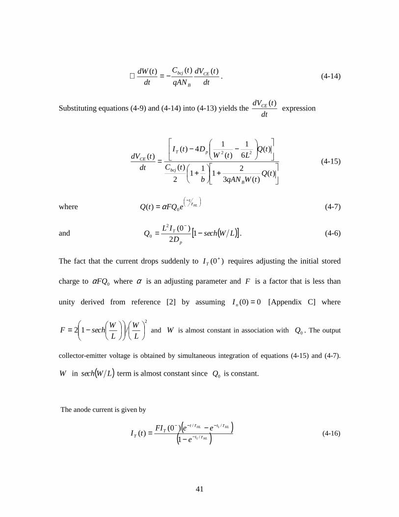
Equation (4-8) is plotted for )(xp as in Figure 8 which shows a linear carrier profile at a
given time t . From this Figure the slope (dt
tdW
tW
P
t
P )(
)(00 −
=∂
∂) is negative since the
behavior of )(tW tends towards the minus x -direction as the device voltage )(tV
changes with time (moving boundary) [Appendix A].
37
By integrating equation (4-8) through the base and multiplying by qA , the total
charge )(tQ is found as
)(2
)(),()()( 0
0
0 tPtqAW
dxtxptqAPtQW
== ∫ .
Using the above equation, the carrier concentration at the emitter edge of the base )(0 tP
is related to )(tQ as
)(
)(2)(0 tqAW
tQtP = (4-9)
The accuracy of the voltage waveform in transient is highly correlated to ),( txp .
Hence additional improvement on the hole carrier profile is required by substituting
equation (4-8) into time dependent diffusion equation (t
txp
DL
txp
x
txp
∂∂+=
∂∂ ),(1),(),(
22
2
),
by integrating twice with respect to x , by using the boundary condition
)(),0( 0 tPtxp == , 0),( == tWxp as well as using the following relation [Appendix A]
dt
tdW
tW
tP
t
tP )(
)(
)()( 00 −=∂
∂
we get 1
2
20 ),(1
)(2
)(),(C
t
txp
DtW
xx
L
tP
x
txp +∂
∂+
−=
∂∂
∫ .
t
txp
∂∂ ),(
comes from equation (4-8) as
dt
tdW
tW
xtP
tW
x
t
tP
t
txp )(
)(
)(
)(1
)(),(2
00 +
−
∂∂
=∂
∂.
Substituting the above equation in the previous integral yields

38
10
2
20
2
20 )(
)(
)()(
)(
)(1
)(2
)(),(C
dt
tdW
tW
xtP
dt
tdW
tW
xtP
DtW
xx
L
tP
x
txp +
−+
−=
∂∂
(4-10)
Now integrating equation (4-10) with its constant 1C once with respect to x , we get
21
20
2
30
32
20
)(2
)(
)(3
)()(1
)(62
)(),( CxC
tW
xtP
tW
xtP
dt
tdW
DtW
xx
L
tPtxp ++
−+
−=
Using the following boundary condition ( )(),0( 0 tPtxp == , 0),( == tWxp , we get )(02 tPC =
dt
tdW
D
tP
L
tPtW
tW
tPC
)()(
6
1
3
)()(
)(
)( 0300
1 +−−
=
)()()(
6
1
3
)()(
)(
)(
)(2
)(
)(3
)()(1
)(62
)(),(
00
200
20
2
30
32
20
tPdt
tdW
D
xtP
xtW
L
tP
tW
xtP
tW
xtP
tW
xtP
dt
tdW
DtW
xx
L
tPtxp
++
−−
−+
−=∴
dt
tdW
D
xtP
tW
xtP
tW
xtP
dt
tdW
DtP
L
xtWtP
tW
xtP
tW
xx
L
tPtxp
)()(
6
1
)(2
)(
)(3
)()(1)(
3
)()(
)(
)(
)(62
)(),(
0
20
2
30
0200
32
20
+
−++−−
−=
( )
+−+
+−−−=
6
)(
2)(3
)(
)(
)(1
3
)(
)()62)(),(
230
22
3
2
2
0
txWx
tW
x
dt
tdW
DtW
tP
L
txW
tW
x
LtW
x
L
xtPtxp
+−+
+−−−=
6
)(
2)(3
)()(
)(
11
3
)(
)()(62)(),(
23
022
3
2
2
0
txWx
tW
x
dt
tdWtP
DtWL
txW
tW
x
LtW
x
L
xtPtxp

39
+−+
−−+−=
6
)(
2)(3
)()(
)(
1
3
)(
)(62)(1)(),(
230
22
3
2
2
0
txWx
tW
x
D
tP
dt
tdW
tWL
txW
LtW
x
L
x
tW
xtPtxp
The refined version for the hole distribution during transient is therefore expressed as
−−−
−−+−=
)(36
)(
2
)()(
)(
1
3
)(
)(62)(1)(),(
320
22
3
2
2
0 tW
xxtWx
D
tP
dt
tdW
tWL
txW
LtW
x
L
x
tW
xtPtxp
(4-11)
Integrating equation (4-11) and multiplying by qA yields the charge )(tQ
−=
2
3
0 24
)(
2
)()()(
L
tWtWtqAPtQ
Since )(tWL ⟩⟩ , the second term can be neglected leading to the previous equation (4-9)
)(
)(2)(0 tqAW
tQtP = . (4-9)
Substituting for )(0 tP in equation (4-11) leads to ),( txp as function of )](),(,[ tWtQx .
Equation (4-11) is similar to Hefner’s )(xp expression et al. [2] except for three
additional terms which modify the linear dependence of p on x .
Since )(tWL ⟩⟩ , we substitute for )(0 tP in equation (4-11) by its value
from equation (4-9) to calculate dt
txp ),(∂ expression in the equation of the displacement
current )(WIn . The base current ( )nI W is a displacement current in nature and results from
the discharge of the reverse-biased collector-base depletion junction capacitance )(tCbcj
dt
tdVtC
dt
tdCtVWI
tVtCdt
dWI
CEbcj
bcjCEn
CEbcjn
)()(
)()()(
))()(()(
+=
=
40
where )(2)(
)(tV
NqA
tW
AtC
CE
bsi
bcj
sibcj
εε== .
Since )()( tWWtW bcjB −=
then dt
tdV
qAN
tC
dt
tdW CE
B
bcj )()()( −=
and the displacement current is
dt
tdVtCWI CEbcj
n
)(
2
)()( = . (4-12)
This type of current flow is usually called the displacement current. The rate of change of
)(tCbcj must be included when calculating this current, since the capacitance varies with
time as the depletion width change with voltage.
Using equation (4-11), (4-12) and the displacement current equation
)(
),(1
1
)()(
tWx
Tn x
txpqAD
b
tIWI
=∂∂+
+=
, )(
),(
tWxx
txpqAD
=∂∂
is expressed as
dt
tdW
D
tqAP
tWL
tWtqADP
x
txpqAD
tWx
)(
6
)(
)(
1
6
)()(
),( 020
)(
+
−=
∂∂
=
dt
tdWtqAP
tWL
tWtqADP
b
tI
dt
tdVtCWI Tbcj
n
)(
6
)(
)(
1
6
)()(
11
)()(
2
)()( 0
20 +
−+
+
==∴ (4-13)
)()( tWWtW bcjB −=Q and B
sibcj qN
tVtW
)(2)(
ε=
and )(2)(
)(tV
NqA
tW
AtC bsi
bcj
sibcj
εε==Q
41
dt
tdV
qAN
tC
dt
tdW CE
B
bcj )()()( −=∴ . (4-14)
Substituting equations (4-9) and (4-14) into (4-13) yields the dt
tdVCE )( expression
+
+
−−
=)(
)(3
21
11
2
)(
)(6
1
)(
14)(
)(22
tQtWqANb
tC
tQLtW
DtI
dt
tdV
B
bcj
pT
CE (4-15)
where
−
= HL
t
eFQtQ τα 0)( (4-7)
and ( )[ ]LWchseD
ILQ
p
T −=−
12
)0(2
0 . (4-6)
The fact that the current drops suddenly to )0( +TI requires adjusting the initial stored
charge to 0FQα where α is an adjusting parameter and F is a factor that is less than
unity derived from reference [2] by assuming 0)0( =nI [Appendix C] where
2
/12
−=
L
W
L
WchseF and W is almost constant in association with 0Q . The output
collector-emitter voltage is obtained by simultaneous integration of equations (4-15) and (4-7).
W in ( )LWchse term is almost constant since 0Q is constant.
The anode current is given by
( )
( )HL
HLHL
t
ttT
Te
eeFItI τ
ττ
/
//
1
1
1
)0()( −
−−−
−−
= (4-16)

42
and 1t corresponds to the time t when the output voltage )(tVCE reaches the supply bus
voltage.
The above equation applies to the slow decay of current because it is there where
recombination takes place while the total current in the ambipolar transport current
equation (t
txpqAD
b
tIWI T
n ∂∂+
+= ),(
)1
1(
)()( ) relates the hole current to the displacement
current when calculating the anode voltage expression.
It is instructive to note that by multiplying )(tQ by the correction factor Fα , the
extracted charges in the base are reduced by this factor. The displacement current
dt
tdVtC CE
bcj
)()( should therefore be also reduced by the same factor Fα for scaling purpose in
order to account for the reduced charge in the base during the turn-OFF transient.
This new physics-based model has several advantages over Hefner’s model:
. The non-linear capacitance is included in the calculation of the displacement current.
This is unlike Hefner’s model where the capacitance was assumed constant.
. The ambipolar diffusion equation (time-dependent) is totally implemented without
neglecting the first part on the right hand side (2
)(
L
xp) of that equation. However, Hefner
et al. [2] did not take this point into account.
. The initial steady state base charge 0Q for each HLτ can be computed easily in any
commercial software programs since the expression for dt
tdQ )( is simpler than Hefner’s
dt
tdQ )( expression. In the new model, 0P is not used as an adjusting parameter.

43
However, in Hefner’s model, the initial steady state base charge 0Q magnitude at
different HLτ must be provided separately in the software program since dt
tdQ )(
expression is non-linear and has more than one dependent variable ( HLτ , )(tW ).
. The expression for 0P is simple and computable due to the boundary conditions.
However, 0P was used as a parameter in Hefner’s model and does not have a simple
expression.
. The model is not a complex function of the redistribution current ( RI ), which is due to
the redistribution component of the carrier distribution.
Figure 9 compares the output voltage waveforms for different carrier lifetimes for
this model with measured (experimental) data outputs and model in [2] for large
inductive loads (10A). Theoretical predictions of the output voltages have been obtained
with different carrier lifetimes and compared with experimental data available in the
literature and good agreement has been obtained.

44
Figure 7 The steady state charge 0Q as a function of the load current and
carrier lifetime HLτ .
45
Figure 8 Linear excess carrier concentration profile as a function of
distance )(tW .
46
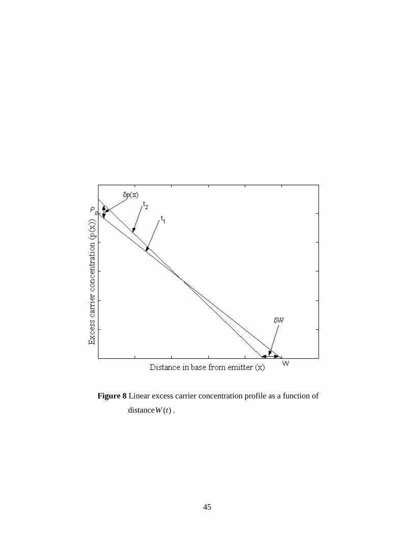
Figure 9 Comparison of anode voltages with the experimental data for different
lifetimes.

47
GVBUSV
+
+
Pulse
PNP IGBT= 400 V
+10 V-10 V
R L(Large)
Figure 10 Large inductive loads with no freewheeling diode in an IGBT turn-OFF circuit.
48
GVBUSV
+
+
Pulse
PNP IGBT= 400 V
+10 V-10 V
R L(Large)
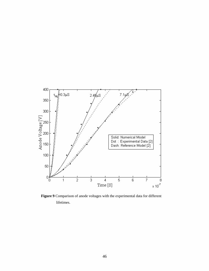
Diode
Figure 11 Inductive loads with a freewheeling diode in an IGBT turn-OFF circuit.

49
Table 1 IGBT Model Parameters
MODEL PARAMETERS
VALUES
UNITS
BW m3.9 cm
A 0.1 2cm
BN 14102 × 3−cm
HLτ SHL µτ 3.0= -> 1310 (n/ 2cm )
SHL µτ 45.2= > 1210 (n/ 2cm )
SHL µτ 1.7= > -- (n/ 2cm )
Sµ
( )b
D
DD
DDD p
pn
pn
11
22
+=
+=
18 cm
L Varies ( HLτ dependent) cm
50
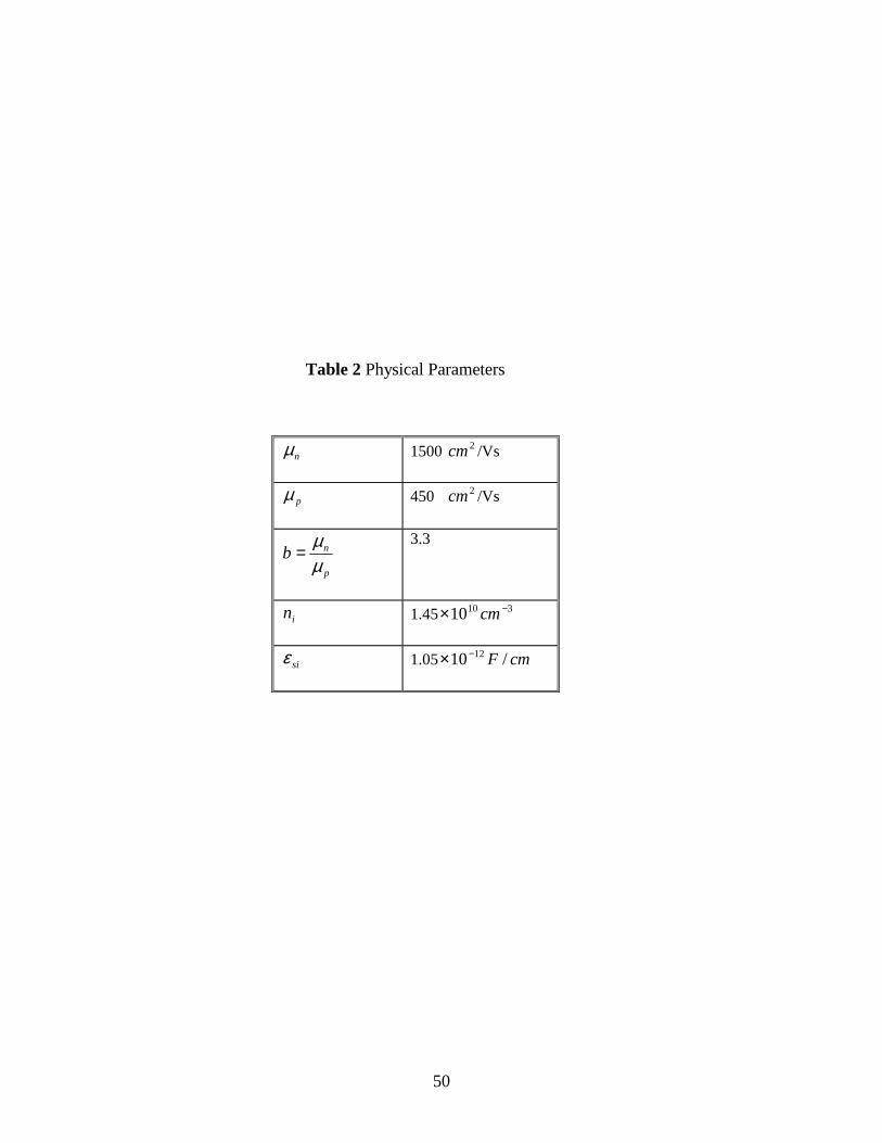
Table 2 Physical Parameters
nµ 1500 2cm /Vs
pµ 450 2cm /Vs
p
nbµµ
= 3.3
in 1.45 31010 −× cm
siε 1.05 cmF /10 12−×
51
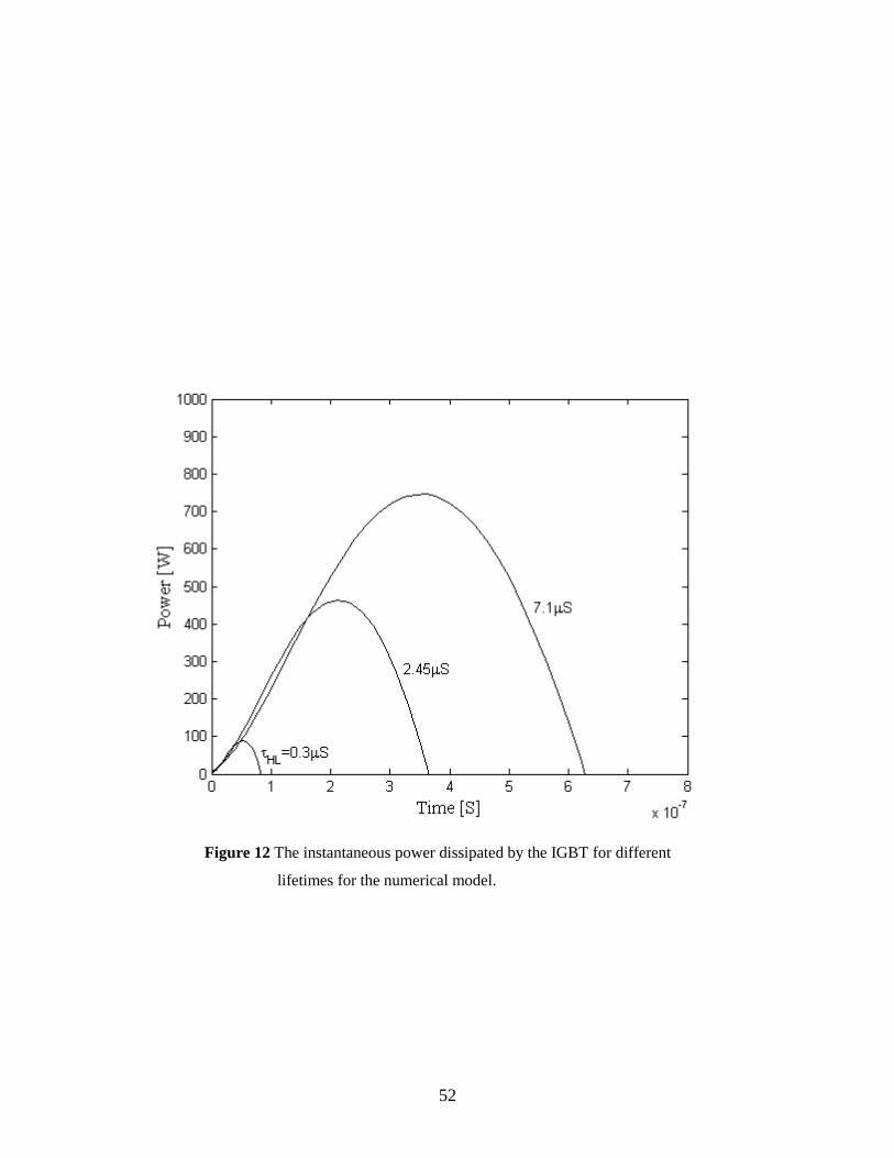
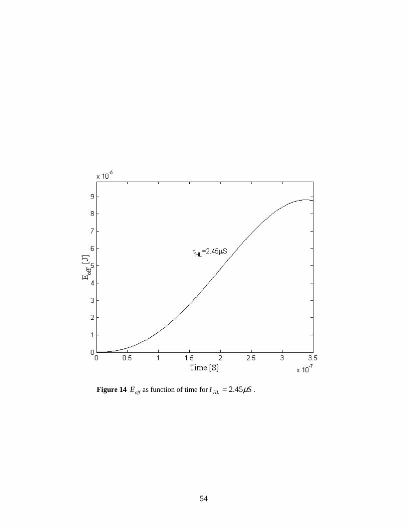
4.2.2 The Instantaneous Power )(tP and Switching Losses )(tEoff :
Transient losses occur when switching action takes place in an IGBT. Since the
IGBT sustains high anode current density and voltage simultaneously, high power
dissipation occurs. The instantaneous power )(tP dissipated by the IGBT is the product
of the voltage and the anode current ( )(*)( tItV TCE ). From voltage equation (4-15) and
current equation (4-16), different power profiles for different device lifetimes HLτ are
produced as shown in Figure 12. At higher lifetimes, because of a larger number of
carriers, the current is high and as a result the corresponding power dissipation is larger.
The transient turn-OFF energy offE results from integrating the instantaneous power
over a time interval. For a given value of the device anode current, one data energy point
is calculated. The energy results for different device lifetimes are shown in Figures 13,
14 and 15 separately. The comparison of theses energy level losses is shown in Figure 16.
To produce offE as a function of the anode current, these energy points for particular
anode current values at different device lifetimes are plotted in Figure 17.
52
Figure 12 The instantaneous power dissipated by the IGBT for different
lifetimes for the numerical model.

53
Figure 13 offE as function of time for SHL µτ 3.0=
54
Figure 14 offE as function of time for SHL µτ 45.2= .

55
Figure 15 offE as function of time for SHL µτ 1.7= .

56
Figure 16 Comparison of the energy losses for three different lifetimes in
an IGBT for the numerical model.

57
Figure 17 Turn-OFF switching losses ( offE ) as a function of anode current
for the numerical model.

58
4.2.3 An Alternative Analytical Solution For The Transient dt
tdVCE )(:
An alternative analytical solution for the proposed transient turn-OFF of the NPT
IGBT is presented. The solution is derived by considering equation (4-15), by assuming an
initial solution and using one iteration to obtain a closed form expression for the transient voltage.
A constant β is used to adjust the steady state charge 0Q . Based on this approach, the depletion
width can be expressed as
taRWbcj max= (4-17)
where B
si
qNR
ε2=
and maxa is the slope of the initial voltage with time and differs from structures and carrier
lifetime.
From equation (4-15), the gradient of anode voltage with time is given as
+
+
−−
=)(
)(3
21
11
2
)(
)(6
1
)(
14)(
)(22
tQtWqANb
tC
tQLtW
DtI
dt
tdV
B
bcj
pT
CE (4-15)
For the turn-OFF transient, )(tWL ⟩⟩ for which )(
11
tWL<< then equation (4-15)
becomes
+
+
−
=)(
)(3
21
11
2
)(
)()(
4)(
)( 2
tQtWqANb
tC
tQtW
DtI
dt
tdV
B
bcj
pT
CE (4-18)
59
The above equation can be alternatively be simplified under the assumption that
1)(3
)(2 >>tWqAN
tQ
B
to read
+
−
=−
−
)(3
11)(
)(
4)(
)()/(
0
)/(02
tWqAN
eQ
btC
eQtW
DtI
dt
tdV
B
t
bcj
tpT
CE
HL
HL
τ
τ
β
β. (4-19)
By replacing max
)(a
dt
tdVCE = and using the following relations:
)()()(
3
)1
1(
)()(
tVRWtWWtW
RqANb
rR
Ar
tW
AtC
CEBbcjB
Br
si
bcj
sibcj
−=−=
+=
=
=
ε
ε
equation (4-19) becomes
)()(
)(
4
)()(
)()/(
0
)/(02
)/(0
max
tVtW
eQR
eQtW
D
tVtW
eQR
tIa
CE
tr
tp
CE
tr
T
HL
HL
HL τ
τ
τ β
β
β −
−
− −= .
Multiplying both sides of the above equation by ttVRWeQR CEBt
rHL ))(()/(
0 −− τβ ,
collecting terms and doing some algebraic manipulations [Appendix D]; the anode
voltage )(tVCE can be obtained as a function of time and charge )(tQ as
2
22
2
.4.2)(
A
CABBCABCE R
tRRRRtRRRtV
−−−= (4-20)
60
where
)4)((
).)(2(
).)((
)/(0
2
)/(0
)/(0
HL
HL
HL
tpTBC
trBB
trA
eQDtIWR
tRtIeQRWR
tRtIeQRRR
τ
τ
τ
β
β
β
−
−
−
−=
+=
+=
Equation (4-20) can be successfully applied to PT IGBT by adding extra terms in )(tQ
so that it covers all the IGBTs regardless of structures modified by any reason. In
equation (4-20), the value for 0Q is substituted from equation (4-5). The parameters used
for developing the above models are summarized in Tables 1 and 2
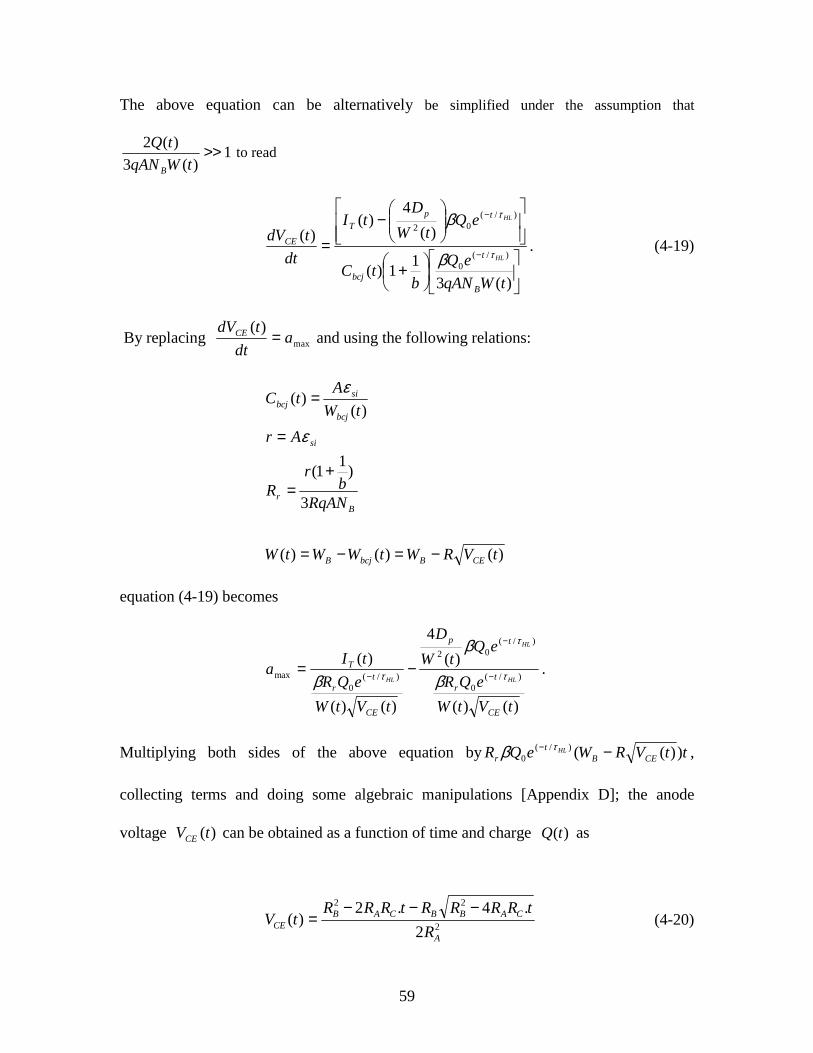
The outputs of the analytical model of equation (4-20) for different lifetimes are
shown in Figure18. The results are compared with the numerical model and the
experimental data [2]. Figure19 shows the anode current profile for SuSHL µτ 45.2,3.0=
and Sµ1.7 . The analytical model anode voltage is compared with the numerical one and
with the model in [2] in Figure 18 for =HLτ uS1 , uS4 and uS6 respectively.
Transient losses occur when switching action takes place in an IGBT. Since the
IGBT sustains high anode current density and voltage simultaneously, high power
dissipation occurs. The instantaneous power )(tP dissipated by the IGBT is the product
of the collector-emitter voltage and the anode current ( )()( tItV TCE × ). The anode current
is given by
( )
( )HL
HLHL
t
ttT
Te
eeFItI τ
ττ
/
//
1
1
1
)0()( −
−−−
−−
= (4-16)
61
Figure 18 Comparison of anode voltages with different lifetimes for the analytical
model and experimental data.

62
Figure 19 Anode current profiles.

63
Figure 20 Comparison of anode voltages with the reference model for different lifetimes.
64
Figure 21 maxa values for different lifetimes for NPT IGBT structure for
the analytical model.

65
5.0 RESULTS AND DISCUSSION
A new physics-based model for NPT IGBT for the transient turn-OFF was
developed in chapter 4. The instantaneous power dissipation and the switching energy
loss profiles have been produced. An alternative analytical solution for this model has
been generated beside a numerical solution.
The numerical anode output voltages are compared with the experimental data
and reference model [2] in Figure 9 for 3 different lifetimes SSHL µµτ 45.2,3.0= and
SHL µτ 1.7= as measured by Hefner for a device whose parameters are listed in Tables 1
and 2. The output results show good agreement over the wide range of lifetimes. In
reference [2], a large inductive load was used in the simulation with no freewheeling
diodes. The circuit used is shown in Figure 10. Since the current through an inductor can
not change instantaneously, it follows that in this case )(tIT appearing in equations (4-
15) and (4-20) is constant and equal to )0( −TI . It is instructive to note that the nature of
)(tIT in the model depends on the load condition in the circuit. If the load is purely
resistive, the current )(tIT can not be constant.
The device lifetime determines the output voltage behavior. The injected holes
from the emitter of the BJT part of the IGBT get recombined with the electrons coming
from the n channel of the MOSFET portion of the IGBT. The excess carrier lifetimes in
the base of the IGBT determine the amount of current available in the IGBT. For lower
carrier lifetimes, the current is lower as well and, as a result, the output anode voltage

66
builds up faster and reaches the supply bus voltage. On the other hand, as the carrier
lifetime increases, the amount of the produced current increases as well and the output
voltage is decreased as shown in Figure 9. The average error between the theoretical
predictions of numerical simulation compared with the experimental data for lower
carrier lifetimes is within 6% with the accuracy increasing for higher carrier lifetime. The
corresponding average error for the analytical model is within 4%. Typical carrier
lifetime range is from 1 to 2 Sµ for practical applications. The new models reveal good
agreement for this range. Commercial MATLAB software was used in developing
different output results [26].
The instantaneous power dissipation and the switching energy losses in the case
of free wheeling diode for different anode currents and lifetimes are shown in Figures 12
and 16. The circuit used is shown in Figure 11. The instantaneous output power is the
product of the anode voltage and anode current. The anode current expression (4-16) is
used in conjunction with the output voltage to produce the power and energy losses.
Figure 19 shows the anode current profiles for three different device lifetimes ( HLτ ) when
using a circuit that has a free wheeling diode in parallel with an inductor. In the turn-ON
of IGBT, a steady state current )0( −TI flows in the IGBT. At the turn-OFF switching,
this steady state current drops initially to a value of )0( −TFI then decays exponentially
due to the recombination in the base and should reach a zero value at a time 1tt = when
the collector-emitter voltage reaches the supply bus voltage. Carrier lifetime determines
the exponential decay rate with faster decay when carrier lifetime is smaller. Higher
carrier lifetime requires more time for extraction or removal when the device turns-OFF.
This power output depends upon the injected carrier lifetime with higher power

67
dissipation for higher carrier lifetime. From Figure 16, the switching energy losses are the
integral of the power output over the time interval. The switching energy losses can also be
displayed as function of the anode current TI as shown in Figure 17. For many
commercially available IGBT packages, data are provided for the switching losses as a
function of the anode current. The anode current for theses packages ranges from 500 A
to 2500 A. However, for lower ranges of anode currents, data are not readily available.
The current of Figure 19 has a different decay rate during the turn-OFF for different
carrier lifetimes. With lower carrier lifetime, the slope of current decay is very sharp
hence the stored base charge extraction is abrupt. As a result, the energy loss is low and
visa versa. This confirms the behavior of the switching of energy verses the device anode
current. From these results, the power dissipation and energy losses increase with the
increase of the carrier lifetime and anode current. The average error of different
comparisons is within 5%.
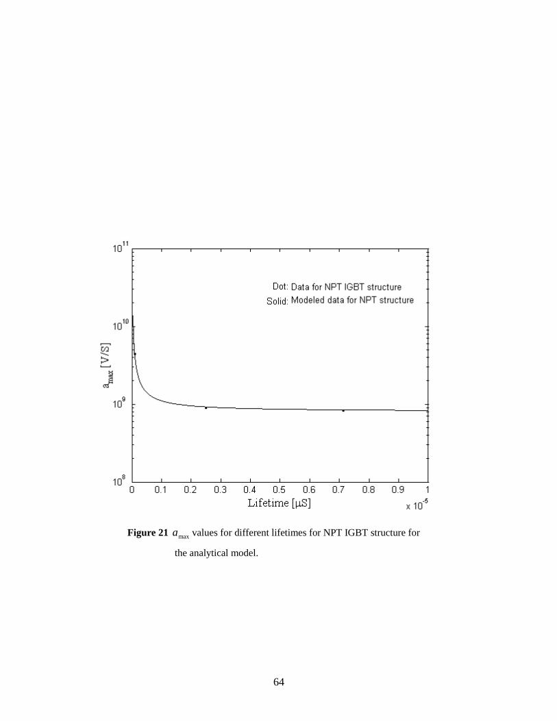
For the alternative analytical solution of the numerical model, the transient
behavior of maximum available gradient of voltage maxa is shown in Figure 21. The
transient charge )(tQ value is reduced from 0Q to 0Qβ . The depletion width in 0Q
expression comes from equation (4-5) and maxa is lifetime and structure dependent. A
value of 9.0=β was used to develop the I-V characteristics of the NPT IGBT.
Figure 18 shows an excellent agreement between the alternative analytical model
and the experimental data available in literature for the three lifetimes. This confirms the
validity of the assumptions made to develop the simple analytical model.
Figure 20 provides additional comparison between the analytical, numerical and
data obtained from substituting in the equations of reference [2] since experimental data

68
are not readily obtainable. The analytical model of [2] with the given parameters can be
used as a reference for the comparison since it is the most developed comprehensive
model in the literature. From this Figure, the average error for lower carrier lifetime
( SHL µτ 3.0= ) is within 5% with the accuracy increasing for higher carrier lifetime. The
outputs are, in general, in good agreement.

69
6.0 SUMMARY AND FUTURE WORK
This thesis dissertation dealt with the modeling and simulation of the Insulated
Gate Bipolar Transistors, which is a preferred power-switching device. A Physics-based
model for the NPT IGBT during the turn-OFF period was developed based on the
solution of a one-dimensional ambipolar diffusion equation which results from high
injection levels of minority hole carriers. The ambipolar transport equations are analyzed
in detail. This model was compared with Hefner’s model el al. [2] and found to be much
simpler and can be implemented easily in commercial software programs. The output
predictions are in good agreement with the available literature experimental data.
An analytical solution was introduced in addition to the numerical approach. This
approach has a very simple linear form that is easily solvable. The advantage of this
model is that it is suitable for and can be applied to different structures of an IGBT (PT
IGBT) by applying appropriate charge models.
Since the IGBT sustains high current and voltage simultaneously during the
switching-OFF transient, there is high power dissipation in the device. The turn-OFF
power dissipation and energy losses were introduced and simulated.
The output characteristics for both the collector-emitter voltage and the anode
current can be compared in time point by point and plotted. The interception of the DC
line from KCL in a circuit with the produced I-V characteristics will determine the
operating point.
The validity of the newly developed models was confirmed by comparison to the
available experimental data or the reference model [2].

70
A future topic of research would be to expand and apply the ideas used in these
models to new device structures and then implement them in SABER software simulation
to confirm the validity of the developed model compared to the experimental data
available in the literature.

APPENDICES

72
APPENDIX A
LINEAR CHARGE CONTROL
From the steady state analysis we have
( )[ ]
( )LWnhsi
LxWnhsiPxp
−= 0)( (A-1)
Since the diffusion length ( L ) is larger than the drift layer thickness ( BW ) because of the
high lifetime of carriers, one can approximate the carrier profile for the holes )(xp in the
drift layer by a linear expression as shown previously
−≈
)(1),( 0 tW
xPtxp . (A-2)
With the aid of the general ambipolar transport hole current expression
( ) x
xpqADtI
bI Tp ∂
∂−+
= )()(
1
1 (A-3)
we can find an expression for 0P from equations (A-2) and (A-3) as
)(
)( 0
tW
P
x
xp −=∂
∂ (A-4)
0)0( =nIQ
)()0( tII Tp =∴
and ( ) )(11
2
1
)()()0( 0
tW
P
b
qAD
b
tItII pT
Tp
+
++
==

73
( ) )(11
2
1
11)( 0
tW
P
b
qAD
btI p
T
+
=
+
−
)0()0()( −=== TT ItItI
p
T
qAD
ItWP
2
)0()(0
−
= . (A-5)
Since total anode current is constant ( )0()( −= TT ItI ), from the above equation we can
find t
P
∂∂ 0 as
dt
tdW
qAD
I
t
P
p
T )(
2
)0(0−
=∂
∂ .
Substituting for )0( −TI from equation (A-5), the above equation becomes
dt
tdW
tW
P
t
P )(
)(00 −
=∂
∂. (A-6)
From Figure 8 this slope is negative since the behavior of )(tW tends towards the minus
x -direction as the device voltage )(tVCE varies with time (moving boundary).
The total charge in the base of the IGBT is
−=
−=
−=
−= ∫
2
)()()(
2
)()()(
)(2)(1)(
0
2
0
0
2
0
0
0
tWtWqAPtQ
W
tWtWqAPtQ
tW
xxqAPdx
tW
xqAPtQ
WW
2
)()( 0PtqAW
tQ = . (A-7)

74
Combining equations (A-5) and (A-7) yields
p
T
qAD
tWtItqAWtQ
PtqAWtQ
2
)()(
2
)()(
2
)()( 0
=
=
)()(
4)(
2tQ
tW
DtI p
T = . (A-8)
Equation (A-8) is the linear charge control current and W is constant in this case since
0)(
=dt
tdVCE . The charge control current (A-8) was derived under much simpler
assumptions than Hefner et al. [2].

75
APPENDIX B
)0(
)0(−
+
T
T
I
I EXPRESSION IN CASE 0)( =WI n
)0( +TI is the current after the initial rapid fall when the IGBT is switched OFF.
From the current density of electrons ( nJ ), the steady state )(xp expression and the fact
that 0)( == MOSn IWI in the turn-OFF case, we can find an expression for
)0()0( ++ == TT ItI
( ) )(
)()(
1))((
tWxTn x
xpqDtJ
b
btWJ
=∂∂+
+=
or )(
)(1
1
2)(
11
1))((
tWx
pTn x
xp
b
qADtI
b
tWI=∂
∂
+
+
+
= (B-1)
and ( )[ ]
( )LtWnhsi
LxtWnhsiPxp
)(
)()( 0
−= (B-2)
Set 0)( == MOSn IWI
( )[ ]( )
)(
0
)(
)(
11
2
11
)(0
tWx
pT
LtWnhsi
LxtWnhsiP
x
b
qAD
b
tI
=
−∂∂
+
+
+
=∴
( )[ ]( )
)(
0
)(
)(
11
2
11
)(0
tWx
pT
LtWnhsi
LxtWshcoP
bL
qAD
b
tI
=
−
+
−
+
=∴
( )
−+=
LtWnhLsi
PqADI pT )(
2)0(0 0

76
( ) 0)(
2)0()0( P
LtWnhLsi
qADII p
T
== ++ . (B-3)
Using equation (4-5) derived previously, )0( +I and )0( −TI are related as
( )LtWnhtaqAD
LIP
p
T )(2
)0(0
−
=Q (B-4)
( )( ) ( )LtWshco
I
LtWnhsi
LtWnhtaII T
TT )(
)0(
)(
)()0()0(
−−+ ==∴
. (B-5)
Since ( ) 1)( ⟩⟩LtWshco , )0()0( −+ ⟨⟨ TT II as can be seen from Figure 4. Before the reverse
bias effect, BWW ≈ and ( )LWshco B is constant and much greater than 1.
Equation (B-5) is similar to the expression found in Baliga [1] but with a different
and simpler approach for the first time.
Since the current in the large base decays exponentially at a rate determined by
the lifetime of hole carriers, )(tIT can be related to )0( +TI as
−
+= HL
t
TT eItI τ)0()( (B-6)
where HLτ is the lifetime of the hole carriers.

77
APPENDIX C
)0(
)0(−
+
T
T
I
I EXPRESSION IN CASE 0)( ≠WI n
The steady state base current )(WIn can be obtained from equations (2-3) and
(4-1) of the developed model as
( ) ( )( )[ ]( )
Wx
n LWnhsi
LxWshcoLW
L
ADqPWI
=
−−= coth)( 0 .
The steady state anode current )( WxI p = can be obtained as well from equations (2-
4) and (4-1) as
( ) ( )( )[ ]
( )Wx
p LWnhsi
LxWthco
b
LWthco
L
ADqPWI
=
−+= 0)( .
For the developed model, 0)0( ==xI n in which 0=sneI , )(WIn and )(WI p are
expressed as
( ) ( )
−=
LWnhsiLWthco
L
ADqPWI n
1)( 0 (C-1)
( )
( )
+=
LWnhsib
LWthco
L
ADqPWI p
1)( 0 . (C-2)
By adding (C-1) and (C-2) we can get )0( −TI (the total steady state anode current) as
( )LWthcobL
DqAPIT
+=− 11)0( 0

78
( )LWthcoL
PqADI p
T02
)0( =− . (C-3)
The charge control current for equation (A-8) for ( 0)0( ==xI n ) is
)(4
)(2
tQW
DtI p
T = (C-4)
and the excess stored steady state charge in the base 0Q was obtained from (4-2)
( )LWnhtaqALPQ 200 = . (C-5)
From equation (C-4) and (C-5), an expression for the current immediately after the initial
rapid fall in the turn-OFF is
( )LWnhtaqALPW
DQ
W
DI pp
T 244
)0( 0202==+
Dividing the above equation by equation (C-3) yields
( )( )[ ]
( )2
12
)0(
)0(
LW
LWchse
I
I
T
T −=−
+
. (C-6)
This ratio was found to be the correcting factor F .
( )[ ]
( )2/
)/(12
LW
LWchseF
−= (C-7)
)0(
)0(−
+
T
T
I
I
is plotted as a function of ( )LW for different lifetimes through L and different
BUSV . Figure 22 shows this relation. As HLτ is increased with the increase of BUSV ,
)0(
)0(−
+
T
T
I
I is increased as well. )(tW is a function of the bus voltage.
Figure 23 shows the simulation results compared to the numerical outputs, which show
similar trends.

79
APPENDIX D
DERAVATION OF AN ANALYTICAL SOLUTION FOR dt
tdVCE )(
By introducing taVCE .max= where maxa represents a time dependent gradient of
anode voltage at low transient time and almost constant as the time goes on up to almost
maxa .
From equation (4-15) and (4-7)
+
+
−−
=)(
)(3
21
11
2
)(
)(6
1
)(
14)(
)(22
tQtWqANb
tC
tQLtW
DtI
dt
tdV
B
bcj
pT
CE (D-1)
−
′= HL
t
eQtQ τ0)( (D-2)
where 0Q′ = 0Qβ
Equation (D-1) can be alternatively expressed by assuming 1)(3
)(2 >>tWqAN
tQ
B
and
substituting for )(tQ expression from equation (D-2) to get
+
−
=−
−
)(3
11)(
))(
4()(
)()/(
0
)/(02
tWqAN
eQ
btC
eQtW
DtI
dt
tdV
B
t
bcj
tpT
CE
HL
HL
τ
τ
β
β (D-3)
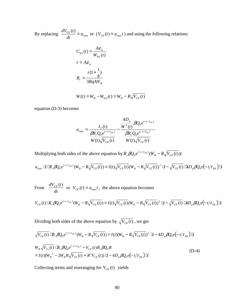
80
By replacing max
)(a
dt
tdVCE = or ( tatVCE max)( = ) and using the following relations:
)()()(
3
)1
1(
)()(
tVRWtWWtW
RqANb
rR
Ar
tW
AtC
CEBbcjB
Br
si
bcj
sibcj
−=−=
+=
=
=
ε
ε
equation (D-3) becomes
)()(
)(
4
)()(
)()/(
0
)/(02
)/(0
max
tVtW
eQR
eQtW
D
tVtW
eQR
tIa
CE
tr
tp
CE
tr
T
HL
HL
HL τ
τ
τ β
β
β −
−
− −=
Multiplying both sides of the above equation by ttVRWeQR CEBt
rHL ))(()/(
0 −− τβ
( ) tteQDtVttVRWtVtItVRWeQRta HLpCECEBCECEBt
rHL ⋅−⋅−⋅−=−⋅⋅ − τββ τ
02)/(
0max 4)())(()()())((
From dt
tdVCE )( or tatVCE max)( = , the above equation becomes
( ) tteQDtVttVRWtVtItVRWeQRtV HLpCECEBCECEBt
rCEHL ⋅−⋅−⋅−=−⋅ − τββ τ
02)/(
0 4)())(()()())(()(
Dividing both sides of the above equation by )(tVCE , we get
( ) tteQDttVRWtItVRWeQRtV HLpCEBCEBt
rCEHL ⋅−−⋅−=−⋅ − τββ τ
02)/(
0 4))()(())(()(
( ) tteQDttVRtVRWWtI
RQRtVeQRtVW
HLpCECEBB
rCEt
rCeBHL
⋅−−⋅+−=
−⋅ −
τβ
ββ τ
022
0)/(
0
4))()(2)((
)()( (D-4)
Collecting terms and rearranging for )(tVCE yields

81
( )
( ) 0)4)(()())(2
()())((
02
02)/(
0
=⋅−+−+⋅+
+⋅− −−
tteQDWtItVtRWtI
eQRWtVtRtIeQRR
HLpBTCEB
trBCeT
tr
HLHL
τβ
ββ ττ
Multiplying by the negative sign and rearranging to get
( )
( ) 0)4)(()())(2
()())((
02
0)/(
0
=⋅−−+⋅
+−⋅+ −−
tteQDWtItVtRtI
eQRWtVtRtIeQRR
HLpBTCE
trBCET
tr
HLHL
τβ
ββ ττ
(D-5)
Using the notations below
( )
( )
( ))4)((
))(2(
))((
02
0
0
HL
HL
HL
tpBTC
Tt
rBB
Tt
rA
eQDWtIR
tRtIeQRWR
tRtIeQRRR
τ
τ
τ
β
β
β
−
−
−
−=
⋅+=
⋅+=
the discriminant = )4(4 22CAB RtRRacb ⋅−=− , then equation (D-5) becomes
0)()()(
0)()(
=⋅+−
=⋅+−
tRtVRtVtVR
tRtVRtVR
CCEBCECEA
CCEBCEA
and has the solution of the form
A
CABB
A
CABBCE
R
tRRRR
R
tRRRRtV
2
4
2
4)()()(
2
2
⋅−−±=
⋅−−±−−=
Squaring the above equation, we get the final analytical form
2
222
4
442)(
A
CABCABBBCE R
tRRRtRRRRRtV
⋅−+⋅−±=
2
22
2
42)(
A
CABBCABCE R
tRRRRtRRRtV
⋅−±⋅−=

82
2
22
2
42)(
A
CABBCABCE R
tRRRRtRRRtV
⋅−−⋅−= (D-6)
where
)4)((
).)(2(
).)((
)/(0
2
)/(0
)/(0
HL
HL
HL
tpTBC
trBB
trA
eQDtIWR
tRtIeQRWR
tRtIeQRRR
τ
τ
τ
β
β
β
−
−
−
−=
+=
+=
Equation (D-6) is the analytical form of equation (4-15) and can be easily plotted for
different lifetime with the appropriate maxa value.

83
Figure 22 )0(
)0(−
+
T
T
I
I as a function of the bus voltage and lifetime through the ratio of
LtW )( .

84
Figure 23 Saber software simulation for )0( +TI as a function of busV and HLτ .

BIBLIOGRAPHY
86
BIBLIOGRAPHY
1. Baliga B.J., “Power Semiconductor Devices”, PWS Publishers, ch. 8, Boston (1996). 2. A.R. Hefner and D.L. Blackburn, “An Analytical Model for the Steady State and Transient Characteristics of the Power Insulated-Gate Bipolar Transistor”, Solid-State Electronics Vol.31, pp. 1513-1532, 1988. 3. A.R. Hefner, “Analytical Modeling of Device-Circuit Interactions for the Power Insulated Gate Bipolar Transistor (IGBT)”, IEEE Transactions on Industry Applications, Vol.26, No.6, Nov/Dec 1990. 4. Malay Trivedi, Krishna Shenai, “Modeling the Turn-OFF of IGBT’s in Hard and Soft-Switching Applications”, IEEE Transactions on Electron Devices, vol.44, pp.887-893, May 1997.
5. A. Ramamurthy, S. Sawant, and B.J. Baliga,”Modeling the
dt
dV of the IGBT
during Inductive Turn-OFF”, IEEE Transactions on Power Electronics, Vol.14, No.4, July 1999. 6. B. Fatemizadeh and D. Silber, “A Versatile Model for IGBT including Thermal Effects”, th24 IEEE Power Electronics Specialists Conf. (PESC’93), Seattle, USA, June 20-25, 1993, pp. 85-92. 7. Y. Yue, J.J. Liou, and I. Batarseh, “A Steady-State and Transient Model Valid for all Free-Carrier Injection Conditions”, th12 IEEE Applied power Electronics 1997. 8. J. Sgg, P. Tuerkes and R. Kraus, “Parameter Extraction Methodology and Validation for an Electro-Thermal Physics-Based NPT IGBT Model”, IEEE Industry Applications Society Annual Meeting, New Orleans, Louisiana, October 1997, pp. 1166-1173. 9. D.S. Kuo, C. Hu, and S.P. Sapp, “An Analytical Model for the Power Bipolar MOS Transistor”, Solid-State Electronics, Vol.29, No.12, pp. 1229-1237, 1986. 10. K. Sheng, S.J. Finney, and B.W. Williams, “A new Analytical IGBT Model with Improved Electrical Characteristics”, IEEE Transactions on Power Electronics, Vol.14, pp.98-107, Jan. 1999. 11. K. Sheng, Barry W. Williams and Stephen J. Finney, “A Review of IGBT Models”, IEEE Transactions on Power Electronics, Vol.15, No.6, November 2000, pp. 1250-1266.
87
12. Philippe Luturcq,” A Study of Distributed Switching Processes in IGBTs and Other Power Bipolar Devices”, IEEE th28 Annual Power Electronics Specialists Conference, Vol.1, pp. 139-147, 1997. 13. Naresh Thapar and Baliga, Jayant B., “An experimental Evaluation of the On-State Performance of the Trench IGBT Designs”, Solid-State Electronics Vol. 42, No. 5, pp. 771-776, 1998. 14. Udrea F. and Amartunga G.S.J., “An On-State Analytical Model for the Trench IGBT”, Solid-State Electronics Vol. 41, No. 8, pp. 1111-1118, 1997. 15. Chong-Man Yun Doo, Young Kim, Min-koo Han and Yearn-Ik Choi, ”Numerical Analysis of a New Vertical IGBT Structure with Reduced JFET Effect”, Solid-State Electronics Vol. 39, No. 8, pp. 1179-1183, 1996. 16. Robinson Andrew L., Pattanayak Deva N., adler, Michael S., baliga, B. Jayan, and wildi, Eric J., “Lateral Insulated Gate Transistors with Improved Latchup Characteristics”, IEEE Device Letters, Vol. EDL-7, No. 2, February, 1986. 17. Darwish M. and Board K., “Lateral Resurfed COMFET”, Electronics Letters, Vol. 20, No. 12, pp. 519-520, 1984. 18. Deva N. Pattanayak, A.L. Robinson, T. Paul Chow, Michael S. Adler, B. Jayant Baliga and Eric J. Wildi, “n-Channel Lateral Insulated Gate Transistors: Part I- Steady-State Characteristics”, IEEE Trans. On Electron Devices, Vol. ED-33, No. 12, pp. 1956-1963, 1986. 19. Fossum Jenny G. and Kim Yeong-Seuk, “static and Dynamic Latchup in the LIGBT”, IEEE Trans. On Electron Devices, Vol. 35, N0. 11, pp. 1977-1985, 1998. 20. Vellvehi M., Godignon P., Flores D., Fernandez J., Hidalgo S., Rebollo J. and Millan J., “A New Lateral IGBT for High Temperature Operation”, Solid-State Electronics Vol. 41, No. 5, pp. 793-747, 1997. 21. Ravishankar S. and B. Jayant Baliga, “Analysis of On-State Carrier Distribution in the DI-LIGBT”, Solid-State Electronics, Vol. 41, No. 5, pp. 733-738, 1997. 22. Sunkavalli Ravishankar and Baliga B. Jayant, “Composition of High Speed DI-LIGBT Structures”, Solid-State Electronics, Vol. 41, No. 12, pp. 1953-1956, 1997. 23. Huang Qun and Amaratunga Gehan, “Forward Blocking Capability of Double Gate IGBTs at High Temperatures”, Solid-State Electronics, Vol. 38, No. 5, pp. 981-982, 1995.

88
24. Robert F. Pierret, “Semiconductor Device Fundamentals”, Addison-Wesley Publishing Company, Inc, pp. 75-148, 1996. 25. Ben G. Streetman, “Solid State Electronic Devices”, Prentice-Hall, Inc., Englewood Cliffs, New Jersey (1980), chaprter11. 26. MATLAB User’s Manual.