Embed Size (px)
Citation preview

TPS7A4001
OUT
FBGND
CIN
R1
CBYP
COUT
IN
EN
VIN
VOUT
R2
VEN
VIN
100 V
Product
Folder
Sample &Buy
Technical
Documents
Tools &
Software
Support &Community
ReferenceDesign
TPS7A4001SBVS162B –MARCH 2011–REVISED JULY 2015
TPS7A4001 100-V Input Voltage, 50-mA, Very High Voltage Linear Regulator1 Features 3 Description
The TPS7A4001 device is a very high voltage-1• Very High Maximum Input Voltage: 100 V
tolerant linear regulator that offers the benefits of a• Wide Input Voltage Range: 7 to 100 V thermally-enhanced package (HVSSOP), and is able• Accuracy: to withstand continuous DC or transient input
voltages of up to 100 V.– Nominal: 1%– Over Line, Load, and Temperature: 2.5% The TPS7A4001 device is stable with any output
capacitance greater than 4.7 µF and any input• Low Quiescent Current: 25 µAcapacitance greater than 1 µF (over temperature and• Quiescent Current at Shutdown: 4.1 µA tolerance). Therefore, implementations of this device
• Maximum Output Current: 50 mA require minimal board space because of itsminiaturized packaging (HVSSOP) and a potentially• CMOS Logic-Level-Compatible Enable Pinsmall output capacitor. In addition, the TPS7A4001• Adjustable Output Voltage from about 1.175 todevice offers an enable pin (EN) compatible with90 V standard CMOS logic to enable a low-current
• Stable With Ceramic Capacitors: shutdown mode.– Input Capacitance: ≥1 µF The TPS7A4001 device has an internal thermal– Output Capacitance: ≥4.7 µF shutdown and current limiting to protect the system
during fault conditions. The HVSSOP packages has• Dropout Voltage: 290 mVan operating temperature range of TJ = –40°C to• Built-In Current Limit and Thermal Shutdown 125°C.ProtectionIn addition, the TPS7A4001 device is ideal for• Package: High Thermal Performance HVSSOPgenerating a low-voltage supply from intermediatePowerPAD™voltage rails in telecom and industrial applications;
• Operating Temperature Range: –40°C to 125°C not only can it supply a well-regulated voltage rail, butit can also withstand and maintain regulation during
2 Applications very high and fast voltage transients. These featurestranslate to simpler and more cost-effective electrical• Microprocessors, Microcontrollers Powered bysurge-protection circuitry for a wide range ofIndustrial Busses With High Voltage Transients applications, including PoE, bias supply, and LED
• Industrial Automation lighting.• Telecom Infrastructure
Device Information(1)• Automotive
PART NUMBER PACKAGE BODY SIZE (NOM)• Power over Ethernet (PoE)TPS7A4001 HVSSOP (8) 3.00 mm × 5.00 mm• LED Lighting(1) For all available packages, see the orderable addendum at• Bias Power Supplies the end of the data sheet.
Typical Application Schematic
1
An IMPORTANT NOTICE at the end of this data sheet addresses availability, warranty, changes, use in safety-critical applications,intellectual property matters and other important disclaimers. PRODUCTION DATA.

TPS7A4001SBVS162B –MARCH 2011–REVISED JULY 2015 www.ti.com
Table of Contents7.4 Device Functional Modes.......................................... 91 Features .................................................................. 1
8 Application and Implementation ........................ 102 Applications ........................................................... 18.1 Application Information............................................ 103 Description ............................................................. 18.2 Typical Application ................................................. 114 Revision History..................................................... 2
9 Power Supply Recommendations ...................... 125 Pin Configuration and Functions ......................... 310 Layout................................................................... 136 Specifications......................................................... 4
10.1 Layout Guidelines ................................................. 136.1 Absolute Maximum Ratings ..................................... 410.2 Layout Example .................................................... 136.2 ESD Ratings.............................................................. 410.3 Thermal Considerations ........................................ 136.3 Recommended Operating Conditions....................... 410.4 Power Dissipation ................................................. 146.4 Thermal Information .................................................. 4
11 Device and Documentation Support ................. 156.5 Electrical Characteristics........................................... 511.1 Community Resources.......................................... 156.6 Typical Characteristics .............................................. 611.2 Trademarks ........................................................... 157 Detailed Description .............................................. 811.3 Electrostatic Discharge Caution............................ 157.1 Overview ................................................................... 811.4 Glossary ................................................................ 157.2 Functional Block Diagram ......................................... 8
12 Mechanical, Packaging, and Orderable7.3 Feature Description................................................... 8Information ........................................................... 15
4 Revision HistoryNOTE: Page numbers for previous revisions may differ from page numbers in the current version.
Changes from Revision A (March 2011) to Revision B Page
• Added ESD Ratings table, Feature Description section, Device Functional Modes, Application and Implementationsection, Power Supply Recommendations section, Layout section, Device and Documentation Support section, andMechanical, Packaging, and Orderable Information section. ................................................................................................ 1
• Changed Package from MSOP-8 to HVSSOP. ..................................................................................................................... 1• Changed TJ value for disabled mode operating mode from 165 to 170°C............................................................................. 9• Changed value from 35 to 45°C ........................................................................................................................................... 14
Changes from Original (March 2011) to Revision A Page
• Changed all 105 V to 100 V on page 1 .................................................................................................................................. 1
2 Submit Documentation Feedback Copyright © 2011–2015, Texas Instruments Incorporated
Product Folder Links: TPS7A4001

2
1
3
4
7
8
6
5
FB
NC
GND
OUT
EN
NC
NC
IN
TPS7A4001www.ti.com SBVS162B –MARCH 2011–REVISED JULY 2015
5 Pin Configuration and Functions
DGN Package8-Pin HVSSOP
Top View
Pin FunctionsPIN
I/O DESCRIPTIONNAME NO.
OUT 1 O Regulator output. A capacitor > 4.7 µF must be tied from this pin to ground to assure stability.FB 2 O This pin is the input to the control-loop error amplifier. It is used to set the output voltage of the device.
3NC 6 — Not internally connected. This pin must either be left open or tied to GND.
7GND 4 — Ground
This pin turns the regulator on or off.If VEN ≥ VEN_HI the regulator is enabled.EN 5 I If VEN ≤ VEN_LO, the regulator is disabled.If not used, the EN pin can be connected to IN. Make sure that VEN ≤ VIN at all times.
IN 8 I Input supplySolder to printed-circuit-board (PCB) to enhance thermal performance.
PowerPAD — — NOTE: The PowerPAD is internally connected to GND.Although it can be left floating, TI highly recommends connecting the PowerPAD to the GND plane.
Copyright © 2011–2015, Texas Instruments Incorporated Submit Documentation Feedback 3
Product Folder Links: TPS7A4001

TPS7A4001SBVS162B –MARCH 2011–REVISED JULY 2015 www.ti.com
6 Specifications
6.1 Absolute Maximum Ratingsover operating junction temperature range (unless otherwise noted) (1)
MIN MAX UNITIN pin to GND pin –0.3 105OUT pin to GND pin –0.3 105OUT pin to IN pin –105 0.3
Voltage FB pin to GND pin –0.3 2 VFB pin to IN pin –105 0.3EN pin to IN pin –105 0.3EN pin to GND pin –0.3 105
Current Peak output Internally limitedOperating virtual junction, TJ –40 125
Temperature °CStorage, Tstg –65 150
(1) Stresses beyond those listed under Absolute Maximum Ratings may cause permanent damage to the device. These are stress ratingsonly, which do not imply functional operation of the device at these or any other conditions beyond those indicated under RecommendedOperating Conditions. Exposure to absolute-maximum-rated conditions for extended periods may affect device reliability.
6.2 ESD RatingsVALUE UNIT
Human-body model (HBM), per ANSI/ESDA/JEDEC JS-001 (1) ±2500V(ESD) Electrostatic discharge VCharged-device model (CDM), per JEDEC specification JESD22- ±500C101 (2)
(1) JEDEC document JEP155 states that 500-V HBM allows safe manufacturing with a standard ESD control process.(2) JEDEC document JEP157 states that 250-V CDM allows safe manufacturing with a standard ESD control process.
6.3 Recommended Operating Conditionsover operating junction temperature range (unless otherwise noted)
MIN NOM MAX UNITVIN 7 100 VVOUT 1.161 90 VVEN 0 100 VIOUT 0 50 mA
6.4 Thermal InformationTPS7A4001
THERMAL METRIC (1) DGN (HVVSOP) UNIT8 PINS
RθJA Junction-to-ambient thermal resistance 66.7 °C/WRθJC(top) Junction-to-case (top) thermal resistance 54.1 °C/WRθJB Junction-to-board thermal resistance 38.1 °C/WψJT Junction-to-top characterization parameter 2 °C/WψJB Junction-to-board characterization parameter 37.8 °C/WRθJC(bot) Junction-to-case (bottom) thermal resistance 15.5 °C/W
(1) For more information about traditional and new thermal metrics, see the Semiconductor and IC Package Thermal Metrics applicationreport, SPRA953.
4 Submit Documentation Feedback Copyright © 2011–2015, Texas Instruments Incorporated
Product Folder Links: TPS7A4001

D%VOUT
DIOUT
D%VOUT
DVIN
TPS7A4001www.ti.com SBVS162B –MARCH 2011–REVISED JULY 2015
6.5 Electrical CharacteristicsAt TJ = –40°C to 125°C, VIN = VOUT(NOM) + 2 V or VIN = 7 V (whichever is greater), VEN = VIN, IOUT = 100 µA, CIN = 1 μF, COUT = 4.7 μF, andFB tied to OUT, unless otherwise noted.
PARAMETER TEST CONDITIONS MIN TYP MAX UNITVIN Input voltage 7 100 VVREF Internal reference TJ = 25°C, VFB = VREF, VIN = 9 V, IOUT = 25 mA 1.161 1.173 1.185 V
Output voltage range (1) VIN ≥ VOUT(NOM) + 2 V VREF 90 VNominal accuracy TJ = 25°C, VIN = 9 V, IOUT = 25 mA –1 1 %VOUTVOUT
VOUT(NOM) + 2 V ≤ VIN ≤ 24 V (2)Overall accuracy –2.5 2.5 %VOUT100 µA ≤ IOUT ≤ 50 mA
Line regulation 7 V ≤ VIN ≤ 100 V 0.03 %VOUT
Load regulation 100 µA ≤ IOUT ≤ 50 mA 0.31 %VOUT
VIN = 17 V, VOUT(NOM) = 18 V, IOUT = 20 mA 290 mVVDO Dropout voltage
VIN = 17 V, VOUT(NOM) = 18 V, IOUT = 50mA 0.78 1.3 VVOUT = 90% VOUT(NOM), VIN = 7 V, TJ ≤ 85°C 51 117 200 mA
ILIM Current limitVOUT = 90% VOUT(NOM), VIN = 9 V 51 128 200 mA7 V ≤ VIN ≤ 100 V, IOUT = 0 mA 25 65 μA
IGND Ground currentIOUT = 50 mA 25 μA
ISHDN Shutdown supply current VEN = 0.4 V 4.1 20 μAIFB Feedback current (3) –0.1 0.01 0.1 µAIEN Enable current 7 V ≤ VIN ≤ 100 V, VIN = VEN 0.02 1 μAVEN_HI Enable high-level voltage 1.5 VIN VVEN_LO Enable low- level voltage 0 0.4 V
VIN = 12 V, VOUT(NOM) = VREF, COUT = 10 μF, 58 μVRMSBW = 10 Hz to 100 kHzVNOISE Output noise voltage
VIN = 12 V, VOUT(NOM) = 5 V, COUT = 10 μF, 73 μVRMSCBYP(4) = 10 nF, BW = 10 Hz to 100 kHz
VIN = 12 V, VOUT(NOM) = 5 V, COUT = 10 μF,PSRR Power-supply rejection ratio 65 dBCBYP(4) = 10 nF, ƒ = 100 Hz
Shutdown, temperature increasing 170 °CTSD Thermal shutdown temperature
Reset, temperature decreasing 150 °CTJ Operating junction temperature –40 125 °C
(1) To ensure stability at no-load conditions, a current from the feedback resistive network greater than or equal to 10μA is required.(2) Maximum input voltage is limited to 24 V because of the package power dissipation limitations at full load (P ≈ (VIN – VOUT) × IOUT = (24
V – VREF) × 50 mA ≈ 1.14 W). The device is capable of sourcing a maximum current of 50 mA at higher input voltages as long as thepower dissipated is within the thermal limits of the package plus any external heatsinking.
(3) IFB > 0 flows out of the device.(4) CBYP refers to a bypass capacitor connected to the FB and OUT pins.
Copyright © 2011–2015, Texas Instruments Incorporated Submit Documentation Feedback 5
Product Folder Links: TPS7A4001

0
10
20
30
40
50
60
70
80
90
100
−40 −25 −10 5 20 35 50 65 80 95 110 125Temperature (°C)
I FB (
nA)
0
20
40
60
80
100
5 15 25 35 45 55 65 75 85 95 105
Input Voltage (V)
Isu
b(G
ND
)
− 40°C
+ 25°C
+ 85°C
+ 105°C
+ 125°C
IOUT = 0mA
−10
−7.5
−5
−2.5
0
2.5
5
7.5
10
5 15 25 35 45 55 65 75 85 95 105Input Voltage (V)
VO
UT
(NO
M) (
%)
− 40°C+ 25°C+ 85°C
+ 105°C+ 125°C
1.075
1.125
1.175
1.225
1.275
5 15 25 35 45 55 65 75 85 95 105Input Voltage (V)
VF
B (
V)
− 40°C+ 25°C+ 85°C
+ 105°C+ 125°C
Time (1ms/div)
100mV/div
VIN
VOUT
VOUT100mV/div
C = 0nFBYP
C = 10nFBYP
V = 5V, I = 28mA,
V Slew Rate = 220V/ms
V = 12V 55V
C = 10 Fm
D ®
OUT
IN
OUT
IN
OUT
50V/div
Time (100 s/div)m
V = 12V, V = 5V
1mA
C = 10 F, C = 10nF
I = 1mA 29mAD ® ®
m
IN OUT
OUT BYP
OUT
IOUT
VOUT
10mA/div
50mV/div
TPS7A4001SBVS162B –MARCH 2011–REVISED JULY 2015 www.ti.com
6.6 Typical CharacteristicsAt TJ = –40°C to 125°C, VIN = VOUT(NOM) + 2 V or VIN = 9 V (whichever is greater), VEN = VIN, IOUT = 100 µA, CIN = 1 μF, COUT =4.7 μF, and FB tied to OUT, unless otherwise noted.
Figure 1. Line Transient Response vs CBYP Figure 2. Load Transient Response
Figure 3. Line Regulation Figure 4. Feedback Voltage
Figure 5. Ground Current vs Input Voltage Figure 6. Feedback Current
6 Submit Documentation Feedback Copyright © 2011–2015, Texas Instruments Incorporated
Product Folder Links: TPS7A4001

0
10
20
30
40
50
60
70
80
90
100
10 100 1k 10k 100k 1M 10MFrequency (Hz)
PS
RR
(dB
)
IOUT = 50mAIOUT = 100µA
VIN = 12VVOUT = 5VCOUT = 10µFCBYP = 10nF
0
40
80
120
160
200
6 9 12 15 18 21 24
Input Voltage (V)
I CL
(mA
)
− 40°C
+ 25°C
+ 85°C
+ 105°C
+ 125°C
0.001
0.01
0.1
1
10
10 100 1k 10k 100k 1M 10MFrequency (Hz)
Noi
se (
µV/
Hz
)
IOUT = 100µA,VNOISE = 60µVRMSIOUT = 50mA,VNOISE = 100µVRMS
VIN = 12VVOUT = VREFCOUT = 10µFCBYP = 10nF
0
0.5
1
1.5
2
2.5
−40 −25 −10 5 20 35 50 65 80 95 110 125
Vsub (EN_LO)
Vsub (EN_HI)
Temperature (°C)
VE
N(V
)
0
10
20
30
40
50
60
70
80
90
100
0 10 20 30 40 50Output Current (mA)
I GN
D (
µA)
− 40°C+ 25°C+ 85°C+ 105°C+ 125°C
0
0.25
0.5
0.75
1
1.25
1.5
1.75
2
0 10 20 30 40 50Output Current (mA)
VD
RO
P (
V)
− 40°C+ 25°C+ 85°C
+ 105°C+ 125°C
TPS7A4001www.ti.com SBVS162B –MARCH 2011–REVISED JULY 2015
Typical Characteristics (continued)At TJ = –40°C to 125°C, VIN = VOUT(NOM) + 2 V or VIN = 9 V (whichever is greater), VEN = VIN, IOUT = 100 µA, CIN = 1 μF, COUT =4.7 μF, and FB tied to OUT, unless otherwise noted.
Figure 7. Ground Current vs Output Voltage Figure 8. Dropout Voltage
Figure 9. Enable Threshold Voltage Figure 10. Output Spectral Noise Density
Figure 11. Current Limit Figure 12. Power-Supply Rejection Ratio
Copyright © 2011–2015, Texas Instruments Incorporated Submit Documentation Feedback 7
Product Folder Links: TPS7A4001

UVLO
Thermal
Shutdown
Current
Limit
EnableError
Amp
IN
EN
OUT
FB
Pass
Device
TPS7A4001SBVS162B –MARCH 2011–REVISED JULY 2015 www.ti.com
7 Detailed Description
7.1 OverviewThe TPS7A4001 device belongs to a new generation of linear regulators that use an innovative BiCMOS processtechnology to achieve very high maximum input and output voltages.
This process not only allows the TPS7A4001 device to maintain regulation during very fast high-voltagetransients up to 105 V, but it also allows the TPS7A4001 device to regulate from a continuous high-voltage inputrail. Unlike other regulators created using bipolar technology, the ground current of the TPS7A4001 device isalso constant over its output current range, resulting in increased efficiency and lower power consumption.
These features, combined with a high thermal performance HVSSOP PowerPAD package, make this deviceideal for industrial and telecom applications.
7.2 Functional Block Diagram
7.3 Feature Description
7.3.1 Internal Current LimitThe fixed internal current limit of the TPS7A4001 device helps protect the regulator during fault conditions. Themaximum amount of current the device can source is the current limit (309 mA, typical), and is largelyindependent of output voltage. For reliable operation, the device does not operate in current limit for extendedperiods of time.
7.3.2 Enable Pin OperationThe TPS7A4001 device provides an enable pin (EN) feature that turns on the regulator when VEN > VEN_HI, anddisables the regulator when VEN < VEN_LO.
7.3.3 Thermal ProtectionThermal protection disables the output when the junction temperature rises to approximately 170°C, allowing thedevice to cool. When the junction temperature cools to approximately 150°C, the output circuitry is enabled.Depending on power dissipation, thermal resistance, and ambient temperature, the thermal protection circuit maycycle on and off. This cycling limits the dissipation of the regulator, protecting it from damage as a result ofoverheating.
Any tendency to activate the thermal protection circuit indicates excessive power dissipation or an inadequateheatsink. For reliable operation, limit junction temperature to a maximum of 125°C. To estimate the margin ofsafety in a complete design (including heatsink), increase the ambient temperature until the thermal protection istriggered; use worst-case loads and signal conditions. For good reliability, trigger thermal protection at least 35°Cabove the maximum expected ambient condition of your particular application. This configuration produces aworst-case junction temperature of 125°C at the highest expected ambient temperature and worst-case load.
8 Submit Documentation Feedback Copyright © 2011–2015, Texas Instruments Incorporated
Product Folder Links: TPS7A4001

TPS7A4001www.ti.com SBVS162B –MARCH 2011–REVISED JULY 2015
Feature Description (continued)The internal protection circuitry of the TPS7A4001 device has been designed to protect against overloadconditions. The protection circuitry was not intended to replace proper heatsinking. Continuously running theTPS7A4001 device into thermal shutdown degrades device reliability.
7.3.4 Undervoltage Lockout (UVLO)The TPS7A4001 contains an Undervoltage Lockout comparator that ensures the error amplifier is disabled whenthe input voltage is below the required minimum operational voltage. The minimum recommended operationalvoltage is 7 V.
7.4 Device Functional Modes
7.4.1 Normal OperationThe device regulates to the nominal output voltage under the following conditions:• The input voltage is at least as high as VIN(min).• The input voltage is greater than the nominal output voltage added to the dropout voltage.• The enable voltage has previously exceeded the enable rising threshold voltage and has not decreased
below the enable falling threshold.• The output current is less than the current limit.• The device junction temperature is less than the maximum specified junction temperature.
7.4.2 Dropout OperationIf the input voltage is lower than the nominal output voltage plus the specified dropout voltage, but all otherconditions are met for normal operation, the device operates in dropout mode. In this mode of operation, theoutput voltage is the same as the input voltage minus the dropout voltage. The transient performance of thedevice is significantly degraded because the pass device (as a bipolar junction transistor, or BJT) is in saturationand no longer controls the current through the LDO. Line or load transients in dropout can result in large outputvoltage deviations.
7.4.3 DisabledThe device is disabled under the following conditions:• The enable voltage is less than the enable falling threshold voltage or has not yet exceeded the enable rising
threshold.• The device junction temperature is greater than the thermal shutdown temperature.
Table 1 lists the conditions that lead to the different modes of operation.
Table 1. Device Functional Mode ComparisonPARAMETER
OPERATING MODEVIN VEN IOUT TJ
VIN > VOUT(nom) + VDO andNormal mode VEN > VEN_HI IOUT < ILIM T J < 125°CVIN > VIN(min)
Dropout mode VIN(min) < VIN < VOUT(nom) + VDO VEN > VEN_HI — TJ < 125°CDisabled mode — VEN < VEN_LO — TJ > 170°C(any true condition disables the device)
Copyright © 2011–2015, Texas Instruments Incorporated Submit Documentation Feedback 9
Product Folder Links: TPS7A4001
VOUT
VREF
- 1R = R1 2
VOUT
R + R1 2
³ 10 Am, where
TPS7A4001
OUT
FBGND
C
10 µFIN
R1
C
10 nFBYP
C
10 FOUT
µ
IN
EN
VINVOUT
R2
TPS7A4001SBVS162B –MARCH 2011–REVISED JULY 2015 www.ti.com
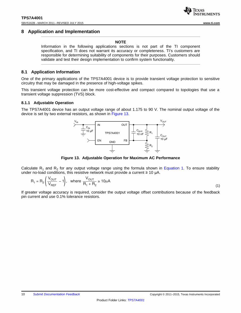
8 Application and Implementation
NOTEInformation in the following applications sections is not part of the TI componentspecification, and TI does not warrant its accuracy or completeness. TI’s customers areresponsible for determining suitability of components for their purposes. Customers shouldvalidate and test their design implementation to confirm system functionality.
8.1 Application InformationOne of the primary applications of the TPS7A4001 device is to provide transient voltage protection to sensitivecircuitry that may be damaged in the presence of high-voltage spikes.
This transient voltage protection can be more cost-effective and compact compared to topologies that use atransient voltage suppression (TVS) block.
8.1.1 Adjustable OperationThe TPS7A4001 device has an output voltage range of about 1.175 to 90 V. The nominal output voltage of thedevice is set by two external resistors, as shown in Figure 13.
Figure 13. Adjustable Operation for Maximum AC Performance
Calculate R1 and R2 for any output voltage range using the formula shown in Equation 1. To ensure stabilityunder no-load conditions, this resistive network must provide a current ≥ 10 μA.
(1)
If greater voltage accuracy is required, consider the output voltage offset contributions because of the feedbackpin current and use 0.1% tolerance resistors.
10 Submit Documentation Feedback Copyright © 2011–2015, Texas Instruments Incorporated
Product Folder Links: TPS7A4001

Where:VOUT
R + R1 2
≥10 µA, and
VOUT
VREF
– 1R = R1 2
TPS7A4001
OUT
FBGND
C
10 µFIN
R1
C
10 nFBYP
C
10 FOUT
µ
IN
EN
VIN VOUT
R2
VEN
TPS7A4001www.ti.com SBVS162B –MARCH 2011–REVISED JULY 2015
8.2 Typical Application
Figure 14. Example Circuit to Maximize Transient Performance
8.2.1 Design RequirementsFor this design example, use the following parameters listed in Table 2.
Table 2. Design ParametersPARAMETER VALUE
VIN 12 V, with 55 V surge toleranceVOUT 5 V (ideal), 4.981 (actual)IOUT 28 mA
Accuracy 5 %R1, R2 162 kΩ, 49.9 kΩ
8.2.2 Detailed Design ProcedureThe maximum value of total feedback resistance can be calculated to be 500 kΩ. Equation 1 was used tocalculate R1 and R2, and standard 1% resistors were selected to keep the accuracy within the 5% allocation. 10-uF ceramic input and output capacitors were selected, along with a 10-nF bypass capacitor for optimal ACperformance.
8.2.2.1 Capacitor RecommendationsLow equivalent series resistance (ESR) capacitors should be used for the input, output, and bypass capacitors.Ceramic capacitors with X7R and X5R dielectrics are required. Ceramic X7R capacitors offer improved voltageand temperature coefficients, while ceramic X5R capacitors are the most cost-effective and are available inhigher values.
NOTEHigh ESR capacitors may degrade PSRR.
8.2.2.2 Input and Output Capacitor RequirementsThe TPS7A4001 device high voltage linear regulator achieves stability with a minimum output capacitance of 4.7µF and input capacitance of 1 µF; however, TI highly recommends to use 10-μF output and input capacitors tomaximize AC performance.
8.2.2.3 Bypass Capacitor RequirementsAlthough a bypass capacitor (CBYP) is not needed to achieve stability, TI highly recommends using a 10-nFbypass capacitor to maximize AC performance (including line transient, noise, and PSRR). For additionalinformation regarding the performance improvements of using a bypass capacitor, see .
8.2.2.4 Transient ResponseAs with any regulator, increasing the size of the output capacitor reduces overshoot and undershoot magnitudebut increases the duration of the transient response.
The presence of the CBYP capacitor may greatly improve the line transient response of the TPS7A4001 device,as shown in Figure 1.
Copyright © 2011–2015, Texas Instruments Incorporated Submit Documentation Feedback 11
Product Folder Links: TPS7A4001

Time (1ms/div)
100mV/div
VIN
VOUT
VOUT100mV/div
C = 0nFBYP
C = 10nFBYP
V = 5V, I = 28mA,
V Slew Rate = 220V/ms
V = 12V 55V
C = 10 Fm
D ®
OUT
IN
OUT
IN
OUT
50V/div
Time (100 s/div)m
V = 12V, V = 5V
1mA
C = 10 F, C = 10nF
I = 1mA 29mAD ® ®
m
IN OUT
OUT BYP
OUT
IOUT
VOUT
10mA/div
50mV/div
TPS7A4001SBVS162B –MARCH 2011–REVISED JULY 2015 www.ti.com
8.2.3 Application Curves
Figure 15. Line Transient Response vs CBYP Figure 16. Load Transient Response
9 Power Supply RecommendationsThe input supply for the LDO should not exceed its recommended operating conditions (7 V to 100 V). The inputvoltage should provide adequate headroom for the device to have a regulated output. If the input supply is noisy,additional input capacitors with low ESR can help improve the output noise performance. The input and outputsupplies should also be bypassed with 10-µF capacitors located near the input and output pins. There should beno other components located between these capacitors and the pins.
12 Submit Documentation Feedback Copyright © 2011–2015, Texas Instruments Incorporated
Product Folder Links: TPS7A4001

1
2
3
4
8
7
6
5
OUT
FB
NC
GND
IN
NC
EN
Input GND Plane
Output GND Plane
VinThermal
Pad
Cout
R2
Sense Line
Vout
Cin
R1
NC
TPS7A4001www.ti.com SBVS162B –MARCH 2011–REVISED JULY 2015
10 Layout
10.1 Layout Guidelines
10.1.1 Board Layout Recommendations to Improve PSRR and Noise PerformanceTo improve AC performance such as PSRR, output noise, and transient response, TI recommends designing theboard with separate ground planes for IN and OUT, with each ground plane connected only at the GND pin ofthe device. In addition, the ground connection for the output capacitor should connect directly to the GND pin ofthe device.
Equivalent series inductance (ESL) and ESR must be minimized to maximize performance and ensure stability.Every capacitor (CIN, COUT, CBYP) must be placed as close as possible to the device and on the same side of thePCB as the regulator itself.
Do not place any of the capacitors on the opposite side of the PCB from where the regulator is installed. The useof vias and long traces is strongly discouraged because they may impact system performance negatively andeven cause instability.
If possible, and to ensure the maximum performance denoted in this product data sheet, use the same layoutpattern used for the TPS7A40 evaluation board, available at www.ti.com.
10.2 Layout Example
Figure 17. Recommended Layout Example
10.3 Thermal ConsiderationsThermal protection disables the output when the junction temperature rises to approximately 170°C, allowing thedevice to cool. When the junction temperature cools to approximately 150°C, the output circuitry is enabled.Depending on power dissipation, thermal resistance, and ambient temperature, the thermal protection circuit maycycle ON and OFF. This cycling limits the dissipation of the regulator, protecting it from damage as a result ofoverheating.
Copyright © 2011–2015, Texas Instruments Incorporated Submit Documentation Feedback 13
Product Folder Links: TPS7A4001

P = (V V ) I-D IN OUT OUT
TPS7A4001SBVS162B –MARCH 2011–REVISED JULY 2015 www.ti.com
Thermal Considerations (continued)Any tendency to activate the thermal protection circuit indicates excessive power dissipation or an inadequateheatsink. For reliable operation, junction temperature should be limited to a maximum of 125°C. To estimate themargin of safety in a complete design (including heatsink), increase the ambient temperature until the thermalprotection is triggered; use worst-case loads and signal conditions. For good reliability, thermal protection shouldtrigger at least 45°C above the maximum expected ambient condition of the particular application. Thisconfiguration produces a worst-case junction temperature of 125°C at the highest expected ambient temperatureand worst-case load.
The internal protection circuitry of the TPS7A4001 has been designed to protect against overload conditions. Itwas not intended to replace proper heatsinking. Continuously running the TPS7A4001 device into thermalshutdown degrades device reliability.
10.4 Power DissipationThe ability to remove heat from the die is different for each package type, presenting different considerations inthe PCB layout. The PCB area around the device that is free of other components moves the heat from thedevice to the ambient air. Using heavier copper increases the effectiveness in removing heat from the device.The addition of plated through-holes to heat dissipating layers also improves the heatsink effectiveness.
Power dissipation depends on input voltage and load conditions. Power dissipation (PD) is equal to the product ofthe output current times the voltage drop across the output pass element, as shown in Equation 2:
(2)
14 Submit Documentation Feedback Copyright © 2011–2015, Texas Instruments Incorporated
Product Folder Links: TPS7A4001

TPS7A4001www.ti.com SBVS162B –MARCH 2011–REVISED JULY 2015
11 Device and Documentation Support
11.1 Community ResourcesThe following links connect to TI community resources. Linked contents are provided "AS IS" by the respectivecontributors. They do not constitute TI specifications and do not necessarily reflect TI's views; see TI's Terms ofUse.
TI E2E™ Online Community TI's Engineer-to-Engineer (E2E) Community. Created to foster collaborationamong engineers. At e2e.ti.com, you can ask questions, share knowledge, explore ideas and helpsolve problems with fellow engineers.
Design Support TI's Design Support Quickly find helpful E2E forums along with design support tools andcontact information for technical support.
11.2 TrademarksPowerPAD, E2E are trademarks of Texas Instruments.All other trademarks are the property of their respective owners.
11.3 Electrostatic Discharge CautionThese devices have limited built-in ESD protection. The leads should be shorted together or the device placed in conductive foamduring storage or handling to prevent electrostatic damage to the MOS gates.
11.4 GlossarySLYZ022 — TI Glossary.
This glossary lists and explains terms, acronyms, and definitions.
12 Mechanical, Packaging, and Orderable InformationThe following pages include mechanical, packaging, and orderable information. This information is the mostcurrent data available for the designated devices. This data is subject to change without notice and revision ofthis document. For browser-based versions of this data sheet, refer to the left-hand navigation.
Copyright © 2011–2015, Texas Instruments Incorporated Submit Documentation Feedback 15
Product Folder Links: TPS7A4001

PACKAGE OPTION ADDENDUM
www.ti.com 19-Mar-2015
Addendum-Page 1
PACKAGING INFORMATION
Orderable Device Status(1)
Package Type PackageDrawing
Pins PackageQty
Eco Plan(2)
Lead/Ball Finish(6)
MSL Peak Temp(3)
Op Temp (°C) Device Marking(4/5)
Samples
TPS7A4001DGNR ACTIVE MSOP-PowerPAD
DGN 8 2500 Green (RoHS& no Sb/Br)
CU NIPDAU Level-2-260C-1 YEAR -40 to 125 QVQ
TPS7A4001DGNT ACTIVE MSOP-PowerPAD
DGN 8 250 Green (RoHS& no Sb/Br)
CU NIPDAU Level-2-260C-1 YEAR -40 to 125 QVQ
(1) The marketing status values are defined as follows:ACTIVE: Product device recommended for new designs.LIFEBUY: TI has announced that the device will be discontinued, and a lifetime-buy period is in effect.NRND: Not recommended for new designs. Device is in production to support existing customers, but TI does not recommend using this part in a new design.PREVIEW: Device has been announced but is not in production. Samples may or may not be available.OBSOLETE: TI has discontinued the production of the device.
(2) Eco Plan - The planned eco-friendly classification: Pb-Free (RoHS), Pb-Free (RoHS Exempt), or Green (RoHS & no Sb/Br) - please check http://www.ti.com/productcontent for the latest availabilityinformation and additional product content details.TBD: The Pb-Free/Green conversion plan has not been defined.Pb-Free (RoHS): TI's terms "Lead-Free" or "Pb-Free" mean semiconductor products that are compatible with the current RoHS requirements for all 6 substances, including the requirement thatlead not exceed 0.1% by weight in homogeneous materials. Where designed to be soldered at high temperatures, TI Pb-Free products are suitable for use in specified lead-free processes.Pb-Free (RoHS Exempt): This component has a RoHS exemption for either 1) lead-based flip-chip solder bumps used between the die and package, or 2) lead-based die adhesive used betweenthe die and leadframe. The component is otherwise considered Pb-Free (RoHS compatible) as defined above.Green (RoHS & no Sb/Br): TI defines "Green" to mean Pb-Free (RoHS compatible), and free of Bromine (Br) and Antimony (Sb) based flame retardants (Br or Sb do not exceed 0.1% by weightin homogeneous material)
(3) MSL, Peak Temp. - The Moisture Sensitivity Level rating according to the JEDEC industry standard classifications, and peak solder temperature.
(4) There may be additional marking, which relates to the logo, the lot trace code information, or the environmental category on the device.
(5) Multiple Device Markings will be inside parentheses. Only one Device Marking contained in parentheses and separated by a "~" will appear on a device. If a line is indented then it is a continuationof the previous line and the two combined represent the entire Device Marking for that device.
(6) Lead/Ball Finish - Orderable Devices may have multiple material finish options. Finish options are separated by a vertical ruled line. Lead/Ball Finish values may wrap to two lines if the finishvalue exceeds the maximum column width.
Important Information and Disclaimer:The information provided on this page represents TI's knowledge and belief as of the date that it is provided. TI bases its knowledge and belief on informationprovided by third parties, and makes no representation or warranty as to the accuracy of such information. Efforts are underway to better integrate information from third parties. TI has taken andcontinues to take reasonable steps to provide representative and accurate information but may not have conducted destructive testing or chemical analysis on incoming materials and chemicals.TI and TI suppliers consider certain information to be proprietary, and thus CAS numbers and other limited information may not be available for release.

PACKAGE OPTION ADDENDUM
www.ti.com 19-Mar-2015
Addendum-Page 2
In no event shall TI's liability arising out of such information exceed the total purchase price of the TI part(s) at issue in this document sold by TI to Customer on an annual basis.
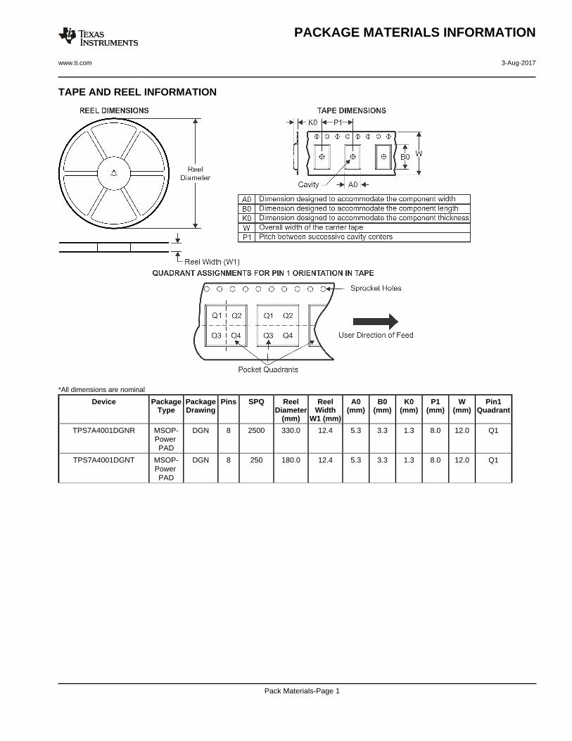
TAPE AND REEL INFORMATION
*All dimensions are nominal
Device PackageType
PackageDrawing
Pins SPQ ReelDiameter
(mm)
ReelWidth
W1 (mm)
A0(mm)
B0(mm)
K0(mm)
P1(mm)
W(mm)
Pin1Quadrant
TPS7A4001DGNR MSOP-Power PAD
DGN 8 2500 330.0 12.4 5.3 3.3 1.3 8.0 12.0 Q1
TPS7A4001DGNT MSOP-Power PAD
DGN 8 250 180.0 12.4 5.3 3.3 1.3 8.0 12.0 Q1
PACKAGE MATERIALS INFORMATION
www.ti.com 3-Aug-2017
Pack Materials-Page 1

*All dimensions are nominal
Device Package Type Package Drawing Pins SPQ Length (mm) Width (mm) Height (mm)
TPS7A4001DGNR MSOP-PowerPAD DGN 8 2500 370.0 355.0 55.0
TPS7A4001DGNT MSOP-PowerPAD DGN 8 250 195.0 200.0 45.0
PACKAGE MATERIALS INFORMATION
www.ti.com 3-Aug-2017
Pack Materials-Page 2


IMPORTANT NOTICE
Texas Instruments Incorporated (TI) reserves the right to make corrections, enhancements, improvements and other changes to itssemiconductor products and services per JESD46, latest issue, and to discontinue any product or service per JESD48, latest issue. Buyersshould obtain the latest relevant information before placing orders and should verify that such information is current and complete.TI’s published terms of sale for semiconductor products (http://www.ti.com/sc/docs/stdterms.htm) apply to the sale of packaged integratedcircuit products that TI has qualified and released to market. Additional terms may apply to the use or sale of other types of TI products andservices.Reproduction of significant portions of TI information in TI data sheets is permissible only if reproduction is without alteration and isaccompanied by all associated warranties, conditions, limitations, and notices. TI is not responsible or liable for such reproduceddocumentation. Information of third parties may be subject to additional restrictions. Resale of TI products or services with statementsdifferent from or beyond the parameters stated by TI for that product or service voids all express and any implied warranties for theassociated TI product or service and is an unfair and deceptive business practice. TI is not responsible or liable for any such statements.Buyers and others who are developing systems that incorporate TI products (collectively, “Designers”) understand and agree that Designersremain responsible for using their independent analysis, evaluation and judgment in designing their applications and that Designers havefull and exclusive responsibility to assure the safety of Designers' applications and compliance of their applications (and of all TI productsused in or for Designers’ applications) with all applicable regulations, laws and other applicable requirements. Designer represents that, withrespect to their applications, Designer has all the necessary expertise to create and implement safeguards that (1) anticipate dangerousconsequences of failures, (2) monitor failures and their consequences, and (3) lessen the likelihood of failures that might cause harm andtake appropriate actions. Designer agrees that prior to using or distributing any applications that include TI products, Designer willthoroughly test such applications and the functionality of such TI products as used in such applications.TI’s provision of technical, application or other design advice, quality characterization, reliability data or other services or information,including, but not limited to, reference designs and materials relating to evaluation modules, (collectively, “TI Resources”) are intended toassist designers who are developing applications that incorporate TI products; by downloading, accessing or using TI Resources in anyway, Designer (individually or, if Designer is acting on behalf of a company, Designer’s company) agrees to use any particular TI Resourcesolely for this purpose and subject to the terms of this Notice.TI’s provision of TI Resources does not expand or otherwise alter TI’s applicable published warranties or warranty disclaimers for TIproducts, and no additional obligations or liabilities arise from TI providing such TI Resources. TI reserves the right to make corrections,enhancements, improvements and other changes to its TI Resources. TI has not conducted any testing other than that specificallydescribed in the published documentation for a particular TI Resource.Designer is authorized to use, copy and modify any individual TI Resource only in connection with the development of applications thatinclude the TI product(s) identified in such TI Resource. NO OTHER LICENSE, EXPRESS OR IMPLIED, BY ESTOPPEL OR OTHERWISETO ANY OTHER TI INTELLECTUAL PROPERTY RIGHT, AND NO LICENSE TO ANY TECHNOLOGY OR INTELLECTUAL PROPERTYRIGHT OF TI OR ANY THIRD PARTY IS GRANTED HEREIN, including but not limited to any patent right, copyright, mask work right, orother intellectual property right relating to any combination, machine, or process in which TI products or services are used. Informationregarding or referencing third-party products or services does not constitute a license to use such products or services, or a warranty orendorsement thereof. Use of TI Resources may require a license from a third party under the patents or other intellectual property of thethird party, or a license from TI under the patents or other intellectual property of TI.TI RESOURCES ARE PROVIDED “AS IS” AND WITH ALL FAULTS. TI DISCLAIMS ALL OTHER WARRANTIES ORREPRESENTATIONS, EXPRESS OR IMPLIED, REGARDING RESOURCES OR USE THEREOF, INCLUDING BUT NOT LIMITED TOACCURACY OR COMPLETENESS, TITLE, ANY EPIDEMIC FAILURE WARRANTY AND ANY IMPLIED WARRANTIES OFMERCHANTABILITY, FITNESS FOR A PARTICULAR PURPOSE, AND NON-INFRINGEMENT OF ANY THIRD PARTY INTELLECTUALPROPERTY RIGHTS. TI SHALL NOT BE LIABLE FOR AND SHALL NOT DEFEND OR INDEMNIFY DESIGNER AGAINST ANY CLAIM,INCLUDING BUT NOT LIMITED TO ANY INFRINGEMENT CLAIM THAT RELATES TO OR IS BASED ON ANY COMBINATION OFPRODUCTS EVEN IF DESCRIBED IN TI RESOURCES OR OTHERWISE. IN NO EVENT SHALL TI BE LIABLE FOR ANY ACTUAL,DIRECT, SPECIAL, COLLATERAL, INDIRECT, PUNITIVE, INCIDENTAL, CONSEQUENTIAL OR EXEMPLARY DAMAGES INCONNECTION WITH OR ARISING OUT OF TI RESOURCES OR USE THEREOF, AND REGARDLESS OF WHETHER TI HAS BEENADVISED OF THE POSSIBILITY OF SUCH DAMAGES.Unless TI has explicitly designated an individual product as meeting the requirements of a particular industry standard (e.g., ISO/TS 16949and ISO 26262), TI is not responsible for any failure to meet such industry standard requirements.Where TI specifically promotes products as facilitating functional safety or as compliant with industry functional safety standards, suchproducts are intended to help enable customers to design and create their own applications that meet applicable functional safety standardsand requirements. Using products in an application does not by itself establish any safety features in the application. Designers mustensure compliance with safety-related requirements and standards applicable to their applications. Designer may not use any TI products inlife-critical medical equipment unless authorized officers of the parties have executed a special contract specifically governing such use.Life-critical medical equipment is medical equipment where failure of such equipment would cause serious bodily injury or death (e.g., lifesupport, pacemakers, defibrillators, heart pumps, neurostimulators, and implantables). Such equipment includes, without limitation, allmedical devices identified by the U.S. Food and Drug Administration as Class III devices and equivalent classifications outside the U.S.TI may expressly designate certain products as completing a particular qualification (e.g., Q100, Military Grade, or Enhanced Product).Designers agree that it has the necessary expertise to select the product with the appropriate qualification designation for their applicationsand that proper product selection is at Designers’ own risk. Designers are solely responsible for compliance with all legal and regulatoryrequirements in connection with such selection.Designer will fully indemnify TI and its representatives against any damages, costs, losses, and/or liabilities arising out of Designer’s non-compliance with the terms and provisions of this Notice.
Mailing Address: Texas Instruments, Post Office Box 655303, Dallas, Texas 75265Copyright © 2017, Texas Instruments Incorporated