Embed Size (px)
Citation preview

Vout (50 mV/div)
Iout (2 A/div)
100 s/divm
Product
Folder
Sample &Buy
Technical
Documents
Tools &
Software
Support &Community
ReferenceDesign
TPS54327SLVSAG1C –DECEMBER 2010–REVISED DECEMBER 2015
TPS54327 3-A Output Single Synchronous Step-Down SwitcherWith Integrated FET
1 Features 3 DescriptionThe TPS54327 device is an adaptive on-time D-
1• D-CAP2™ Mode Enables Fast TransientCAP2™ mode synchronous buck converter.ResponseTheTPS54327 enables system designers to complete
• Low-Output Ripple and Allows Ceramic Output the suite of various end equipment’s power busCapacitor regulators with a cost effective, low component count,
low standby current solution. The main control loop• Wide VIN Input Voltage Range: 4.5 V to 18 Vfor the TPS54327 uses the D-CAP2 mode control• Output Voltage Range: 0.76 V to 7 Vwhich provides a fast transient response with no
• Highly Efficient Integrated FETs Optimized external compensation components. The TPS54327for Lower Duty Cycle Applications also has a proprietary circuit that enables the device– 100 mΩ (High-Side) and 70 mΩ (Low-Side) to adopt to both low equivalent series resistance
(ESR) output capacitors, such as POSCAP or SP-• High Efficiency, Less Than 10 μA at shutdownCAP, and ultra-low ESR ceramic capacitors. The• High Initial Bandgap Reference Accuracydevice operates from 4.5-V to 18-V VIN input. The
• Adjustable Soft Start output voltage can be programmed between 0.76 V• Prebiased Soft Start and 7 V. The device also features an adjustable soft
start time. The TPS54327 is available in the 8-pin• 700-kHz Switching Frequency (fSW)DDA package and 10-pin DRC, and is designed to• Cycle-By-Cycle Overcurrent Limit operate from –40°C to 85°C.
2 Applications Device Information(1)
• Wide Range of Applications for Low Voltage PART NUMBER PACKAGE BODY SIZE (NOM)System HSOP (8) 4.89 mm × 3.90 mm
TPS54327– Digital TV Power Supply VSON (10) 3.00 mm × 3.00 mm
– High Definition Blu-ray Disc™ Players (1) For all available packages, see the orderable addendum atthe end of the data sheet.– Networking Home Terminal
– Digital Set Top Box (STB)
Simplified Schematic TPS54327 Transient Response
1
An IMPORTANT NOTICE at the end of this data sheet addresses availability, warranty, changes, use in safety-critical applications,intellectual property matters and other important disclaimers. PRODUCTION DATA.

TPS54327SLVSAG1C –DECEMBER 2010–REVISED DECEMBER 2015 www.ti.com
Table of Contents7.4 Device Functional Modes.......................................... 91 Features .................................................................. 1
8 Application and Implementation ........................ 102 Applications ........................................................... 18.1 Application Information............................................ 103 Description ............................................................. 18.2 Typical Application ................................................. 104 Revision History..................................................... 2
9 Power Supply Recommendations ...................... 145 Pin Configuration and Functions ......................... 310 Layout................................................................... 146 Specifications......................................................... 4
10.1 Layout Guidelines ................................................. 146.1 Absolute Maximum Ratings ...................................... 410.2 Layout Examples................................................... 156.2 ESD Ratings.............................................................. 410.3 Thermal Considerations ........................................ 176.3 Recommended Operating Conditions....................... 4
11 Device and Documentation Support ................. 186.4 Thermal Information .................................................. 511.1 Documentation Support ........................................ 186.5 Electrical Characteristics........................................... 511.2 Community Resources.......................................... 186.6 Typical Characteristics .............................................. 611.3 Trademarks ........................................................... 187 Detailed Description .............................................. 711.4 Electrostatic Discharge Caution............................ 187.1 Overview ................................................................... 711.5 Glossary ................................................................ 187.2 Functional Block Diagram ......................................... 7
12 Mechanical, Packaging, and Orderable7.3 Feature Description................................................... 7Information ........................................................... 18
4 Revision HistoryNOTE: Page numbers for previous revisions may differ from page numbers in the current version.
Changes from Revision B (January 2012) to Revision C Page
• Added Pin Configuration and Functions section, ESD Ratings table, Feature Description section, Device FunctionalModes, Application and Implementation section, Power Supply Recommendations section, Layout section, Deviceand Documentation Support section, and Mechanical, Packaging, and Orderable Information section .............................. 1
• Removed Ordering Information table .................................................................................................................................... 1
Changes from Revision A (October 2011) to Revision B Page
• Removed (SWIFT™) from the data sheet title ....................................................................................................................... 1• Added "and 10-pin DRC" to the DESCRIPTION .................................................................................................................... 1• Added the DRC-10 Pin package pin out ................................................................................................................................ 3• Changed the VBST(vs SW) MAX value From: 6V to 6.5V in the Abs Max Ratings table ..................................................... 4• Changed the VBST(vs SW) MAX value From: 5.7V to 6V in the ROC table......................................................................... 4• Changed UVLO MIn Value From: 0.19 V To: 0.17 V ............................................................................................................. 5• Added Added a conditions statement "VIN = 12 V, TA = 25°C" to the TYPICAL CHARACTERISTICS ............................... 6• Changed Figure 10 title From: 1.05-V, 50-mA to 2-A LOAD TRANSIENT RESPONSE To: 1.05-V, 0-A to 3-A LOAD
TRANSIENT RESPONSE .................................................................................................................................................... 12• Changed Figure 12 Figure Title From: (IO = 2 A) To: (IO = 3 A)........................................................................................... 12• Changed Figure 13 Figure Title From: (IO = 2 A) To: (IO = 3 A)........................................................................................... 12• Added Figure 17 ................................................................................................................................................................... 16
Changes from Original (November 2010) to Revision A Page
• Changed Pin 6 (SW) Description In the Pin Functions table ................................................................................................ 3• Changed the VENH Min value From: 2 V To: 1.6 V in the Logic Threshold section ................................................................ 5• Changed Figure 4................................................................................................................................................................... 6• Changed Equation 1............................................................................................................................................................... 8
2 Submit Documentation Feedback Copyright © 2010–2015, Texas Instruments Incorporated
Product Folder Links: TPS54327

1
2
3
4 5
6
7
8
SW
GND
VBST
VINEN
VFB
VREG5
SS
TPS54327(DDA)
PowerPAD
EN
VFB
VREG5
SS
GND
VIN
VIN
VBST
SW
SW
ExposedThermalDie PAD
onUnderside
PGND
1
2
3
4
5
10
9
8
7
6
TPS54327www.ti.com SLVSAG1C –DECEMBER 2010–REVISED DECEMBER 2015
5 Pin Configuration and Functions
DDA PackageDRC Package8-Pin HSOP10-Pin VSONTop View
Top View
Pin FunctionsPIN
TYPE DESCRIPTIONNAME HSOP VSONEN 1 1 I Enable input control. Active high.VFB 2 2 I Converter feedback input. Connect to output voltage with feedback resistor divider.
5.5 V power supply output. A capacitor (typical 1 µF) should be connected to GND.VREG5 3 3 O VREG5 is not active when EN is low.SS 4 4 O Soft-start control. An external capacitor should be connected to GND.
Ground pin. Power ground return for switching circuit. Connect sensitive SS and VFBGND 5 5 G returns to GND at a single point.SW 6 6, 7 O Switch node connection between high-side NFET and low-side NFET.
Supply input for the high-side FET gate drive circuit. Connect 0.1µF capacitorVBST 7 8 I between VBST and SW pins. An internal diode is connected between VREG5 and
VBST.VIN 8 9, 10 P Input voltage supply pin.
PowerPAD of the package. Must be soldered to achieve appropriate dissipation. MustPowerPAD Back side — G be connected to GND.Exposed Thermal pad of the package. PGND power ground return of internal low-side FET.thermal — Back side G Must be soldered to achieve appropriate dissipation.pad
Copyright © 2010–2015, Texas Instruments Incorporated Submit Documentation Feedback 3
Product Folder Links: TPS54327

TPS54327SLVSAG1C –DECEMBER 2010–REVISED DECEMBER 2015 www.ti.com
6 Specifications
6.1 Absolute Maximum Ratingsover operating free-air temperature range (unless otherwise noted) (1)
MIN MAX UNITVIN, EN –0.3 20 VVBST –0.3 26 VVBST (10 ns transient) –0.3 28 V
Input voltage VBST (vs SW) –0.3 6.5 VVFB, SS –0.3 6.5 VSW –2 20 VSW (10 ns transient) –3 22 VVREG5 –0.3 6.5 V
Output voltageGND –0.3 0.3 V
Voltage from GND to thermal pad, Vdiff –0.2 0.2 VOperating junction temperature, TJ –40 150 °CStorage temperature, Tstg –55 150 °C
(1) Stresses beyond those listed under Absolute Maximum Ratings may cause permanent damage to the device. These are stress ratingsonly, and functional operation of the device at these or any other conditions beyond those indicated under Recommended OperatingConditions is not implied. Exposure to absolute-maximum-rated conditions for extended periods may affect device reliability.
6.2 ESD RatingsVALUE UNIT
Human body model (HBM), per ANSI/ESDA/JEDEC JS-001 (1) ±2000V(ESD) Electrostatic discharge V
Charged-device model (CDM), per JEDEC specification JESD22-C101 (2) ±500
(1) JEDEC document JEP155 states that 500-V HBM allows safe manufacturing with a standard ESD control process.(2) JEDEC document JEP157 states that 250-V CDM allows safe manufacturing with a standard ESD control process.
6.3 Recommended Operating Conditionsover operating free-air temperature range (unless otherwise noted)
MIN MAX UNITVIN Supply input voltage 4.5 18 V
VBST –0.1 24VBST (10 ns transient) –0.1 27VBST(vs SW) –0.1 6SS –0.1 5.7
VI Input voltage EN –0.1 18 VVFB –0.1 5.5SW –1.8 18SW (10 ns transient) –3 21GND –0.1 0.1
VO Output voltage VREG5 –0.1 5.7 VIO Output Current IVREG5 0 10 mATA Operating free-air temperature –40 85 °CTJ Operating junction temperature –40 150 °C
4 Submit Documentation Feedback Copyright © 2010–2015, Texas Instruments Incorporated
Product Folder Links: TPS54327

TPS54327www.ti.com SLVSAG1C –DECEMBER 2010–REVISED DECEMBER 2015
6.4 Thermal InformationTPS54327
THERMAL METRIC (1) DDA (HSOP) DRC (VSON) UNIT8 PINS 10 PINS
RθJA Junction-to-ambient thermal resistance 42.1 43.9 °C/WRθJC(top) Junction-to-case (top) thermal resistance 50.9 55.4 °C/WRθJB Junction-to-board thermal resistance 31.8 18.9 °C/WψJT Junction-to-top characterization parameter 5 0.7 °C/WψJB Junction-to-board characterization parameter 13.5 19.1 °C/WRθJC(bot) Junction-to-case (bottom) thermal resistance 7.1 5.3 °C/W
(1) For more information about traditional and new thermal metrics, see the Semiconductor and IC Package Thermal Metrics applicationreport, SPRA953.
6.5 Electrical Characteristicsover operating free-air temperature range VIN = 12 V (unless otherwise noted)
PARAMETER TEST CONDITIONS MIN TYP MAX UNITSUPPLY CURRENT
VIN current, TA = 25°C, EN = 5 V,IVIN Operating - non-switching supply current 800 1200 μAVFB = 0.8 VIVINSDN Shutdown supply current VIN current, TA = 25°C, EN = 0 V 1.8 10 μALOGIC THRESHOLDVENH EN high-level input voltage EN 1.6 VVENL EN low-level input voltage EN 0.45 VVFB VOLTAGE AND DISCHARGE RESISTANCEVFBTH VFB threshold voltage TA = 25°C, VO = 1.05 V, continuous mode 749 765 781 mVIVFB VFB input current VFB = 0.8 V, TA = 25°C 0 ±0.1 μAVREG5 OUTPUT
TA = 25°C, 6 V < VIN < 18 V,VVREG5 VREG5 output voltage 5.2 5.5 5.7 V0 < IVREG5 < 5 mAVLN5 Line regulation 6 V < VIN < 18 V, IVREG5 = 5 mA 25 mVVLD5 Load regulation 0 mA < IVREG5 < 5 mA 100 mVIVREG5 Output current VIN = 6 V, VREG5 = 4 V, TA = 25°C 60 mAMOSFETRDS(on)h High-side switch resistance 25°C, VBST - SW = 5.5 V 100 mΩRDS(on)l Low-side switch resistance 25°C 70 mΩCURRENT LIMITIocl Current limit L out = 1.5 μH (1), TA = -20ºC to 85ºC 3.5 4.2 5.7 ATHERMAL SHUTDOWN
Shutdown temperature (1) 165TSDN Thermal shutdown threshold °C
Hysteresis (1) 30ON-TIME TIMER CONTROLtON ON-time VIN = 12 V, VO = 1.05 V 150 nstOFF(MIN) Minimum OFF-time TA = 25°C, VFB = 0.7 V 260 310 nsSOFT STARTISSC SS charge current VSS = 0 V 1.4 2 2.6 μAISSD SS discharge current VSS = 0.5 V 0.05 0.1 mAUVLO
Wakeup VREG5 voltage 3.45 3.75 4.05UVLO UVLO threshold V
Hysteresis VREG5 voltage 0.17 0.32 0.45
(1) Not production tested.
Copyright © 2010–2015, Texas Instruments Incorporated Submit Documentation Feedback 5
Product Folder Links: TPS54327

400
450
500
550
600
650
700
750
800
850
900
0 5 10 15 20
V - Input Voltage - VIN
f-
Sw
itch
ing
Fre
qu
en
cy -
kH
zs
V = 1.8 VO
V = 1.05 VO
I = 1 AO
V = 3.3 VO
400
450
500
550
600
650
700
750
800
850
900
0 0.5 1 1.5 2 2.5 3
I - Output Current - AO
f-
Sw
itc
hin
g F
req
ue
nc
y -
kH
zs
V = 3.3 VO
V = 1.8 VO
V = 1.05 VO
0
10
20
30
40
50
60
70
80
90
100
0 2 4 6 8 10 12 14 16 18 20
EN - Input Voltage - V
V = 18 VIN
EN
- In
pu
t C
urr
en
t -
Am
40
50
60
70
80
90
100
0.0 0.5 1.0 1.5 2.0 2.5 3.0
V = 1.8 VOUT
V = 2.5 VOUT
V = 3.3 VOUT
I - Output Current - AOUT
Effic
ien
cy -
%
0
200
400
600
800
1000
1200
-50 0 50 100 150
T - Junction Temperature - °Cj
I-
Su
pp
ly C
urr
en
t -
µA
VIN
0
2.0
4.0
6.0
8.0
10.0
-50 0 50 100 150
T - Junction Temperature - °Cj
I-
Su
pp
ly C
urr
en
t -
µA
VIN
SD
N
TPS54327SLVSAG1C –DECEMBER 2010–REVISED DECEMBER 2015 www.ti.com
6.6 Typical CharacteristicsVIN = 12 V, TA = 25°C (unless otherwise noted)
Figure 1. VIN Current vs Junction Temperature Figure 2. VIN Shutdown Current vs Junction Temperature
Figure 4. Efficiency vs Output CurrentFigure 3. EN Current vs EN Voltage
Figure 6. Switching Frequency vs Output CurrentFigure 5. Switching Frequency vs Input Voltage
6 Submit Documentation Feedback Copyright © 2010–2015, Texas Instruments Incorporated
Product Folder Links: TPS54327

SW
VBST
EN
VFB
GND
VO
45
62
1
7
VIN
SS
VIN
VREG5
EN
Logic
SW
PGND
Protection
Logic
Ref
SS
UVLO
UVLO
SoftstartSS
REF
TSD
Ref
VREG5
8
VIN
CeramicCapacitor3
SGND
SGND
PGND
PWM+
-
+
OCP
+
-
VREG5
XCON
VREG5
Control Logic
1 shot
ON
TPS54327www.ti.com SLVSAG1C –DECEMBER 2010–REVISED DECEMBER 2015
7 Detailed Description
7.1 OverviewThe TPS54327 device is a 3-A synchronous step-down (buck) converter with two integrated N-channelMOSFETs. It operates using D-CAP2 mode control. The fast transient response of D-CAP2 control reduces theoutput capacitance required to meet a specific level of performance. Proprietary internal circuitry allows the useof low ESR output capacitors including ceramic and special polymer types.
7.2 Functional Block Diagram
7.3 Feature Description
7.3.1 PWM OperationThe main control loop of the TPS54327 is an adaptive ON-time pulse width modulation (PWM) controller thatsupports a proprietary D-CAP2 mode control. D-CAP2 mode control combines constant on-time control with aninternal compensation circuit for pseudo-fixed frequency and low external component count configuration withboth low ESR and ceramic output capacitors. It is stable even with virtually no ripple at the output.
Copyright © 2010–2015, Texas Instruments Incorporated Submit Documentation Feedback 7
Product Folder Links: TPS54327

C6(nF) x V x 1.1 C6(nF) x 0.765 x 1.1REFt (ms) = =SS I ( A) 2
SSm
TPS54327SLVSAG1C –DECEMBER 2010–REVISED DECEMBER 2015 www.ti.com
Feature Description (continued)At the beginning of each cycle, the high-side MOSFET is turned on. This MOSFET is turned off after internal oneshot timer expires. This one shot is set by the converter input voltage, VIN, and the output voltage, VO, tomaintain a pseudo-fixed frequency over the input voltage range, hence it is called adaptive on-time control. Theone-shot timer is reset and the high-side MOSFET is turned on again when the feedback voltage falls below thereference voltage. An internal ramp is added to reference voltage to simulate output ripple, eliminating the needfor ESR induced output ripple from D-CAP2 mode control.
7.3.2 PWM Frequency and Adaptive ON-Time ControlTPS54327 uses an adaptive on-time control scheme and does not have a dedicated on-board oscillator. TheTPS54327 runs with a pseudo-constant frequency of 700 kHz by using the input voltage and output voltage toset the on-time one-shot timer. The on-time is inversely proportional to the input voltage and proportional to theoutput voltage, therefore, when the duty ratio is VOUT/VIN, the frequency is constant.
7.3.3 Soft-Start and Prebiased Soft-StartThe soft start function is adjustable. When the EN pin becomes high, 2-μA current begins charging the capacitorwhich is connected from the SS pin to GND. Smooth control of the output voltage is maintained during start up.The equation for the slow start time is shown in Equation 1. VFB voltage is 0.765 V and SS pin source current is2 μA.
(1)
The TPS54327 contains a unique circuit to prevent current from being pulled from the output during start-up if theoutput is prebiased. When the soft-start commands a voltage higher than the prebias level (internal soft startbecomes greater than feedback voltage VFB), the controller slowly activates synchronous rectification by startingthe first low side FET gate driver pulses with a narrow on-time. It then increments that on-time on a cycle-by-cycle basis until it coincides with the time dictated by (1-D), where D is the duty cycle of the converter. Thisscheme prevents the initial sinking of the prebias output, and ensure that the out voltage (VO) starts and rampsup smoothly into regulation and the control loop is given time to transition from prebiased start-up to normalmode operation.
7.3.4 Current ProtectionThe output overcurrent protection (OCP) is implemented using a cycle-by-cycle valley detect control circuit. Theswitch current is monitored by measuring the low-side FET switch voltage between the SW pin and GND. Thisvoltage is proportional to the switch current. To improve accuracy, the voltage sensing is temperaturecompensated.
During the on time of the high-side FET switch, the switch current increases at a linear rate determined by Vin,Vout, the on-time and the output inductor value. During the on time of the low-side FET switch, this currentdecreases linearly. The average value of the switch current is the load current IOUT. The TPS54327 constantlymonitors the low-side FET switch voltage, which is proportional to the switch current, during the low-side on-time.If the measured voltage is above the voltage proportional to the current limit, an internal counter is incrementedper each SW cycle and the converter maintains the low-side switch on until the measured voltage is below thevoltage corresponding to the current limit at which time the switching cycle is terminated and a new switchingcycle begins. In subsequent switching cycles, the on-time is set to a fixed value and the current is monitored inthe same manner. If the overcurrent condition exists for 7 consecutive switching cycles, the internal OCLthreshold is set to a lower level, reducing the available output current. When a switching cycle occurs where theswitch current is not above the lower OCL threshold, the counter is reset and the OCL limit is returned to thehigher value.
There are some important considerations for this type of overcurrent protection. The load current one half of thepeak-to-peak inductor current higher than the overcurrent threshold. Also when the current is being limited, theoutput voltage tends to fall as the demanded load current may be higher than the current available from theconverter. This may cause the output voltage to fall. When the overcurrent condition is removed, the outputvoltage will return to the regulated value. This protection is nonlatching.
8 Submit Documentation Feedback Copyright © 2010–2015, Texas Instruments Incorporated
Product Folder Links: TPS54327

TPS54327www.ti.com SLVSAG1C –DECEMBER 2010–REVISED DECEMBER 2015
Feature Description (continued)7.3.5 UVLO ProtectionUndervoltage lock out protection (UVLO) monitors the voltage of the VREG5 pin. When the VREG5 voltage is lowerthan UVLO threshold voltage, the TPS54327 is shut off. This is protection is non-latching.
7.3.6 Thermal ShutdownTPS54327 monitors the temperature of itself. If the temperature exceeds the threshold value (typically 165°C),the device is shut off. This is non-latch protection.
7.4 Device Functional Modes
7.4.1 Normal OperationWhen the input voltage is above the UVLO threshold and the EN voltage is above the enable threshold, theTPS54327 device operates in normal switching mode. Normal continuous conduction mode(CCM) occurs whenthe minimum switch current is above 0 A. In CM, the TPS54327 device operates at a quasi-fixed frequency of650 kHz.
7.4.2 Forced CCM OperationWhen the TPS54327 device is in normal CCM operating mode and switch current falls below 0 A, the devicebegins operating in forced CCM.
Copyright © 2010–2015, Texas Instruments Incorporated Submit Documentation Feedback 9
Product Folder Links: TPS54327
TPS54327SLVSAG1C –DECEMBER 2010–REVISED DECEMBER 2015 www.ti.com
8 Application and Implementation
NOTEInformation in the following applications sections is not part of the TI componentspecification, and TI does not warrant its accuracy or completeness. TI’s customers areresponsible for determining suitability of components for their purposes. Customers shouldvalidate and test their design implementation to confirm system functionality.
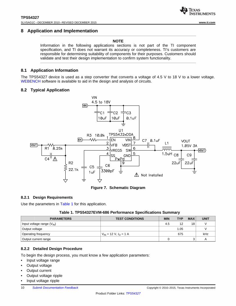
8.1 Application InformationThe TPS54327 device is used as a step converter that converts a voltage of 4.5 V to 18 V to a lower voltage.WEBENCH software is available to aid in the design and analysis of circuits.
8.2 Typical Application
Figure 7. Schematic Diagram
8.2.1 Design RequirementsUse the parameters in Table 1 for this application.
Table 1. TPS54327EVM-686 Performance Specifications SummaryPARAMETERS TEST CONDITIONS MIN TYP MAX UNIT
Input voltage range (VIN) 4.5 12 18 VOutput voltage 1.05 VOperating frequency VIN = 12 V, IO = 1 A 675 kHzOutput current range 0 3 A
8.2.2 Detailed Design ProcedureTo begin the design process, you must know a few application parameters:• Input voltage range• Output voltage• Output current• Output voltage ripple• Input voltage ripple
10 Submit Documentation Feedback Copyright © 2010–2015, Texas Instruments Incorporated
Product Folder Links: TPS54327

2 2=
IPPLo(RMS) O
1+
12I I I
lpp= +
Ipeak O 2
I
I I
V VV IN(max) OUTOUT= xIPP V L x
IN(max) O SW
-I
f
F =P
OUT OUT
1
2 L x Cp
V = 0.765 xOUT
R11 +
R2
æ ö÷ç ÷ç ÷÷çè ø
TPS54327www.ti.com SLVSAG1C –DECEMBER 2010–REVISED DECEMBER 2015
8.2.2.1 Output Voltage Resistors SelectionThe output voltage is set with a resistor divider from the output node to the VFB pin. TI recommends using 1%tolerance or better divider resistors. Start by using Equation 2 to calculate VOUT.
To improve efficiency at very light loads consider using larger value resistors, too high of resistance will be moresusceptible to noise and voltage errors from the VFB input current will be more noticeable.
(2)
8.2.2.2 Output Filter SelectionThe output filter used with the TPS54327 is an LC circuit. This LC filter has double pole at:
(3)
At low frequencies, the overall loop gain is set by the output set-point resistor divider network and the internalgain of the TPS54327. The low-frequency phase is 180 degrees. At the output filter pole frequency, the gain rollsoff at a -40 dB per decade rate and the phase drops rapidly. D-CAP2™ introduces a high-frequency zero thatreduces the gain roll off to -20 dB per decade and increases the phase to 90 degrees one decade above thezero frequency. The inductor and capacitor selected for the output filter must be selected so that the double poleof Equation 3 is located below the high-frequency zero but close enough that the phase boost provided be thehigh-frequency zero provides adequate phase margin for a stable circuit. To meet this requirement use thevalues recommended in Table 2
Table 2. Recommended Component ValuesOUTPUT VOLTAGE (V) R1 (kΩ) R2 (kΩ) C4 (pF) L1 (µH) C8 + C9 (µF)
1 6.81 22.1 1.5 22 to 681.05 8.25 22.1 1.5 22 to 681.2 12.7 22.1 1.5 22 to 681.8 30.1 22.1 5 - 22 2.2 22 to 682.5 49.9 22.1 5 - 22 2.2 22 to 683.3 73.2 22.1 5 - 22 2.2 22 to 685 124 22.1 5 - 22 3.3 22 to 68
6.5 165 22.1 5 - 22 3.3 22 to 68
Because the DC gain is dependent on the output voltage, the required inductor value will increase as the outputvoltage increases. For higher output voltages above 1.8 V, additional phase boost can be achieved by adding afeed forward capacitor (C4) in parallel with R1
The inductor peak-to-peak ripple current, peak current and RMS current are calculated using Equation 4,Equation 5 and Equation 6. The inductor saturation current rating must be greater than the calculated peakcurrent and the RMS or heating current rating must be greater than the calculated RMS current. Use 700 kHz forfSW.
Use 700 kHz for fSW. Make sure the chosen inductor is rated for the peak current of Equation 5 and the RMScurrent of Equation 6.
(4)
(5)
(6)
For this design example, the calculated peak current is 3.47 A and the calculated RMS current is 3.01 A. Theinductor used is a TDK SPM6530-1R5M100 with a peak current rating of 11.5 A and an RMS current rating of11 A.Copyright © 2010–2015, Texas Instruments Incorporated Submit Documentation Feedback 11
Product Folder Links: TPS54327

0 5 10 15 20
V - Input Voltage - VI
1.04
1.05
1.06
1.07
1.08
V-
Ou
tpu
t V
olt
ag
e -
VO
I = 1 AO
I = 0 AO
0 0.5 1 1.5 2 2.5 3
I - Output Current - AO
1.04
1.05
1.06
1.07
1.08
V-
Ou
tpu
t V
olt
ag
e -
VO
V = 12 VIN
V = 18 VIN
V = 5 VIN
INOUT OUT=Co(RMS)
IN O SW
V x (V - V )
12 x V x L xI
f
TPS54327SLVSAG1C –DECEMBER 2010–REVISED DECEMBER 2015 www.ti.com
The capacitor value and ESR determines the amount of output voltage ripple. The TPS54327 is intended for usewith ceramic or other low ESR capacitors. Recommended values range from 22uF to 68uF. Use Equation 7 todetermine the required RMS current rating for the output capacitor.
(7)
For this design two TDK C3216X5R0J226M 22-µF output capacitors are used. The typical ESR is 2 mΩ each.The calculated RMS current is 0.271 A and each output capacitor is rated for 4 A.
8.2.2.3 Input Capacitor SelectionThe TPS54327 requires an input decoupling capacitor and a bulk capacitor is needed depending on theapplication. TI recommends a ceramic capacitor over 10 μF for the decoupling capacitor. TI also recommendsconnecting an additional 0.1-µF capacitor from pin 14 to ground to improve the stability of the overcurrent limitfunction. The capacitor voltage rating must be greater than the maximum input voltage.
8.2.2.4 Bootstrap Capacitor SelectionA 0.1 µF. ceramic capacitor must be connected between the VBST to SW pin for proper operation. TIrecommends using a ceramic capacitor.
8.2.2.5 VREG5 Capacitor SelectionA 1-µF ceramic capacitor must be connected between the VREG5 to GND pin for proper operation. TIrecommends using a ceramic capacitor.
8.2.3 Application Curves
Figure 8. 1.05-V Output Voltage vs Output Current Figure 9. 1.05-V Output Voltage vs Input Voltage
12 Submit Documentation Feedback Copyright © 2010–2015, Texas Instruments Incorporated
Product Folder Links: TPS54327

0.0 0.5 1.0 1.5 2.0 2.5 3.00.0
10.0
20.0
30.0
40.0
50.0
60.0
70.0
80.0
90.0
100.0
VIN = 12 VVIN = 5 V
Output Current (A)
Effi
cien
cy (
%)
0.001 0.01 0.1 1 100.0
10.0
20.0
30.0
40.0
50.0
60.0
70.0
80.0
90.0
100.0
VIN = 12 V
VIN = 5 V
Output Current (A)
Effi
cien
cy (
%)
V (10 mV/div)OV = 1.05 VO
SW (5 V/div)
V = 1.05 VO V (50 mV/div)IN
SW (5 V/div)
EN (10 V/div)
VREG5 (5 V/div)
1 ms/div)
Vout (0.5 V/div)
Vout (50 mV/div)
Iout (2 A/div)
100 s/divm
TPS54327www.ti.com SLVSAG1C –DECEMBER 2010–REVISED DECEMBER 2015
Figure 10. 1.05-V, 0-A to 3-A Load Transient Response Figure 11. Start-Up Wave Form
Figure 12. Voltage Ripple at Output (IO = 3 A) Figure 13. Voltage Ripple at Input (IO = 3 A)
Figure 14. TPS54327EVM-686 Efficiency Figure 15. TPS54327EVM-686 Light Load Efficiency
Copyright © 2010–2015, Texas Instruments Incorporated Submit Documentation Feedback 13
Product Folder Links: TPS54327

TPS54327SLVSAG1C –DECEMBER 2010–REVISED DECEMBER 2015 www.ti.com
9 Power Supply RecommendationsThe TPS54327 device is designed to operate from input supply voltage in the range of 4.5 V to 18 V. Buckconverters require the input voltage to be higher than the output voltage. in this case, the maximumrecommended operating duty cycle is 65%. Using that criteria, the minimum recommended input voltage isVo/0.65.
10 Layout
10.1 Layout Guidelines1. Keep the input switching current loop as small as possible.2. Keep the SW node as physically small and short as possible to minimize parasitic capacitance and
inductance and to minimize radiated emissions. Kelvin connections should be brought from the output to thefeedback pin of the device.
3. Keep analog and non-switching components away from switching components.4. Make a single point connection from the signal ground to power ground.5. Do not allow switching current to flow under the device.6. Keep the pattern lines for VIN and PGND broad.7. Exposed pad of device must be connected to PGND with solder.8. VREG5 capacitor should be placed near the device, and connected PGND.9. Output capacitor should be connected to a broad pattern of the PGND.10. Voltage feedback loop should be as short as possible, and preferably with ground shield.11. Lower resistor of the voltage divider which is connected to the VFB pin should be tied to SGND.12. Providing sufficient via is preferable for VIN, SW and PGND connection.13. PCB pattern for VIN, SW, and PGND should be as broad as possible.14. VIN Capacitor should be placed as near as possible to the device.
14 Submit Documentation Feedback Copyright © 2010–2015, Texas Instruments Incorporated
Product Folder Links: TPS54327

VFB
VREG5
SS GND
EN VIN
VBST
SW
EXPOSEDTHERMAL PADAREA
BOOSTCAPACITOR
VOUT
VIA to Ground Plane
OUTPUTINDUCTOR
OUTPUTFILTERCAPACITOR
SLOWSTARTCAP
ANALOGGROUNDTRACE
VININPUTBYPASSCAPACITOR
VIN
FEEDBACKRESISTORS
TO ENABLECONTROL
POWER GROUND
BIASCAP
Connection toPOWER GROUNDon internal orbottom layer
VINHIGH FREQENCYBYPASSCAPACITOR
TPS54327www.ti.com SLVSAG1C –DECEMBER 2010–REVISED DECEMBER 2015
10.2 Layout Examples
Figure 16. PCB Layout
Copyright © 2010–2015, Texas Instruments Incorporated Submit Documentation Feedback 15
Product Folder Links: TPS54327

VFB
VREG5
SS
GND
EN VIN
VBST
SW
EXPOSEDTHERMAL PADAREA
BOOSTCAPACITOR
VOUT
VIA to Ground Plane
OUTPUTINDUCTOR
OUTPUTFILTERCAPACITOR
SLOWSTARTCAP
ANALOGGROUNDTRACE
VININPUTBYPASSCAPACITOR
VIN
FEEDBACKRESISTORS
TO ENABLECONTROL
POWER GROUND
BIASCAP
Connection toPOWER GROUNDon internal orbottom layer
VINHIGH FREQENCYBYPASSCAPACITOR
VIN
SW
TPS54327SLVSAG1C –DECEMBER 2010–REVISED DECEMBER 2015 www.ti.com
Layout Examples (continued)
Figure 17. PCB Layout for the DRC Package
16 Submit Documentation Feedback Copyright © 2010–2015, Texas Instruments Incorporated
Product Folder Links: TPS54327

TPS54327www.ti.com SLVSAG1C –DECEMBER 2010–REVISED DECEMBER 2015
10.3 Thermal ConsiderationsThis 8-pin DDA package incorporates an exposed thermal pad that is designed to be directly attached to anexternal heatsink. The thermal pad must be soldered directly to the printed-circuit board (PCB). After soldering,the PCB can be used as a heatsink. In addition, through the use of thermal vias, the thermal pad can beattached directly to the appropriate copper plane shown in the electrical schematic for the device, or alternatively,can be attached to a special heatsink structure designed into the PCB. This design optimizes the heat transferfrom the integrated circuit (IC).
For additional information on the exposed thermal pad and how to use the advantage of its heat dissipatingabilities, see the technical brief, PowerPAD™ Thermally Enhanced Package (SLMA002), and the applicationbrief, PowerPAD™ Made Easy (SLMA004).
The exposed thermal pad dimensions for this package are shown in the following illustration.
Figure 18. Thermal Pad Dimensions (Top View)
Copyright © 2010–2015, Texas Instruments Incorporated Submit Documentation Feedback 17
Product Folder Links: TPS54327

TPS54327SLVSAG1C –DECEMBER 2010–REVISED DECEMBER 2015 www.ti.com
11 Device and Documentation Support
11.1 Documentation Support
11.1.1 Related DocumentationFor related documentation see the following:• PowerPAD™ Thermally Enhanced Package, SLMA002• PowerPAD™ Made Easy, SLMA004
11.2 Community ResourcesThe following links connect to TI community resources. Linked contents are provided "AS IS" by the respectivecontributors. They do not constitute TI specifications and do not necessarily reflect TI's views; see TI's Terms ofUse.
TI E2E™ Online Community TI's Engineer-to-Engineer (E2E) Community. Created to foster collaborationamong engineers. At e2e.ti.com, you can ask questions, share knowledge, explore ideas and helpsolve problems with fellow engineers.
Design Support TI's Design Support Quickly find helpful E2E forums along with design support tools andcontact information for technical support.
11.3 TrademarksD-CAP2, E2E are trademarks of Texas Instruments.Blu-ray Disc is a trademark of Blu-ray Disc Association.All other trademarks are the property of their respective owners.
11.4 Electrostatic Discharge CautionThese devices have limited built-in ESD protection. The leads should be shorted together or the device placed in conductive foamduring storage or handling to prevent electrostatic damage to the MOS gates.
11.5 GlossarySLYZ022 — TI Glossary.
This glossary lists and explains terms, acronyms, and definitions.
12 Mechanical, Packaging, and Orderable InformationThe following pages include mechanical, packaging, and orderable information. This information is the mostcurrent data available for the designated devices. This data is subject to change without notice and revision ofthis document. For browser-based versions of this data sheet, refer to the left-hand navigation.
18 Submit Documentation Feedback Copyright © 2010–2015, Texas Instruments Incorporated
Product Folder Links: TPS54327

PACKAGE OPTION ADDENDUM
www.ti.com 1-Mar-2017
Addendum-Page 1
PACKAGING INFORMATION
Orderable Device Status(1)
Package Type PackageDrawing
Pins PackageQty
Eco Plan(2)
Lead/Ball Finish(6)
MSL Peak Temp(3)
Op Temp (°C) Device Marking(4/5)
Samples
TPS54327DDA ACTIVE SO PowerPAD DDA 8 75 Green (RoHS& no Sb/Br)
CU NIPDAU | CU SN Level-2-260C-1 YEAR -40 to 85 54327
TPS54327DDAR ACTIVE SO PowerPAD DDA 8 2500 Green (RoHS& no Sb/Br)
CU NIPDAU | CU SN Level-2-260C-1 YEAR -40 to 85 54327
TPS54327DRCR ACTIVE VSON DRC 10 3000 Green (RoHS& no Sb/Br)
CU NIPDAU Level-2-260C-1 YEAR -40 to 85 54327
TPS54327DRCT ACTIVE VSON DRC 10 250 Green (RoHS& no Sb/Br)
CU NIPDAU Level-2-260C-1 YEAR -40 to 85 54327
(1) The marketing status values are defined as follows:ACTIVE: Product device recommended for new designs.LIFEBUY: TI has announced that the device will be discontinued, and a lifetime-buy period is in effect.NRND: Not recommended for new designs. Device is in production to support existing customers, but TI does not recommend using this part in a new design.PREVIEW: Device has been announced but is not in production. Samples may or may not be available.OBSOLETE: TI has discontinued the production of the device.
(2) Eco Plan - The planned eco-friendly classification: Pb-Free (RoHS), Pb-Free (RoHS Exempt), or Green (RoHS & no Sb/Br) - please check http://www.ti.com/productcontent for the latest availabilityinformation and additional product content details.TBD: The Pb-Free/Green conversion plan has not been defined.Pb-Free (RoHS): TI's terms "Lead-Free" or "Pb-Free" mean semiconductor products that are compatible with the current RoHS requirements for all 6 substances, including the requirement thatlead not exceed 0.1% by weight in homogeneous materials. Where designed to be soldered at high temperatures, TI Pb-Free products are suitable for use in specified lead-free processes.Pb-Free (RoHS Exempt): This component has a RoHS exemption for either 1) lead-based flip-chip solder bumps used between the die and package, or 2) lead-based die adhesive used betweenthe die and leadframe. The component is otherwise considered Pb-Free (RoHS compatible) as defined above.Green (RoHS & no Sb/Br): TI defines "Green" to mean Pb-Free (RoHS compatible), and free of Bromine (Br) and Antimony (Sb) based flame retardants (Br or Sb do not exceed 0.1% by weightin homogeneous material)
(3) MSL, Peak Temp. - The Moisture Sensitivity Level rating according to the JEDEC industry standard classifications, and peak solder temperature.
(4) There may be additional marking, which relates to the logo, the lot trace code information, or the environmental category on the device.
(5) Multiple Device Markings will be inside parentheses. Only one Device Marking contained in parentheses and separated by a "~" will appear on a device. If a line is indented then it is a continuationof the previous line and the two combined represent the entire Device Marking for that device.
(6) Lead/Ball Finish - Orderable Devices may have multiple material finish options. Finish options are separated by a vertical ruled line. Lead/Ball Finish values may wrap to two lines if the finishvalue exceeds the maximum column width.

PACKAGE OPTION ADDENDUM
www.ti.com 1-Mar-2017
Addendum-Page 2
Important Information and Disclaimer:The information provided on this page represents TI's knowledge and belief as of the date that it is provided. TI bases its knowledge and belief on informationprovided by third parties, and makes no representation or warranty as to the accuracy of such information. Efforts are underway to better integrate information from third parties. TI has taken andcontinues to take reasonable steps to provide representative and accurate information but may not have conducted destructive testing or chemical analysis on incoming materials and chemicals.TI and TI suppliers consider certain information to be proprietary, and thus CAS numbers and other limited information may not be available for release.
In no event shall TI's liability arising out of such information exceed the total purchase price of the TI part(s) at issue in this document sold by TI to Customer on an annual basis.

TAPE AND REEL INFORMATION
*All dimensions are nominal
Device PackageType
PackageDrawing
Pins SPQ ReelDiameter
(mm)
ReelWidth
W1 (mm)
A0(mm)
B0(mm)
K0(mm)
P1(mm)
W(mm)
Pin1Quadrant
TPS54327DDAR SOPower PAD
DDA 8 2500 330.0 12.8 6.4 5.2 2.1 8.0 12.0 Q1
TPS54327DRCR VSON DRC 10 3000 330.0 12.4 3.3 3.3 1.1 8.0 12.0 Q2
TPS54327DRCT VSON DRC 10 250 180.0 12.4 3.3 3.3 1.1 8.0 12.0 Q2
PACKAGE MATERIALS INFORMATION
www.ti.com 14-Jan-2016
Pack Materials-Page 1

*All dimensions are nominal
Device Package Type Package Drawing Pins SPQ Length (mm) Width (mm) Height (mm)
TPS54327DDAR SO PowerPAD DDA 8 2500 366.0 364.0 50.0
TPS54327DRCR VSON DRC 10 3000 367.0 367.0 35.0
TPS54327DRCT VSON DRC 10 250 210.0 185.0 35.0
PACKAGE MATERIALS INFORMATION
www.ti.com 14-Jan-2016
Pack Materials-Page 2

GENERIC PACKAGE VIEW
Images above are just a representation of the package family, actual package may vary.Refer to the product data sheet for package details.
DDA 8 PowerPAD TM SOIC - 1.7 mm max heightPLASTIC SMALL OUTLINE
4202561/G


GENERIC PACKAGE VIEW
Images above are just a representation of the package family, actual package may vary.Refer to the product data sheet for package details.
DRC 10 VSON - 1 mm max heightPLASTIC SMALL OUTLINE - NO LEAD
4204102-3/M

www.ti.com
PACKAGE OUTLINE
C
10X 0.300.18
2.4 0.1
2X2
1.65 0.1
8X 0.5
1.00.8
10X 0.50.3
0.050.00
A 3.12.9
B
3.12.9
(0.2) TYP4X (0.25)
2X (0.5)
VSON - 1 mm max heightDRC0010JPLASTIC SMALL OUTLINE - NO LEAD
4218878/B 07/2018
PIN 1 INDEX AREA
SEATING PLANE
0.08 C
1
5 6
10
(OPTIONAL)PIN 1 ID 0.1 C A B
0.05 C
THERMAL PADEXPOSED
SYMM
SYMM11
NOTES: 1. All linear dimensions are in millimeters. Any dimensions in parenthesis are for reference only. Dimensioning and tolerancing per ASME Y14.5M. 2. This drawing is subject to change without notice. 3. The package thermal pad must be soldered to the printed circuit board for optimal thermal and mechanical performance.
SCALE 4.000

www.ti.com
EXAMPLE BOARD LAYOUT
0.07 MINALL AROUND0.07 MAX
ALL AROUND
10X (0.24)
(2.4)
(2.8)
8X (0.5)
(1.65)
( 0.2) VIATYP
(0.575)
(0.95)
10X (0.6)
(R0.05) TYP
(3.4)
(0.25)
(0.5)
VSON - 1 mm max heightDRC0010JPLASTIC SMALL OUTLINE - NO LEAD
4218878/B 07/2018
SYMM
1
5 6
10
LAND PATTERN EXAMPLEEXPOSED METAL SHOWN
SCALE:20X
11SYMM
NOTES: (continued) 4. This package is designed to be soldered to a thermal pad on the board. For more information, see Texas Instruments literature number SLUA271 (www.ti.com/lit/slua271).5. Vias are optional depending on application, refer to device data sheet. If any vias are implemented, refer to their locations shown on this view. It is recommended that vias under paste be filled, plugged or tented.
SOLDER MASKOPENINGSOLDER MASK
METAL UNDER
SOLDER MASKDEFINED
EXPOSED METAL
METALSOLDER MASKOPENING
SOLDER MASK DETAILS
NON SOLDER MASKDEFINED
(PREFERRED)
EXPOSED METAL

www.ti.com
EXAMPLE STENCIL DESIGN
(R0.05) TYP
10X (0.24)
10X (0.6)
2X (1.5)
2X(1.06)
(2.8)
(0.63)
8X (0.5)
(0.5)
4X (0.34)
4X (0.25)
(1.53)
VSON - 1 mm max heightDRC0010JPLASTIC SMALL OUTLINE - NO LEAD
4218878/B 07/2018
NOTES: (continued) 6. Laser cutting apertures with trapezoidal walls and rounded corners may offer better paste release. IPC-7525 may have alternate design recommendations.
SOLDER PASTE EXAMPLEBASED ON 0.125 mm THICK STENCIL
EXPOSED PAD 11:
80% PRINTED SOLDER COVERAGE BY AREASCALE:25X
SYMM
1
56
10
EXPOSED METALTYP11
SYMM

IMPORTANT NOTICE
Texas Instruments Incorporated (TI) reserves the right to make corrections, enhancements, improvements and other changes to itssemiconductor products and services per JESD46, latest issue, and to discontinue any product or service per JESD48, latest issue. Buyersshould obtain the latest relevant information before placing orders and should verify that such information is current and complete.TI’s published terms of sale for semiconductor products (http://www.ti.com/sc/docs/stdterms.htm) apply to the sale of packaged integratedcircuit products that TI has qualified and released to market. Additional terms may apply to the use or sale of other types of TI products andservices.Reproduction of significant portions of TI information in TI data sheets is permissible only if reproduction is without alteration and isaccompanied by all associated warranties, conditions, limitations, and notices. TI is not responsible or liable for such reproduceddocumentation. Information of third parties may be subject to additional restrictions. Resale of TI products or services with statementsdifferent from or beyond the parameters stated by TI for that product or service voids all express and any implied warranties for theassociated TI product or service and is an unfair and deceptive business practice. TI is not responsible or liable for any such statements.Buyers and others who are developing systems that incorporate TI products (collectively, “Designers”) understand and agree that Designersremain responsible for using their independent analysis, evaluation and judgment in designing their applications and that Designers havefull and exclusive responsibility to assure the safety of Designers' applications and compliance of their applications (and of all TI productsused in or for Designers’ applications) with all applicable regulations, laws and other applicable requirements. Designer represents that, withrespect to their applications, Designer has all the necessary expertise to create and implement safeguards that (1) anticipate dangerousconsequences of failures, (2) monitor failures and their consequences, and (3) lessen the likelihood of failures that might cause harm andtake appropriate actions. Designer agrees that prior to using or distributing any applications that include TI products, Designer willthoroughly test such applications and the functionality of such TI products as used in such applications.TI’s provision of technical, application or other design advice, quality characterization, reliability data or other services or information,including, but not limited to, reference designs and materials relating to evaluation modules, (collectively, “TI Resources”) are intended toassist designers who are developing applications that incorporate TI products; by downloading, accessing or using TI Resources in anyway, Designer (individually or, if Designer is acting on behalf of a company, Designer’s company) agrees to use any particular TI Resourcesolely for this purpose and subject to the terms of this Notice.TI’s provision of TI Resources does not expand or otherwise alter TI’s applicable published warranties or warranty disclaimers for TIproducts, and no additional obligations or liabilities arise from TI providing such TI Resources. TI reserves the right to make corrections,enhancements, improvements and other changes to its TI Resources. TI has not conducted any testing other than that specificallydescribed in the published documentation for a particular TI Resource.Designer is authorized to use, copy and modify any individual TI Resource only in connection with the development of applications thatinclude the TI product(s) identified in such TI Resource. NO OTHER LICENSE, EXPRESS OR IMPLIED, BY ESTOPPEL OR OTHERWISETO ANY OTHER TI INTELLECTUAL PROPERTY RIGHT, AND NO LICENSE TO ANY TECHNOLOGY OR INTELLECTUAL PROPERTYRIGHT OF TI OR ANY THIRD PARTY IS GRANTED HEREIN, including but not limited to any patent right, copyright, mask work right, orother intellectual property right relating to any combination, machine, or process in which TI products or services are used. Informationregarding or referencing third-party products or services does not constitute a license to use such products or services, or a warranty orendorsement thereof. Use of TI Resources may require a license from a third party under the patents or other intellectual property of thethird party, or a license from TI under the patents or other intellectual property of TI.TI RESOURCES ARE PROVIDED “AS IS” AND WITH ALL FAULTS. TI DISCLAIMS ALL OTHER WARRANTIES ORREPRESENTATIONS, EXPRESS OR IMPLIED, REGARDING RESOURCES OR USE THEREOF, INCLUDING BUT NOT LIMITED TOACCURACY OR COMPLETENESS, TITLE, ANY EPIDEMIC FAILURE WARRANTY AND ANY IMPLIED WARRANTIES OFMERCHANTABILITY, FITNESS FOR A PARTICULAR PURPOSE, AND NON-INFRINGEMENT OF ANY THIRD PARTY INTELLECTUALPROPERTY RIGHTS. TI SHALL NOT BE LIABLE FOR AND SHALL NOT DEFEND OR INDEMNIFY DESIGNER AGAINST ANY CLAIM,INCLUDING BUT NOT LIMITED TO ANY INFRINGEMENT CLAIM THAT RELATES TO OR IS BASED ON ANY COMBINATION OFPRODUCTS EVEN IF DESCRIBED IN TI RESOURCES OR OTHERWISE. IN NO EVENT SHALL TI BE LIABLE FOR ANY ACTUAL,DIRECT, SPECIAL, COLLATERAL, INDIRECT, PUNITIVE, INCIDENTAL, CONSEQUENTIAL OR EXEMPLARY DAMAGES INCONNECTION WITH OR ARISING OUT OF TI RESOURCES OR USE THEREOF, AND REGARDLESS OF WHETHER TI HAS BEENADVISED OF THE POSSIBILITY OF SUCH DAMAGES.Unless TI has explicitly designated an individual product as meeting the requirements of a particular industry standard (e.g., ISO/TS 16949and ISO 26262), TI is not responsible for any failure to meet such industry standard requirements.Where TI specifically promotes products as facilitating functional safety or as compliant with industry functional safety standards, suchproducts are intended to help enable customers to design and create their own applications that meet applicable functional safety standardsand requirements. Using products in an application does not by itself establish any safety features in the application. Designers mustensure compliance with safety-related requirements and standards applicable to their applications. Designer may not use any TI products inlife-critical medical equipment unless authorized officers of the parties have executed a special contract specifically governing such use.Life-critical medical equipment is medical equipment where failure of such equipment would cause serious bodily injury or death (e.g., lifesupport, pacemakers, defibrillators, heart pumps, neurostimulators, and implantables). Such equipment includes, without limitation, allmedical devices identified by the U.S. Food and Drug Administration as Class III devices and equivalent classifications outside the U.S.TI may expressly designate certain products as completing a particular qualification (e.g., Q100, Military Grade, or Enhanced Product).Designers agree that it has the necessary expertise to select the product with the appropriate qualification designation for their applicationsand that proper product selection is at Designers’ own risk. Designers are solely responsible for compliance with all legal and regulatoryrequirements in connection with such selection.Designer will fully indemnify TI and its representatives against any damages, costs, losses, and/or liabilities arising out of Designer’s non-compliance with the terms and provisions of this Notice.
Mailing Address: Texas Instruments, Post Office Box 655303, Dallas, Texas 75265Copyright © 2018, Texas Instruments Incorporated