Embed Size (px)
Citation preview

AMD Functional Data Sheet,940 Pin Package
31412Publication # 3.05Revision:June 2004Issue Date:

31412 Rev. 3.05 June 2004AMD Functional Data Sheet, 940 Pin Package
Trademarks
AMD, the AMD Arrow logo, AMD Athlon, AMD Opteron and combinations thereof, and 3DNow! are trademarks of Advanced Micro Devices, Inc.
HyperTransport is a licensed trademark of the HyperTransport Technology Consortium.
MMX is a trademark of Intel Corporation.
Other product names used in this publication are for identification purposes only and may be trademarks of their respective companies.
Disclaimer
The contents of this document are provided in connection with Advanced Micro Devices, Inc. (“AMD”) products. AMD makes no rep-resentations or warranties with respect to the accuracy or completeness of the contents of this publication and reserves the right to makechanges to specifications and product descriptions at any time without notice. No license, whether express, implied, arising by estoppelor otherwise, to any intellectual property rights is granted by this publication. Except as set forth in AMD’s Standard Terms and Condi-tions of Sale, AMD assumes no liability whatsoever, and disclaims any express or implied warranty, relating to its products including,but not limited to, the implied warranty of merchantability, fitness for a particular purpose, or infringement of any intellectual propertyright.
AMD’s products are not designed, intended, authorized or warranted for use as components in systems intended for surgical implantinto the body, or in other applications intended to support or sustain life, or in any other application in which the failure of AMD’s prod-uct could create a situation where personal injury, death, or severe property or environmental damage may occur. AMD reserves theright to discontinue or make changes to its products at any time without notice.
© 2002, 2003, 2004 Advanced Micro Devices, Inc. All rights reserved.

31412 Rev 3.05 June 2004 AMD Functional Data Sheet, 940 Pin Package
ContentsRevision History . . . . . . . . . . . . . . . . . . . . . . . . . . . . . . . . . . . . . . . . . . . . . . . . . . . . . . . . . . 8
1 Overview . . . . . . . . . . . . . . . . . . . . . . . . . . . . . . . . . . . . . . . . . . . . . . . . . . . . . . . . . . . . . . . . 9
2 Functional Description . . . . . . . . . . . . . . . . . . . . . . . . . . . . . . . . . . . . . . . . . . . . . . . . . . . . 10
2.1 Instruction Set Support . . . . . . . . . . . . . . . . . . . . . . . . . . . . . . . . . . . . . . . . . . . . . . . . . . 10
2.2 Internal Cache Structures . . . . . . . . . . . . . . . . . . . . . . . . . . . . . . . . . . . . . . . . . . . . . . . . 10
2.2.1 Level 1 Caches . . . . . . . . . . . . . . . . . . . . . . . . . . . . . . . . . . . . . . . . . . . . . . . . . . . . 10
2.2.2 Level 2 Cache . . . . . . . . . . . . . . . . . . . . . . . . . . . . . . . . . . . . . . . . . . . . . . . . . . . . . 10
2.3 Error Handling (Machine Check) . . . . . . . . . . . . . . . . . . . . . . . . . . . . . . . . . . . . . . . . . . 10
2.4 Northbridge . . . . . . . . . . . . . . . . . . . . . . . . . . . . . . . . . . . . . . . . . . . . . . . . . . . . . . . . . . . 11
2.4.1 HyperTransport™ Technology Overview . . . . . . . . . . . . . . . . . . . . . . . . . . . . . . . 11
2.4.1.1 Link Initialization . . . . . . . . . . . . . . . . . . . . . . . . . . . . . . . . . . . . . . . . . . . . . . 12
2.4.1.2 HyperTransport™ Technology Transfer Speeds . . . . . . . . . . . . . . . . . . . . . . 12
2.4.2 Memory Controller . . . . . . . . . . . . . . . . . . . . . . . . . . . . . . . . . . . . . . . . . . . . . . . . . 12
2.4.2.1 Memory Pin Interface . . . . . . . . . . . . . . . . . . . . . . . . . . . . . . . . . . . . . . . . . . 13
2.4.2.2 DRAM Operation . . . . . . . . . . . . . . . . . . . . . . . . . . . . . . . . . . . . . . . . . . . . . . 13
2.4.2.3 DRAM Power Management . . . . . . . . . . . . . . . . . . . . . . . . . . . . . . . . . . . . . . 15
2.4.2.4 Chip Kill (Server/Workstation Products Only) . . . . . . . . . . . . . . . . . . . . . . . 15
2.4.2.5 Main Memory Hardware Scrubbing . . . . . . . . . . . . . . . . . . . . . . . . . . . . . . . 16
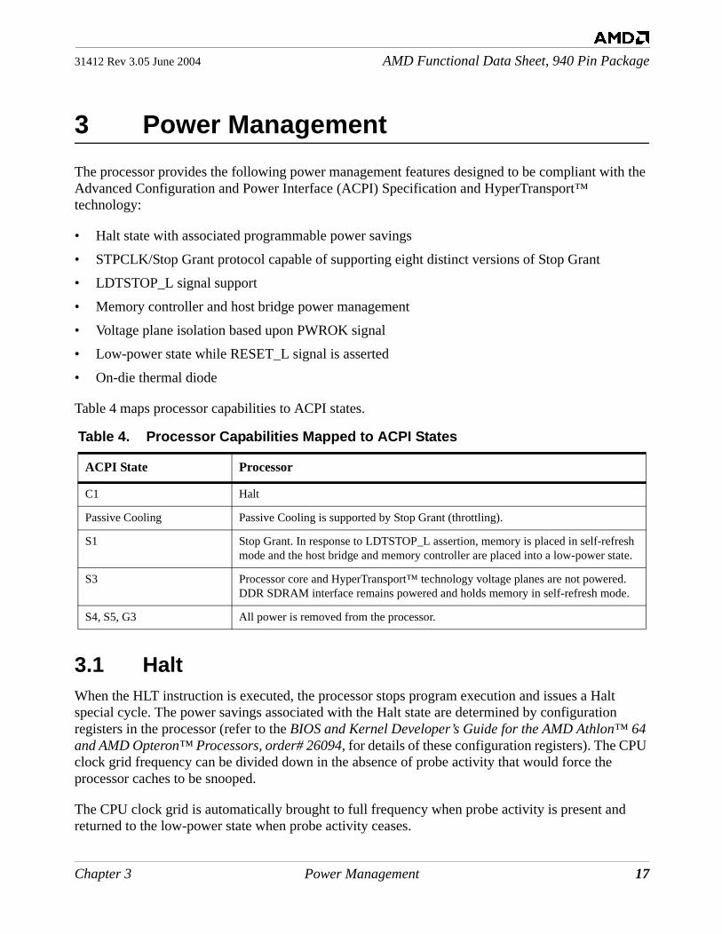
3 Power Management . . . . . . . . . . . . . . . . . . . . . . . . . . . . . . . . . . . . . . . . . . . . . . . . . . . . . . 17
3.1 Halt . . . . . . . . . . . . . . . . . . . . . . . . . . . . . . . . . . . . . . . . . . . . . . . . . . . . . . . . . . . . . . . . . 17
3.2 STPCLK/Stop Grant . . . . . . . . . . . . . . . . . . . . . . . . . . . . . . . . . . . . . . . . . . . . . . . . . . . . 18
3.3 PWROK . . . . . . . . . . . . . . . . . . . . . . . . . . . . . . . . . . . . . . . . . . . . . . . . . . . . . . . . . . . . . 18
3.4 RESET_L and MEMRESET_L . . . . . . . . . . . . . . . . . . . . . . . . . . . . . . . . . . . . . . . . . . . 19
3.5 Thermal Diode . . . . . . . . . . . . . . . . . . . . . . . . . . . . . . . . . . . . . . . . . . . . . . . . . . . . . . . . 19
3.6 THERMTRIP_L . . . . . . . . . . . . . . . . . . . . . . . . . . . . . . . . . . . . . . . . . . . . . . . . . . . . . . . 19
4 Connection Diagrams . . . . . . . . . . . . . . . . . . . . . . . . . . . . . . . . . . . . . . . . . . . . . . . . . . . . . 21
5 Pin Designations . . . . . . . . . . . . . . . . . . . . . . . . . . . . . . . . . . . . . . . . . . . . . . . . . . . . . . . . . 25
6 Pin Descriptions . . . . . . . . . . . . . . . . . . . . . . . . . . . . . . . . . . . . . . . . . . . . . . . . . . . . . . . . . 41
Contents 3

AMD Functional Data Sheet, 940 Pin Package 31412 Rev 3.05 June 2004
6.1 HyperTransport™ Technology Pins . . . . . . . . . . . . . . . . . . . . . . . . . . . . . . . . . . . . . . . . 42
6.2 DDR SDRAM Memory Interface Pins . . . . . . . . . . . . . . . . . . . . . . . . . . . . . . . . . . . . . . 43
6.3 Miscellaneous Pins . . . . . . . . . . . . . . . . . . . . . . . . . . . . . . . . . . . . . . . . . . . . . . . . . . . . . 45
6.4 Pin States at Reset . . . . . . . . . . . . . . . . . . . . . . . . . . . . . . . . . . . . . . . . . . . . . . . . . . . . . . 48
7 Electrical Data . . . . . . . . . . . . . . . . . . . . . . . . . . . . . . . . . . . . . . . . . . . . . . . . . . . . . . . . . . . 49
7.1 Absolute Maximum Ratings . . . . . . . . . . . . . . . . . . . . . . . . . . . . . . . . . . . . . . . . . . . . . . 49
7.2 HyperTransport™ Technology Interface . . . . . . . . . . . . . . . . . . . . . . . . . . . . . . . . . . . . 50
7.2.1 Operating Conditions . . . . . . . . . . . . . . . . . . . . . . . . . . . . . . . . . . . . . . . . . . . . . . . 50
7.2.2 Reference Information . . . . . . . . . . . . . . . . . . . . . . . . . . . . . . . . . . . . . . . . . . . . . . 52
7.3 DDR SDRAM and Miscellaneous Pins . . . . . . . . . . . . . . . . . . . . . . . . . . . . . . . . . . . . . 53
7.3.1 Operating Conditions . . . . . . . . . . . . . . . . . . . . . . . . . . . . . . . . . . . . . . . . . . . . . . . 54
7.3.2 AC Operating Characteristics . . . . . . . . . . . . . . . . . . . . . . . . . . . . . . . . . . . . . . . . . 58
7.4 Clock Pins . . . . . . . . . . . . . . . . . . . . . . . . . . . . . . . . . . . . . . . . . . . . . . . . . . . . . . . . . . . . 65
7.4.1 Operating Conditions . . . . . . . . . . . . . . . . . . . . . . . . . . . . . . . . . . . . . . . . . . . . . . . 65
7.5 Power-Up Signal Sequencing . . . . . . . . . . . . . . . . . . . . . . . . . . . . . . . . . . . . . . . . . . . . . 67
7.6 Reference Information . . . . . . . . . . . . . . . . . . . . . . . . . . . . . . . . . . . . . . . . . . . . . . . . . . 71
7.7 Thermal Diode Specifications . . . . . . . . . . . . . . . . . . . . . . . . . . . . . . . . . . . . . . . . . . . . 73
7.8 Power Supplies . . . . . . . . . . . . . . . . . . . . . . . . . . . . . . . . . . . . . . . . . . . . . . . . . . . . . . . . 75
7.8.1 Operating Conditions . . . . . . . . . . . . . . . . . . . . . . . . . . . . . . . . . . . . . . . . . . . . . . . 75
7.8.2 Thermal Power . . . . . . . . . . . . . . . . . . . . . . . . . . . . . . . . . . . . . . . . . . . . . . . . . . . . 76
7.8.3 Power Supply Relationships . . . . . . . . . . . . . . . . . . . . . . . . . . . . . . . . . . . . . . . . . . 76
7.8.3.1 Sequencing Relationships . . . . . . . . . . . . . . . . . . . . . . . . . . . . . . . . . . . . . . . 76
7.8.3.2 Sequencing Relationships: Signals to Power Supplies (Stress Conditions) . . 78
7.8.3.3 Power Failures . . . . . . . . . . . . . . . . . . . . . . . . . . . . . . . . . . . . . . . . . . . . . . . . 78
7.8.3.4 Power States . . . . . . . . . . . . . . . . . . . . . . . . . . . . . . . . . . . . . . . . . . . . . . . . . . 78
7.8.3.5 Unused Links . . . . . . . . . . . . . . . . . . . . . . . . . . . . . . . . . . . . . . . . . . . . . . . . . 78
8 Package Specifications . . . . . . . . . . . . . . . . . . . . . . . . . . . . . . . . . . . . . . . . . . . . . . . . . . . . 79
8.1 Mechanical Loading for Lidded Parts . . . . . . . . . . . . . . . . . . . . . . . . . . . . . . . . . . . . . . 79
8.2 Package Diagram . . . . . . . . . . . . . . . . . . . . . . . . . . . . . . . . . . . . . . . . . . . . . . . . . . . . . . 80
4 Contents
List of Figures 5
31412 Rev 3.05 June 2004 AMD Functional Data Sheet, 940 Pin Package
List of FiguresFigure 1. Processor Block Diagram . . . . . . . . . . . . . . . . . . . . . . . . . . . . . . . . . . . . . . . . . . . . . . . . 9
Figure 2. 940 Pin Micro PGA—Top View, Left Side . . . . . . . . . . . . . . . . . . . . . . . . . . . . . . . . . 22
Figure 3. 940 Pin Micro PGA—Top View, Right Side . . . . . . . . . . . . . . . . . . . . . . . . . . . . . . . . 23
Figure 4. Slew Rate Measurement Example . . . . . . . . . . . . . . . . . . . . . . . . . . . . . . . . . . . . . . . . 57
Figure 5. MEMCLK Output Skew . . . . . . . . . . . . . . . . . . . . . . . . . . . . . . . . . . . . . . . . . . . . . . . . 60
Figure 6. MEMDQS Timing Parameter . . . . . . . . . . . . . . . . . . . . . . . . . . . . . . . . . . . . . . . . . . . . 60
Figure 7. DSS/tDSH Timing Parameters . . . . . . . . . . . . . . . . . . . . . . . . . . . . . . . . . . . . . . . . . . . 61
Figure 8. tDQSQV/tDQSQIV Timing Parameters . . . . . . . . . . . . . . . . . . . . . . . . . . . . . . . . . . . . 62
Figure 9. MEMADD/CMD to MEMCLK Timing Parameter (Registered DIMMs) . . . . . . . . . . 63
Figure 10. MEMDQS Edge Arrival Relative to DQs. . . . . . . . . . . . . . . . . . . . . . . . . . . . . . . . . . . 64
Figure 11. MEMRESET_L and MEMCKE_LO/UP Sequencing . . . . . . . . . . . . . . . . . . . . . . . . . 68
Figure 12. Power-Up Signal Sequencing . . . . . . . . . . . . . . . . . . . . . . . . . . . . . . . . . . . . . . . . . . . . 70
Figure 13. Sequencing Relationships for Power Supplies . . . . . . . . . . . . . . . . . . . . . . . . . . . . . . . 77
Figure 14. Ceramic Micro Pin Grid Array Package: Top, Side, and Bottom Views . . . . . . . . . . . 80

AMD Functional Data Sheet, 940 Pin Package 31412 Rev 3.05 June 2004
List of TablesTable 1. Product-Specific HyperTransport™ Support . . . . . . . . . . . . . . . . . . . . . . . . . . . . . . . . 11
Table 2. DRAM Interface Speed vs. CPU Core Clock Multiplier . . . . . . . . . . . . . . . . . . . . . . . 14
Table 3. Total Memory Sizes Per Chip Select . . . . . . . . . . . . . . . . . . . . . . . . . . . . . . . . . . . . . . 15
Table 4. Processor Capabilities Mapped to ACPI States . . . . . . . . . . . . . . . . . . . . . . . . . . . . . . 17
Table 5. Pin List by Name. . . . . . . . . . . . . . . . . . . . . . . . . . . . . . . . . . . . . . . . . . . . . . . . . . . . . . 26
Table 6. Pin Description Table Definitions. . . . . . . . . . . . . . . . . . . . . . . . . . . . . . . . . . . . . . . . . 41
Table 7. HyperTransport™ Technology Pin Descriptions . . . . . . . . . . . . . . . . . . . . . . . . . . . . . 42
Table 8. DDR SDRAM Memory Interface Pin Descriptions . . . . . . . . . . . . . . . . . . . . . . . . . . . 43
Table 9. Clock Pin Descriptions . . . . . . . . . . . . . . . . . . . . . . . . . . . . . . . . . . . . . . . . . . . . . . . . . 45
Table 10. Miscellaneous Pin Descriptions . . . . . . . . . . . . . . . . . . . . . . . . . . . . . . . . . . . . . . . . . . 45
Table 11. VID[4:0] Encoding . . . . . . . . . . . . . . . . . . . . . . . . . . . . . . . . . . . . . . . . . . . . . . . . . . . . 46
Table 12. JTAG Pin Descriptions . . . . . . . . . . . . . . . . . . . . . . . . . . . . . . . . . . . . . . . . . . . . . . . . . 46
Table 13. Debug Pin Descriptions . . . . . . . . . . . . . . . . . . . . . . . . . . . . . . . . . . . . . . . . . . . . . . . . 47
Table 14. Reset Pin State . . . . . . . . . . . . . . . . . . . . . . . . . . . . . . . . . . . . . . . . . . . . . . . . . . . . . . . 48
Table 15. Absolute Maximum Ratings . . . . . . . . . . . . . . . . . . . . . . . . . . . . . . . . . . . . . . . . . . . . . 49
Table 16. DC Operating Conditions for HyperTransport™ Technology Interface . . . . . . . . . . . 50
Table 17. AC Operating Conditions for HyperTransport™ Technology Interface . . . . . . . . . . . 51
Table 18. Internal Termination for HyperTransport™ Technology Interface . . . . . . . . . . . . . . . 52
Table 19. DC Operating Conditions . . . . . . . . . . . . . . . . . . . . . . . . . . . . . . . . . . . . . . . . . . . . . . . 54
Table 20. AC Operating Conditions . . . . . . . . . . . . . . . . . . . . . . . . . . . . . . . . . . . . . . . . . . . . . . . 55
Table 21. Input Capacitance . . . . . . . . . . . . . . . . . . . . . . . . . . . . . . . . . . . . . . . . . . . . . . . . . . . . . 55
Table 22. Slew Rate of DDR SDRAM Signals. . . . . . . . . . . . . . . . . . . . . . . . . . . . . . . . . . . . . . . 55
Table 23. Slew Rate of RESET_L, LDTSTOP_L, and PWROK . . . . . . . . . . . . . . . . . . . . . . . . . 56
Table 24. Package Routing Skew . . . . . . . . . . . . . . . . . . . . . . . . . . . . . . . . . . . . . . . . . . . . . . . . . 57
Table 25. Electrical AC Timing Characteristics for DDR SDRAM Signals . . . . . . . . . . . . . . . . 58
Table 26. DC Operating Conditions for CLKIN_H/L and FBCLKOUT_H/L Pins . . . . . . . . . . . 65
Table 27. AC Operating Conditions for CLKIN_H/L and FBCLKOUT_H/L Pins . . . . . . . . . . . 66
Table 28. Metal Mask VID[4:0] Values . . . . . . . . . . . . . . . . . . . . . . . . . . . . . . . . . . . . . . . . . . . . 68
6 List of Tables

31412 Rev 3.05 June 2004 AMD Functional Data Sheet, 940 Pin Package
Table 29. MEMRESET_L and MEMCKE_LO/UP Initialization Timing . . . . . . . . . . . . . . . . . . 68
Table 30. MEMCKE_LO/UP Delay from MEMRESET_L During Exit from Self-Refresh . . . . 69
Table 31. Internal Termination for Miscellaneous Pins Interface. . . . . . . . . . . . . . . . . . . . . . . . . 71
Table 32. External Required Circuits (Pins Not Normally Used in System) . . . . . . . . . . . . . . . . 72
Table 33. Thermal Diode Specification Revision and Frequency Guide . . . . . . . . . . . . . . . . . . . 73
Table 34. Thermal Diode Specifications (Revision and Frequency Dependent, see Table 33) . . 73
Table 35. Thermal Diode Specifications (Revision and Frequency Dependent, see Table 33) . . 74
Table 36. Combined AC and DC Operating Conditions for Power Supplies . . . . . . . . . . . . . . . . 75
Table 37. Sequencing Relationships for Power Supplies . . . . . . . . . . . . . . . . . . . . . . . . . . . . . . . 77
Table 38. Mechanical Loading for Lidded Parts. . . . . . . . . . . . . . . . . . . . . . . . . . . . . . . . . . . . . . 79
List of Tables 7

8 Revision History
AMD Functional Data Sheet, 940 Pin Package 31412 Rev 3.05 June 2004
Revision History
Date Revision Description
June 2004 3.05 New document per new data sheet structuring. Specification modifications from previous document structure include: Added mechanical loading Section 8.1. Thermal diode change to 2 sourcing currents only in section 7.7. Clarified THERMTRIP_L operation in Section 3.6. Added Table 27 to Section 7.5 to enumerate metal mask VID[4:0] encodings for different processor revisions. Clarified DDR400 VDDIO specification in Table 35. Added slew rates for some misc signals in Table 22. Corrected MEMDQS naming in Table 7. Added Table 1 to clarify HyperTransport™ support. Clarified burst length support in Section 2.4.2.

Chapter 1 Overview 9
31412 Rev 3.05 June 2004 AMD Functional Data Sheet, 940 Pin Package
1 Overview
The processor is designed for high-performance applications. It provides up to three high-performance HyperTransport™ links to I/O, as well as a 128-bit high-performance DDR SDRAM memory controller. A block diagram of the processor is shown in Figure 1.
Figure 1. Processor Block Diagram
CPU Core
1-MbyteL2 Cache
Hyp
erTr
ansp
ort
™In
terf
ace
DD
R S
DR
AM
Inte
rfac
e
Northbridge
3 x
16/1
640
0–16
00 M
T/s
128-
bits
DD
R S
DR
AM
100/
133/
166/
200
MH
z16
-bits
EC
C
MEMCLK_LO_H/L[3:0]MEMCKE_UP
MEMRESET_LMEMCS_L[7:0]MEMADD[13:0]MEMBANK[1:0]MEMRAS_LMEMCAS_LMEMWE_LMEMDQS[35:0]MEMDATA[127:0]MEMCHECK[15:0]
MEMZNMEMZPMEMVREF
L0_CLKIN_H/L[1:0]L0_CTLIN_H/L[0]
L0_CADIN_H/L[15:0]
L0_CLKOUT_H/L[1:0]L0_CTLOUT_H/L[0]
L0_CADOUT_H/L[15:0]
LDTSTOP_L
L0_REF0L0_REF1
CLKIN_H/LFBCLKOUT_H/L PLLs
JTAGTDITDO
TCKTMSTRST_LDBREQ_LDBRDY
VDDA
RESET_LPWROK
Control
VID[4:0]
THERMDATHERMDC
THERMTRIP_L
COREFB_H/L
andDebugand
Clocks
64-KbyteL1 I-Cache
64-KbyteL1 D-Cache
MEMCLK_UP_H/L[3:0]
L1_CLKIN_H/L[1:0]L1_CTLIN_H/L[0]
L1_CADIN_H/L[15:0]
L1_CLKOUT_H/L[1:0]L1_CTLOUT_H/L[0]
L1_CADOUT_H/L[15:0]
L2_CLKIN_H/L[1:0]L2_CTLIN_H/L[0]
L2_CADIN_H/L[15:0]
L2_CLKOUT_H/L[1:0]L2_CTLOUT_H/L[0]
L2_CADOUT_H/L[15:0]
MEMCKE_LO
PRESENCE_DET
Links 1 and 2 are available on Server/Workstation products only.

AMD Functional Data Sheet, 940 Pin Package 31412 Rev 3.05 June 2004
2 Functional Description
2.1 Instruction Set SupportThe processor supports the standard x86-instruction set defined in the AMD64 Architecture Programmer’s Manual, volumes 3–5, order# 24594. In addition, the processor supports the following extensions to the standard x86 instruction set, which are described in the same volume set:
• AMD64 instructions
• MMX™ and 3DNow!™ technology instructions
• SSE and SSE2 instructions
2.2 Internal Cache StructuresThe processor implements internal caching structures as described in the following sections.
2.2.1 Level 1 Caches
The L1 data cache (L1 D-Cache) contains 64 Kbytes of storage organized as two-way set associative. The L1 data cache is protected with ECC. Two simultaneous 64-bit operations (load, store, or combination) are supported. The L1 instruction cache (L1 I-Cache) contains 64 Kbytes of storage organized as two-way associative. The L1 instruction cache is protected with parity.
2.2.2 Level 2 Cache
The L2 cache contains both instruction and data stream information. It is organized as 16-way set-associative. The L2 cache data and tag store is protected with ECC. When a given cache line in the L2 cache contains instruction stream information, the ECC bits associated with the given line are used to store predecode and branch prediction information.
2.3 Error Handling (Machine Check)The processor implements the standard x86 machine check architecture as defined in the AMD64 Architecture Programmer’s Manual, Volume 2, order# 24593, and the BIOS and Kernel Developer’s Guide for the AMD Athlon™ 64 and AMD Opteron™ Processors, order# 26094.
10 Functional Description Chapter 2

31412 Rev 3.05 June 2004 AMD Functional Data Sheet, 940 Pin Package
The machine check architecture is defined with ECC single-bit detection/correction and double-bit detection for the following arrays:
• L1 Data Cache Storage
• L2 Data Cache Storage
• L2 Data Cache Tag
• Instruction Cache
• DRAM. See “Memory Controller” on page 12.
2.4 NorthbridgeThe Northbridge logic in the processor refers to the HyperTransport™ technology interface and the memory controller and their respective interfaces to the CPU cores. These interfaces are described in more detail in the following sections.
2.4.1 HyperTransport™ Technology Overview
The processor includes up to three16-bit HyperTransport™ technology interfaces capable of operating up to 1600 mega-transfers per second (MT/s) with a resulting bandwidth of up to 6.4 Gbytes/s (3.2 Gbytes/s in each direction). Refer to Table 1 for product-specific details on HyperTransport™ interfaces. The processor supports HyperTransport™ technology synchronous clocking mode. Refer to the HyperTransport™ I/O Link Specification (www.hypertransport.org) for details of link operation.
Notes:1. Coherency is supported on any one of the three HyperTransport™ interfaces on Server/Workstation DP products.
Table 1.Product-Specific HyperTransport™ Support
Product Number of InterfacesMaximum Number of Coherent Interfaces
Desktop 1 0
Server/Workstation Uni-Processor (UP) 3 0
Server/Workstation Dual-Processor (DP) 3 11
Server/Workstation Multi-Processor (MP) 3 3
Chapter 2 Functional Description 11

AMD Functional Data Sheet, 940 Pin Package 31412 Rev 3.05 June 2004
2.4.1.1 Link Initialization
The HyperTransport™ I/O Link Specification details the negotiation that occurs at power-on to determine the widths and rates used with the link. Refer also to the BIOS and Kernel Developer’s Guide for the AMD Athlon™ 64 and AMD Opteron™ Processors, order# 26094, for information about link initialization and setup of routing tables.
Refer to the AMD Athlon™ 64 FX and AMD Opteron™ Processor Motherboard Design Guide, order# 25180, for details on the proper HyperTransport™ technology signal termination resistor values.
2.4.1.2 HyperTransport™ Technology Transfer Speeds
The HyperTransport™ link of the processor is capable of operating at 400, 800, 1200, and 1600 MT/s. The link transfer rate is determined during the software configuration of the system, as specified in the HyperTransport™ I/O Link Specification.
2.4.2 Memory Controller
The processor’s memory controller provides a programmable interface to a variety of standard registered DDR SDRAM DIMM configurations. Refer to the BIOS and Kernel Developer’s Guide for the AMD Athlon™ 64 and AMD Opteron™ Processors, order# 26094, for supported DRAM speeds under specific loading conditions.
• Self-Refresh mode
• The controller provides programmable control of DRAM timing parameters to support the following memory speeds:
— 100 MHz (DDR200) PC-1600 DIMMs
— 133 MHz (DDR266) PC-2100 DIMMs
— 166 MHz (DDR333) PC-2700 DIMMs
— 200 MHz (DDR400) PC-3200 DIMMs*
• DRAM devices that are 4, 8 and 16 bits wide
• DIMM sizes from 32 Mbytes (using 64Mb x16 DRAMs) to 4 Gbytes (using a stacked DIMM with 1Gb x4 DRAMs)
• Interleaving memory within DIMMs
• Stacked registered DIMMs
• ECC checking with single-bit correction and double-bit detection
• Chip Kill ECC allows single symbol correction and double symbol detection (Server/Workstation products only)
• May be configured for 32-byte or 64-byte burst length (32-byte mode applies only when operat-
12 Functional Description Chapter 2

31412 Rev 3.05 June 2004 AMD Functional Data Sheet, 940 Pin Package
ing with a 64-bit DRAM interface).
• Programmable page-policy:
— Supports up to 16 open pages total across all chip-selects
— Statically idle open-page time
— Optional dynamic precharge control based on page-hit/miss history
* DDR400 supported by Rev C0 and later, Refer to AMD Opteron™ Processor Power and Thermal Data Sheet, order# 30417, for silicon revision determination
For programming information and specific details of the features listed above, refer to the BIOS and Kernel Developer’s Guide for the AMD Athlon™ 64 and AMD Opteron™ Processors, order# 26094.
2.4.2.1 Memory Pin Interface
The memory controller of the processor supports registered DDR SDRAM DIMMs. The following list applies to the pin interface:
• The MEMRESET_L pin is required for registered DIMMs and is used to reset the register as required to support the Suspend to RAM power management state (ACPI S3).
• The memory controller can be configured to support either 64-bit or 128-bit memory interfaces. Refer to the BIOS and Kernel Developer’s Guide for the AMD Athlon™ 64 and AMD Opteron™ Processors, order# 26094, for restrictions based on DDR SDRAM speed.
• A 64-bit memory system can support up to four DIMMs, each 64-bits wide
• A 128-bit memory system can support up to eight DIMMs, each 64-bits wide, and must bepopulated in even numbered pairs as described in the AMD Athlon™ 64 FX and AMDOpteron™ Processor Motherboard Design Guide, order# 25180.
• Registered DIMMs configured with x4 DRAMs require an additional 16 DQS pins without ECC support or 18 DQS pins with ECC support. The processor’s memory controller provides a total of 36 DQS pins to accommodate this requirement. The additional DQS pins can be connected to the DIMM Data Mask (DM) pins when connected to x8 or x16 DIMMs. DIMMs populated with x4 devices normally connect the DRAM Data Mask (DM) pins to VSS.
2.4.2.2 DRAM Operation
At power-on reset, the MEMCKE_LO/UP and MEMRESET_L pins are driven Low while the processor PLLs are ramping. Clocks are driven on the MEMCLK_LO_H/L[3:0] and MEMCLK_UP_H/L[3:0] pins only after BIOS programs the appropriate clock ratio value in the memory controller configuration registers. The actual DRAM frequency may vary for some speeds based on the CPU clock multiplier, as shown in Table 2 on page 14 (the memory controller automatically adjusts refresh counters at all speeds as required to meet the device refresh specifications). Refer to “Power-Up Signal Sequencing” on page 67 for further details on the sequencing of the MEMRESET_L and MEMCKE_LO/UP pins.
Chapter 2 Functional Description 13

AMD Functional Data Sheet, 940 Pin Package 31412 Rev 3.05 June 2004
Table 2. DRAM Interface Speed vs. CPU Core Clock Multiplier
Notes:1. DDR400 (200MHz) supported by Rev C0 and later. Refer to the AMD Opteron™ Processor Power and Thermal
Data Sheet, order# 30417 for silicon revision determination.
Table 3 on page 15 lists the maximum memory sizes per chip-select for the various supported DRAM device configurations. Note that for DIMMs using two chip-selects, the total memory size per DIMM is doubled. Refer to the AMD Athlon™ 64 FX and AMD Opteron™ Processor Motherboard Design Guide, order# 25180, for details on the connection scheme for registered DIMMs.
MultiplierCore
Frequency
DRAM Frequency
100 MHz 133 MHz 166 MHz 200 MHz1
4 800 MHz 100.00 133.33 160.00 160.00
5 1000 MHz 100.00 125.00 166.66 200.00
6 1200 MHz 100.00 133.33 150.00 200.00
7 1400 MHz 100.00 127.27 155.55 200.00
8 1600 MHz 100.00 133.33 160.00 200.00
9 1800 MHz 100.00 128.57 163.63 200.00
10 2000 MHz 100.00 133.33 166.66 200.00
11 2200 MHz 100.00 129.41 157.14 200.00
12 2400 MHz 100.00 133.33 160.00 200.00
13 2600 MHz 100.00 130.00 162.50 200.00
14 Functional Description Chapter 2

31412 Rev 3.05 June 2004 AMD Functional Data Sheet, 940 Pin Package
Table 3. Total Memory Sizes Per Chip Select
The controller supports programmable timing and refresh as described in the BIOS and Kernel Developer’s Guide for the AMD Athlon™ 64 and AMD Opteron™ Processors, order# 26094. Auto-refresh is supported and is staggered by tRFC across chip-selects to reduce system noise. Unpopulated DIMM slots are not refreshed.
2.4.2.3 DRAM Power Management
The memory controller supports self-refresh mode to accommodate various power management states such as ACPI S1 and S3 states. The MEMRESET_L pin is provided for resetting the registers on registered DDR SDRAM DIMMs as required for the S3 (Suspend-to-RAM) power management state.
2.4.2.4 Chip Kill (Server/Workstation Products Only)
In Chip Kill mode the memory controller can correct single symbol errors and detect double symbol errors across the 128-bit wide data path. This feature optionally takes the place of normal ECC error detection and correction. Operating the memory controller with Chip Kill enabled will result in a two
Devices Used on DIMMs Size Per CS
64 M-bit (4M x4-bits x4 banks) 128 Mbyte
64 M-bit (2M x8-bits x4 banks) 64 Mbyte
64 M-bit (1M x16-bits x4 banks) 32 Mbyte
128 M-bit (8M x4-bits x4 banks) 256 Mbyte
128 M-bit (4M x8-bits x4 banks) 128 Mbyte
128 M-bit (2M x16-bits x4 banks) 64 Mbyte
256 M-bit (16M x4-bits x4 banks) 512 Mbyte
256 M-bit (8M x8-bits x4 banks) 256 Mbyte
256 M-bit (4M x16-bits x4 banks) 128 Mbyte
512 M-bit (32M x4-bits x4 banks) 1 Gbyte
512 M-bit (16M x8-bits x4 banks) 512 Mbyte
512 M-bit (8M x16-bits x4 banks) 256 Mbyte
1 G-bit (64M x4-bits x4 banks) 2 Gbyte
1 G-bit (32M x8-bits x4 banks) 1 Gbyte
1 G-bit (16M x16-bits x4 banks) 512 Mbyte
Chapter 2 Functional Description 15

AMD Functional Data Sheet, 940 Pin Package 31412 Rev 3.05 June 2004
clock latency penalty on memory access due to the detection, correction, and data containment overhead of operating in this mode.
2.4.2.5 Main Memory Hardware Scrubbing
The memory controller scrubs the main memory arrays to prevent the build up of soft errors. Any correctable or non-correctable errors are logged to the machine check logs and non-correctable errors can be programmed to invoke the machine check interrupt. A correctable error is a single-bit error in normal ECC mode or a single symbol error in Chip Kill mode (Server/Workstation products only). There are two modes of main memory scrubbing that can be used independently or combined, as described in the following sections.
2.4.2.5.1 Sequential Scrubbing
In this mode, the scrubber sequentially proceeds through main memory, performing a read-write cycle or a read-modify-write cycle if a correctable error is found. The scrubber scrubs one cache line on each scrub interval that is programmable from 40 ns to 84 ms.
2.4.2.5.2 Source Correction Scrubbing
In this mode, the scrubber is directed to scrub any cache line that is the source of any corrected error during normal accesses. During normal operation when source correction scrubbing is disabled, single-bit errors are corrected on the fly and the corrected data is passed without updating the source memory location. When source scrubbing is enabled the scrubber also corrects the source memory location.
2.4.2.5.3 Sequential Plus Source Correction Scrubbing
When both sequential and source correction scrubbing are enabled, the scrubber sequentially proceeds through main memory. If a correctable error is detected during normal operation, the scrubber is redirected to the location of the error, and after it corrects that location in main memory it resumes sequential scrubbing at the previous location.
16 Functional Description Chapter 2
31412 Rev 3.05 June 2004 AMD Functional Data Sheet, 940 Pin Package
3 Power Management
The processor provides the following power management features designed to be compliant with the Advanced Configuration and Power Interface (ACPI) Specification and HyperTransport™ technology:
• Halt state with associated programmable power savings
• STPCLK/Stop Grant protocol capable of supporting eight distinct versions of Stop Grant
• LDTSTOP_L signal support
• Memory controller and host bridge power management
• Voltage plane isolation based upon PWROK signal
• Low-power state while RESET_L signal is asserted
• On-die thermal diode
Table 4 maps processor capabilities to ACPI states.
3.1 HaltWhen the HLT instruction is executed, the processor stops program execution and issues a Halt special cycle. The power savings associated with the Halt state are determined by configuration registers in the processor (refer to the BIOS and Kernel Developer’s Guide for the AMD Athlon™ 64 and AMD Opteron™ Processors, order# 26094, for details of these configuration registers). The CPU clock grid frequency can be divided down in the absence of probe activity that would force the processor caches to be snooped.
The CPU clock grid is automatically brought to full frequency when probe activity is present and returned to the low-power state when probe activity ceases.
Table 4. Processor Capabilities Mapped to ACPI States
ACPI State Processor
C1 Halt
Passive Cooling Passive Cooling is supported by Stop Grant (throttling).
S1 Stop Grant. In response to LDTSTOP_L assertion, memory is placed in self-refresh mode and the host bridge and memory controller are placed into a low-power state.
S3 Processor core and HyperTransport™ technology voltage planes are not powered. DDR SDRAM interface remains powered and holds memory in self-refresh mode.
S4, S5, G3 All power is removed from the processor.
Chapter 3 Power Management 17

AMD Functional Data Sheet, 940 Pin Package 31412 Rev 3.05 June 2004
If a STPCLK assertion message is received while the processor is in the Halt state, the processor enters the Stop Grant state and issues a Stop Grant special cycle. When a STPCLK deassertion message is received, the processor exits the Stop Grant state and returns to the Halt state.
The processor exits the Halt state in response to PWROK deassertion, RESET_L assertion, INIT, NMI, SMI, or any unmasked interrupt received over the HyperTransport™ link.
3.2 STPCLK/Stop GrantWhen the processor recognizes the STPCLK assertion message, it enters the Stop Grant state on the next instruction boundary and issues a Stop Grant special cycle. The power savings associated with the Stop Grant state are determined by configuration registers in the processor. The power savings mechanisms associated with the Stop Grant state include the following:
• CPU clock grid divisor applied in the absence of probe activity. If probe activity that requires a cache snoop occurs while the processor is in the Stop Grant state, the clock grid is ramped back up to service the probe. When probe activity ceases, the CPU clock grid is ramped back down again.
• Placing system memory into self-refresh mode in response to LDTSTOP_L signal assertion.
• Ramping the processor host bridge/memory controller clock grid down in response to LDTSTOP_L signal assertion.
• Changing HyperTransport™ link width and/or link frequency in response to LDTSTOP_L signal assertion.
The processor exits the Stop Grant state when it receives the following:
• A STPCLK deassertion message.
• RESET_L pin asserted or an INIT assertion message.
• PWROK is deasserted.
If the LDTSTOP_L signal is asserted after the processor is in the Stop Grant state, then LDTSTOP_L must be deasserted, and the HyperTransport™ link must be re-initialized before a STPCLK deassertion message can be received by the processor to bring the processor out of the Stop Grant state.
The processor’s host bridge ensures that STPCLK messages are passed to the CPU prior to the subsequent I/O response to the cycle that caused STPCLK assertion as long as the subsequent I/O response message has the PassPW bit clear and the Unit ID of the response matches the Unit ID of the STPCLK message.
3.3 PWROKWhen PWROK is deasserted, the processor performs the following steps:
18 Power Management Chapter 3

31412 Rev 3.05 June 2004 AMD Functional Data Sheet, 940 Pin Package
• Isolates its VDDIO- and VTT-powered logic from all other internal logic to prevent leakage current paths between power planes.
• Tristates all DDR SDRAM I/O pins except for the MEMCKE_LO/UP and MEMRESET_L out-puts, which are driven Low.
• Drives its VID[4:0] outputs to the value that selects the startup core voltage level.
3.4 RESET_L and MEMRESET_LWhen RESET_L is asserted, the processor performs the following steps:
• The processor core is held in a low-power state.
• The MEMCKE_LO/UP and MEMRESET_L outputs are forced low.
After RESET_L is deasserted, BIOS must program the appropriate clock divisor in the memory con-troller configuration registers, causing the MEMCLK_LO_H/L[3:0] and MEMCLK_UP_H/L[3:0] clocks to be driven. Refer to “Power-Up Signal Sequencing” on page 67 for details of RESET_L and MEMRESET_L sequencing during initial power-on.
3.5 Thermal DiodeThe processor provides an on-die thermal diode with anode and cathode brought out to processor pins. This diode can be read by an external temperature sensor to determine the processor’s temperature. Refer to the AMD Athlon™ 64 FX and AMD Opteron™ Processor Motherboard Design Guide, order# 25180, for details on connecting the thermal diode.
3.6 THERMTRIP_LThe processor provides a hardware-enforced thermal protection mechanism. When the processor’s die temperature exceeds a specified temperature, the processor is designed to stop its internal clocks and asserting the THERMTRIP_L output.
THERMTRIP_L assertion is only valid when PWROK is asserted and RESET_L is deasserted.
THERMTRIP_L assertion indicates the processor die temperature has exceeded normal operating parameters. PWROK must be deasserted in response to a THERMTRIP_L assertion to help ensure proper processor operation.
Once asserted THERMTRIP_L remains asserted until RESET_L is asserted.
If the processor’s die temperature still exceeds the thermal trip point when RESET_L is deasserted, THERMTRIP_L will immediately be reasserted and the processor’s internal clocks will be stopped.
Chapter 3 Power Management 19

AMD Functional Data Sheet, 940 Pin Package 31412 Rev 3.05 June 2004
20 Power Management Chapter 3

31412 Rev 3.05 June 2004 AMD Functional Data Sheet, 940 Pin Package
4 Connection Diagrams
The pinout for the AMD Opteron™ processor is illustrated in this chapter. The ball map is divided into two parts. Figure 2 on page 22 shows the left portion of the top view, and Figure 3 on page 23 shows the right portion of the top view.
The pin designations are defined in Chapter 5. Table 5 on page 26 lists the pins alphabetically by pin name.
Chapter 4 Connection Diagrams 21

AMD Functional Data Sheet, 940 Pin Package 31412 Rev 3.05 June 2004
Notes:1. Links 1 and 2 are available on Server/Workstation products only. See Table 5 on page 26 for proper no connect
(NC_*) naming for Desktop products.2. PRESENCE_DET is used for Server/Workstation products only. This pin should be connected to VSS for Desktop
products. See the AMD Athlon™ 64 FX and AMD Opteron™ Processor Motherboard Design Guide, order# 25180, for connection details.
3. VLDT is referenced as a unified plane for Desktop products. See Table 5 on page 26 for proper VLDT pin naming for Desktop products.
Figure 2. 940 Pin Micro PGA—Top View, Left Side
1 2 3 4 5 6 7 8 9 10 11 12 13 14 15
A L1_CADOUT_H[0]1 L1_CADOUT_L[0]1 L1_CADOUT_H[2]1 L1_CADOUT_L[2]1 L1_CLKOUT_H[0]1 L1_CLKOUT_L[0]1 L1_CADOUT_H[5]1 L1_CADOUT_L[5]1 L1_CADOUT_H[7]1 L1_CADOUT_L[7]1 L1_CTLIN_L[0]1 L1_CTLIN_H[0]1 L1_CADIN_L[6]1
B VSS L1_CADOUT_H[1]1 VDD L1_CADOUT_H[3]1 VSS L1_CADOUT_H[4]1 VDD L1_CADOUT_H[6]1 VSS L1_CTLOUT_H[0]1 VDD L1_CADIN_L[7]1 VSS
C VDDA1 VDDA3 L1_CADOUT_L[8]1 L1_CADOUT_L[1]1 L1_CADOUT_L[10]1 L1_CADOUT_L[3]1 L1_CLKOUT_L[1]1 L1_CADOUT_L[4]1 L1_CADOUT_L[13]1 L1_CADOUT_L[6]1 L1_CADOUT_L[15]1 L1_CTLOUT_L[0]1 NC_C13 L1_CADIN_H[7]1 L1_CADIN_H[14]1
D L0_REF0 VDDA2 L1_CADOUT_H[8]1 VDD L1_CADOUT_H[10]1 VSS L1_CLKOUT_H[1]1 VDD L1_CADOUT_H[13]1 VSS L1_CADOUT_H[15]1 VDD NC_D13 VSS L1_CADIN_L[14]1
E L0_REF1 VSS L1_CADOUT_H[9]1 L1_CADOUT_L[9]1 L1_CADOUT_H[11]1 L1_CADOUT_L[11]1 L1_CADOUT_H[12]1 L1_CADOUT_L[12]1 L1_CADOUT_H[14]1 L1_CADOUT_L[14]1 NC_E11 NC_E12 L1_CADIN_L[15]1 L1_CADIN_H[15]1 L1_CADIN_L[13]1
F VSS VSS VSS VDD NC_F7 VSS VID[3] VSS VDD PWROK VSS VSS VDD
G L0_CADIN_H[1] L0_CADIN_L[0] L0_CADIN_H[0] VSS L0_CADIN_H[8] NC_G6 VDD DBRDY VID[4] VID[2] VID[0] RESET_L VSS NC_G14 VSS
H L0_CADIN_L[1] VDD L0_CADIN_H[9] L0_CADIN_L[9] L0_CADIN_L[8] VSS NC_H7 VLDT_13 NC_H9 VLDT_13 VID[1] NC_H12 NC_H13 NC_H14 VSS
J L0_CADIN_H[3] L0_CADIN_L[2] L0_CADIN_H[2] VDD L0_CADIN_H[10] LDTSTOP_L DBREQ_L VSS VLDT_13 VSS VLDT_13 VSS VDD VSS VLDT_13
K L0_CADIN_L[3] VSS L0_CADIN_H[11] L0_CADIN_L[11] L0_CADIN_L[10] VDD CORESENSE_H NC_K8 VSS VLDT_13 VSS VDD VSS VLDT_13 VSS
L L0_CADIN_H[4] L0_CLKIN_L[0] L0_CLKIN_H[0] VSS L0_CLKIN_H[1] COREFB_L COREFB_H NC_L8 VDD VSS VDD VSS VDD VSS VDD
M L0_CADIN_L[4] VDD L0_CADIN_H[12] L0_CADIN_L[12] L0_CLKIN_L[1] VSS VSS VLDT_03 VSS VDD VSS VDD VSS VDD VSS
N L0_CADIN_H[6] L0_CADIN_L[5] L0_CADIN_H[5] VDD L0_CADIN_H[13] NC_N6 VLDT_03 VSS VDD VSS VDD VSS VDD VSS VDD
P L0_CADIN_L[6] VSS L0_CADIN_H[14] L0_CADIN_L[14] L0_CADIN_L[13] VDD VSS VLDT_03 VSS VDD VSS VDD VSS VDD VSS
R L0_CTLIN_H[0] L0_CADIN_L[7] L0_CADIN_H[7] VSS L0_CADIN_H[15] NC_R6 VLDT_03 VSS VDD VSS VDD VSS VDD VSS VDD
T L0_CTLIN_L[0] VDD NC_T3 NC_T4 L0_CADIN_L[15] VSS NC_T7 VDD VSS VDD VSS VDD VSS VDD VSS
U L0_CADOUT_L[7] L0_CTLOUT_H[0] L0_CTLOUT_L[0] VDD NC_U5 NC_U6 VLDT_03 VSS VDD VSS VDD VSS VDD VSS VDD
V L0_CADOUT_H[7] VSS L0_CADOUT_L[15] L0_CADOUT_H[15] NC_V5 VDD VSS VLDT_03 VSS VDD VSS VDD VSS VDD VSS
W L0_CADOUT_L[5] L0_CADOUT_H[6] L0_CADOUT_L[6] VSS L0_CADOUT_L[14] NC_W6 VLDT_03 VSS VDD VSS VDD VSS VDD VSS VDD
Y L0_CADOUT_H[5] VDD L0_CADOUT_L[13] L0_CADOUT_H[13] L0_CADOUT_H[14] VSS VSS VLDT_03 VSS VDD VSS VDD VSS VDD VSS
AA L0_CLKOUT_L[0] L0_CADOUT_H[4] L0_CADOUT_L[4] VDD L0_CADOUT_L[12] NC_AA6 VLDT_03 VSS VDD VSS VDD VSS VDD VSS VDD
AB L0_CLKOUT_H[0] VSS L0_CLKOUT_L[1] L0_CLKOUT_H[1] L0_CADOUT_H[12] VDD VSS VDD VSS VLDT_23 VSS VDD VSS VLDT_23 VSS
AC L0_CADOUT_L[2] L0_CADOUT_H[3] L0_CADOUT_L[3] VSS L0_CADOUT_L[11] NC_AC6 VLDT_23 VSS VLDT_23 VSS VDD VSS VLDT_23
AD L0_CADOUT_H[2] VDD L0_CADOUT_L[10] L0_CADOUT_H[10] L0_CADOUT_H[11] VSS TRST_L VLDT_23 VSS VLDT_23 VSS VDD VSS VDD VSS
AE L0_CADOUT_L[0] L0_CADOUT_H[1] L0_CADOUT_L[1] VDD L0_CADOUT_L[9] TMS TCK TDO NC_AE9 NC_AE10 NC_AE11 NC_AE12 NC_AE13 NC_AE14 THERMTRIP_L
AF L0_CADOUT_H[0] VSS L0_CADOUT_L[8] L0_CADOUT_H[8] L0_CADOUT_H[9] VDD TDI VSS NC_AF9 VDD NC_AF11 VSS NC_AF13 VDD NC_AF15
AG NC_AG1 VSS L2_CADIN_H[8]1 L2_CADIN_L[8]1 L2_CADIN_H[10]1 L2_CADIN_L[10]1 L2_CLKIN_H[1]1 L2_CLKIN_L[1]1 L2_CADIN_H[13]1 L2_CADIN_L[13]1 L2_CADIN_H[15]1 L2_CADIN_L[15]1 NC_AG13 NC_AG14 L2_CADOUT_L[14]1
AH THERMDC NC_AH2 VSS L2_CADIN_L[9]1 VDD L2_CADIN_L[11]1 VSS L2_CADIN_L[12]1 VDD L2_CADIN_L[14]1 VSS NC_AH12 VDD L2_CADOUT_H[15]1 VSS
AJ THERMDA NC_AJ2 L2_CADIN_H[0]1 L2_CADIN_H[9]1 L2_CADIN_H[2]1 L2_CADIN_H[11]1 L2_CLKIN_H[0]1 L2_CADIN_H[12]1 L2_CADIN_H[5]1 L2_CADIN_H[14]1 L2_CADIN_H[7]1 NC_AJ12 L2_CTLOUT_L[0]1 L2_CADOUT_L[15]1 L2_CADOUT_L[6]1
AK PRESENCE_DET2 L2_CADIN_L[0]1 VDD L2_CADIN_L[2]1 VSS L2_CLKIN_L[0]1 VDD L2_CADIN_L[5]1 VSS L2_CADIN_L[7]1 VDD L2_CTLOUT_H[0]1 VSS L2_CADOUT_H[6]1
AL L2_CADIN_H[1]1 L2_CADIN_L[1]1 L2_CADIN_H[3]1 L2_CADIN_L[3]1 L2_CADIN_H[4]1 L2_CADIN_L[4]1 L2_CADIN_H[6]1 L2_CADIN_L[6]1 L2_CTLIN_H[0]1 L2_CTLIN_L[0]1 L2_CADOUT_L[7]1 L2_CADOUT_H[7]1 L2_CADOUT_L[5]1
1 2 3 4 5 6 7 8 9 10 11 12 13 14 15
22 Connection Diagrams Chapter 4

31412 Rev 3.05 June 2004 AMD Functional Data Sheet, 940 Pin Package
Notes:1. Links 1 and 2 are available on Server/Workstation products only. See Table 5 on page 26 for proper no connect
(NC_*) naming for Desktop products.2. VLDT is referenced as a unified plane for Desktop products. See Table 5 on page 26 for proper VLDT pin naming for
Desktop products.
Figure 3. 940 Pin Micro PGA—Top View, Right Side
16 17 18 19 20 21 22 23 24 25 26 27 28 29 30 31
L1_CADIN_H[6]1 L1_CADIN_L[4]1 L1_CADIN_H[4]1 L1_CADIN_L[3]1 L1_CADIN_H[3]1 L1_CADIN_L[1]1 L1_CADIN_H[1]1 VDDIO MEMDATA[4] MEMDATA[1] MEMDATA[6] MEMDATA[2] MEMDATA[3] MEMDATA[9] A
L1_CADIN_L[5]1 VDD L1_CLKIN_L[0]1 VSS L1_CADIN_L[2]1 VDD L1_CADIN_L[0]1 VSS MEMDATA[0] MEMDQS[9] VSS MEMDATA[7] MEMDATA[8] VSS MEMDATA[13] B
L1_CADIN_H[5]1 L1_CADIN_H[12]1 L1_CLKIN_H[0]1 L1_CADIN_H[11]1 L1_CADIN_H[2]1 L1_CADIN_H[9]1 L1_CADIN_H[0]1 VDDIO MEMDATA[5] MEMDQS[0] MEMDATA[71] MEMDATA[72] MEMDATA[12] MEMDQS[1] MEMDQS[10] MEMDATA[14] C
VDD L1_CADIN_L[12]1 VSS L1_CADIN_L[11]1 VDD L1_CADIN_L[9]1 VSS VSS MEMDATA[69] MEMDQS[18] VDDIO MEMDATA[76] VDDIO MEMDATA[77] VSS MEMDATA[15] D
L1_CADIN_H[13]1 L1_CLKIN_L[1]1 L1_CLKIN_H[1]1 L1_CADIN_L[10]1 L1_CADIN_H[10]1 L1_CADIN_L[8]1 L1_CADIN_H[8]1 VDDIO MEMDATA[65] MEMDATA[70] MEMDATA[67] MEMDATA[73] MEMDQS[19] MEMDQS[28] MEMDATA[10] MEMDATA[11] E
VSS VSS VDD VDD VTT VTT MEMVREF0 MEMDATA[68] MEMDQS[27] MEMDATA[66] MEMDATA[78] MEMDATA[79] MEMDATA[74] MEMDATA[20] MEMDATA[16] MEMDATA[17] F
CLKIN_H VSS FBCLKOUT_H VTT MEMCLK_UP_H[3] MEMCLK_UP_L[3] VSS MEMDATA[64] VSS MEMRESET_L VDDIO MEMDATA[75] VDDIO MEMDATA[84] VSS MEMDATA[21] G
CLKIN_L VSS FBCLKOUT_L VTT VDDIO MEMCLK_LO_H[3] MEMCKE_UP MEMCKE_LO MEMDATA[80] MEMDATA[81] MEMDATA[85] MEMDQS[2] MEMDQS[11] MEMDATA[18] H
VLDT_12 VSS VSS VTT VSS VDDIO VSS MEMCLK_LO_L[3] MEMADD[12] MEMADD[11] MEMDQS[20] MEMDQS[29] MEMDATA[82] MEMDATA[22] MEMDATA[23] MEMDATA[19] J
VLDT_12 VSS VDD VSS VDDIO VSS VDDIO MEMADD[9] VSS MEMADD[7] VDDIO MEMDATA[86] VDDIO MEMDATA[87] VSS MEMDATA[24] K
VSS VDD VSS VDDIO VSS VDDIO VSS MEMADD[8] MEMCLK_UP_H[1] MEMCLK_UP_L[1] MEMDATA[83] MEMDATA[88] MEMDATA[92] MEMDATA[28] MEMDATA[29] MEMDATA[25] L
VDD VSS VDD VSS VDD VSS VDDIO NC_M23 MEMADD[5] MEMADD[6] MEMDATA[93] MEMDATA[89] MEMDQS[21] MEMDQS[3] MEMDQS[12] MEMDATA[30] M
VSS VDD VSS VDD VSS VDDIO VSS MEMADD[3] VSS MEMADD[4] VDDIO MEMDQS[30] VDDIO MEMDATA[94] VSS MEMDATA[26] N
VDD VSS VDD VSS VDD VSS VDDIO MEMADD[2] MEMCHECK[13] MEMCHECK[12] MEMDATA[90] MEMDATA[91] MEMDATA[95] MEMDATA[27] MEMCHECK[4] MEMDATA[31] P
VSS VDD VSS VDD VSS VDDIO VSS MEMCLK_UP_H[0] MEMCHECK[8] MEMCHECK[9] MEMCHECK[10] MEMDQS[35] MEMDQS[26] MEMCHECK[1] MEMCHECK[5] MEMCHECK[0] R
VDD VSS VDD VSS VDD VSS VDDIO MEMCLK_UP_L[0] VSS MEMADD[1] VDDIO MEMCHECK[11] VDDIO MEMCHECK[14] VSS MEMDQS[8] T
VSS VDD VSS VDD VSS VDDIO VSS VDDIO MEMCLK_LO_L[0] MEMCLK_LO_H[0] MEMDATA[100] MEMDATA[96] MEMCHECK[15] MEMCHECK[6] MEMCHECK[2] MEMDQS[17] U
VDD VSS VDD VSS VDD VSS VDDIO NC_V23 MEMADD[10] MEMADD[0] MEMDQS[22] MEMDATA[97] MEMDATA[101] MEMDATA[32] MEMCHECK[7] MEMCHECK[3] V
VSS VDD VSS VDD VSS VDDIO VSS MEMBANK[0] VSS MEMBANK[1] VDDIO MEMDATA[98] VDDIO MEMDQS[31] VSS MEMDATA[36] W
VDD VSS VDD VSS VDD VSS VDDIO MEMCLK_LO_H[1] MEMWE_L MEMRAS_L MEMDATA[99] MEMDATA[103] MEMDATA[102] MEMDQS[4] MEMDATA[33] MEMDATA[37] Y
VSS VDD VSS VDDIO VSS VDDIO VSS MEMCLK_LO_L[1] MEMCS_L[0] MEMCAS_L MEMDATA[109] MEMDATA[104] MEMDATA[108] MEMDATA[38] MEMDATA[34] MEMDQS[13] AA
VLDT_22 VSS VDD VSS VDDIO VSS VDDIO VDDIOFB_H VSS MEMCS_L[1] VDDIO MEMDQS[32] VDDIO MEMDATA[105] VSS MEMDATA[39] AB
VLDT_22 VSS VTT VTT VSS VDDIO VSS VDDIOFB_L MEMCS_L[3] MEMCS_L[2] MEMDATA[110] MEMDATA[106] MEMDQS[23] MEMDATA[40] MEMDATA[44] MEMDATA[35] AC
VDD VSS MEMCLK_LO_L[2] MEMCLK_LO_H[2] VDDIO MEMCS_L[7] MEMCS_L[5] MEMCS_L[4] MEMDATA[112] MEMDATA[111] MEMDATA[107] MEMDQS[14] MEMDATA[41] MEMDATA[45] AD
MEMZP VSS VTT VTT MEMCLK_UP_L[2] MEMCLK_UP_H[2] VSS MEMADD[13] VSS MEMCS_L[6] VDDIO MEMDATA[113] VDDIO MEMDATA[116] VSS MEMDQS[5] AE
VSS MEMZN VTT VTT_SENSE VDDIO_SENSE VSS MEMVREF1 MEMDATA[123] MEMDQS[25] MEMDATA[121] MEMDATA[118] MEMDQS[33] MEMDATA[117] MEMDATA[43] MEMDATA[46] MEMDATA[42] AF
L2_CADOUT_H[14]1 L2_CADOUT_L[12]1 L2_CADOUT_H[12]1 L2_CADOUT_L[11]1 L2_CADOUT_H[11]1 L2_CADOUT_L[9]1 L2_CADOUT_H[9]1 VDDIO MEMDATA[127] MEMDQS[34] MEMDATA[125] MEMDATA[119] MEMDQS[24] MEMDATA[52] MEMDATA[48] MEMDATA[47] AG
L2_CADOUT_H[13]1 VDD L2_CLKOUT_H[1]1 VSS L2_CADOUT_H[10]1 VDD L2_CADOUT_H[8]1 VSS MEMDATA[122] MEMDATA[126] VDDIO MEMDATA[124] VDDIO MEMDATA[114] VSS MEMDATA[49] AH
L2_CADOUT_L[13]1 L2_CADOUT_L[4]1 L2_CLKOUT_L[1]1 L2_CADOUT_L[3]1 L2_CADOUT_L[10]1 L2_CADOUT_L[1]1 L2_CADOUT_L[8]1 VDDIO MEMDATA[63] MEMDQS[16] MEMDATA[120] MEMDATA[60] MEMDATA[55] MEMDATA[115] MEMDQS[15] MEMDATA[53] AJ
VDD L2_CADOUT_H[4]1 VSS L2_CADOUT_H[3]1 VDD L2_CADOUT_H[1]1 VSS VSS MEMDATA[58] MEMDATA[62] VSS MEMDATA[61] MEMDATA[50] VSS MEMDATA[54] AK
L2_CADOUT_H[5]1 L2_CLKOUT_L[0]1 L2_CLKOUT_H[0]1 L2_CADOUT_L[2]1 L2_CADOUT_H[2]1 L2_CADOUT_L[0]1 L2_CADOUT_H[0]1 VDDIO MEMDATA[59] MEMDQS[7] MEMDATA[57] MEMDATA[56] MEMDATA[51] MEMDQS[6] AL
16 17 18 19 20 21 22 23 24 25 26 27 28 29 30 31
Chapter 4 Connection Diagrams 23

AMD Functional Data Sheet, 940 Pin Package 31412 Rev 3.05 June 2004
24 Connection Diagrams Chapter 4

31412 Rev 3.05 June 2004 AMD Functional Data Sheet, 940 Pin Package
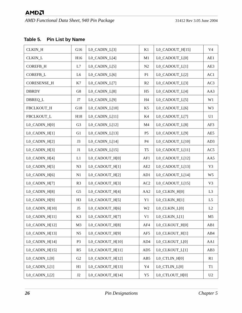
5 Pin Designations
Table 5, beginning on page 26, lists the pins alphabetically by pin name.
Chapter 5 Pin Designations 25
AMD Functional Data Sheet, 940 Pin Package 31412 Rev 3.05 June 2004
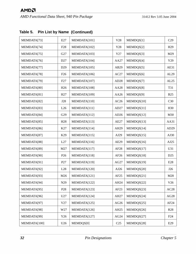
Table 5. Pin List by Name
CLKIN_H G16 L0_CADIN_L[3] K1 L0_CADOUT_H[15] V4
CLKIN_L H16 L0_CADIN_L[4] M1 L0_CADOUT_L[0] AE1
COREFB_H L7 L0_CADIN_L[5] N2 L0_CADOUT_L[1] AE3
COREFB_L L6 L0_CADIN_L[6] P1 L0_CADOUT_L[2] AC1
CORESENSE_H K7 L0_CADIN_L[7] R2 L0_CADOUT_L[3] AC3
DBRDY G8 L0_CADIN_L[8] H5 L0_CADOUT_L[4] AA3
DBREQ_L J7 L0_CADIN_L[9] H4 L0_CADOUT_L[5] W1
FBCLKOUT_H G18 L0_CADIN_L[10] K5 L0_CADOUT_L[6] W3
FBCLKOUT_L H18 L0_CADIN_L[11] K4 L0_CADOUT_L[7] U1
L0_CADIN_H[0] G3 L0_CADIN_L[12] M4 L0_CADOUT_L[8] AF3
L0_CADIN_H[1] G1 L0_CADIN_L[13] P5 L0_CADOUT_L[9] AE5
L0_CADIN_H[2] J3 L0_CADIN_L[14] P4 L0_CADOUT_L[10] AD3
L0_CADIN_H[3] J1 L0_CADIN_L[15] T5 L0_CADOUT_L[11] AC5
L0_CADIN_H[4] L1 L0_CADOUT_H[0] AF1 L0_CADOUT_L[12] AA5
L0_CADIN_H[5] N3 L0_CADOUT_H[1] AE2 L0_CADOUT_L[13] Y3
L0_CADIN_H[6] N1 L0_CADOUT_H[2] AD1 L0_CADOUT_L[14] W5
L0_CADIN_H[7] R3 L0_CADOUT_H[3] AC2 L0_CADOUT_L[15] V3
L0_CADIN_H[8] G5 L0_CADOUT_H[4] AA2 L0_CLKIN_H[0] L3
L0_CADIN_H[9] H3 L0_CADOUT_H[5] Y1 L0_CLKIN_H[1] L5
L0_CADIN_H[10] J5 L0_CADOUT_H[6] W2 L0_CLKIN_L[0] L2
L0_CADIN_H[11] K3 L0_CADOUT_H[7] V1 L0_CLKIN_L[1] M5
L0_CADIN_H[12] M3 L0_CADOUT_H[8] AF4 L0_CLKOUT_H[0] AB1
L0_CADIN_H[13] N5 L0_CADOUT_H[9] AF5 L0_CLKOUT_H[1] AB4
L0_CADIN_H[14] P3 L0_CADOUT_H[10] AD4 L0_CLKOUT_L[0] AA1
L0_CADIN_H[15] R5 L0_CADOUT_H[11] AD5 L0_CLKOUT_L[1] AB3
L0_CADIN_L[0] G2 L0_CADOUT_H[12] AB5 L0_CTLIN_H[0] R1
L0_CADIN_L[1] H1 L0_CADOUT_H[13] Y4 L0_CTLIN_L[0] T1
L0_CADIN_L[2] J2 L0_CADOUT_H[14] Y5 L0_CTLOUT_H[0] U2
26 Pin Designations Chapter 5

31412 Rev 3.05 June 2004 AMD Functional Data Sheet, 940 Pin Package
L0_CTLOUT_L[0] U3 L1_CADIN_H[13] /
NC_E161
E16 L1_CADIN_L[13] /
NC_E151
E15
L0_REF0 D1 L1_CADIN_H[14] /
NC_C151
C15 L1_CADIN_L[14] /
NC_D151
D15
L0_REF1 E1 L1_CADIN_H[15] /
NC_E141
E14 L1_CADIN_L[15] /
NC_E131
E13
L1_CADIN_H[0] /
NC_C221
C22 L1_CADIN_L[0] /
NC_B221
B22 L1_CADOUT_H[0] /
NC_A31
A3
L1_CADIN_H[1] /
NC_A221
A22 L1_CADIN_L[1] /
NC_A211
A21 L1_CADOUT_H[1] /
NC_B41
B4
L1_CADIN_H[2] /
NC_C201
C20 L1_CADIN_L[2] /
NC_B201
B20 L1_CADOUT_H[2] /
NC_A51
A5
L1_CADIN_H[3] /
NC_A201
A20 L1_CADIN_L[3] /
NC_A191
A19 L1_CADOUT_H[3] /
NC_B61
B6
L1_CADIN_H[4] /
NC_A181
A18 L1_CADIN_L[4] /
NC_A171
A17 L1_CADOUT_H[4] /
NC_B81
B8
L1_CADIN_H[5] /
NC_C161
C16 L1_CADIN_L[5] /
NC_B161
B16 L1_CADOUT_H[5] /
NC_A91
A9
L1_CADIN_H[6] /
NC_A161
A16 L1_CADIN_L[6] /
NC_A151
A15 L1_CADOUT_H[6] /
NC_B101
B10
L1_CADIN_H[7] /
NC_C141
C14 L1_CADIN_L[7] /
NC_B141
B14 L1_CADOUT_H[7] /
NC_A111
A11
L1_CADIN_H[8] /
NC_E221
E22 L1_CADIN_L[8] /
NC_E211
E21 L1_CADOUT_H[8] /
NC_D31
D3
L1_CADIN_H[9] /
NC_C211
C21 L1_CADIN_L[9] /
NC_D211
D21 L1_CADOUT_H[9] /
NC_E31
E3
L1_CADIN_H[10] /
NC_E201
E20 L1_CADIN_L[10] /
NC_E191
E19 L1_CADOUT_H[10] /
NC_D51
D5
L1_CADIN_H[11] /
NC_C191
C19 L1_CADIN_L[11] /
NC_D191
D19 L1_CADOUT_H[11] /
NC_E51
E5
L1_CADIN_H[12] /
NC_C171
C17 L1_CADIN_L[12] /
NC_D171
D17 L1_CADOUT_H[12] /
NC_E71
E7
Table 5. Pin List by Name (Continued)
Chapter 5 Pin Designations 27

AMD Functional Data Sheet, 940 Pin Package 31412 Rev 3.05 June 2004
L1_CADOUT_H[13] /
NC_D91
D9 L1_CADOUT_L[13] /
NC_C91
C9 L2_CADIN_H[1] /
NC_AL31
AL3
L1_CADOUT_H[14] /
NC_E91
E9 L1_CADOUT_L[14] /
NC_E101
E10 L2_CADIN_H[2] /
NC_AJ51
AJ5
L1_CADOUT_H[15] /
NC_D111
D11 L1_CADOUT_L[15] /
NC_C111
C11 L2_CADIN_H[3] /
NC_AL5 1AL5
L1_CADOUT_L[0] /
NC_A41
A4 L1_CLKIN_H[0] /
NC_C181
C18 L2_CADIN_H[4] /
NC_AL71
AL7
L1_CADOUT_L[1] /
NC_C41
C4 L1_CLKIN_H[1] /
NC_E181
E18 L2_CADIN_H[5] /
NC_AJ91
AJ9
L1_CADOUT_L[2] /
NC_A61
A6 L1_CLKIN_L[0] /
NC_B181
B18 L2_CADIN_H[6] /
NC_AL91
AL9
L1_CADOUT_L[3] /
NC_C61
C6 L1_CLKIN_L[1] /
NC_E171
E17 L2_CADIN_H[7] /
NC_AJ111
AJ11
L1_CADOUT_L[4] /
NC_C81
C8 L1_CLKOUT_H[0] /
NC_A71
A7 L2_CADIN_H[8] /
NC_AG31
AG3
L1_CADOUT_L[5] /
NC_A101
A10 L1_CLKOUT_H[1]/
NC_D71
D7 L2_CADIN_H[9] /
NC_AJ41
AJ4
L1_CADOUT_L[6] /
NC_C101
C10 L1_CLKOUT_L[0] /
NC_A81
A8 L2_CADIN_H[10] /
NC_AG51
AG5
L1_CADOUT_L[7] /
NC_A121
A12 L1_CLKOUT_L[1] /
NC_C71
C7 L2_CADIN_H[11] /
NC_AJ61
AJ6
L1_CADOUT_L[8] /
NC_C31
C3 L1_CTLIN_H[0] /
NC_A141
A14 L2_CADIN_H[12] /
NC_AJ81
AJ8
L1_CADOUT_L[9] /
NC_E41
E4 L1_CTLIN_L[0] /
NC_A131
A13 L2_CADIN_H[13] /
NC_AG91
AG9
L1_CADOUT_L[10] /
NC_C51
C5 L1_CTLOUT_H[0] /
NC_B121
B12 L2_CADIN_H[14] /
NC_AJ101
AJ10
L1_CADOUT_L[11] /
NC_E61
E6 L1_CTLOUT_L[0] /
NC_C121
C12 L2_CADIN_H[15] /
NC_AG111
AG11
L1_CADOUT_L[12] /
NC_E81
E8 L2_CADIN_H[0] /
NC_AJ31
AJ3 L2_CADIN_L[0] /
NC_AK31
AK3
Table 5. Pin List by Name (Continued)
28 Pin Designations Chapter 5

31412 Rev 3.05 June 2004 AMD Functional Data Sheet, 940 Pin Package
L2_CADIN_L[1] /
NC_AL41
AL4 L2_CADOUT_H[1] /
NC_AK211
AK21 L2_CADOUT_L[1] /
NC_AJ211
AJ21
L2_CADIN_L[2] /
NC_AK51
AK5 L2_CADOUT_H[2] /
NC_AL201
AL20 L2_CADOUT_L[2] /
NC_AL191
AL19
L2_CADIN_L[3] /
NC_AL61
AL6 L2_CADOUT_H[3] /
NC_AK191
AK19 L2_CADOUT_L[3] /
NC_AJ191
AJ19
L2_CADIN_L[4] /
NC_AL81
AL8 L2_CADOUT_H[4] /
NC_AK171
AK17 L2_CADOUT_L[4] /
NC_AJ171
AJ17
L2_CADIN_L[5] /
NC_AK91
AK9 L2_CADOUT_H[5] /
NC_AL161
AL16 L2_CADOUT_L[5] /
NC_AL151
AL15
L2_CADIN_L[6] /
NC_AL101
AL10 L2_CADOUT_H[6] /
NC_AK151
AK15 L2_CADOUT_L[6] /
NC_AJ151
AJ15
L2_CADIN_L[7] /
NC_AK111
AK11 L2_CADOUT_H[7] /
NC_AL141
AL14 L2_CADOUT_L[7] /
NC_AL131
AL13
L2_CADIN_L[8] /
NC_AG41
AG4 L2_CADOUT_H[8] /
NC_AH221
AH22 L2_CADOUT_L[8] /
NC_AJ221
AJ22
L2_CADIN_L[9] /
NC_AH41
AH4 L2_CADOUT_H[9] /
NC_AG221
AG22 L2_CADOUT_L[9] /
NC_AG211
AG21
L2_CADIN_L[10] /
NC_AG61
AG6 L2_CADOUT_H[10] /
NC_AH201
AH20 L2_CADOUT_L[10] /
NC_AJ201
AJ20
L2_CADIN_L[11] /
NC_AH61
AH6 L2_CADOUT_H[11] /
NC_AG201
AG20 L2_CADOUT_L[11] /
NC_AG191
AG19
L2_CADIN_L[12] /
NC_AH81
AH8 L2_CADOUT_H[12] /
NC_AG181
AG18 L2_CADOUT_L[12] /
NC_AG171
AG17
L2_CADIN_L[13] /
NC_AG101
AG10 L2_CADOUT_H[13] /
NC_AH161
AH16 L2_CADOUT_L[13] /
NC_AJ161
AJ16
L2_CADIN_L[14] /
NC_AH101
AH10 L2_CADOUT_H[14] /
NC_AG161
AG16 L2_CADOUT_L[14] /
NC_AG151
AG15
L2_CADIN_L[15] /
NC_AG121
AG12 L2_CADOUT_H[15] /
NC_AH141
AH14 L2_CADOUT_L[15] /
NC_AJ141
AJ14
L2_CADOUT_H[0] /
NC_AL221
AL22 L2_CADOUT_L[0] /
NC_AL211
AL21 L2_CLKIN_H[0] /
NC_AJ71
AJ7
Table 5. Pin List by Name (Continued)
Chapter 5 Pin Designations 29

AMD Functional Data Sheet, 940 Pin Package 31412 Rev 3.05 June 2004
L2_CLKIN_H[1] /
NC_AG71
AG7 MEMADD[8] L23 MEMCHECK[11] T27
L2_CLKIN_L[0] /
NC_AK71
AK7 MEMADD[9] K23 MEMCHECK[12] P25
L2_CLKIN_L[1] /
NC_AG81
AG8 MEMADD[10] V24 MEMCHECK[13] P24
L2_CLKOUT_H[0] /
NC_AL181
AL18 MEMADD[11] J25 MEMCHECK[14] T29
L2_CLKOUT_H[1] /
NC_AH181
AH18 MEMADD[12] J24 MEMCHECK[15] U28
L2_CLKOUT_L[0]/
NC_AL171
AL17 MEMADD[13] AE23 MEMCKE_LO H25
L2_CLKOUT_L[1] /
NC_AJ181
AJ18 MEMBANK[0] W23 MEMCKE_UP H24
L2_CTLIN_H[0] /
NC_AL111
AL11 MEMBANK[1] W25 MEMCLK_LO_H[0] U25
L2_CTLIN_L[0] /
NC_AL121
AL12 MEMCAS_L AA25 MEMCLK_LO_H[1] Y23
L2_CTLOUT_H[0] /
NC_AK131
AK13 MEMCHECK[0] R31 MEMCLK_LO_H[2] AD21
L2_CTLOUT_L[0] /
NC_AJ131
AJ13 MEMCHECK[1] R29 MEMCLK_LO_H[3] H23
LDTSTOP_L J6 MEMCHECK[2] U30 MEMCLK_LO_L[0] U24
MEMADD[0] V25 MEMCHECK[3] V31 MEMCLK_LO_L[1] AA23
MEMADD[1] T25 MEMCHECK[4] P30 MEMCLK_LO_L[2] AD20
MEMADD[2] P23 MEMCHECK[5] R30 MEMCLK_LO_L[3] J23
MEMADD[3] N23 MEMCHECK[6] U29 MEMCLK_UP_H[0] R23
MEMADD[4] N25 MEMCHECK[7] V30 MEMCLK_UP_H[1] L24
MEMADD[5] M24 MEMCHECK[8] R24 MEMCLK_UP_H[2] AE21
MEMADD[6] M25 MEMCHECK[9] R25 MEMCLK_UP_H[3] G20
MEMADD[7] K25 MEMCHECK[10] R26 MEMCLK_UP_L[0] T23
Table 5. Pin List by Name (Continued)
30 Pin Designations Chapter 5

31412 Rev 3.05 June 2004 AMD Functional Data Sheet, 940 Pin Package
MEMCLK_UP_L[1] L25 MEMDATA[17] F31 MEMDATA[45] AD31
MEMCLK_UP_L[2] AE20 MEMDATA[18] H31 MEMDATA[46] AF30
MEMCLK_UP_L[3] G21 MEMDATA[19] J31 MEMDATA[47] AG31
MEMCS_L[0] AA24 MEMDATA[20] F29 MEMDATA[48] AG30
MEMCS_L[1] AB25 MEMDATA[21] G31 MEMDATA[49] AH31
MEMCS_L[2] AC25 MEMDATA[22] J29 MEMDATA[50] AK28
MEMCS_L[3] AC24 MEMDATA[23] J30 MEMDATA[51] AL28
MEMCS_L[4] AD25 MEMDATA[24] K31 MEMDATA[52] AG29
MEMCS_L[5] AD24 MEMDATA[25] L31 MEMDATA[53] AJ31
MEMCS_L[6] AE25 MEMDATA[26] N31 MEMDATA[54] AK30
MEMCS_L[7] AD23 MEMDATA[27] P29 MEMDATA[55] AJ28
MEMDATA[0] B24 MEMDATA[28] L29 MEMDATA[56] AL27
MEMDATA[1] A25 MEMDATA[29] L30 MEMDATA[57] AL26
MEMDATA[2] A27 MEMDATA[30] M31 MEMDATA[58] AK24
MEMDATA[3] A28 MEMDATA[31] P31 MEMDATA[59] AL24
MEMDATA[4] A24 MEMDATA[32] V29 MEMDATA[60] AJ27
MEMDATA[5] C24 MEMDATA[33] Y30 MEMDATA[61] AK27
MEMDATA[6] A26 MEMDATA[34] AA30 MEMDATA[62] AK25
MEMDATA[7] B27 MEMDATA[35] AC31 MEMDATA[63] AJ24
MEMDATA[8] B28 MEMDATA[36] W31 MEMDATA[64] G23
MEMDATA[9] A29 MEMDATA[37] Y31 MEMDATA[65] E24
MEMDATA[10] E30 MEMDATA[38] AA29 MEMDATA[66] F25
MEMDATA[11] E31 MEMDATA[39] AB31 MEMDATA[67] E26
MEMDATA[12] C28 MEMDATA[40] AC29 MEMDATA[68] F23
MEMDATA[13] B30 MEMDATA[41] AD30 MEMDATA[69] D24
MEMDATA[14] C31 MEMDATA[42] AF31 MEMDATA[70] E25
MEMDATA[15] D31 MEMDATA[43] AF29 MEMDATA[71] C26
MEMDATA[16] F30 MEMDATA[44] AC30 MEMDATA[72] C27
Table 5. Pin List by Name (Continued)
Chapter 5 Pin Designations 31
AMD Functional Data Sheet, 940 Pin Package 31412 Rev 3.05 June 2004
MEMDATA[73] E27 MEMDATA[101] V28 MEMDQS[1] C29
MEMDATA[74] F28 MEMDATA[102] Y28 MEMDQS[2] H29
MEMDATA[75] G27 MEMDATA[103] Y27 MEMDQS[3] M29
MEMDATA[76] D27 MEMDATA[104] AA27 MEMDQS[4] Y29
MEMDATA[77] D29 MEMDATA[105] AB29 MEMDQS[5] AE31
MEMDATA[78] F26 MEMDATA[106] AC27 MEMDQS[6] AL29
MEMDATA[79] F27 MEMDATA[107] AD28 MEMDQS[7] AL25
MEMDATA[80] H26 MEMDATA[108] AA28 MEMDQS[8] T31
MEMDATA[81] H27 MEMDATA[109] AA26 MEMDQS[9] B25
MEMDATA[82] J28 MEMDATA[110] AC26 MEMDQS[10] C30
MEMDATA[83] L26 MEMDATA[111] AD27 MEMDQS[11] H30
MEMDATA[84] G29 MEMDATA[112] AD26 MEMDQS[12] M30
MEMDATA[85] H28 MEMDATA[113] AE27 MEMDQS[13] AA31
MEMDATA[86] K27 MEMDATA[114] AH29 MEMDQS[14] AD29
MEMDATA[87] K29 MEMDATA[115] AJ29 MEMDQS[15] AJ30
MEMDATA[88] L27 MEMDATA[116] AE29 MEMDQS[16] AJ25
MEMDATA[89] M27 MEMDATA[117] AF28 MEMDQS[17] U31
MEMDATA[90] P26 MEMDATA[118] AF26 MEMDQS[18] D25
MEMDATA[91] P27 MEMDATA[119] AG27 MEMDQS[19] E28
MEMDATA[92] L28 MEMDATA[120] AJ26 MEMDQS[20] J26
MEMDATA[93] M26 MEMDATA[121] AF25 MEMDQS[21] M28
MEMDATA[94] N29 MEMDATA[122] AH24 MEMDQS[22] V26
MEMDATA[95] P28 MEMDATA[123] AF23 MEMDQS[23] AC28
MEMDATA[96] U27 MEMDATA[124] AH27 MEMDQS[24] AG28
MEMDATA[97] V27 MEMDATA[125] AG26 MEMDQS[25] AF24
MEMDATA[98] W27 MEMDATA[126] AH25 MEMDQS[26] R28
MEMDATA[99] Y26 MEMDATA[127] AG24 MEMDQS[27] F24
MEMDATA[100] U26 MEMDQS[0] C25 MEMDQS[28] E29
Table 5. Pin List by Name (Continued)
32 Pin Designations Chapter 5

31412 Rev 3.05 June 2004 AMD Functional Data Sheet, 940 Pin Package
MEMDQS[29] J27 NC_AG14 AG14 NC_V5 V5
MEMDQS[30] N27 NC_AH12 AH12 NC_W6 W6
MEMDQS[31] W29 NC_AH2 AH2 PRESENCE_DET / VSS2 AK2
MEMDQS[32] AB27 NC_AJ12 AJ12 PWROK F12
MEMDQS[33] AF27 NC_AJ2 AJ2 RESET_L G12
MEMDQS[34] AG25 NC_C13 C13 TCK AE7
MEMDQS[35] R27 NC_D13 D13 TDI AF7
MEMRAS_L Y25 NC_E11 E11 TDO AE8
MEMRESET_L G25 NC_E12 E12 THERMDA AJ1
MEMVREF0 F22 NC_F7 F7 THERMDC AH1
MEMVREF1 AF22 NC_G14 G14 THERMTRIP_L AE15
MEMWE_L Y24 NC_G6 G6 TMS AE6
MEMZN AF17 NC_H12 H12 TRST_L AD7
MEMZP AE16 NC_H13 H13 VDD AA4
NC_AA6 AA6 NC_H14 H14 VDD AA9
NC_AC6 AC6 NC_H7 H7 VDD AA11
NC_AE10 AE10 NC_H9 H9 VDD AA13
NC_AE11 AE11 NC_K8 K8 VDD AA15
NC_AE12 AE12 NC_L8 L8 VDD AA17
NC_AE13 AE13 NC_M23 M23 VDD AB6
NC_AE14 AE14 NC_N6 N6 VDD AB8
NC_AE9 AE9 NC_R6 R6 VDD AB12
NC_AF11 AF11 NC_T3 T3 VDD AB18
NC_AF13 AF13 NC_T4 T4 VDD AC13
NC_AF15 AF15 NC_T7 T7 VDD AD2
NC_AF9 AF9 NC_U5 U5 VDD AD12
NC_AG1 AG1 NC_U6 U6 VDD AD14
NC_AG13 AG13 NC_V23 V23 VDD AD16
Table 5. Pin List by Name (Continued)
Chapter 5 Pin Designations 33

AMD Functional Data Sheet, 940 Pin Package 31412 Rev 3.05 June 2004
VDD AE4 VDD F19 VDD P10
VDD AF6 VDD G7 VDD P12
VDD AF10 VDD H2 VDD P14
VDD AF14 VDD J4 VDD P16
VDD AH5 VDD J13 VDD P18
VDD AH9 VDD K6 VDD P20
VDD AH13 VDD K12 VDD R9
VDD AH17 VDD K18 VDD R11
VDD AH21 VDD L9 VDD R13
VDD AK4 VDD L11 VDD R15
VDD AK8 VDD L13 VDD R17
VDD AK12 VDD L15 VDD R19
VDD AK16 VDD L17 VDD T2
VDD AK20 VDD M2 VDD T8
VDD B5 VDD M10 VDD T10
VDD B9 VDD M12 VDD T12
VDD B13 VDD M14 VDD T14
VDD B17 VDD M16 VDD T16
VDD B21 VDD M18 VDD T18
VDD D4 VDD M20 VDD T20
VDD D8 VDD N4 VDD U4
VDD D12 VDD N9 VDD U9
VDD D16 VDD N11 VDD U11
VDD D20 VDD N13 VDD U13
VDD F6 VDD N15 VDD U15
VDD F11 VDD N17 VDD U17
VDD F15 VDD N19 VDD U19
VDD F18 VDD P6 VDD V6
Table 5. Pin List by Name (Continued)
34 Pin Designations Chapter 5

31412 Rev 3.05 June 2004 AMD Functional Data Sheet, 940 Pin Package
VDD V10 VDDIO G26 VDDIO AA21
VDD V12 VDDIO G28 VDDIO AB20
VDD V14 VDDIO H22 VDDIO AB22
VDD V16 VDDIO J21 VDDIO AB26
VDD V18 VDDIO K20 VDDIO AB28
VDD V20 VDDIO K22 VDDIO AC21
VDD W9 VDDIO K26 VDDIO AD22
VDD W11 VDDIO K28 VDDIO AE26
VDD W13 VDDIO L19 VDDIO AE28
VDD W15 VDDIO L21 VDDIO AG23
VDD W17 VDDIO M22 VDDIO AH26
VDD W19 VDDIO N21 VDDIO AH28
VDD Y2 VDDIO N26 VDDIO AJ23
VDD Y10 VDDIO N28 VDDIO AL23
VDD Y12 VDDIO P22 VDDIO_SENSE AF20
VDD Y14 VDDIO R21 VDDIOFB_H AB23
VDD Y16 VDDIO T22 VDDIOFB_L AC23
VDD Y18 VDDIO T26 VID[0] G11
VDD Y20 VDDIO T28 VID[1] H11
VDDA1 / VDDA C1 VDDIO U21 VID[2] G10
VDDA2 / VDDA D2 VDDIO U23 VID[3] F9
VDDA3 / VDDA C2 VDDIO V22 VID[4] G9
VDDIO A23 VDDIO W21 VLDT_0 / VLDT3 M8
VDDIO C23 VDDIO W26 VLDT_0 / VLDT3 N7
VDDIO D26 VDDIO W28 VLDT_0 / VLDT3 P8
VDDIO D28 VDDIO Y22 VLDT_0 / VLDT3 R7
VDDIO E23 VDDIO AA19 VLDT_0 / VLDT3 U7
Table 5. Pin List by Name (Continued)
Chapter 5 Pin Designations 35

AMD Functional Data Sheet, 940 Pin Package 31412 Rev 3.05 June 2004
VLDT_0 / VLDT3 V8 VSS AA16 VSS AD15
VLDT_0 / VLDT3 W7 VSS AA18 VSS AD17
VLDT_0 / VLDT3 Y8 VSS AA20 VSS AE17
VLDT_0 / VLDT3 AA7 VSS AA22 VSS AE22
VLDT_1 / VLDT3 H8 VSS AB2 VSS AE24
VLDT_1 / VLDT3 H10 VSS AB7 VSS AE30
VLDT_1 / VLDT3 J9 VSS AB9 VSS AF2
VLDT_1 / VLDT3 J11 VSS AB11 VSS AF8
VLDT_1 / VLDT3 J15 VSS AB13 VSS AF12
VLDT_1 / VLDT3 J16 VSS AB15 VSS AF16
VLDT_1 / VLDT3 K10 VSS AB17 VSS AF21
VLDT_1 / VLDT3 K14 VSS AB19 VSS AG2
VLDT_1 / VLDT3 K16 VSS AB21 VSS AH3
VLDT_2 / VLDT3 AB10 VSS AB24 VSS AH7
VLDT_2 / VLDT3 AB14 VSS AB30 VSS AH11
VLDT_2 / VLDT3 AB16 VSS AC4 VSS AH15
VLDT_2 / VLDT3 AC9 VSS AC10 VSS AH19
VLDT_2 / VLDT3 AC11 VSS AC12 VSS AH23
VLDT_2 / VLDT3 AC15 VSS AC14 VSS AH30
VLDT_2 / VLDT3 AC16 VSS AC17 VSS AK6
VLDT_2 / VLDT3 AD8 VSS AC20 VSS AK10
VLDT_2 / VLDT3 AD10 VSS AC22 VSS AK14
VSS AA8 VSS AD6 VSS AK18
VSS AA10 VSS AD9 VSS AK22
VSS AA12 VSS AD11 VSS AK23
VSS AA14 VSS AD13 VSS AK26
Table 5. Pin List by Name (Continued)
36 Pin Designations Chapter 5

31412 Rev 3.05 June 2004 AMD Functional Data Sheet, 940 Pin Package
VSS AK29 VSS G15 VSS L12
VSS B3 VSS G17 VSS L14
VSS B7 VSS G22 VSS L16
VSS B11 VSS G24 VSS L18
VSS B15 VSS G30 VSS L20
VSS B19 VSS H6 VSS L22
VSS B23 VSS H15 VSS M6
VSS B26 VSS F10 VSS M7
VSS B29 VSS J8 VSS M9
VSS D6 VSS J10 VSS M11
VSS D10 VSS J12 VSS M13
VSS D14 VSS J14 VSS M15
VSS D18 VSS J17 VSS M17
VSS D22 VSS J18 VSS M19
VSS D23 VSS J20 VSS M21
VSS D30 VSS J22 VSS N8
VSS E2 VSS K2 VSS N10
VSS F1 VSS K9 VSS N12
VSS F2 VSS K11 VSS N14
VSS F5 VSS K13 VSS N16
VSS F8 VSS K15 VSS N18
VSS F10 VSS K17 VSS N20
VSS F13 VSS K19 VSS N22
VSS F14 VSS K21 VSS N24
VSS F16 VSS K24 VSS N30
VSS F17 VSS K30 VSS P2
VSS G4 VSS L4 VSS P7
VSS G13 VSS L10 VSS P9
Table 5. Pin List by Name (Continued)
Chapter 5 Pin Designations 37

AMD Functional Data Sheet, 940 Pin Package 31412 Rev 3.05 June 2004
Notes:1. Links 1 and 2 are available on Server/Workstation products only. No connect (NC_*) names apply to Desktop products.
VSS P11 VSS U8 VSS W20
VSS P13 VSS U10 VSS W22
VSS P15 VSS U12 VSS W24
VSS P17 VSS U14 VSS W30
VSS P19 VSS U16 VSS Y6
VSS P21 VSS U18 VSS Y7
VSS R4 VSS U20 VSS Y9
VSS R8 VSS U22 VSS Y11
VSS R10 VSS V2 VSS Y13
VSS R12 VSS V7 VSS Y15
VSS R14 VSS V9 VSS Y17
VSS R16 VSS V11 VSS Y19
VSS R18 VSS V13 VSS Y21
VSS R20 VSS V15 VTT AF18
VSS R22 VSS V17 VTT F20
VSS T6 VSS V19 VTT F21
VSS T9 VSS V21 VTT G19
VSS T11 VSS W4 VTT H19
VSS T13 VSS W8 VTT J19
VSS T15 VSS W10 VTT AC18
VSS T17 VSS W12 VTT AC19
VSS T19 VSS W14 VTT AE18
VSS T21 VSS W16 VTT AE19
VSS T24 VSS W18 VTT_SENSE AF19
VSS T30
Table 5. Pin List by Name
38 Pin Designations Chapter 5

31412 Rev 3.05 June 2004 AMD Functional Data Sheet, 940 Pin Package
2. PRESENCE_DET is used for Server/Workstation products only. This pin should be connected to VSS for Desktop products. See the AMD Athlon™ 64 FX and AMD Opteron™ Processor Motherboard Design Guide, order# 25180, for connection details.
3. VLDT is referenced as a unified plane for Desktop products.
Chapter 5 Pin Designations 39

AMD Functional Data Sheet, 940 Pin Package 31412 Rev 3.05 June 2004
40 Pin Designations Chapter 5

31412 Rev 3.05 June 2004 AMD Functional Data Sheet, 940 Pin Package
6 Pin Descriptions
Table 6 describes the terms used in the pin description tables found in this chapter. The pins are organized within the following functional groups:
• HyperTransport™ technology interface
• DDR SDRAM memory interface
• Miscellaneous pins, including clock, JTAG, and debug pins
All pins are described in the tables beginning on page 42.
Table 6. Pin Description Table Definitions
Notes:1. Refer to Table 36, “Combined AC and DC Operating Conditions for Power Supplies,” on page 75 for VDDIO voltage
specifications.
Pin Types Applicable Section in Electrical Chapter
I-HT Input, HyperTransport™ technology, Differential “HyperTransport™ Technology Interface” on page 50
O-HT Output, HyperTransport™ technology, Differential
“HyperTransport™ Technology Interface” on page 50
B-IOS Bidirectional, VDDIO1 Single-Ended “DDR SDRAM and Miscellaneous Pins” on page 53
I-IOS Input, VDDIO1, Single-Ended “DDR SDRAM and Miscellaneous Pins” on page 53
I-IOD Input, VDDIO1, Differential “Clock Pins” on page 65
O-IOD Output, VDDIO1, Differential “Clock Pins” on page 65
O-IOS Output, VDDIO1, Single-Ended “DDR SDRAM and Miscellaneous Pins” on page 53
O-IO-OD Output, VDDIO1, Open Drain “DDR SDRAM and Miscellaneous Pins” on page 53
A Analog “Power Supplies” on page 75
S Supply Voltage “Power Supplies” on page 75
VREF Voltage Reference “DDR SDRAM and Miscellaneous Pins” on page 53
Chapter 6 Pin Descriptions 41

AMD Functional Data Sheet, 940 Pin Package 31412 Rev 3.05 June 2004
6.1 HyperTransport™ Technology Pins
Notes:1. These pins are used in an alternating fashion to compensate RTT by internal comparison to 3/4 VLDT and 1/4 VLDT
and compensate RON by comparison to each other around 1/2 VLDT. For proper resistor value, see the AMD
Athlon™ 64 FX and AMD Opteron™ Processor Motherboard Design Guide, order# 25180.2. Link 1 and Link 2 are available only on Server products.
Table 7. HyperTransport™ Technology Pin Descriptions
Signal Name Type Description
L0_CLKIN_H/L[1:0] I-HT Link 0 Clock Input
L0_CTLIN_H/L[0] I-HT Link 0 Control Input
L0_CADIN_H/L[15:0] I-HT Link 0 Command/Address/Data Input
L0_CLKOUT_H/L[1:0] O-HT Link 0 Clock Outputs
L0_CTLOUT_H/L[0] O-HT Link 0 Control Output
L0_CADOUT_H/L[15:0] O-HT Link 0 Command/Address/Data Outputs
L1_CLKIN_H/L[1:0]2 I-HT Link 1 Clock Input
L1_CTLIN_H/L[0]2 I-HT Link 1 Control Input
L1_CADIN_H/L[15:0]2 I-HT Link 1 Command/Address/Data Input
L1_CLKOUT_H/L[1:0]2 O-HT Link 1 Clock Outputs
L1_CTLOUT_H/L[0]2 O-HT Link 1 Control Output
L1_CADOUT_H/L[15:0]2 O-HT Link 1 Command/Address/Data Outputs
L2_CLKIN_H/L[1:0]2 I-HT Link 2 Clock Input
L2_CTLIN_H/L[0]2 I-HT Link 2 Control Input
L2_CADIN[15:0]2 I-HT Link 2 Command/Address/Data Input
L2_CLKOUT_H/L[1:0]2 O-HT Link 2 Clock Outputs
L2_CTLOUT_H/L[0]2 O-HT Link 2 Control Output
L2_CADOUT_H/L[15:0]2 O-HT Link 2 Command/Address/Data Outputs
L0_REF1 A Compensation Resistor to VLDT1
L0_REF0 A Compensation Resistor to VSS1
42 Pin Descriptions Chapter 6

31412 Rev 3.05 June 2004 AMD Functional Data Sheet, 940 Pin Package
6.2 DDR SDRAM Memory Interface Pins
Table 8. DDR SDRAM Memory Interface Pin Descriptions
Signal Name Type Description
MEMCLK_UP_H/L[3] O-IOD DRAM Clock connected to DIMM3 for the upper half of the data bus
MEMCLK_UP_H/L[2] O-IOD DRAM Clock connected to DIMM2 for the upper half of the data bus
MEMCLK_UP_H/L[1] O-IOD DRAM Clock connected to DIMM1 for the upper half of the data bus
MEMCLK_UP_H/L[0] O-IOD DRAM Clock connected to DIMM0 for the upper half of the data bus
MEMCLK_LO_H/L[3] O-IOD DRAM Clock connected to DIMM3 for the lower half of the data bus
MEMCLK_LO_H/L[2] O-IOD DRAM Clock connected to DIMM2 for the lower half of the data bus
MEMCLK_LO_H/L[1] O-IOD DRAM Clock connected to DIMM1 for the lower half of the data bus
MEMCLK_LO_H/L[0] O-IOD DRAM Clock connected to DIMM0 for the lower half of the data bus
MEMCKE_UP O-IOS DRAM Clock Enable
MEMCKE_LO O-IOS DRAM Clock Enable
MEMDQS[35:0] B-IOS DRAM Data Strobe synchronous with MEMCHECK[15:12] for x4 DIMMs.
MEMDQS[34:27] B-IOS DRAM Data Strobe synchronous with the high-order nibbles of MEMDATA[127:64] for x4 DIMMs
MEMDQS[26] B-IOS DRAM data strobe synchronous with MEMCHECK[11:8] for x4 DIMMs and MEMCHECK[15:8] for x8/x16 DIMMs.
MEMDQS[25:18] B-IOS DRAM Data Strobe synchronous with the low-order nibbles of MEMDATA[127:64] for x4 DIMMs and all nibbles for x8/x16 DIMMs
MEMDQS[17] B-IOS DRAM Data Strobe synchronous with MEMCHECK[7:4] for x4 DIMMs
MEMDQS[16:9] B-IOS DRAM Data Strobe synchronous with high-order nibbles of MEMDATA[63:0] for x4 DIMMs
MEMDQS[8] B-IOS DRAM Data Strobe synchronous with MEMCHECK[3:0] for x4 DIMMs and MEMCHECK[7:0] for x8/x16 DIMMs
MEMDQS[7:0] B-IOS DRAM Data Strobe synchronous with low-order nibbles of MEMDATA[127:64] for x4 DIMMs and all nibbles for x8/x16 DIMMs
MEMDATA[127:0] B-IOS DRAM Interface Data Bus
MEMCHECK[15:0] B-IOS DRAM Interface ECC Check Bits
MEMCS_L[7:0] O-IOS DRAM Chip Selects1
MEMRAS_L O-IOS DRAM Row Address Select
MEMCAS_L O-IOS DRAM Column Address Select
Chapter 6 Pin Descriptions 43

AMD Functional Data Sheet, 940 Pin Package 31412 Rev 3.05 June 2004
Notes:1. For connection details and proper resistor values, see the AMD Athlon™ 64 FX and AMD Opteron™ Processor
Motherboard Design Guide, order# 25180.
MEMWE_L O-IOS DRAM Write Enable
MEMADD[13:0] O-IOS DRAM Column/Row Address
MEMBANK[1:0] O-IOS DRAM Bank Address
MEMRESET_L O-IOS DRAM Reset pin for Suspend-to-RAM power management mode. This pin is required for registered DIMMs only.
MEMVREF VREF DRAM Interface Voltage Reference1
MEMZP A Compensation Resistor tied to VSS1
MEMZN A Compensation Resistor tied to VDDIO1
Table 8. DDR SDRAM Memory Interface Pin Descriptions (Continued)
Signal Name Type Description
44 Pin Descriptions Chapter 6

31412 Rev 3.05 June 2004 AMD Functional Data Sheet, 940 Pin Package
6.3 Miscellaneous Pins
Table 9. Clock Pin Descriptions
Signal Name Type Description
CLKIN_H/L I-IOD 200-MHz PLL Reference Clock
FBCLKOUT_H/L O-IOD Core Clock PLL 200-MHz Feedback Clock
Table 10. Miscellaneous Pin Descriptions
Signal Name Type Description
RESET_L I-IOS System Reset
PWROK I-IOS Indicates that voltages and clocks have reached specified operation
LDTSTOP_L I-IOS HyperTransport™ Technology Stop Control Input. Used for power management and for changing HyperTransport™ link width and frequency.
VID[4:0] O-IOS Voltage ID to the regulator
THERMDA A Anode (+) of the thermal diode
THERMDC A Cathode (–) of the thermal diode
THERMTRIP_L O-IO-OD Thermal Sensor Trip output, asserted at nominal temperature of 125oC.
COREFB_H/L A Differential feedback for VDD Power Supply
VDDIOFB_H/L A Differential feedback for VDDIO Power Supply
CORE_SENSE A VDD voltage monitor pin
VDDA S Filtered PLL Supply Voltage
VTT_SENSE A VTT voltage monitor pin
VDDIO_SENSE A VDDIO voltage monitor pin
VDD S Core power supply
VDDIO S DDR SDRAM I/O ring power supply
VLDT_01
VLDT_11
VLDT_21
S HyperTransport™ I/O ring power supply
VTT S VTT regulator voltage
Chapter 6 Pin Descriptions 45

AMD Functional Data Sheet, 940 Pin Package 31412 Rev 3.05 June 2004
Notes:1. VLDT is referenced as a unified plane for Desktop products.2. PRESENCE_DET is used for Server/Workstation products only. This pin should be connected to VSS for Desktop
products. See the AMD Athlon™ 64 FX and AMD Opteron™ Processor Motherboard Design Guide, order# 25180, for connection details.
PRESENCE_DET2 S This pin can be connected to VSS or used for detection of the processor in multiprocessor configurations. When used as a presence detection bit it should be pulled up and sensed via the circuitry that is used to detect installed processors on the motherboard. This pin is connected to VSS internally.
VSS S Ground
Table 11. VID[4:0] Encoding
VID[4:0] VDD VID[4:0] VDD VID[4:0] VDD VID[4:0] VDD
0x00000 1.550 V 0x01000 1.350 V 0x10000 1.150 V 0x11000 0.950 V
0x00001 1.525 V 0x01001 1.325 V 0x10001 1.125 V 0x11001 0.925 V
0x00010 1.500 V 0x01010 1.300 V 0x10010 1.100 V 0x11010 0.900 V
0x00011 1.475 V 0x01011 1.275 V 0x10011 1.075 V 0x11011 0.875 V
0x00100 1.450 V 0x01100 1.250 V 0x10100 1.050 V 0x11100 0.850 V
0x00101 1.425 V 0x01101 1.225 V 0x10101 1.025 V 0x11101 0.825 V
0x00110 1.400 V 0x01110 1.200 V 0x10110 1.000 V 0x11110 0.800 V
0x00111 1.375 V 0x01111 1.175 V 0x10111 0.975 V 0x11111 Off
Table 12. JTAG Pin Descriptions
Signal Name Type Description
TCK I-IOS JTAG Clock
TMS I-IOS JTAG Mode Select
TRST_L I-IOS JTAG Reset
TDI I-IOS JTAG Data Input
TDO O-IOS JTAG Data Output
Table 10. Miscellaneous Pin Descriptions (Continued)
Signal Name Type Description
46 Pin Descriptions Chapter 6
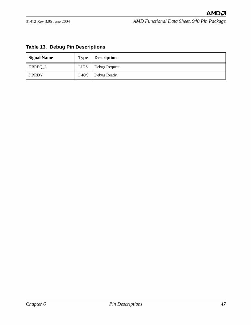
31412 Rev 3.05 June 2004 AMD Functional Data Sheet, 940 Pin Package
Table 13. Debug Pin Descriptions
Signal Name Type Description
DBREQ_L I-IOS Debug Request
DBRDY O-IOS Debug Ready
Chapter 6 Pin Descriptions 47

AMD Functional Data Sheet, 940 Pin Package 31412 Rev 3.05 June 2004
6.4 Pin States at ResetThe default pin states are listed below. These are listed for all output and bidirectional pins in the power-on reset state (reset) as well as the ACPI S1 and S3 power management states.
For differential inputs, “0” and “1” refer to the high-end differential output. Low-end differential outputs are inverted.Definitions of pin states: X: Either logic 1 or 0, Z: Tristated, T: Toggling between 0 and 1
Table 14. Reset Pin State
Pin NameResetState
S1State
S3State
Comments
L*_CLKOUT* T Z Z Tristated in S1 only if programmed to do so.
L*_CTLOUT* 0 Z Z Tristated in S1 only if programmed to do so.
L*_CADOUT* 1 Z Z Tristated in S1 only if programmed to do so.
MEMCLK* Z Z Z
MEMDQS* Z Z Z
MEMCKE* 0 0 0 In S3, MEMCKE* is forced to a logic Low.
MEMDATA* Z Z Z
MEMCHECK* Z Z Z
MEMCS_L* 1 Z Z
MEMRAS_L 1 Z Z
MEMCAS_L 1 Z Z
MEMWE_L 1 Z Z
MEMADD* 0 Z Z
MEMBANK* 0 Z Z
MEMRESET_L 0 0 0 In S3, MEMRESET_L is forced to logic 0.
MEMZN 1 1 1
MEMZP 0 0 0
FBCLKOUT* T T Z
TDO X X Z
DBRDY 0 0 Z
VID[4:0] X X X
THERMTRIP_L Z X Z
48 Pin Descriptions Chapter 6

31412 Rev 3.05 June 2004 AMD Functional Data Sheet, 940 Pin Package
7 Electrical Data
7.1 Absolute Maximum RatingsStresses greater than those listed in Table 15 may cause permanent damage to the device and motherboard. Systems using this device must be designed to ensure that these parameters are not violated. Violation of these ratings will void the product warranty. Exposure to absolute maximum rating conditions for extended periods may affect device reliability.
Refer to AMD Opteron™ Processor Power and Thermal Data Sheet, order# 30417, for maximum case temperature specifications.
Table 15. Absolute Maximum Ratings
Characteristic Range
Storage Temperature –55oC to 85oC
VLDT supply voltage relative to VSS –0.3 V to 1.5 V
VDD supply voltage relative to VSS –0.3 V to 1.65 V
VTT supply voltage relative to VSS –0.3 V to 1.65 V
VDDIO supply voltage relative to VSS –1 V to 2.9 V
VDDA supply voltage relative to VSS –0.3 V to 3.0 V
MEMVREF input voltage relative to VSS –1 V to 2.9 V
Input voltage relative to VSS for HyperTransport™ technology interface –0.3 V to 1.5 V
Differential input voltage for HyperTransport™ technology interface –1.5 V to 1.5 V
Input voltage relative to VSS for DDR SDRAM memory interface and Miscellaneous pins
–1 V to 2.9V
Chapter 7 Electrical Data 49

AMD Functional Data Sheet, 940 Pin Package 31412 Rev 3.05 June 2004
7.2 HyperTransport™ Technology Interface
7.2.1 Operating Conditions
Notes:1. Measured by comparing each signal voltage with respect to ground.2. Measured at <100 MHz, considered slow enough to attain both 0 and 1 logic state voltage levels without AC
transients on signals and supplies.
Table 16. DC Operating Conditions for HyperTransport™ Technology Interface
Symbol Parameter Unit Min Typ Max Notes
VOD Output Differential Voltage mV 495 600 715 1, 2
VOCM Output Common Mode Voltage mV 495 600 715 1, 2
VID Input Differential Voltage mV 200 600 1000 1, 2
VICM Input Common Mode Voltage mV 440 600 780 1, 2
DeltaVOD Change in VOD from 0 to 1 State mV –15 0 15 1
DeltaVOCM Change in VOCM from 0 to 1 State mV –15 0 15 1
DeltaVID Change in VID from 0 to 1 State mV –15 0 15 1
DeltaVICM Change in VICM from 0 to 1 State mV –15 0 15 1
Il Input Leakage Current mA –1 1
IOZ Output Tristate Leakage Current mA –1 1
RON Output Driver Impedance ohm 45 50 55
DeltaRON Change in RON Driving 0=>1 or
1=>0
% –2.5 0 2.5
RTT Input Differential Impedance ohm 90 100 110
50 Electrical Data Chapter 7

31412 Rev 3.05 June 2004 AMD Functional Data Sheet, 940 Pin Package
Notes:1. Measured by comparing each signal voltage with respect to ground.2. Measured in a differential fashion relative to the complement signal.3. Measured from crossing points of differential pairs.4. Input setup and hold times are measured from the crossing point of CAD versus the crossing point of CLK, effectively
including the edge time to achieve VID min AC.
Table 17. AC Operating Conditions for HyperTransport™ Technology Interface
Symbol Parameter Unit Min Typ Max Notes
VOD Output Differential Voltage mV 400 820 1
VOCM Output Common Mode Voltage mV 440 780 1
VID Input Differential Voltage mV 300 900 1
VICM Input Common Mode Voltage mV 385 845 1
DeltaVOD Change in VOD from 0 to 1 State mV –75 75 1
DeltaVOCM Change in VOCM from 0 to 1 State mV –50 50 1
DeltaVID Change in VID from 0 to 1 State mV –125 125 1
DeltaVICM Change in VICM from 0 to 1 State mV –100 100 1
TRISE Input Rising Edge Rate V/ns 1 4 1, 2
TFALL Input Falling Edge Rate V/ns 1 4 1, 2
CIN Input Pad Capacitance pF 2
COUT Output Pad Capacitance pF 3
CDELTA CIN Pad Capacitance Range Across Group pF 0.5
TCADV Output CAD Valid pS 166 459 3
TPHERR Accumulated Phase Error, CLKIN_H/L to L*_CLKOUT_H/L[1:0]
pS 0 5000
TSU Device Setup Time pS 110 3, 4
THLD Device Hold Time pS 110 3, 4
RTT Input Differential Impedance ohm 90 100 110
RON Output Impedance ohm 45 50 55
DeltaRON Change in RON Driving 0=>1 or 1=>0 % –2.5 2.5
Chapter 7 Electrical Data 51

AMD Functional Data Sheet, 940 Pin Package 31412 Rev 3.05 June 2004
7.2.2 Reference Information
Table 18. Internal Termination for HyperTransport™ Technology Interface
Pin Internal Termination Value Tolerance
L*_CADIN* Differential RTT 100 ohm (PVT-compensated) ±10%
L*_CTLIN* Differential RTT 100 ohm (PVT-compensated) ±10%
L*_CLKIN* Differential RTT 100 ohm (PVT-compensated) ±10%
52 Electrical Data Chapter 7
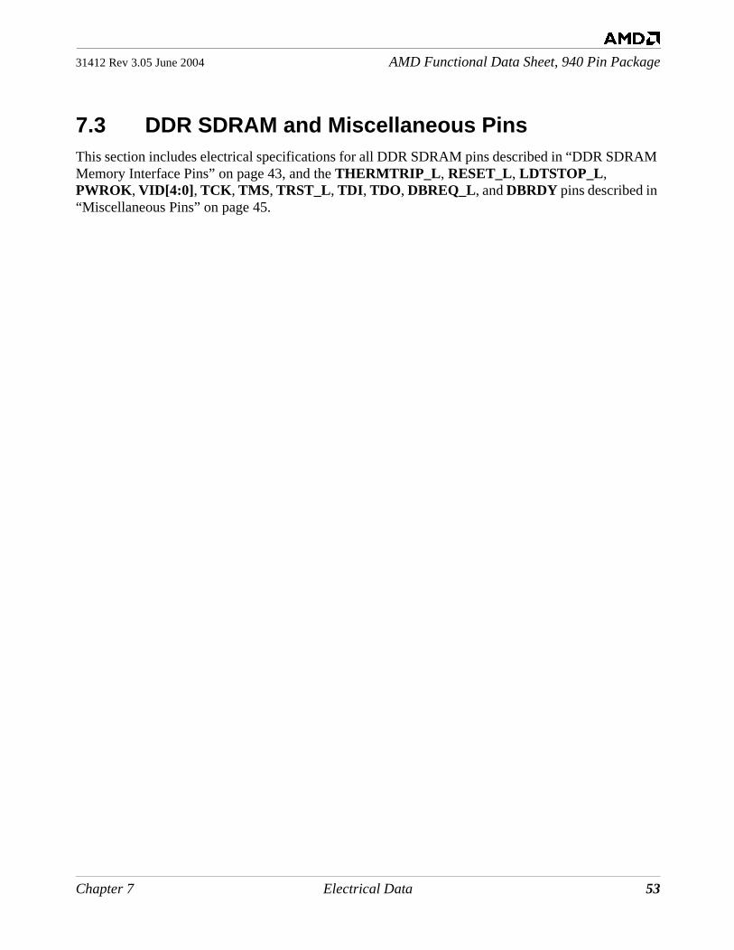
31412 Rev 3.05 June 2004 AMD Functional Data Sheet, 940 Pin Package
7.3 DDR SDRAM and Miscellaneous PinsThis section includes electrical specifications for all DDR SDRAM pins described in “DDR SDRAM Memory Interface Pins” on page 43, and the THERMTRIP_L, RESET_L, LDTSTOP_L, PWROK, VID[4:0], TCK, TMS, TRST_L, TDI, TDO, DBREQ_L, and DBRDY pins described in “Miscellaneous Pins” on page 45.
Chapter 7 Electrical Data 53

AMD Functional Data Sheet, 940 Pin Package 31412 Rev 3.05 June 2004
7.3.1 Operating Conditions
Notes:The notes for Table 19 through Table 22 appear on page 56.
Table 19. DC Operating Conditions
Symbol Parameters Unit Min Typ Max Notes
Vref Reference voltage (for I/O), MEMVREF pin
V 0.49*VDDIO_dc
Min
0.5*VDDIO_dc 0.51*VDDIO_dc
Max
1, 12
Il Input leakage currentAny input: 0 < VIN < VDDIO V
(All other pins not under test = 0V)
mA -1 1
Ioz Output leakage currentAny output: 0 < VOUT <
VDDIO V
mA -1 1
VIH Input high voltage (logic 1) V Vref + 0.15 - - 2
VIL Input low voltage (logic 0) V - - Vref - 0.15 2
VOH
Output high voltage (logic 1) (for VID[4:0])
V 2.0
Output high voltage (logic 1) (for all other pins)
V 1.8
VOL Output low voltage (logic 0) V 0.65
IOH Output levels -Output high cur-rent (VOUT= VDDIO/2)
mA -25 -28 -33 3
IOL Output levels - Output low cur-rent (VOUT=VDDIO/2)
mA 25 28 32 3
VOD Differential output voltage (for CK & CK)
V 1.2 1.3 1.4 4
VOD Change in VOD magnitude mV -100 - 100 5
VOCM Output common mode voltage (for CK & CK)
V 1.1 1.25 1.4 6
VOCM Change in VOCM magnitude mV -100 - 100 7
∆
∆
54 Electrical Data Chapter 7

31412 Rev 3.05 June 2004 AMD Functional Data Sheet, 940 Pin Package
Table 20. AC Operating Conditions
Symbol Parameters Unit Min Typ Max Notes
Vref Reference voltage (for I/O), MEMVREF pin
V Vref(DC) - 2%
Vref(DC) + 2%
1
VIH Input high voltage (logic 1) V Vref + 0.35 - 2
VIL Input low voltage (logic 0) V - Vref - 0.35 2
VOD Differential output voltage (for CK & CK)
V 1.0 1.3 1.6 4
VOD Change in VOD magnitude mV -150 - 150 5
VOCM Output common mode voltage (for CK & CK)
V 0.9 1.25 1.6 6
VOCM Change in VOCM magnitude mV -200 - 200 7
Table 21. Input Capacitance
Symbol Parameters Unit Min Typ Max Notes
Cin Input capacitance (DQ & DQS) pF 3.0 3.5 4.0
C Delta Input capacitance pF - - 0.4 8
Table 22. Slew Rate of DDR SDRAM Signals
Symbol Parameters Unit Min Typ Max Notes
SOUT Output slew rate (pullup and pull-down)
V/ns 2 3 4 9
SOUT_Ratio
Output slew rate ratio between pullup and pulldown
0.75 1 1.25 10
Sin Input slew rate V/ns 0.5 4 11
∆
∆
∆
Chapter 7 Electrical Data 55
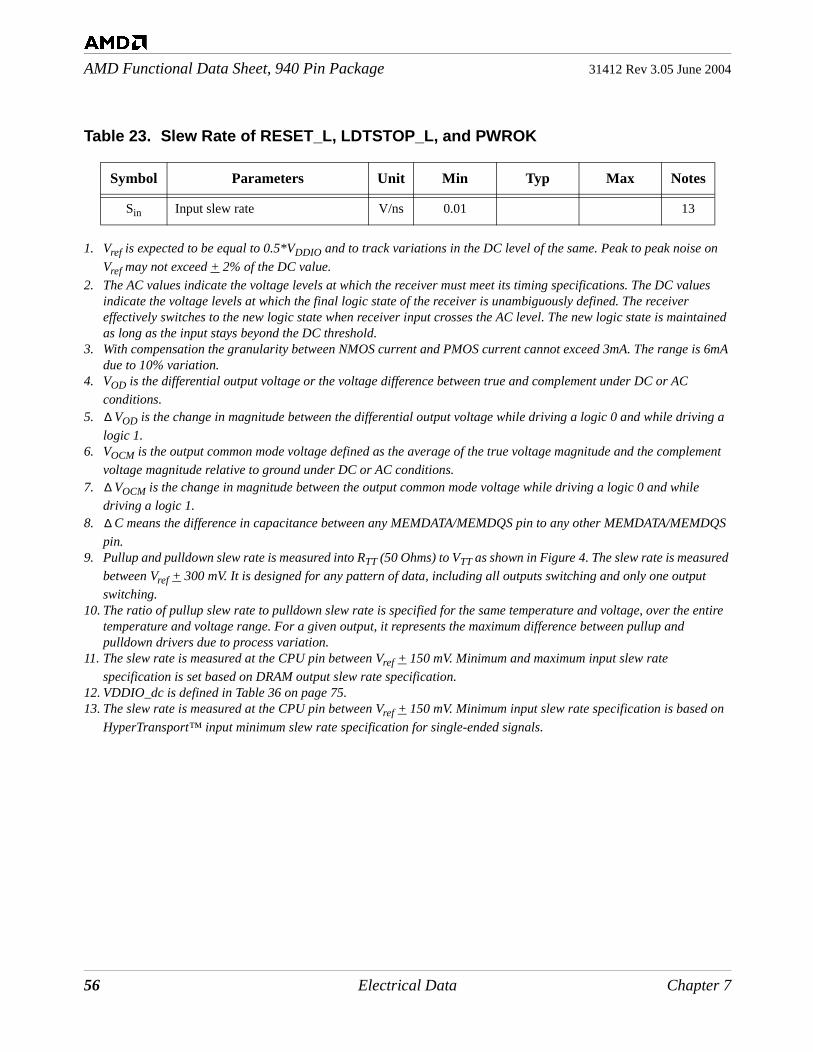
AMD Functional Data Sheet, 940 Pin Package 31412 Rev 3.05 June 2004
Table 23. Slew Rate of RESET_L, LDTSTOP_L, and PWROK
1. Vref is expected to be equal to 0.5*VDDIO and to track variations in the DC level of the same. Peak to peak noise on
Vref may not exceed + 2% of the DC value.
2. The AC values indicate the voltage levels at which the receiver must meet its timing specifications. The DC values indicate the voltage levels at which the final logic state of the receiver is unambiguously defined. The receiver effectively switches to the new logic state when receiver input crosses the AC level. The new logic state is maintained as long as the input stays beyond the DC threshold.
3. With compensation the granularity between NMOS current and PMOS current cannot exceed 3mA. The range is 6mA due to 10% variation.
4. VOD is the differential output voltage or the voltage difference between true and complement under DC or AC
conditions.5. VOD is the change in magnitude between the differential output voltage while driving a logic 0 and while driving a
logic 1.6. VOCM is the output common mode voltage defined as the average of the true voltage magnitude and the complement
voltage magnitude relative to ground under DC or AC conditions.7. VOCM is the change in magnitude between the output common mode voltage while driving a logic 0 and while
driving a logic 1.8. C means the difference in capacitance between any MEMDATA/MEMDQS pin to any other MEMDATA/MEMDQS
pin.9. Pullup and pulldown slew rate is measured into RTT (50 Ohms) to VTT as shown in Figure 4. The slew rate is measured
between Vref + 300 mV. It is designed for any pattern of data, including all outputs switching and only one output
switching.10. The ratio of pullup slew rate to pulldown slew rate is specified for the same temperature and voltage, over the entire
temperature and voltage range. For a given output, it represents the maximum difference between pullup and pulldown drivers due to process variation.
11. The slew rate is measured at the CPU pin between Vref + 150 mV. Minimum and maximum input slew rate
specification is set based on DRAM output slew rate specification.12. VDDIO_dc is defined in Table 36 on page 75.13. The slew rate is measured at the CPU pin between Vref + 150 mV. Minimum input slew rate specification is based on
HyperTransport™ input minimum slew rate specification for single-ended signals.
Symbol Parameters Unit Min Typ Max Notes
Sin Input slew rate V/ns 0.01 13
∆
∆
∆
56 Electrical Data Chapter 7

31412 Rev 3.05 June 2004 AMD Functional Data Sheet, 940 Pin Package
Figure 4. Slew Rate Measurement Example
Table 24. Package Routing Skew
Routing Measurement Skew (ps)
Any MEMCLK clock pair to any other MEMCLK clock pair + 100
Any MEMCLK pair to any MEMDQS pair + 100
Any MEMDQS pair to any MEMDATA associated within pair + 75
Any MEMCLK pair to any MEMADD/CMD + 100
Pad skew + 250
RTT
VTT
0 pF
Driver
Chapter 7 Electrical Data 57
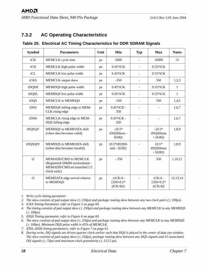
AMD Functional Data Sheet, 940 Pin Package 31412 Rev 3.05 June 2004
7.3.2 AC Operating Characteristics
1. Write cycle timing parameter2. The skew consists of pad output skew (+ 250ps) and package routing skew between any two clock pairs (+ 100ps).3. tCKS Timing Parameter, refer to Figure 5 on page 60.4. The timing consists of pad output skew (+ 250ps) and package routing skew between any MEMCLK to any MEMDQS
(+ 100ps).5. tDQS Timing parameter, refer to Figure 6 on page 60.6. The skew consists of pad output skew (+ 250ps) and package routing skew between any MEMCLK to any MEMDQS
(+ 100ps). Minimum DQS pulse width is 45% of MEMCLK.7. tDSS, tDSH timing parameters, refer to Figure 7 on page 61.8. During write, DQ signals are driven quarter clock earlier such that DQS is placed in the center of data eye window.
The skew consists of pad output skew (+ 250ps), package routing skew between any DQS signals and it’s associated DQ signals (+ 75ps) and maximum clock granularity (+ 312.5 ps).
Table 25. Electrical AC Timing Characteristics for DDR SDRAM Signals
Symbol Parameters Unit Min Typ Max Notes
tCK MEMCLK cycle time ps 5000 - 10000 15
tCH MEMCLK high pulse width ps 0.45*tCK - 0.55*tCK
tCL MEMCLK low pulse width ps 0.45*tCK - 0.55*tCK
tCKS MEMCLK output skew ps -350 - 350 1,2,3
tDQSH MEMDQS high pulse width ps 0.45*tCK - 0.55*tCK 1
tDQSL MEMDQS low pulse width ps 0.45*tCK - 0.55*tCK 1
tDQS MEMCLK to MEMDQS ps -350 - 350 1,4,5
tDSS MEMDQS falling edge to MEM-CLK rising edge
ps 0.45*tCK - 350
- - 1,6,7
tDSH MEMCLK rising edge to MEM-DQS falling edge
ps 0.45*tCK - 350
- - 1,6,7
tDQSQV MEMDQS to MEMDATA shift(when data becomes valid)
ps -{0.5* tDQSHmax -
[638]}
- -{0.5* tDQSHmin
+ [638]}
1,8,9
tDQSQIV MEMDQS to MEMDATA shift(when data becomes invalid)
ps {0.5*tDQSH-min - [638]}
- {0.5* tDQSHmax
+ [638]}
1,8,9
t2 MEMADD/CMD to MEMCLK (Registered DIMM environment - MEMADD/CMD are launched 1/2 clock early)
ps - 350 - 350 1,10,11
t3 MEMDATA edge arrival relative to MEMDQS
ps -{tCK/4 - [350+0.2*(tCK/4)]}
- tCK/4 - [350+0.2* (tCK/4)]
12,13,14
58 Electrical Data Chapter 7

31412 Rev 3.05 June 2004 AMD Functional Data Sheet, 940 Pin Package
9. tDQSQV and tDQSQIV timing parameters apply only within DQS and its associated DQ signals. Refer to Figure 8 on page 62.
10. The skew consists of pad output skew (+ 250 ps) and package routing skew (+ 100 ps) between any MEMCLK pair to any MEMADD/CMD signal. Maximum clock granularity skew is 312.5 ps.
11. t2 Timing parameter, applies to registered DIMM Environment Only - MEMADD/CMD signals are launched 1/2 clock cycle early. The granularity term does not apply here. Refer to Figure 9 on page 63.
12. Read cycle timing parameter.13. The PDL placement uncertainty is 20%. Package skew between DQS and its associated DQs is 75ps. The sum of
setup/hold time & receiver uncertainty is 275ps.14. t3 timing parameter, refer to Figure 10 on page 64.15. The slow operation of 10ns cycle time is specifically included for functional test purpose only. All electrical
characterization will be performed at full speed however all functional tests will be performed at 10ns cycle time.
Chapter 7 Electrical Data 59

AMD Functional Data Sheet, 940 Pin Package 31412 Rev 3.05 June 2004
Figure 5. MEMCLK Output Skew
Figure 6. MEMDQS Timing Parameter
CK
CK
CK
CK
CK
CK
tCK
tCKS Min
tCKS Max
CK
CK
tCK
tDQS Min
tDQS Max
DQS
DQS
60 Electrical Data Chapter 7

31412 Rev 3.05 June 2004 AMD Functional Data Sheet, 940 Pin Package
t
Figure 7. DSS/tDSH Timing Parameters
CK
CK
tCK
tDSH Min
tDSS Min
DQS
DQS
Chapter 7 Electrical Data 61

AMD Functional Data Sheet, 940 Pin Package 31412 Rev 3.05 June 2004
Figure 8. tDQSQV/tDQSQIV Timing Parameters
CK
CK
tCK
DQS
DQs
Ideal 90o Phase Shift - tDQSQV Typical
tDQSQV Max - Earliest time Data can become valid
tDQSQV Min - Latest time Data can become valid
DQs
DQs
DQs
Ideal 90o Phase Shift - tDQSQIV Typical
tDQSQIV Min - Earliest time Data can become In-valid
tDQSQIV Max - Latest time Data can become Invalid
DQs
DQs
62 Electrical Data Chapter 7
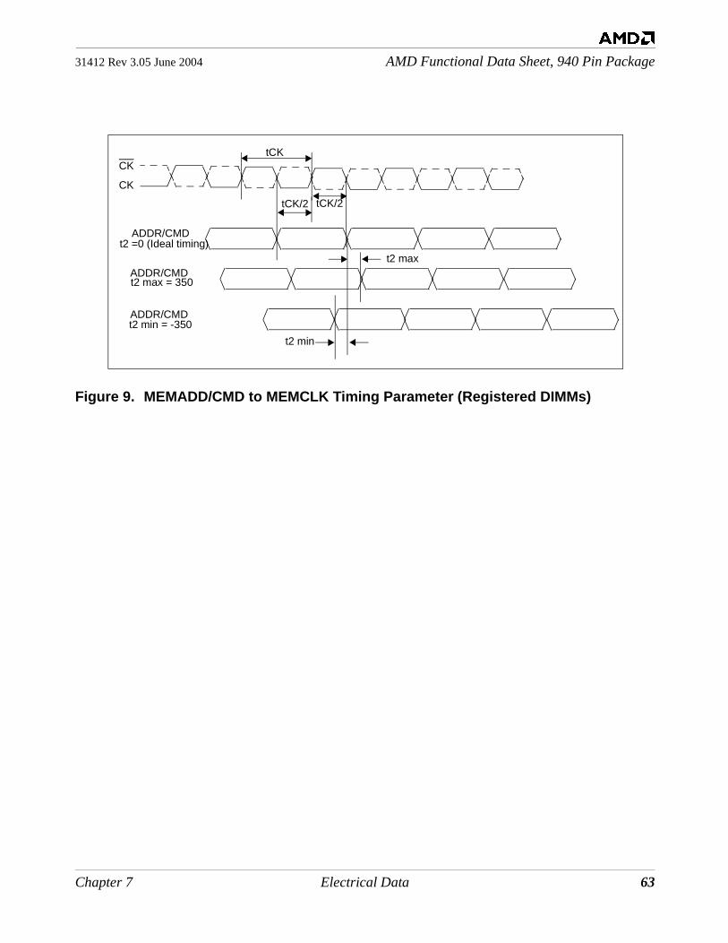
31412 Rev 3.05 June 2004 AMD Functional Data Sheet, 940 Pin Package
Figure 9. MEMADD/CMD to MEMCLK Timing Parameter (Registered DIMMs)
CK
CK
tCK
t2 =0 (Ideal timing)ADDR/CMD
ADDR/CMD
ADDR/CMD
tCK/2
t2 max = 350
t2 max
t2 min
tCK/2
t2 min = -350
Chapter 7 Electrical Data 63

AMD Functional Data Sheet, 940 Pin Package 31412 Rev 3.05 June 2004
Figure 10.MEMDQS Edge Arrival Relative to DQs
DQS
DQs Perfect
Edge Aligned
t3 = 0 ps
DQs Late arrival
from strobe
t3 Max
DQs Early
arrival from
strobe
t3 Min
t3 Max
t3 Min
setup
Package + PDL + Receiver uncertainty
64 Electrical Data Chapter 7

31412 Rev 3.05 June 2004 AMD Functional Data Sheet, 940 Pin Package
7.4 Clock Pins
7.4.1 Operating Conditions
Notes:1. VOD is the differential output voltage or the voltage difference between true and complement under DC or AC
conditions.2. DeltaVOD is the change in magnitude between the differential output voltage while driving logic 0 and while driving
logic 1.3. VOCM is the output common mode voltage defined as the average of the true voltage magnitude and the complement
voltage relative to ground under DC or AC conditions. 4. DeltaVOCM is the change in magnitude between the output common mode voltage while driving logic 0 and while
driving logic 1 under DC or AC conditions.
Table 26. DC Operating Conditions for CLKIN_H/L and FBCLKOUT_H/L Pins
Symbol Parameters Unit Min Typ Max Notes
VID Differential Input Voltage mV 300 2400
DeltaVID Change in VID Magnitude mV –50 50
VICM Input Common Mode Voltage mV VTT–100 VTT VTT+100
DeltaVICM Change in VICM Magnitude mV –50 50
VOD Differential Output Voltage V 1.2 1.3 1.4 1
DeltaVOD Change in VOD Magnitude mV –50 50 2
VOCM Output Common Mode Voltage V 1.1 1.25 1.4 3
DeltaVOCM Change in VOCM Magnitude mV –50 50 4
Chapter 7 Electrical Data 65

AMD Functional Data Sheet, 940 Pin Package 31412 Rev 3.05 June 2004
Notes:1. VOD is the differential output voltage or the voltage difference between true and complement under DC or AC
conditions.2. Delta VOD is the change in magnitude between the differential output voltage while driving logic 0 and while driving
logic 1.3. VOCM is the output common mode voltage defined as the average of the true voltage magnitude and the complement
voltage relative to ground under DC or AC conditions. 4. Delta VOCM is the change in magnitude between the output common mode voltage while driving logic 0 and while
driving logic 1 under DC or AC conditions.5. Measured differentially through the range of VICM – 400 mV to VICM + 400 mV.6. Spread spectrum clocking is limited to –0.5% downspread under normal operation.7. Measured at the differential crossing point. Maximum difference of cycle time between two adjacent cycles.
Table 27. AC Operating Conditions for CLKIN_H/L and FBCLKOUT_H/L Pins
Symbol Parameter Unit Min Typ Max Notes
F (PLL mode, VDDA=2.5 V)
Input Frequency Range (SSC) MHz 198.8 200 6
TJC Jitter, Cycle-to-Cycle pS 0 200 7
DC Input Duty Cycle (CLKIN_H/L) % 30 70
VBIAS Input BIAS Voltage Node mV VTT VTT VTT
VID Differential Input Voltage mV 400 2300
DeltaVID Change in VID Magnitude mV –150 150
VICM Input Common Mode Voltage mV VBIAS–200 VBIAS+200
DeltaVICM Change in VICM Magnitude mV –200 200
VOD Differential Output Voltage V 1.2 1.3 1.4 1
DeltaVOD Change in VOD Magnitude mV –100 100 2
VOCM Output Common Mode Voltage V 1.1 1.25 1.4 3
DeltaVOCM Change in VOCM Magnitude mV –100 100 4
IF Input Falling Edge Rate V/ns 1.2 10 5
IR Input Rising Edge Rate V/ns 1.2 10 5
CIN Input Capacitance pF 0 5
66 Electrical Data Chapter 7
31412 Rev 3.05 June 2004 AMD Functional Data Sheet, 940 Pin Package
7.5 Power-Up Signal SequencingFigure 12 on page 70 illustrates the signal sequencing requirements during a cold reset (power-up conditions). The HyperTransport™ link reset sequencing is defined in the HyperTransport™ I/O Link Specification.
The following list describes the power-up signal sequencing illustrated in Figure 12. Note that the numbered items correspond to the numbers in Figure 12.
1. RESET_L must be asserted a minimum of 1ms prior to the assertion of PWROK, as defined in theHyperTransport™ I/O Link Specification. The TMS pin must be asserted a minimum of 10nsbefore PWROK assertion and must be held in the High state a minimum of 10ns after theassertion of PWROK.
2. CLKIN_H/L must be within specification at the time the VDD power supply begins to ramp.
3. PWROK remains deasserted at least 1ms after CLKIN_H/L is stable and voltages to the processorare within specification. The processor determines if there are devices attached to itsHyperTransport™ links 10µs after the assertion of PWROK.
4. After PWROK assertion, the VID[4:0] signals change from the metal mask VID[4:0]* to thevalue programmed during device manufacturing. The PLL begins locking to the frequencyprogrammed during device manufacturing 160µs after PWROK is asserted.
5. LDTSTOP_L must be deasserted a minimum of 1µs before the deassertion of RESET_L, asdefined by the HyperTransport™ I/O Link Specification.
6. The RESET_L signal remains asserted a minimum of 1mS after PWROK assertion, as defined inthe HyperTransport™ I/O Link Specification. The clocks from the transmitters of allHyperTransport™ technology devices must be stable before RESET_L is deasserted.
7. The MEMCLK_LO_H/L[3:0] and MEMCLK_UP_H/L[3:0] signals are stable after BIOS sets theMemory Clock Ratio Valid (MCR) bit in the processor’s DRAM Config Upper register. TheMEMCLK* period is defined by the MEMCLK[2:0] field in the DRAM Config Upper register.
8. MEMRESET_L is deasserted after BIOS sets the Dram_Init bit in the DRAM Config Lowerregister. This allows time for the PLL on registered DIMMs to stabilize before the deassertion ofthe DIMM’s reset signal. The delay between these events depends on the silicon revision and theDRAM operating speed as described in Figure 11 and Table 29 on page 68.
9. The MEMCKE_LO/UP signals are asserted following the deassertion of MEMRESET_L. Thedelay between these events depends on the silicon revision and the DRAM operating speed asdescribed in Figure 11 and Table 29 on page 68. Note that the MEMCKE_LO/UP delay fromMEMRESET_L is different when exiting self-refresh as listed in Table 30 on page 69.
* The metal mask VID[4:0] is the value driven on the VID[4:0] lines prior to PWROK assertion. Refer to Table 28 for metal mask VID[4:0] values.
Chapter 7 Electrical Data 67
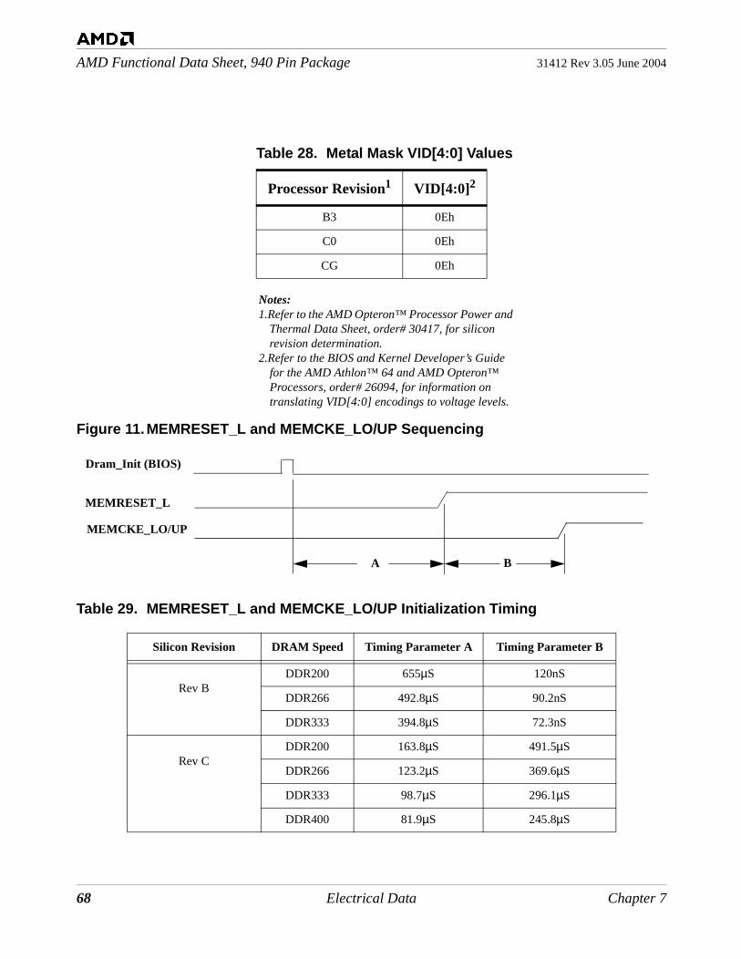
AMD Functional Data Sheet, 940 Pin Package 31412 Rev 3.05 June 2004
Notes:1.Refer to the AMD Opteron™ Processor Power and
Thermal Data Sheet, order# 30417, for silicon revision determination.
2.Refer to the BIOS and Kernel Developer’s Guide for the AMD Athlon™ 64 and AMD Opteron™ Processors, order# 26094, for information on translating VID[4:0] encodings to voltage levels.
Figure 11.MEMRESET_L and MEMCKE_LO/UP Sequencing
Table 29. MEMRESET_L and MEMCKE_LO/UP Initialization Timing
Table 28. Metal Mask VID[4:0] Values
Processor Revision1 VID[4:0]2
B3 0Eh
C0 0Eh
CG 0Eh
Silicon Revision DRAM Speed Timing Parameter A Timing Parameter B
Rev BDDR200 655µS 120nS
DDR266 492.8µS 90.2nS
DDR333 394.8µS 72.3nS
Rev CDDR200 163.8µS 491.5µS
DDR266 123.2µS 369.6µS
DDR333 98.7µS 296.1µS
DDR400 81.9µS 245.8µS
Dram_Init (BIOS)
MEMRESET_L
MEMCKE_LO/UP
A B
68 Electrical Data Chapter 7

31412 Rev 3.05 June 2004 AMD Functional Data Sheet, 940 Pin Package
Table 30. MEMCKE_LO/UP Delay from MEMRESET_L During Exit from Self-Refresh
Note: Refer to the AMD Opteron™ Processor Power and Thermal Data Sheet, order# 30417, for silicon revision determination.
Silicon Revision DRAM Speed Registered DIMMs
Rev BDDR200 120nS
DDR266 90.2nS
DDR333 72.2nS
Rev CDDR200 10.24µS
DDR266 7.6µS
DDR333 6.1µS
DDR400 5.1µS
Chapter 7 Electrical Data 69

AMD Functional Data Sheet, 940 Pin Package 31412 Rev 3.05 June 2004
Figure 12.Power-Up Signal Sequencing
PWROK
RESET_L
MEMRESET_L
VID[4:0]
MEMCKE*
CLKIN_H/L
MEMCLK*
(Metal Mask VID[4:0])
VALID
VDD
1
3
6
7
4
8
2
LDTSTOP_L
5
L0_CLKIN_H/L[1:0]
TMS
9
70 Electrical Data Chapter 7

31412 Rev 3.05 June 2004 AMD Functional Data Sheet, 940 Pin Package
7.6 Reference Information
Notes:1. CLKIN_H/L inputs have DC voltage BIAS generating circuits on the inputs. These consist of both a ~250-ohm pullup
resistor to VTT on each input and a ~250-ohm series input resistor.2. Refer to Table 6 on page 41 for definitions in pin Type column.3. Systems that do not require use of these pins can rely on the internal termination to pull the signals to the proper
inactive state. When these pins are used they must not be driven with open-drain outputs or additional termination is required.
Table 31. Internal Termination for Miscellaneous Pins Interface
Pin Type2 Internal Termination Value Tolerance
CLKIN_H/L I-IOD None1
FBCLKOUT_H/L O-IOD 80-ohm differential termination ±50%
RESET_L I-IOS None
PWROK I-IOS None
VID[4:0] O-IOS None
LDTSTOP_L I-IOS None
THERMDA A None
THERMDC A None
THERMTRIP_L O-IO-OD None
COREFB_H/L A None
TCK I-IOS Pullup to VDDIO3 533 ohms ±50%
TMS I-IOS Pullup to VDDIO3 533 ohms ±50%
TRST_L I-IOS Pullup to VDDIO3 533 ohms ±50%
TDI I-IOS Pullup to VDDIO3 533 ohms ±50%
TDO O-IOS Pullup to VDDIO 533 ohms ±50%
DBREQ_L I-IOS Pullup to VDDIO3 533 ohms ±50%
DBRDY O-IOS Pullup to VDDIO 533 ohms ±50%
Chapter 7 Electrical Data 71

AMD Functional Data Sheet, 940 Pin Package 31412 Rev 3.05 June 2004
Notes:1. See the AMD Athlon™ 64 FX and AMD Opteron™ Processor Motherboard Design Guide, order# 25180, for proper
resistor values.2. Input pins of the same type may be pulled high or low through a shared resistor provided that VIL Max and VIH Min
specifications are not exceeded for those pin types.
Table 32. External Required Circuits (Pins Not Normally Used in System)
Pin External Circuit (Non-Operating)1
NC_G14 Tied to VDDIO_SUS through resistor
NC_H14 Tied to VSS through resistor
NC_AE14 Tied to VDDIO_RUN through resistor
NC_AF13 Tied to VDDIO_RUN through resistor
NC_AE10 Tied to VSS through resistor
NC_AE11 Tied to VSS through resistor
NC_AF11 Tied to VSS through resistor
NC_AE13 Tied to VSS through resistor
NC_AE12 Tied to VSS through resistor
NC_T3 Tied to VSS through resistor
NC_T4 Tied to VLDT through resistor
72 Electrical Data Chapter 7

31412 Rev 3.05 June 2004 AMD Functional Data Sheet, 940 Pin Package
7.7 Thermal Diode SpecificationsAn on-die thermal diode is provided as a tool for thermal management. An external sensor is necessary to measure the temperature of the thermal diode.
Thermal solutions should be not designed and validated using the thermal diode. Thermal solutions should be designed and validated against the case temperature specification per the methodology specified in AMD Athlon™ 64 and AMD Opteron™ Processors Thermal Design Guide, order# 26633.
Table 33. Thermal Diode Specification Revision and Frequency Guide
Note: Refer to the AMD Opteron™ Processor Power and Thermal Data Sheet, order# 30417 for silicon revi-sion determination.
Notes:1. The sourcing current should always be used in forward bias. 2. Characterized at 95ºC with a forward bias current pair of 10 and 100 µA. The ideality factor limits correspond to the
diode offset limits.3. Temperature offset is unique for each processor. The diode offset value is found in the Thermtrip Status Register
discussed in the BIOS and Kernel Developer’s Guide for the AMD Athlon™ 64 and AMD Opteron™ Processors, order# 26094.
4. This diode offset supports temperature sensors using two sourcing currents only. Other sourcing current implementations are not supported by AMD.
5. The temperature offset is set based on a sourcing current pair of 10 and 100 µA and an ideality factor of 1.008. The diode offset should be subtracted from the temperature sensor reading. If the temperature sensor has an ideality factor different from 1.008, an additional offset is needed. Contact your temperature sensor vendor about whether an additional offset is needed.
6. After correcting for the diode offset, the thermal diode has an accuracy of ±10°C. This accuracy is additive to the temperature sensor accuracy.
Rev/Freq < 2.2GHz >= 2.2GHz
B3 Table 34 N/A
C0 Table 34 Table 35
CG and later Table 35 Table 35
Table 34. Thermal Diode Specifications (Revision and Frequency Dependent, see Table 33)
Symbol Parameter Units Min Typ Max Notes
I Sourcing Currents µA 5 500 1
nf Ideality Factor 1.008 1.096 2
TOffset Temperature Offset °C 0 32 3, 4, 5, 6
θj-c Thermal resistance (junction to case) °C/W 0.32 7
Chapter 7 Electrical Data 73

AMD Functional Data Sheet, 940 Pin Package 31412 Rev 3.05 June 2004
7. The temperature specification for the processor is based on the case temperature. The thermal resistance from the junction to the case is provided as a reference for implementing fan-speed control using the thermal diode.
Table 35. Thermal Diode Specifications (Revision and Frequency Dependent, see Table 33)
Notes:1. The sourcing current should always be used in forward bias.2. The temperature offset is used to normalize the thermal diode measurement to reflect case temperature at the worst
case conditions for a part.3. This diode offset supports temperature sensors using two sourcing currents only. Single sourcing current
implementations are not supported by AMD.4. The temperature offset is unique for each processor and is programmed at the factory. The diode offset value is found
in the Thermtrip Status Register described in the BIOS and Kernel Developer’s Guide for the AMD Athlon™ 64 and AMD Opteron™ Processors, order# 26094.
5. TOffset should be subtracted from the temperature sensor reading. If the temperature sensor has an ideality factor
different from 1.008, a small correction to this offset is required. Contact your temperature sensor vendor to determine if additional correction is required.
Symbol Parameter Units Min Typ Max Notes
I Sourcing Currents µA 5 500 1
TOffset Temperature Offset °C 0 52 2, 3, 4, 5
74 Electrical Data Chapter 7

31412 Rev 3.05 June 2004 AMD Functional Data Sheet, 940 Pin Package
7.8 Power Supplies
7.8.1 Operating Conditions
Table 36. Combined AC and DC Operating Conditions for Power Supplies
Symbol Parameter Unit Min Typ Max Notes
VID_VDD VID Requested VDD Supply Level V See Note 11 6
VDD_dc VDD Supply Voltage V VID_VDD–50 mV
VID_VDD VID_VDD+50 mV
VDD_ac VDD Supply Voltage V VID_VDD–100 mV
VID_VDD+100 mV
13
VDD_PON VDD Supply Voltage before PWROK assertion during power-on.
V 1.15 1.20 VDD_max 8
VDDIO_dc VDDIO Supply Voltage for DDR333 and below
V 2.40 2.50 2.60 10
VDDIO_dc VDDIO Supply Voltage for DDR400 and below
V 2.50 2.60 2.65 10, 12
VDDIO_ac VDDIO supply voltage V VDDIO_dc-150 mV
VDDIO_dc+150 mV
9
VLDT VLDT Supply Voltage V 1.14 1.20 1.26
VTT_dc VTT Supply Voltage V VDDIO_dc Min/2 - 50 mV
VDDIO_dc Typ/2
VDDIO_dc Max/2 + 50 mV
VTT_ac VTT Supply Voltage V VTT_dc- 150 mV
VTT_dc+ 150 mV
9
VDDA VDDA Supply Voltage V 2.40 2.50 2.60
IDD VDD Power Supply Current A See Note 11
IDDIO1 VDDIO Power Supply Current A 2.8 2.9 4
IDDIO2 VDDIO Power Supply Current in S3 State
mA 850
ITT1 VTT Power Supply Current mA 200 2, 5
ITT2 VTT Power Supply Current in S3 State mA 200
ILDT VLDT Power Supply Current A 1.5 1
IDDA VDDA Power Supply Current mA 33
IDDslew1 VDD Power Supply Current Change During Normal Operation
A/µs .0583*fMHz 3, 7
IDDslew2 VDD Power Supply Current Change Upon Reset Exit
A/µs 270 3
IDDslew3 VDD Power Supply Current Change Upon Stop Grant Entry
A/µs –270 3
Chapter 7 Electrical Data 75

AMD Functional Data Sheet, 940 Pin Package 31412 Rev 3.05 June 2004
Notes:1. ILDT is specified for three 16x16-bit HyperTransport™ links operating at 1.6 GT/s.2. VTT must both sink and source current.3. Current slew rates are controlled by ramping up or down the core frequency in steps during these sequences to control
in-rush currents.4. VDDIO current is consumed by I, O, I/O switching current and on-chip functions (PDL, DLL, level-shifters, etc.).5. VTT current is consumed by I, O, I/O switching current and on-chip functions (PDL, DLL, level-shifters, etc.).6. The processor drives a VID code corresponding to this voltage. 7. For example, the IDDslew1 calculation for a 1.2-GHz part is (.0583 x 1200) = 69.96 A/µs.8. The processor’s VID[4:0] outputs select VID_PON nom before PWROK is asserted. Transients up to VDD_max are
allowed.9. VDDIO_ac and VTT_ac parameters are measured +/- 1ns of all data bus bits switching.10. Systems designed to DDR400 power supply parameters will also operate correctly with DDR333 and below.11. Refer to the AMD Opteron™ Processor Power and Thermal Data Sheet, order# 30417, for these specifications.12. DDR400 (200MHz) supported by Rev C0 and later. Refer to the AMD Opteron™ Processor Power and Thermal
Data Sheet, order# 30417 for silicon revision determination.13. Transient duration below VDD_dc min is limited to < 5µs. Transient duration above VDD_dc max is limited to < 2%
duty cycle. Test by probing differentially at COREFB_H and COREFB_L with 20MHz scope bandwidth limit. Test conditions are while running AMD’s MAXPOWER64 utility using AMD thermal approved production grade heat sinks in normal room ambient conditions.
7.8.2 Thermal Power
Refer to AMD Opteron™ Processor Power and Thermal Data Sheet, order# 30417, for thermal power specifications.
7.8.3 Power Supply Relationships
7.8.3.1 Sequencing Relationships
Power supply relationships during power-up, power-down, and entry and exit of any power management state must be controlled in order to avoid damage to the device and help ensure proper operation of the device. Figure 13 shows an example of how these relationships can be maintained by system power generation and distribution schemes. PWROK must be deasserted as VDD decays during power down. VTT and VDDIO are considered SUSPEND planes and are powered in the S0 (working) state and the S1 and S3 sleep states. VDDA, VDD, and VLDT are considered RUN planes and are powered in the S0 and S1 states only. All power supplies should be turned off during the S4 (SUSPEND to DISK) and S5 (SOFT-OFF) states. VDDIO (RUN) is a power rail used for pull-ups on
IDDslew4 VDD Power Supply Current Change Upon Stop Grant Exit
A/µs 270 3
IDDslew5 VDD Power Supply Current Change Upon Non-reset Power Failure
A/µs –4.25 3
Table 36. Combined AC and DC Operating Conditions for Power Supplies
Symbol Parameter Unit Min Typ Max Notes
76 Electrical Data Chapter 7
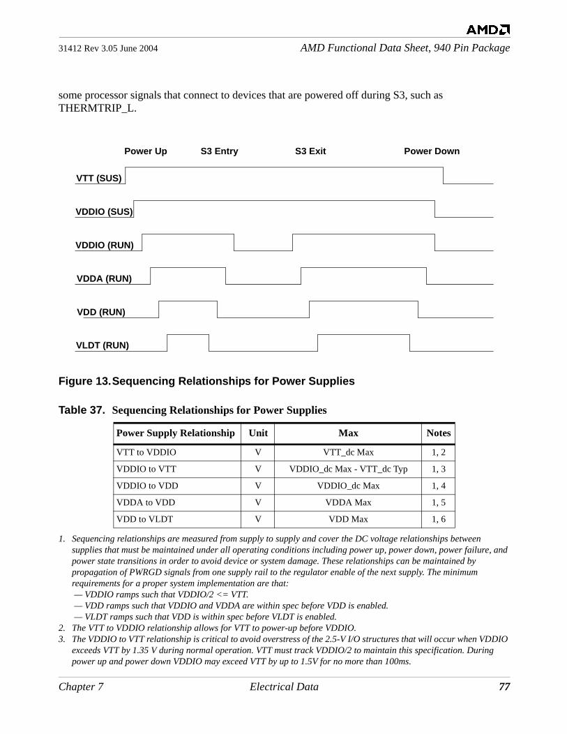
31412 Rev 3.05 June 2004 AMD Functional Data Sheet, 940 Pin Package
some processor signals that connect to devices that are powered off during S3, such as THERMTRIP_L.
Figure 13.Sequencing Relationships for Power Supplies
Table 37. Sequencing Relationships for Power Supplies
1. Sequencing relationships are measured from supply to supply and cover the DC voltage relationships between supplies that must be maintained under all operating conditions including power up, power down, power failure, and power state transitions in order to avoid device or system damage. These relationships can be maintained by propagation of PWRGD signals from one supply rail to the regulator enable of the next supply. The minimum requirements for a proper system implementation are that: — VDDIO ramps such that VDDIO/2 <= VTT. — VDD ramps such that VDDIO and VDDA are within spec before VDD is enabled. — VLDT ramps such that VDD is within spec before VLDT is enabled.
2. The VTT to VDDIO relationship allows for VTT to power-up before VDDIO.3. The VDDIO to VTT relationship is critical to avoid overstress of the 2.5-V I/O structures that will occur when VDDIO
exceeds VTT by 1.35 V during normal operation. VTT must track VDDIO/2 to maintain this specification. During power up and power down VDDIO may exceed VTT by up to 1.5V for no more than 100ms.
Power Supply Relationship Unit Max Notes
VTT to VDDIO V VTT_dc Max 1, 2
VDDIO to VTT V VDDIO_dc Max - VTT_dc Typ 1, 3
VDDIO to VDD V VDDIO_dc Max 1, 4
VDDA to VDD V VDDA Max 1, 5
VDD to VLDT V VDD Max 1, 6
VTT (SUS)
VDDIO (SUS)
VDDIO (RUN)
VDDA (RUN)
VDD (RUN)
VLDT (RUN)
Power Up S3 Entry S3 Exit Power Down
Chapter 7 Electrical Data 77

AMD Functional Data Sheet, 940 Pin Package 31412 Rev 3.05 June 2004
4. The VDDIO to VDD relationship allows for VDDIO to power-up before VDD.5. The VDDA to VDD relationship allows for VDDA to power-up before VDD. VDDA must power-up before VDD to
ensure that internal clock sources are valid before being used and that clock source multiplexors are properly controlled.
6. The VDD to VLDT relationship allows for VDD to power-up before VLDT and specifically allows for VDD=VDD_max with VLDT=0 V. VDD must power-up before VLDT to help ensure that PWROK is properly passed from the pins into the VDD power domain such that the deasserted state can be seen in the VLDT power domain.
7.8.3.2 Sequencing Relationships: Signals to Power Supplies (Stress Conditions)
Once the powerup sequence has been completed and PWROK can be asserted, the sequencing ofinput signals to the CPU and output signals from the CPU can begin. The requirements from signalsto power supplies are summarized by type as follows.
• VDDIO inputs and outputs are allowed to exceed VDDIO by 0.3V and are allowed to be 0.3V below VSS.
• VDDIO inputs are allowed to exceed VTT by VTT_dc Max + 0.3V and are allowed to be 0.3V below VSS.
• VLDT inputs and outputs are allowed to exceed VLDT by 0.3V and are allowed to be 0.3V below VSS.
7.8.3.3 Power Failures
The power sequencing relationships defined in sections 7.8.3.1 and 7.8.3.2 must be guaranteed by the motherboard power supply subsystem in the event of a power failure.
7.8.3.4 Power States
During system power state S3, the RUN supplies (VLDT, VDD, and VDDA) to the CPU are to be turned off. During this operating mode, all internal leakage paths between SUS supplies (VDDIO and VTT) and these powered off planes are disabled. During S0 and S1, all RUN and SUS planes are to be powered on. During S4 and S5, all supplies to the CPU are to be turned off.
7.8.3.5 Unused Links
Because the processor has up to three independent HyperTransport™ links, some implementations will not connect one or more of these links. In this case, the VLDT of the link that is not connected to another device, should be connected to the VLDT of an operating link. Note that even if the link is not used, the VLDT for the link must be connected so that the internal link detection circuitry can successfully determine the connection status of the link.
78 Electrical Data Chapter 7

31412 Rev 3.05 June 2004 AMD Functional Data Sheet, 940 Pin Package
8 Package Specifications
8.1 Mechanical Loading for Lidded PartsTable 38 provides the mechanical loading specification for lidded parts. These specifications shouldnot be exceeded during heat sink installation, system testing, or system shipment. Refer to the AMDAthlon™ 64 and AMD Opteron™ Processors Thermal Design Guide, order# 26633, for moreinformation on properly designing a heat sink to meet these specifications.
Notes:1.Load specified for coplanar, uniform contact to lid surface.2.The static specification specifies the allowable range to be applied by the heat sink to the processor package.3.The dynamic specification assumes a dynamic load that includes the static load and is applied at 50G for 11ms
Table 38. Mechanical Loading for Lidded Parts
Type UnitsMaximum
ForceNotes
Static lbf 100 1, 2
Dynamic lbf 200 1, 3
Chapter 8 Package Specifications 79

AMD Functional Data Sheet, 940 Pin Package 31412 Rev 3.05 June 2004
8.2 Package Diagram
Figure 14. Ceramic Micro Pin Grid Array Package: Top, Side, and Bottom Views
D1/E1
D2/E2
SYMBOL
PACKAGE
WT (gms)
BOTTOM VIEW
LID
SIDE VIEW
TOP VIEW
handling and orientation purposes. package that identifies the pin A1 corner and can be used for 3. This corner has a chamfer and a square on top of the
1. All dimensions are specified in millimeters (mm).
4. Pin tips should have radius.
2. Dimensioning and tolerancing per ASME-Y14.5M-1994.
5. Symbol "M" defines the pin matrix size and "N" is number of pins.
0.25
0.50
B
E
GENERAL NOTES
C
L
NxØb
A2
E2
NOT TO SCALE
A1
CM
M C A B
K 4
A
ccc
DETAIL K
R
b1
A1 CORNER
3
D2
D A
D1
0.81 1.06
0.30 MAX
2.29
45.17 REF
N
ccc
R
M
b1
L
940
0.125
2.03
31
max.
1.27 BSC
0.35
40.20
4.88 REF
38.10 BSC
1.796
3.35
VARIATIONS
xUCG940
37.6
A1
e
b
A2
A
1.556
0.275
3.05
37.4
D/E
AMD
39.80
min.
Øb1
(Nx Plcs)
e
SEE NOTES
E1
5
A1 CORNER
80 Package Specifications Chapter 8