Embed Size (px)
Citation preview

RESET
SHTDWN
A3
SCL
SDAI
AINAGND DGND
KSENSx
INT
SDAO
AOUT
DRAINn
GATEn
VDD VPWR
SENn22
100 nF100 V
47
255 m
Note: only port n shown
TPS23861
PORTn
48 V3.3 V
Copyright © 2016, Texas Instruments Incorporated
TOP CONDUCTORS
BOTTOM GND PLANEContinuous, Robust Backside GND Plane
FETs Uniformly Spread Over Surface
Product
Folder
Order
Now
Technical
Documents
Tools &
Software
Support &Community
An IMPORTANT NOTICE at the end of this data sheet addresses availability, warranty, changes, use in safety-critical applications,intellectual property matters and other important disclaimers. PRODUCTION DATA.
TPS23861SLUSBX9H –MARCH 2014–REVISED NOVEMBER 2017
TPS23861 IEEE 802.3at Quad Port Power-over-Ethernet PSE Controller
1
1 Features1• IEEE 802.3at Quad Port PSE Controller
– Auto Detect, Classification– Auto Turn-On and Disconnect– Efficient 255-mΩ Sense Resistor
• Pin-Out Enables Two-Layer PCB• Kelvin Current Sensing• 4-Point Detection• Automatic Mode – As Shipped
– No External Terminal Setting Required– No Initial I2C Communication Required
• Semi-Automatic Mode – Set by I2C Command– Continuous Identification and Classification– Meets IEEE 400-ms TPON Specification– Fast-Port Shutdown Input– Operates best when used in conjunction with
system reference codehttp://www.ti.com/product/TPS23861/toolssoftware
• Optional I2C Control and Monitoring• –40°C to 125°C Temperature Range• TSSOP 28 Package 9.8 mm x 6.6 mm
2 Applications• Ethernet Switches and Routers• Surveillance NVR and DVRs• Residential Gateways• PoE Pass-Through Systems• Wireless Backhaul
3 DescriptionThe TPS23861 is an easy-to-use, flexible,IEEE802.3at PSE solution. As shipped, itautomatically manages four 802.3at ports without theneed for any external control.
The TPS23861 automatically detects PoweredDevices (PDs) that have a valid signature, determinespower requirements according to classification andapplies power. Two-event classification is supportedfor type-2 PDs. The TPS23861 supports DCdisconnection and the external FET architectureallows designers to balance size, efficiency andsolution cost requirements.
The unique pin-out enables 2-layer PCB designs vialogical grouping and clear upper and lowerdifferentiation of I2C and power pins. This deliversbest-in-class thermal performance, Kelvin accuracyand low-build cost.
In addition to automatic operation, the TPS23861supports Semi-Auto Mode via I2C control for precisionmonitoring and intelligent power management.Compliance with the 400-ms TPON specification isensured whether in semi-automatic or automaticmode.
Device InformationPART NUMBER PACKAGE BODY SIZE
TPS23861 TSSOP (28) 9.80 mm x 6.60 mm
Simplified Schematic

2
TPS23861SLUSBX9H –MARCH 2014–REVISED NOVEMBER 2017 www.ti.com
Product Folder Links: TPS23861
Submit Documentation Feedback Copyright © 2014–2017, Texas Instruments Incorporated
Table of Contents1 Features .................................................................. 12 Applications ........................................................... 13 Description ............................................................. 14 Revision History..................................................... 25 Pin Configuration and Functions ......................... 56 Specifications......................................................... 6
6.1 Absolute Maximum Ratings ...................................... 66.2 ESD Ratings.............................................................. 66.3 Recommended Operating Conditions....................... 66.4 Thermal Information .................................................. 66.5 Electrical Characteristics........................................... 76.6 Timing Requirements .............................................. 116.7 Switching Characteristics ........................................ 126.8 Typical Characteristics ............................................ 16
7 Detailed Description ............................................ 217.1 Overview ................................................................. 217.2 Functional Block Diagram ....................................... 257.3 Feature Description................................................. 257.4 Device Functional Modes........................................ 407.5 Register Map – I2C-Addressable ............................ 45
8 Application and Implementation ........................ 85
8.1 Introduction to PoE ................................................. 858.2 Application Information............................................ 858.3 Typical Application .................................................. 878.4 System Examples ................................................... 93
9 Power Supply Recommendations ...................... 979.1 VDD......................................................................... 979.2 VPWR ..................................................................... 979.3 VPWR-RESET Sequencing .................................... 97
10 Layout................................................................... 9810.1 Layout Guidelines ................................................. 9810.2 Layout Example .................................................... 99
11 Device and Documentation Support ............... 10011.1 Documentation Support ..................................... 10011.2 Receiving Notification of Documentation
Updates.................................................................. 10011.3 Community Resources........................................ 10011.4 Trademarks ......................................................... 10011.5 Electrostatic Discharge Caution.......................... 10011.6 Glossary .............................................................. 100
12 Mechanical, Packaging, and OrderableInformation ......................................................... 101
4 Revision HistoryNOTE: Page numbers for previous revisions may differ from page numbers in the current version.
Changes from Revision G (October 2016) to Revision H Page
• Deleted "or unknown" from Auto subsection ........................................................................................................................ 42• Deleted "and Auto Modes" from TSTART Indicators of Detect and Class Failures subsection........................................... 44• Changed fault conditions for Auto mode in Detect and Class Failure Indicators table ........................................................ 44• Added information to Step 2 in Start/ILIM Event Register subsection ................................................................................. 53
Changes from Revision F (July 2016) to Revision G Page
• Deleted the MAX value of 150 mA from IGO- in the Electrical Characteristics ........................................................................ 8
Changes from Revision E (March 2016) to Revision F Page
• Legacy Device Detection, Changed the paragraph, "in general,..." ..................................................................................... 30• Changed section From: Independent Operation when the Bit is Set To: Independent Operation when the AUTO Bit
is Set..................................................................................................................................................................................... 34• I2C Slave Address and AUTO Bit Programming, Added NOTE: "When using I2C scan...".................................................. 37• Start/ILIM Event Register, Changed the third list item From: "Detect fault or classification unknown,.." To:
"Overcurrent or class mismatch on second finger in Semi-Auto or Manual Mode." ........................................................... 53• Timing Configuration Register, Added new NOTE under TLIM[1:0]: " If ILIM and ICUT are set to same value..." ............ 61• Timing Configuration Register, Added new NOTE under TICUT[1:0]: " If ILIM and ICUT are set to same value..." .......... 62• Two-Event Classification Register, Changed the second list item to include: "CLEn is set or a" ....................................... 67• Replaced Figure 58 .............................................................................................................................................................. 95

3
TPS23861www.ti.com SLUSBX9H –MARCH 2014–REVISED NOVEMBER 2017
Product Folder Links: TPS23861
Submit Documentation FeedbackCopyright © 2014–2017, Texas Instruments Incorporated
Changes from Revision D (September 2015) to Revision E Page
• Added note in Features, "Semi-Automatic Mode " ................................................................................................................. 1• Updated Pin Functions table .................................................................................................................................................. 5• Added new Figure 37 .......................................................................................................................................................... 22• Added new Functional Block Diagram.................................................................................................................................. 25• Changed note in A/D Converter and I2C Interface .............................................................................................................. 32• Changed the Note in I2C Slave Address and AUTO Bit Programming ................................................................................ 35• Added note to I2C Slave Address and AUTO Bit Programming .......................................................................................... 35• Changed I2C slave address register note............................................................................................................................. 35• Added new Figure 43 ........................................................................................................................................................... 39• Added a note to Manual about type 2 power 2 event classification. .................................................................................... 40• Added content to Semi-Auto................................................................................................................................................. 41• Added "PoEPn" column to Bits Description.......................................................................................................................... 70• Added a note to PoE Plus Register ..................................................................................................................................... 77
Changes from Revision C (June 2015) to Revision D Page
• Added reference note to Figure 5 and Figure 6 ................................................................................................................... 15• Changed RESET note to add addition reference link. ........................................................................................................ 23• Added SDAO pin note. ........................................................................................................................................................ 24• Changed I2C Slave Address and AUTO Bit Programming note. ......................................................................................... 35• Added Figure 42, I2C/SMBus Interface Slave Address Programming Protocol. ................................................................. 38• Added note 3 to Table 10 ..................................................................................................................................................... 45• Changed Connections on Unused Ports section.................................................................................................................. 86• Added reference link to the VPWR-RESET Sequencing note. ............................................................................................ 97
Changes from Revision B (April 2015) to Revision C Page
• Added Figure 5 and Figure 6................................................................................................................................................ 15• Changed Figure 36, Disconnected AIN pin from GND......................................................................................................... 22• Added SHTDWN note. ......................................................................................................................................................... 23• Added RESET note. ............................................................................................................................................................ 23• Added Device Power On Initialization section...................................................................................................................... 44• Added note 2 to Table 10 ..................................................................................................................................................... 45• Added Port n Status Register note....................................................................................................................................... 55• Added Operating Mode Register Command note. .............................................................................................................. 58• Added Operating Mode Register Bit Description note. ........................................................................................................ 58• Added Detect/Class Enable Register Command note. ....................................................................................................... 59• Added Detect/Class Restart Register Command note. ........................................................................................................ 64• Added Power Enable Register Command note.................................................................................................................... 65• Added Power Enable Register Bit Descriptions note. .......................................................................................................... 65• Added Reset Register Command note................................................................................................................................. 66• Added Reset Register Bit Descriptions note. ...................................................................................................................... 66• Changed Figure 46, Disconnected AIN pin from GND......................................................................................................... 85• Changed Figure 48, Disconnected AIN pin from GND......................................................................................................... 87• Changed Figure 49, Disconnected AIN pin from GND......................................................................................................... 88• Changed Figure 50, Disconnected AIN pin from GND......................................................................................................... 89

4
TPS23861SLUSBX9H –MARCH 2014–REVISED NOVEMBER 2017 www.ti.com
Product Folder Links: TPS23861
Submit Documentation Feedback Copyright © 2014–2017, Texas Instruments Incorporated
• Changed QPn description in Per Port Components ............................................................................................................. 90• Changed maximum VDD supply current from 10 mA to 6 mA in first paragraph and changed wording in second
paragraph of VDD................................................................................................................................................................. 97• Added VPWR-RESET Sequencing ...................................................................................................................................... 97
Changes from Revision A (June, 2014) to Revision B Page
• Changed VDD current consumption from 10 mA (MAX) to 6.0 mA (MAX)............................................................................ 7• Deleted Processor watchdog trip delay specification. .......................................................................................................... 11• Added When using the I2C interface note. .......................................................................................................................... 32• Added When using the I2C interface note. .......................................................................................................................... 35• Changed FULL SCALE VALUE from 146.2°C to 150°C (typical). ....................................................................................... 71• Changed LSB VALUE from 0.652°C to 7°C......................................................................................................................... 71• Added Temperature sensor performance note..................................................................................................................... 71
Changes from Original (March 2014) to Revision A Page
• Added full TPS23861 IEEE 802.3at Quad Port Power-over-Ethernet PSE Controller datasheet. ........................................ 1

1
2
3
9
4
10
5
11
6
12
7
13
8
14
28
27
26
20
25
19
24
18
23
17
22
16
21
15
VDD
RESET
SCL
DRAIN3
SDAI
GATE3
SDAO
KSENSB
INT
SEN4
DGND
DRAIN4
SEN3
GATE4
VPWR
N/C
AOUT
DRAIN2
AIN
SEN2
SHTDWN
KSENSA
A3
GATE1
AGND
DRAIN1
GATE2
SEN1
5
TPS23861www.ti.com SLUSBX9H –MARCH 2014–REVISED NOVEMBER 2017
Product Folder Links: TPS23861
Submit Documentation FeedbackCopyright © 2014–2017, Texas Instruments Incorporated
5 Pin Configuration and Functions
PW Package28-Pin TSSOP
Top View
Pin FunctionsPIN
I/O DESCRIPTIONNAME NO.A3 23 I I2C A3 address line. Internally pulled up to VDD.AGND 22 P Analog ground.AIN 25 I I2C address programming input line; this pin is internally pulled up to VDD.AOUT 26 O I2C address programming line; this output is open drain.DGND 7 P Digital ground.DRAIN3 9 I
Port 1-4 output voltage monitor; connect to output port through a 47-Ω resistor.DRAIN4 13 IDRAIN1 16 IDRAIN2 20 IGATE3 10 O
Port 1-4 gate-drive output.GATE4 14 OGATE1 17 OGATE2 21 O
INT 6 O Interrupt; this pin asserts low when a bit in the interrupt register is asserted. This pin isupdated between I2C transactions. This output is open drain.
KSENSA 18 I Kelvin point connection for SEN1 and SEN2.KSENSB 11 I Kelvin point connection for SEN3 and SEN4.N/C 27 x Used to effect regulatory voltage-spacing compliance. Leave this pin open.RESET 2 I Reset; when asserted low, the device resets. This pin is internally pulled up to VDD.SCL 3 I Serial clock input for I2C bus.SDAI 4 I Serial data input for I2C bus; this pin can be connected to SDAO for non-isolated systems.
SDAO 5 O Serial data output for I2C bus; this pin can be connected to SDAI for non-isolated systems.This output is open drain.
SEN3 8 I
Port 1-4 current-sense input; connect to current-sense resistor through a 22-Ω resistor.SEN4 12 ISEN1 15 ISEN2 19 ISHTDWN 24 I Low-priority ports shutdown.VDD 1 P Digital 3.3-V supply. Bypass VDD to DGND using a 0.1-μF capacitor.VPWR 28 P Analog 48-V supply. Bypass VPWR to AGND using a 0.1-μF capacitor.

6
TPS23861SLUSBX9H –MARCH 2014–REVISED NOVEMBER 2017 www.ti.com
Product Folder Links: TPS23861
Submit Documentation Feedback Copyright © 2014–2017, Texas Instruments Incorporated
(1) Stresses beyond those listed under Absolute Maximum Ratings may cause permanent damage to the device. These are stress ratingsonly, which do not imply functional operation of the device at these or any other conditions beyond those indicated under RecommendedOperating Conditions. Exposure to absolute-maximum-rated conditions for extended periods may affect device reliability.
(2) Do not apply external voltage sources directly.(3) Application of voltage is not implied – these are internally driven pins.(4) If there is a short between drain and gate, the GATE pin may internally permanently disconnect to prevent cascade damage. The three
other ports will continue to operate.(5) SEN1-4 will be tolerant to 15-V transients to avoid fault propagation when a MOSFET fails in short-circuit.(6) Short transients (µs range) up to 80 V are allowed.
6 Specifications
6.1 Absolute Maximum RatingsOver operating free-air temperature, voltages are referenced to DGND and AGND tied together (unless otherwise noted) (1)
MIN MAX UNIT
Input voltage VPWR –0.3 70 V
Input voltage VDD –0.3 4 V
Voltage AGND –0.3 0.3 V
Voltage SDAI, SDAO (2), SCL, AIN, AOUT, SHTDWN, RESET, INT, A3 (2) –0.3 4 V
Output voltage GATE1-4 (3) (4) –0.3 13 V
Input voltage SEN1-4 (5), KSENSA, KSENSB –0.3 3 V
Voltage DRAIN1-4 (2) (6) –0.3 70 V
Voltage N/C pin 0 70 V
Sinking current INT, SDAO 20 mA
Lead temperature 1.6 mm (1/16-inch) from case for 10 seconds 260 °C
Storage temperature range, Tstg –65 150 °C
(1) JEDEC document JEP155 states that 500-V HBM allows safe manufacturing with a standard ESD control process.(2) JEDEC document JEP157 states that 250-V CDM allows safe manufacturing with a standard ESD control process.
6.2 ESD RatingsVALUE UNIT
V(ESD) Electrostatic dischargeHuman-body model (HBM), per ANSI/ESDA/JEDEC JS-001 (1) ±2000 VCharged-device model (CDM), per JEDEC specification JESD22-C101 (2) ±500 V
6.3 Recommended Operating ConditionsOver operating free-air temperature, voltages are referenced to DGND (unless otherwise noted)
MIN NOM MAX UNITVVDD 3.0 3.3 3.6 VVVPWR 44 48 57 V
Voltage slew rate on DRAIN1-4 1 V/µsTJ Operating junction temperature -40 125 °CTA Operating free-air temperature -40 85 °C
(1) For more information about traditional and new thermal metrics, see the Semiconductor and IC Package Thermal Metrics applicationreport.
6.4 Thermal Information
THERMAL METRIC (1)TPS23861
UNITPW (TSSOP)28 PINS
RθJA Junction-to-ambient thermal resistance 70.9 °C/WRθJC(top) Junction-to-case (top) thermal resistance 16.2 °C/WRθJB Junction-to-board thermal resistance 28.2 °C/WψJT Junction-to-top characterization parameter 0.6 °C/WψJB Junction-to-board characterization parameter 27.8 °C/W

7
TPS23861www.ti.com SLUSBX9H –MARCH 2014–REVISED NOVEMBER 2017
Product Folder Links: TPS23861
Submit Documentation FeedbackCopyright © 2014–2017, Texas Instruments Incorporated
(1) These parameters are provided for reference only, and do not constitute part of TI's published specifications for purposes of TI's productwarranty.
6.5 Electrical Characteristics–40 ≤ TJ ≤ +125°C, VVDD = 3.3 V, VVPWR = 48 V, VDGND = VAGND, DGND, KSENSA and KSENSB connected to AGND, and alloutputs are unloaded, PoEPn = 0, Positive currents are into pins, RS = 0.255 Ω, to KSENSA (SEN1 or SEN2) or to KSENSB(SEN3 or SEN4), RSENS = 22 Ω, RDRAIN = 47 Ω, typical values are at 25°C. All voltages are with respect to AGND, operatingregisters loaded with default values (unless otherwise noted)
PARAMETER TEST CONDITIONS MIN TYP MAX UNITINPUT SUPPLY VPWRIVPWR VPWR current consumption VVPWR = 57 V 3.5 7 mAVUVLOPW_F VPWR UVLO falling threshold Internal oscillator stops operating 14.5 17.5 V
VPUV_FVPWR Undervoltage fallingthreshold VPUV for port de-assertion 25 26.5 28 V
VUVLOPW_R VPWR UVLO rising threshold 15.5 18.5 VINPUT SUPPLY VDDIVDD VDD current consumption 5 6 mAVUVDD_F VDD UVLO falling threshold For port turn off 2 2.2 2.4 VVUVDD_R VDD UVLO rising threshold 2.4 2.6 2.8 VVUVDD_HYS Hysteresis VDD UVLO (1) 0.4 VDETECTION
IDET Detection current
First detection point,VVPWR – VDRAINn = 0 V 145 160 190 µA
2nd detection point,VVPWR – VDRAINn = 0 V 235 270 300 µA
High Current detection point,VVPWR – VDRAINn = 0 V 490 540 585 µA
ΔIDET 2nd – 1st detection currents At VVPWR – VDRAINn = 0 V 98 110 118 µAVdetect Open circuit detection voltage VVPWR – VDRAINn 17.5 19 22 VRREJ_LOW Rejected resistance low range 0.85 15 kΩRREJ_HI Rejected resistance high range 33 50 kΩRACCEPT Accepted resistance range 19 25 26.5 kΩRSHORT Shorted port threshold 350 Ω
ROPEN Open port threshold 55 kΩCLASSIFICATION
VCLASS Classification voltage VVPWR – VDRAINn, VSENn ≥ 0 mV ,Iport ≥ 180 µA, 15.5 18.5 20.5 V
ICLASS_Lim Classification current limit VVPWR – VDRAINn = 0 V 70 90 mA
ICLASS_TH Classification threshold current
Class 0-1 5 8 mAClass 1-2 13 16 mAClass 2-3 21 25 mAClass 3-4 31 35 mAClass 4- overcurrent 45 51 mA
VMARK Mark voltage 4 mA ≥ Iport ≥ 180 µA, VVPWR –VDRAINn
7 10 V
IMARK_Lim Mark sinking current Limit VVPWR – VDRAINn = 0 V 10 70 90 mA

8
TPS23861SLUSBX9H –MARCH 2014–REVISED NOVEMBER 2017 www.ti.com
Product Folder Links: TPS23861
Submit Documentation Feedback Copyright © 2014–2017, Texas Instruments Incorporated
Electrical Characteristics (continued)–40 ≤ TJ ≤ +125°C, VVDD = 3.3 V, VVPWR = 48 V, VDGND = VAGND, DGND, KSENSA and KSENSB connected to AGND, and alloutputs are unloaded, PoEPn = 0, Positive currents are into pins, RS = 0.255 Ω, to KSENSA (SEN1 or SEN2) or to KSENSB(SEN3 or SEN4), RSENS = 22 Ω, RDRAIN = 47 Ω, typical values are at 25°C. All voltages are with respect to AGND, operatingregisters loaded with default values (unless otherwise noted)
PARAMETER TEST CONDITIONS MIN TYP MAX UNITGATEVGOH Gate drive voltage VGATEn , IGATE = –1 μA 10 12.5 V
IGO-
Gate sinking current with power-onreset, shutdown detected or portturn off command
VGATEn = 5 V 80 100 mA
IGO short–Gate sinking current with port short-circuit
VGATEn = 5 V, VSENn ≥ VSHORT (orVSHORT2X if 2x mode) 80 100 150 mA
IGO+ Gate sourcing currentVGATEn = 0 V, IGATE = 0 39 50 63 µAIGATE = 1 18 25 34 µA
DRAIN INPUTVPGT Power good threshold Measured at VDRAINn 1.0 2.13 3 VVSHT Shorted FET threshold Measured at VDRAINn 4 6 8 V
RDRAIN Resistance from DRAINn to VPWRAny operating mode except duringdetection or while the port is ON,including in device reset state
80 100 190 kΩ
IDRAIN DRAINn pin bias currentVDRAINn = 48 V, port OFF (not indetection) 1 µA
VVPWR - VDRAINn = 30 V, port ON 75 100 µAA/D CONVERTERTCONV Conversion time , A/D #1 to 4 All ranges, each port current 0.65 0.8 1 ms
ADCBW(1) ADC integration bandwidth (–3
dB) (1) 320 Hz
TINT_CUR Integration (averaging) time, current Each port, port ON current 80 100 125 ms
TINT_DETIntegration (averaging) time,detection (1) MAINS bit = 0 20 ms
Powered port voltage conversionscale factor and accuracy
At VVPWR – VDRAINn = 57 V, 0°C to125°C 15175 15565 15955 Counts
At VVPWR – VDRAINn = 44 V, 0°C to125°C 11713 12015 12316 Counts
At VVPWR – VDRAINn = 57 V, –40°Cto 125°C 15020 15565 16110 Counts
At VVPWR – VDRAINn = 44 V, –40°Cto 125°C 11594 12015 12436 Counts
Powered port current conversionscale factor and accuracy
At port current = 770 mA 12300 12616 12932 CountsAt port current = 7.5 mA 90 123 156 Counts
Input voltage conversion scalefactor and accuracy
At VVPWR = 57 V 15175 15565 15955 CountsAt VVPWR = 44 V 11713 12015 12316 Counts
VOSPowered port voltage conversionoffset At VVPWR – VDRAINn = 0.3 V 0 600 mV
δV/VPORT Voltage reading accuracyAt 44 V to 57 V –40°C to 125°C –3.5% 3.5%At 44 V to 57 V 0°C to 125°C –2.5% 2.5%
δI/Iport Current reading accuracy At 50 mA to 770 mA –2.5% 2.5%

9
TPS23861www.ti.com SLUSBX9H –MARCH 2014–REVISED NOVEMBER 2017
Product Folder Links: TPS23861
Submit Documentation FeedbackCopyright © 2014–2017, Texas Instruments Incorporated
Electrical Characteristics (continued)–40 ≤ TJ ≤ +125°C, VVDD = 3.3 V, VVPWR = 48 V, VDGND = VAGND, DGND, KSENSA and KSENSB connected to AGND, and alloutputs are unloaded, PoEPn = 0, Positive currents are into pins, RS = 0.255 Ω, to KSENSA (SEN1 or SEN2) or to KSENSB(SEN3 or SEN4), RSENS = 22 Ω, RDRAIN = 47 Ω, typical values are at 25°C. All voltages are with respect to AGND, operatingregisters loaded with default values (unless otherwise noted)
PARAMETER TEST CONDITIONS MIN TYP MAX UNITPORT CURRENT SENSE
VCUT ICUT limit
VDRAINn = 0 V, ICUT port n[2:0] =000, default 90.60 95.37 100.14 mV
VDRAINn = 0 V, ICUT port n[2:0] =001 26.65 28.05 29.45 mV
VDRAINn = 0 V, ICUT port n[2:0] =010 49.42 52.02 54.62 mV
VDRAINn = 0 V, ICUT port n[2:0] =110 156.27 164.5 172.72 mV
VDRAINn = 0 V, ICUT port n[2:0] =111 222.87 234.6 246.33 mV
δICUT/ICUT ICUT tolerance –5% 5%
VINRUSH IInrush limit
At port turn on,VVPWR – VDRAINn = 1 V 10 23 31 mV
VVPWR - VDRAINn = 10 V 20 33 46 mVVVPWR - VDRAINn = 30 V 102 114.7 mVVVPWR – VDRAINn = 55 V 102 114.7 mV
VLIM ILIM limit with PoEPn = 0
VDRAINn = 1 V 102 114.7 mVVDRAINn = 13 V 102 114.7 mVVDRAINn = 30 V 15 23 31 mVVDRAINn = 48 V 15 23 31 mV
VLIM2X ILIM limit with PoEPn = 1
VDRAINn = 1 V 260 270.3 285 mVVDRAINn = 10 V 127 140 153 mVVDRAINn = 30 V 15 23 31 mVVDRAINn = 48 V 15 23 31 mV
VSHORT ISHORT threshold with PoEPn = 0Threshold for GATE to be less than1 V,2 μs after application of pulse
140 183 mV
VSHORT2X ISHORT threshold with PoEPn = 1 357 408 mVIBIAS Sense pin bias current Port ON or during class -2.25 0 µA
VI(min) Disconnect threshold
DCTHn = 00, default 1.275 2.55 mVDCTHn = 01 2.55 5.1 mVDCTHn = 10 5.1 10.2 mVDCTHn = 11 8.5 17 mV

10
TPS23861SLUSBX9H –MARCH 2014–REVISED NOVEMBER 2017 www.ti.com
Product Folder Links: TPS23861
Submit Documentation Feedback Copyright © 2014–2017, Texas Instruments Incorporated
Electrical Characteristics (continued)–40 ≤ TJ ≤ +125°C, VVDD = 3.3 V, VVPWR = 48 V, VDGND = VAGND, DGND, KSENSA and KSENSB connected to AGND, and alloutputs are unloaded, PoEPn = 0, Positive currents are into pins, RS = 0.255 Ω, to KSENSA (SEN1 or SEN2) or to KSENSB(SEN3 or SEN4), RSENS = 22 Ω, RDRAIN = 47 Ω, typical values are at 25°C. All voltages are with respect to AGND, operatingregisters loaded with default values (unless otherwise noted)
PARAMETER TEST CONDITIONS MIN TYP MAX UNITDIGITAL INTERFACE AT VVDD = 3.3 VVIH Digital input high 2.1 VVIL Digital input low 0.9 V
VIT_HYSInput voltage hysteresis (SCL,SDAI, AIN, A3, RESET, SHTDWN) 0.17 V
VOL Digital output Low, SDAO IOL = 9 mA 0.4 VDigital output Low, INT IOL = 3 mA 0.4 V
Rpullup Pullup resistor to VDD RESET, AIN, A3, SHTDWN 30 50 80 kΩAOUT OUTPUT
VOL_AOUT AOUT output low voltage During slave address programming,IAOUT = 1 mA 0.7 V
EEPROM (I2C Slave Address)nEE_cyc EEPROM endurance 40 V < VVPWR < 57 V 25 cyclestWC Write cycle time (byte or page) 40 V < VVPWR < 57 V 10 100 msTHERMAL SHUTDOWNTSD Thermal shutdown temperature Temperature rising 143 154 161 °C
Hysteresis (1) 8 °C

tfSDAtfo
Repeated
Start Condition
tLOWtSU,DAT
tHD,DAT
SCL
SDAI/SDAO
tr tf
trSDA
tHIGH
Start Condition Stop Condition
Start Condition
tSU,STOtHD,STA tSU,STA
tBUF
11
TPS23861www.ti.com SLUSBX9H –MARCH 2014–REVISED NOVEMBER 2017
Product Folder Links: TPS23861
Submit Documentation FeedbackCopyright © 2014–2017, Texas Instruments Incorporated
(1) These parameters are provided for reference only, and do not constitute part of TI's published specifications for purposes of TI's productwarranty.
6.6 Timing Requirements–40 ≤ TJ ≤ +125°C, VVDD = 3.3 V, VVPWR = 48 V, VDGND = VAGND, DGND, KSENSA and KSENSB connected to AGND, and alloutputs are unloaded, PoEPn = 0, Positive currents are into pins, RS = 0.255 Ω, to KSENSA (SEN1 or SEN2) or to KSENSB(SEN3 or SEN4), RSENS = 22 Ω, RDRAIN = 47 Ω, typical values are at 25°C. All voltages are with respect to AGND, operatingregisters loaded with default values (unless otherwise noted)
MIN TYP MAX UNITfSCL SCL clock frequency 10 400 kHztLOW LOW period of SCL clock 1.3 µstHIGH HIGH period of SCL clock 0.6 µs
tfo
SDAO output fall time, SDAO, 2.3 → 0.8 V, Cb = 10 pF, 10-kΩ pullupto 3.3 V 21 250 ns
SDAO output fall time, SDAO, 2.3 → 0.8 V, Cb = 400 pF, 1.3-kΩpullup to 3.3 V 60 250 ns
CI2C SCL capacitance 10 pFCI2C_SDA SDAI, SDAO capacitance 6 pFtSU,DATW Data set-up time (write operation) 100 ns
tSU,DATRData set-up time (read operation), SDAO, 2.3 ↔ 0.8 V, Cb = 400 pF,1.3-kΩ pull up to 3.3 V 600 ns
tHD,DATW Data hold time (write operation) 0 nstHD,DATR Data hold time (read operation) 150 600 nstfSDA Input fall times of SDAI, 2.3 → 0.8 V 20 250 nstrSDA Input rise times of SDAI, 0.8 → 2.3 V 20 300 nstr Input rise time of SCL, 0.8 → 2.3 V 20 300 nstf Input fall time of SCL, 2.3 → 0.8 V 20 200 nstBUF Bus free time between a stop and start condition 1.3 µstHD,STA Hold time after (repeated) start condition 0.6 µstSU,STA Repeated start condition set-up time 0.6 µstSU,STO Stop condition set-up time 0.6 µs
tFLT_INT(1) Fault to INT assertion, Time to internally register an interrupt in
response to a fault 150 µs
tARA_INT ARA to INT negation 500 nstDG Suppressed spike pulse width, SDAI and SCL 50 nstRDG RESET input minimum pulse width (deglitch time) 5 µstWDT_I2C I2C Watchdog trip delay 1.1 2.2 3.3 stSTP_AOUT Delay STOP bit to AOUT high during I2C address programming 1.25 µs
Figure 1. I2C Timings

12
TPS23861SLUSBX9H –MARCH 2014–REVISED NOVEMBER 2017 www.ti.com
Product Folder Links: TPS23861
Submit Documentation Feedback Copyright © 2014–2017, Texas Instruments Incorporated
6.7 Switching Characteristics–40 ≤ TJ ≤ +125°C, VVDD = 3.3 V, VVPWR = 48 V, VDGND = VAGND, DGND, KSENSA and KSENSB connected to AGND, and alloutputs are unloaded, PoEPn = 0, Positive currents are into pins, RS = 0.255 Ω, to KSENSA (SEN1 or SEN2) or to KSENSB(SEN3 or SEN4), RSENS = 22 Ω, RDRAIN = 47 Ω, typical values are at 25°C. All voltages are with respect to AGND, operatingregisters loaded with default values (unless otherwise noted)
PARAMETER TEST CONDITIONS MIN TYP MAX UNIT
δIfault Duty cycle of IPORT with currentfault 5.5% 6.7%
tOVLD ICUT time limit
TICUT = 00, default as supplied 50 70 msTICUT = 01 25 35 msTICUT = 10 100 140 msTICUT = 11 200 280 ms
tLIM ILIM time limit
POEPn = 0, default as supplied 50 70 msPOEPn = 1, TLIM = 00 50 70 msPOEPn = 1, TLIM = 01 28.4 30 34 msPOEPn = 1, TLIM = 10 14.7 15.5 17 msPOEPn = 1, TLIM = 11 9.025 11.5 ms
tSTARTMaximum current limit duration inport start-up
TSTART = 00, default as supplied 50 70 msTSTART = 01 25 35 msTSTART = 10 100 140 ms
tDET Four-point detection duration Time to complete a detection 275 500 ms
tDET_BOFFPause between detectionattempts
VVPWR – VDRAINn > 2.5 V 300 400 500 msVVPWR – VDRAINn < 2.5 V 0 150 ms
tCLE Classification duration1st and 2nd class event, Auto Mode,Semi-Auto Mode, from detectioncomplete
6.5 13 ms
tpdc Classification duration
1-event physical layer class timing, AutoMode and Semi-Auto Mode, fromdetection complete
6.5 13 ms
Manual mode, from beginning ofclassification 6.5 14 ms
tME Mark duration 1st and 2nd mark event, from class 4complete 6 12 ms
tp(on) Port power-on delay Manual mode, from port turn-oncommand to port turn on completed 4 ms

SEN
GATE
0V
0V
VLIM
VCUT
tOVLD
13
TPS23861www.ti.com SLUSBX9H –MARCH 2014–REVISED NOVEMBER 2017
Product Folder Links: TPS23861
Submit Documentation FeedbackCopyright © 2014–2017, Texas Instruments Incorporated
Switching Characteristics (continued)–40 ≤ TJ ≤ +125°C, VVDD = 3.3 V, VVPWR = 48 V, VDGND = VAGND, DGND, KSENSA and KSENSB connected to AGND, and alloutputs are unloaded, PoEPn = 0, Positive currents are into pins, RS = 0.255 Ω, to KSENSA (SEN1 or SEN2) or to KSENSB(SEN3 or SEN4), RSENS = 22 Ω, RDRAIN = 47 Ω, typical values are at 25°C. All voltages are with respect to AGND, operatingregisters loaded with default values (unless otherwise noted)
PARAMETER TEST CONDITIONS MIN TYP MAX UNIT
ted
Fault delay timing. Delay beforenext attempt to power a portfollowing power removal due tofault condition
ICUT , ILIM or start fault, Auto Mode,Semi-Auto Mode,CLDN = 0X, default as supplied
0.8 1 1.2 s
ICUT , ILIM or start fault, Auto Mode,Semi-Auto Mode,CLDN = 10
1.6 2 2.4 s
ICUT , ILIM or start fault, Auto Mode,Semi-Auto Mode,CLDN = 11
3.2 4 4.8 s
tMPDOPD maintain power signaturedropout time limit
TDIS = 00, default as supplied 300 400 msTDIS = 01 75 100 msTDIS = 10 150 200 msTDIS = 11 600 800 ms
tD_off_SHDWN
Gate turn-off time from SHTDWNinput
From SHTDWN to VGATEn < 1 V, VSENn =0 V 1 5 µs
tP_off_CMDGate turn-off time from port offcommand
From port off command to VGATEn < 1 V,VSENn = 0 V 900 µs
tP_off_RSTGate turn-off time with RESETpin
From RESET low to, VGATEn < 1 V, VSENn= 0 V 1 5 µs
tD_off_SENGate turn-off time from SENninput
POEPn = 0,VDRAINn = 1 V , from VSENn pulsed to0.425 V
0.9 µs
POEPn = 1,VDRAINn = 1 V , from VSENn pulsed to 0.62V
0.9 µs
tPOR Device power-on-reset delay 23 ms
tRESETReset time duration from RESETpin 1 5 µs
Figure 2. Overcurrent Fault Timing

Tpon
VPORT 0 V
Four-Point Detection
tDETtCLE tME
ClassVCLASS
VMARK
Mark
Port Turn-On
Four-Point Detection
Class
Port Turn-On
tDET
tpdcVPORT 0 V
VCLASS
14
TPS23861SLUSBX9H –MARCH 2014–REVISED NOVEMBER 2017 www.ti.com
Product Folder Links: TPS23861
Submit Documentation Feedback Copyright © 2014–2017, Texas Instruments Incorporated
Figure 3. Detection, 1-Event Classification, and Turn On
Figure 4. Detection, 2-Event Classification, and Turn On

Time
VVPWR
VUVLOPW_ R
tPOR
44V < VVPWR < 57V
VUVLOPW _ F
Time
VVDD
VUVDDR
tPOR
0V < VVDD < 3.6V
V UVDDF
3.
15
TPS23861www.ti.com SLUSBX9H –MARCH 2014–REVISED NOVEMBER 2017
Product Folder Links: TPS23861
Submit Documentation FeedbackCopyright © 2014–2017, Texas Instruments Incorporated
For more information refer to the application note, TPS23861 Power-On Considerations, SLVA723.
Figure 5. VDD Power-On-Reset
For more information refer to the application note, TPS23861 Power-On Considerations, SLVA723.
Figure 6. VPWR Power-On-Reset

4.00
4.50
5.00
5.50
6.00
6.50
7.00
20.00 30.00 40.00 50.00 60.00
I VP
WR V
PW
R C
urre
nt-m
A
VPWR-V
TJ=25°C
TJ=125°C
TJ=-40°C
C005
105
106
107
108
109
110
±40 ±20 0 20 40 60 80 100 120
VLI
M-C
urre
nt L
imit-
mV
TJ-Junction Temperature-°C C006
1.5
1.6
1.7
1.8
1.9
2.0
±40.0 ±20.0 0.0 20.0 40.0 60.0 80.0 100.0 120.0
VIM
N-D
C D
ISC
ON
NE
CT
-mV
TJ-Junction Temperature-C C003
5.0
5.5
6.0
6.5
7.0
2.70 2.80 2.90 3.00 3.10 3.20 3.30 3.40 3.50 3.60 3.70
I VD
D-V
DD
Cur
rent
-mA
VDD-V
TJ=-40°C
TJ=25°C
TJ=125°C
C004
14.0
14.5
15.0
15.5
16.0
16.5
17.0
±40.0 ±20.0 0.0 20.0 40.0 60.0 80.0 100.0 120.0
VU
VLO
PW
R_F
-VP
WR
UV
LO-V
TJ-Junction Temperature-C C002
2.0
2.1
2.2
2.3
2.4
±40 ±20 0 20 40 60 80 100 120
VU
VD
D-V
DD
UV
LO-V
TJ-Junction Temperature-C C001
16
TPS23861SLUSBX9H –MARCH 2014–REVISED NOVEMBER 2017 www.ti.com
Product Folder Links: TPS23861
Submit Documentation Feedback Copyright © 2014–2017, Texas Instruments Incorporated
6.8 Typical Characteristics
Figure 7. VDD UVLO vs Junction Temperature Figure 8. VPWR UVLO vs Junction Temperature
Figure 9. DC Disconnect vs Junction Temperature Figure 10. VDD Current vs VDD
Figure 11. VPWR Current vs VPWR Figure 12. Current Limit (1x threshold) vs JunctionTemperature

270
272
274
276
278
280
±40 ±20 0 20 40 60 80 100 120
VLI
MT
2X-C
urre
nt L
imit-
mV
TJ-Junction Temperature-°C C009
12
14
16
18
20
22
0 10 20 30 40 50 60 70
VC
LAS
S-C
lass
ifica
tion
Vol
tage
-V
Classification Current-mA
TJ=-40°C
TJ=25°C
TJ=125°C
C010
0
10
20
30
40
50
60
70
80
90
100
110
120
0 10 20 30 40 50
VIN
RU
SH-I
nrus
h Li
mit
Thr
esho
ld-m
V
Port Voltage-V C007
0
50
100
150
200
250
300
0 10 20 30 40 50
I LIM
-Lim
it-m
V
FET VDS-V
1x
2x
C008
17
TPS23861www.ti.com SLUSBX9H –MARCH 2014–REVISED NOVEMBER 2017
Product Folder Links: TPS23861
Submit Documentation FeedbackCopyright © 2014–2017, Texas Instruments Incorporated
Typical Characteristics (continued)
Figure 13. Inrush Current Limit Threshold vs Port Voltage Figure 14. Current Limit Threshold vs FET Voltage
Figure 15. Current Limit (2x threshold) vs JunctionTemperature
Figure 16. Classification Voltage vs Port ClassificationCurrent
Figure 17. Valid PD Detection (25 kΩ and 0.1 µF) and CLASS0 Classification
Figure 18. Valid PD Detection (25 kΩ and 0.1 µF) and CLASS3 Classification

18
TPS23861SLUSBX9H –MARCH 2014–REVISED NOVEMBER 2017 www.ti.com
Product Folder Links: TPS23861
Submit Documentation Feedback Copyright © 2014–2017, Texas Instruments Incorporated
Typical Characteristics (continued)
Figure 19. Detection with Invalid PD (15 kΩ and 0.1 µF) Figure 20. Detection with Invalid PD (open circuit)
Figure 21. Detection with Invalid PD (25 kΩ and 10 µF) Figure 22. 2-Event Class and Startup with Valid PD
Figure 23. Powering Up Into a 100-µF Load Figure 24. Semi-Auto Sequenced Turn On

19
TPS23861www.ti.com SLUSBX9H –MARCH 2014–REVISED NOVEMBER 2017
Product Folder Links: TPS23861
Submit Documentation FeedbackCopyright © 2014–2017, Texas Instruments Incorporated
Typical Characteristics (continued)
Figure 25. All Ports Fast Shutdown Figure 26. Overcurrent (ICUT) Timeout
Figure 27. Rapid Response to a 1-Ω Short: 802.3af Mode Figure 28. Rapid Response to a 1-Ω Short: PoE+ Mode
Figure 29. Response to a 50-Ω Load: 802.3af Mode Figure 30. Response to a 25-Ω Load: PoE+ Mode

20
TPS23861SLUSBX9H –MARCH 2014–REVISED NOVEMBER 2017 www.ti.com
Product Folder Links: TPS23861
Submit Documentation Feedback Copyright © 2014–2017, Texas Instruments Incorporated
Typical Characteristics (continued)
Figure 31. Current Limit Timeout: 802.3af Mode, 85-Ω Load Figure 32. Current Limit 15-ms Timeout: PoE+ Mode, 45-ΩLoad
Figure 33. Inrush Fault Timeout: 100-Ω Load Figure 34. Current Limit Timeout Restart Delay
Figure 35. Response to 8-mA to 6-mA Load, DC Disconnect Enabled

21
TPS23861www.ti.com SLUSBX9H –MARCH 2014–REVISED NOVEMBER 2017
Product Folder Links: TPS23861
Submit Documentation FeedbackCopyright © 2014–2017, Texas Instruments Incorporated
7 Detailed Description
7.1 OverviewThe TPS23861 is a four-port PSE for power over ethernet applications. Each of the four ports provides fullyautomatic detection, classification, protection, and shut down in compliance with the IEEE 802.3at standard.
The schematic of Figure 36 depicts automatic mode operation of the TPS23861, providing turnkey functionalityready to power PoE loads. No connection to the I2C bus or any type of host control is required. In Figure 36 theTPS23861 automatically:1. Performs four-point load detection.2. Performs classification including type-2 (two-finger) of up to Class 4 loads.3. Enables power with protective foldback current limiting, and ICUT value based on load class.4. Shuts down in the event of fault loads and shorts.5. Performs Maintain Power Signature function to ensure removal of power if load is disconnected.6. Undervoltage lock out occurs if VPWR falls below VPUV_F (typical 26.5 V).
Following a power-off command, disconnect or shutdown due to a start, ICUT or ILIM fault, the port powersdown. Following port power off due to a power off command or disconnect, the TPS23861 will continue automaticoperation starting with a detection cycle. If the shutdown is due to a start, ICUT or ILIM fault, the TPS23861enters into a cool-down period. After the end of the cool-down period the TPS23861 continues automaticoperation starting with a detection cycle.
The TPS23861 will not automatically apply power to a port under the following circumstances:• The detect status is not Resistance Valid.• If the classification status is overcurrent, class mismatch, or unknown.

Copyright © 2016, Texas Instruments Incorporated
Port 2±4 Analog Control Functions
Port 1 Analog Control FunctionsIDET =
160/270/540 A
Gm Driver
Foldback Schedulers
Fast Ishort Protectiondv/dt Ramping Control
Rapid Overload Recovery
GATEx
SENx
Ilim
Processor Class Current LimitClass Port Voltage Control
VDD
VPWR
DRAINx
KSENSEA,B0.255
PD Load
VPWR
RESET
SHTDWN
14
13
12
11
10
9
8
7
6
5
4
3
2
1 VDD
SCL
SDAI
SDAO
DGND
SEN3
DRAIN3
GATE3
KSENSB
SEN4
DRAIN4
GATE4 15
16
17
18
19
20
21
22
23
24
25
26
27
28VPWR
N/C
AOUT
AIN
SHTDWN
A3
AGND
GATE2
DRAIN2
SEN2
KSENSA
GATE1
DRAIN1
SEN1
RESET
INT
22.1:
:
0.1PF50V
0.1PF100V
: :
:
22.1:
22.1:
22.1:
SMBJ58A-13-F 0.1PF100V
FDMC3612
:
10MQ100NTRPBF
C1S 1.5
VPWRP2
+
-
RJ45
&
XFMR
SMBJ58A-13-F0.1PF100V
FDMC3612
:
10MQ100NTRPBF
C1S 1.5
VPWR
P1
+
-RJ45
&
XFMR
(Optional)
(Optional)
TPS23861PW
SMBJ58A-13-F0.1PF100V
FDMC3612
:
10MQ100NTRPBF
C1S 1.5
VPWRP3
+
-
RJ45
&
XFMR
SMBJ58A-13-F
0.1PF100V
FDMC3612
:
10MQ100NTRPBF
C1S 1.5
VPWR
P4
+
-RJ45
&
XFMR
(Optional)
(Optional)
VPWRVDD
Copyright © 2016, Texas Instruments Incorporated
22
TPS23861SLUSBX9H –MARCH 2014–REVISED NOVEMBER 2017 www.ti.com
Product Folder Links: TPS23861
Submit Documentation Feedback Copyright © 2014–2017, Texas Instruments Incorporated
Overview (continued)
Figure 36. Automatic 4-Port Operation Schematic
Figure 37. Simplified Block Diagram

23
TPS23861www.ti.com SLUSBX9H –MARCH 2014–REVISED NOVEMBER 2017
Product Folder Links: TPS23861
Submit Documentation FeedbackCopyright © 2014–2017, Texas Instruments Incorporated
Overview (continued)7.1.1 Detailed Pin DescriptionThe following descriptions refer to the pinout and the functional block diagram.
DRAIN1-DRAIN4: Port 1-4 output voltage monitor and detect sense. Used to measure the port output voltage,for port voltage monitoring, port-power-good detection and foldback action. Detection probe currents also flowinto this pin. The TPS23861 uses an innovative 4-point technique in order to provide a reliable PD detection.Detection is performed by sinking two different current levels via the DRAINn pin, while the PD voltage ismeasured from VPWR to DRAINn. The 4-point measurement provides the capability to distinguish between anIEEE-standard-compliant PD and a capacitive or legacy load. If the Port n is not used, DRAINn can be leftfloating or tied to AGND.
GATE1-GATE4: Port 1-4 gate drive output used for external N-channel MOSFET gate control. At port turn on, itis driven positive by a low-current source to turn the MOSFET on. GATEn is pulled low whenever any of theinput supplies are low or if an over-current timeout has occurred. GATEn will also be pulled low if its port isturned off during fast shutdown. Leave floating if unused. For a robust design, a current-foldback function limitsthe power dissipation of the MOSFET during low resistance load or a short-circuit event. The foldbackmechanism measures the port voltage across AGND and DRAINn to reduce the current-limit threshold as shownin Figure 14, Figure 57, and Figure 58. The fast overload protection is for major faults like a direct short. Thisforces down the current within the current limit in less than a microsecond. When ICUT threshold is exceededwhile a port is on, a timer starts. During that time, linear current limiting makes sure the current will not exceedILIM combined with current-foldback action. When the timer reaches its tOVLD (or tSTART if at port turn on) limit, theport shuts off. When the port current goes below ICUT , the counter counts down at a rate 1/16th of the incrementrate, and it must reach a count of zero before the port can be turned on again.
KSENSA, KSENSB: Kelvin point connection used to perform a differential voltage measurement across theassociated current sense resistors. KSENSA is shared between SEN1 and SEN2, while KSENSB is sharedbetween SEN3 and SEN4. In order to optimize the accuracy of the measurement, the PCB layout (seeFigure 61) must be done carefully to minimize impact of PCB trace resistance.
SHTDWN: Shutdown, active low. This pin is internally pulled up to VDD, with internal 1-µs to 5-µs deglitch filter.The Port Power Priority register is used to determine which port(s) is (are) shut down in response to an externalassertion of the SHTDWN pin. The turn-off procedure is similar to a port reset or a reset command (Resetregister).
NOTEAfter a SHTDWN cycle occurs, the I2C host should reinitialize the TPS23861 register setaccording to the desired user configuration. More detail regarding use of the SHTDWN pinto power off low priority ports can be obtained by consulting a Texas Instruments technicalrepresentative.
RESET: Reset input, active low. When asserted, the TPS23861 resets, turning off all ports and forcing theregisters to their power-up state. This pin is internally pulled up to VDD, with internal 1-µs to 5-µs deglitch filter.External RC network can be used to delay the turn-on. There is also an internal power-on-reset which isindependent of the RESET input.
NOTEAfter RESET pin de-assertion, there is a delay of approximately 20 ms before TPS23861can process I2C commands. For more information, refer to the application note TPS23861Power-On Considerations, SLVA723.

24
TPS23861SLUSBX9H –MARCH 2014–REVISED NOVEMBER 2017 www.ti.com
Product Folder Links: TPS23861
Submit Documentation Feedback Copyright © 2014–2017, Texas Instruments Incorporated
Overview (continued)SEN1- SEN4: Port 1-2 current sense input relative to KSENSA, and port 3-4 current sense relative to KSENSB.A differential measurement is performed using KSENSA and KSENSB Kelvin point connection. It monitors theexternal MOSFET current by use of either a 255-mΩ (two 510 mΩ in parallel) or a 250-mΩ (four 1 Ω in parallel)current-sense resistors connected to AGND. Used by current foldback engine and also during classification. Canbe used to perform load current monitoring via A/D conversion.
NOTEA classification is done while using the external MOSFET so performing a classification onmore than one port at the same time is possible without exceeding dissipation in theTPS23861.
For the current limit with foldback function, there is an internal 2-µs analog filter on the SEN1-4 pins to provideglitch filtering. For measurements through an A/D converter, an anti-aliasing filter is present on the SEN1-4 pins.This includes the port-powered current monitoring and disconnect. If the port is not used, tie SENn to AGND.
VDD: 3.3-V logic power supply input.
VPWR: High-voltage power supply input. Nominally 48 V.
7.1.2 I2C Detailed Pin DescriptionAIN: Used to program the I2C slave device address. This pin is internally pulled up to VDD. See I2C SlaveAddress and AUTO Bit Programming for more details.
AOUT: Used to program the I2C slave device address for multiple devices. See I2C Slave Address and AUTO BitProgramming for more details. AOUT is open drain.
A3: I2C A3 address input, used during normal operation and during slave address programming. This pin isinternally pulled up to VDD.
INT: Interrupt output. This pin asserts low when a bit in the interrupt register is asserted. This pin is updatedbetween I2C transactions. This output is open-drain. Interrupt functional diagram is shown in Figure 43.
SCL: Serial clock input for I2C bus. Requires an external pull-up resistor to VDD.
SDAI: Serial data input for I2C bus. Requires an external pull-up resistor to VDD. This pin can be connected toSDAO for non-isolated systems. See Figure 50.
SDAO: Open-drain I2C bus output data line. Requires an external resistive pull up. The TPS23861 uses separateSDAO and SDAI lines to allow optoisolated I2C interface. SDAO can be connected to SDAI for non-isolatedsystems.
NOTEBoth VPWR and VDD must be present for proper system level I2C operation.

Copyright © 2016, Texas Instruments Incorporated
Port 2-4 Analog Control Functions
Port 1 Analog Control Functions
Ran
ge S
elec
t
14-Bit ADC(Current)
2X Power
IDET =160/270/
540uA
ICLASS
Internal Rails Good
TempVEEVds
BIT
4:1 MUX V48
PTAT DiodesAnalog BIT MUXR
ange
Sel
ect
Variable Averager
Vdisco
GmDriver
DRAIN1±4
PORT DIFF AMP V48
DRAIN1±4 Vport
Foldback Schedulers
Fast Ishort Protection
GATExEnable
SENx
AINIlim
320-Hz LPFIPORT
BIT
RST to Blks
I2C Interface
1 Byte EE NVM7-Bit Address/Including
State of A3 Pin
AIN/AOUT Mux
Processor
SCL Watchdog
Bus
IF
Class Current Limit
Class Port Voltage Control
AOUT
SDAI
SDAO
SCL
VDD UVLO
VDD
VPWR
RESET
SHTDWN
PG
SHTDWN Direct Shutdown for Ports
DRAINx
18 V
KSENSEA,B
PG
SHTDWN
INT
A3
Analog Test AIN
0.255
SHTDWN/POR
VPWR
Dis
cret
e IO
Con
ditio
ners
Register File
14-Bit ADC(Voltage)
Variable Averager
dv/dt Ramping Control
Rapid Overload Recovery
PD LOAD
RST Block
25
TPS23861www.ti.com SLUSBX9H –MARCH 2014–REVISED NOVEMBER 2017
Product Folder Links: TPS23861
Submit Documentation FeedbackCopyright © 2014–2017, Texas Instruments Incorporated
7.2 Functional Block Diagram
7.3 Feature Description
7.3.1 Detection Resistance MeasurementThe detect resistance can be measured and reported in the Port n Detect Resistance Register. Fourteen bits ofresistance information are reported in two bytes. Useful range of measurement is 500 Ω to 55 kΩ. Resolution (1LSB) is approximately 11 Ω. Measurement repeatability is on the order of ±200 Ω. Additionally, in the MSB of theresistance register (Port n Resistance: MSByte) the RSn field reports whether a low-resistance circuit, opencircuit or MOSFET short fault is detected.
Before detection begins, the TPS23861 backs-off for up to 400 ms to allow the port voltage to drop below 2.8 V.This will allow any PD on the port to reset prior to an attempt to detect, classify and apply power to the PD.
Table 1. RSn Field EncodingRSn1 RSn0 DETECT STATUS RSTEP BIT WEIGHT
0 0 Other 11.0966 Ω/bit0 1 Low (< 2 kΩ) Additional detect 4.625 Ω/bit1 0 Open circuit N/A1 1 MOSFET short fault N/A
7.3.2 Physical Layer ClassificationWhether one or two classification events will be executed depends on the operating mode and the value of theTECLENn field in the Two-Event Classification Register. See Device Functional Modes for details.
See Figure 38 and Figure 39 for illustrations of the voltage on the Power Interface (PI) during single-event(802.3af) and 2-event (802.3at) classification.

Powered On
2.8
10
15.5
20.5
1st Class2nd Class
1st Mark 2nd Mark
Vol
tage
xxxxxxxxxxxxxxxxxxxxxxxxxxxx
xxxxxxxxxxxxxxxxxxxxxxxxxxx
xxxxxxxxxxxxxxxxxxxxxxxxxxx
xxxxxxxxx
Powered On
2.8
10
15.5
20.5
802.3 optional classification
Free FormatTransition
Four Point Detection
Vol
tage
26
TPS23861SLUSBX9H –MARCH 2014–REVISED NOVEMBER 2017 www.ti.com
Product Folder Links: TPS23861
Submit Documentation Feedback Copyright © 2014–2017, Texas Instruments Incorporated
Figure 38. 802.3af with Classification
Figure 39. P802.3at with Classification

27
TPS23861www.ti.com SLUSBX9H –MARCH 2014–REVISED NOVEMBER 2017
Product Folder Links: TPS23861
Submit Documentation FeedbackCopyright © 2014–2017, Texas Instruments Incorporated
7.3.3 Class and Detect FieldsThe results of the detection cycle and classification cycle are each stored in a 4-bit field for each port in theDetect Pn and Class Pn fields of the Port n Status Register. The results of a detection and classification eventare encoded as follows.
Table 2. Detect Pn Field EncodingDETECT Pn DETECT STATUS
0000 Unknown (POR value)0001 Short circuit (<500 Ω)0010 Reserved0011 Resistance too low0100 Resistance valid0101 Resistance too high0110 Open circuit0111 Reserved1000 MOSFET fault1001 Legacy detect1010 Capacitance measurement invalid: Detect measurement beyond
clamp voltage1011 Capacitance measurement invalid: Insufficient Δv measured1100 Capacitance measurement is valid, but outside the range of a legacy
device.
Table 3. Class Pn Field EncodingCLASS Pn CLASSIFICATION STATUS
0000 Unknown0001 Class 10010 Class 20011 Class 30100 Class 40101 Reserved – read as class 00110 Class 00111 Overcurrent1000 Class mismatch
A class mismatch can occur only during two-event classification. If the classification statuses for the first andsecond event are different, and the second classification status is not “Overcurrent”, the Classification Status willbe set to Class Mismatch. If the status of the first classification event is “Overcurrent”, the classification status isset to “Overcurrent” in the Class Pn field, and there will be no second classification event in any case. If in AutoMode, the port will not power on automatically, but it still can be powered on through the Power Enable Register.

28
TPS23861SLUSBX9H –MARCH 2014–REVISED NOVEMBER 2017 www.ti.com
Product Folder Links: TPS23861
Submit Documentation Feedback Copyright © 2014–2017, Texas Instruments Incorporated
7.3.4 Register State Following a FaultFollowing an ICUT, ILIM or inrush fault on port n, the port is shut off, and the appropriate fault bit is set in theFault Event Register or Start/ILIM Event Register. In addition, the following registers are affected.• The PGn and PEn in the Power Status Register are cleared.• The CLSCn and DETCn bits in the Detection Event register are cleared.• The corresponding Port n Status Registers are cleared.• The PGCn and PECn bits in the Power Event Register are set.• The PORT n Voltage Registers is cleared.
7.3.5 DisconnectThe TPS23861 supports DC disconnection. Disconnect threshold and timing are set using the DCTHn field in theDisconnect Threshold Register and the TDIS field in the Timing Configuration Register respectively. Following adisconnect event on port n, the following registers are affected.• The DISFn bit in the Fault Event Register is set.• The PGn and PEn in the Power Status Register are cleared.• The CLSCn and DETCn status bits in the Detection Event Register are cleared.• The corresponding Port n Status Registers are cleared.• The PGCn and PECn bits in the Power Event Register are set.• The corresponding Port n Voltage Registers are cleared.
7.3.6 Disconnect ThresholdThe disconnect current range is selectable through the DCTHn 2-bit fields in the Disconnect Threshold Register.The encoding of the DCTHn fields is presented in Table 4.
Table 4. DCTHn Field EncodingDCTHn FIELD DISCONNECT THRESHOLD, mA
00 7.501 1510 3011 50
7.3.7 Fast Shutdown ModeThe TPS23861 responds to a low level on the SHTDWN pin by immediately turning off all ports preconfigured aslow priority through the FSEn bits in the Port Power Priority Register. Reaction time is typically 2 µs. If an FSEnbit is set while the SHTDWN pin is low, the corresponding port is turned off and reset.

29
TPS23861www.ti.com SLUSBX9H –MARCH 2014–REVISED NOVEMBER 2017
Product Folder Links: TPS23861
Submit Documentation FeedbackCopyright © 2014–2017, Texas Instruments Incorporated
7.3.8 Legacy Device DetectionLegacy PDs which are not compliant with IEEE 802.3at can be identified on port n under control of the LEGMODfield in the Legacy Detect Mode Register. Two modes of legacy detection are supported. When LEGMODn = 10,port n is probed for IEEE 802.3at-based compliance (based on resistance measurement) followed by acapacitance-based detection scheme for legacy devices. When LEGMODn= 01, port n performs a capacitance-based detection scheme only. This allows the host to probe for a potential legacy PD without pre-charging thePD capacitance before trying to measure the value of the capacitance.
To measure capacitance, a fixed charge is injected into the Power Interface (PI) and the voltage differenceinduced by the charge is measured and reported in the Port n Detect Voltage Difference Registers. Thecapacitance is inversely proportional to the voltage difference. The voltage difference is compared againstthresholds to accept capacitance values above 6 µF pursuant to the qualifications which follow.
The Port n Detect Voltage Difference Register consists of two contiguous bytes in the I2C addressable registerspace. Together these registers contain a 12-bit unsigned representation of the voltage difference along with a 4-bit status field named VDSn. When VDSn = 0001 the voltage-difference value represents a valid measurement.The capacitance measurement may fail due to an excessively small or large capacitance, or an inputcapacitance which cannot be discharged because it is behind a diode. These cases are reported in the VDSnfield as well as in the DETECT Pn field in the Port n Status Registers. See Table 5.
Table 5. Capacitance Measurement Characteristics and CapabilitiesPARAMETER CONDITIONS VALUE UNIT
Minimum measurable capacitance Maximum 500-kΩ parallel resistance; maximummeasurement voltage of 16.5 V at port
6.1 μF
Maximum measurable capacitance Minimum 17-kΩ parallel resistance 100 μFMaximum measurable capacitance Minimum 10-kΩ parallel resistance 67 μFNominal port charging current 540 μANominal measurement time 150 msMinimum voltage at port for commencement ofmeasurement
0.4 V
Maximum voltage at port for commencement ofmeasurement
2.4 V
Duration of port-discharge period First discharge attempt 250 msDuration of port-discharge period Second discharge attempt 500 msMaximum voltage at port at the beginning or endof measurement
16.5 V
A resistance in parallel with the capacitance at the input of the PD affects the accuracy of the capacitance-measurement algorithm. A parallel resistance causes the capacitance on the port to appear higher. This fact isreflected in Table 5 . Capacitance up to 100 μF can be measured with a parallel resistance as low as 17 kΩ,whereas if the parallel resistance is as low as 10-kΩ, capacitance up to 67 μF can be measured.
The voltage on the port must be in the range of 0.4 V to 2.4 V to begin capacitance measurement. This voltageas measured at the PSE includes the voltage drops across any diodes in the path of the capacitance. If thevoltage measured is too high (due to charge on the PD capacitance), the TPS23861 makes two attempts todischarge the port by applying a 100-kΩ load across the port. The first discharge attempt is 250-ms duration; thesecond attempt 500 ms.
NOTEIt may not be possible to discharge the PD capacitance rapidly if the capacitance is on theother side of a diode.

30
TPS23861SLUSBX9H –MARCH 2014–REVISED NOVEMBER 2017 www.ti.com
Product Folder Links: TPS23861
Submit Documentation Feedback Copyright © 2014–2017, Texas Instruments Incorporated
If the capacitance-measurement algorithm is unable to discharge the port to less than 2.4 V after two attempts,the algorithm terminates the attempt to measure port capacitance, and report an Unable to achieve 2.4 V to takefirst measurement status in the VDSn field of the Port n Detect Voltage Difference Registers. A status ofCapacitance measurement invalid: Insufficient Δv measured is reported in the Port n Status Registers. A statusof Unable to discharge PD input capacitance to 2.4 V before timeout, is reported in the VDSn field of the Port nDetect Voltage Difference Registers. The host has the option of imposing a longer discharge time and retrying.
Erratic results may be obtained when performing legacy detect in Semi-Auto Mode due to the repeated chargingof the load. If the capacitive load is behind a diode or is in parallel with a high resistance, the capacitor mayeventually charge beyond 2.4 V, and the capacitance measurement fails. Manual Mode is recommended forlegacy detect when there is no information about the load, or if the load input capacitance charges beyond 2.4 Vin Semi-Auto Mode.
If the port is open or a small capacitance is present on the port, the port voltage rises quickly when thecapacitance-measuring current is applied. The voltage on the port is limited to approximately 18 V by an internalclamp. A status of Capacitance measurement invalid: Detect measurement beyond clamp voltage is reported inthe DETECT Pn field of the Port n Status Registers. Depending on the size of the small capacitance, a status ofFirst measurement exceeds VDet-clamp (min) or Second measurement exceeds VDet-clamp (min) is reported in the VDSnfield of the PORT n Detect Voltage Difference Registers.
If a large capacitance or short circuit is present on the port, the port voltage will not change sufficiently over theport charging time to assure a reliable measurement. In this case, a status of Capacitance measurement invalid:Insufficient Δv measured is reported in the Port n Status Registers, and a status of Δv < 0.5 V (insufficient signal)or Unable to achieve 0.4V to take first measurement before timeout is reported in the VDSn field of the Port nDetect Voltage Difference Registers.
Legacy detect is an exceptional condition which warrants special handling by the host system. Consequently,legacy-detect operation will not be fully supported in Auto Mode. If a legacy device is detected during detection inany mode of operation, the detect status is reported as Legacy Detect in the Port n Status Register Detect Pnfield. It is up to the host to power on the port. If a port is in Auto Mode, legacy detection is enabled and a legacydevice is detected, the detect status is reported as Legacy Detect in the Port n Status Registers Detect Pn field,but the port will not power on automatically. In this respect, operation of the port is identical to the Semi-AutoMode.
In general, it is expected that a legacy device will not respond to a request for classification. Therefore, if theportis in Semi-Auto, Auto Mode or Manual Mode and LEGMOD = 01, the PSE will not automatically initiate aclassification cycle even if the CLEn bit is set. On the other hand, if LEGMOD = 10, the TPS23861 is operating inSemi-Auto or Auto Mode, classification is enabled via the CLEn bit, and a Resistance valid detect status isreturned in response to a standard resistance detection cycle, the TPS23861 follows the standard resistancedetection cycle with a classification cycle. Furthermore, following classification, if in Auto Mode, if theclassification status is not unknown, class mismatch or overcurrent, the port automatically powers up. Additionallyif LEGMOD = 10, it is possible to initiate a classification cycle under manual control using the CLEn bit in theDetect/Class Enable Register or the RCLn bit in the Detect/Class Restart Register or power on the port undermanual control using the PWONn bit in the Power Enable Register.
If LEGMODn = 10, and a Resistance valid detect status is returned in response to a standard resistancedetection cycle the TPS23861 will not attempt to measure capacitance on the PI.

31
TPS23861www.ti.com SLUSBX9H –MARCH 2014–REVISED NOVEMBER 2017
Product Folder Links: TPS23861
Submit Documentation FeedbackCopyright © 2014–2017, Texas Instruments Incorporated
7.3.9 VPWR Undervoltage and UVLO EventsThis section lists the behavior of VPWR undervoltage and UVLO events when the voltage at the VDD pin isuninterrupted.
When the voltage at the VPWR pin falls below VPUV_F the following occurs.• The VPUV bit in the Supply Event Register is set.• All ports are shut off.• For ports that are shut off the corresponding PGCn and PECn bits in the Power Event Register is set and the
PGn and PEn bits in the Power Status Register are cleared.• The following registers are cleared.
– Detection Event Register– Fault Event Register– Start/ILIM Event Register– Port n Status Register– Detect/Class Enable Register
NOTEWhen the voltage at the VPWR pin falls below VUVLOPW_F the following occurs.
• Both the VPUV and VDUV bits in the Supply Event Register is set• All ports are shut off• All registers are set to their power-on/reset state
7.3.10 Timer-Deferrable Interrupt SupportA programmable timer is provided with range selectable from 10 ms to 150 ms in 10 ms increments. Timerduration is programmed via the four-bit field TMR [3:0] in the Interrupt Timer Register. Non-critical interrupts willbe deferred from asserting an interrupt on the INT pin until the timer times out. Critical interrupts such as faultswill not be affected by the state of this timer. Critical vs. deferrable interrupts are identified in Table 6. Thebehavior of the various interrupt enable bits is not affected by the timer function.
Table 6. Timer-Deferrable InterruptINTERRUPT BIT FUNCTION CRITICAL OR DEFERRABLE
SUPF Supply or thermal fault CriticalSTRTF Start fault DeferrableIFAULT ICUT or ILIM fault CriticalCLASC A classification event occurred DeferrableDETC A detection event occurred DeferrableDISF A disconnect event occurred DeferrablePGC Power good status change DeferrablePEC Power enable status change Deferrable
If the counter is loaded with 0000 (POR state) the counter will not count, and no interrupts will be deferred. Thatis, this function will be disabled.

32
TPS23861SLUSBX9H –MARCH 2014–REVISED NOVEMBER 2017 www.ti.com
Product Folder Links: TPS23861
Submit Documentation Feedback Copyright © 2014–2017, Texas Instruments Incorporated
7.3.11 A/D Converter and I2C InterfaceThe TPS23861 features five multi-slope integrating converters. Each of the first four converters is dedicated tocurrent measurement for one port and is operated independently to perform measurements. The converters areused for current monitoring (100 ms averaged) and disconnect. The fifth converter is shared between all fourports for detection (conversion time set by MAINS bit), port voltage monitoring, Power Good Status and FETshort detection (1 ms for all). It is also used for general-purpose measurements including input voltage (1 ms)and temperature.
The A/D converter type used in the TPS23861 differs from other types of converters in that it converts while theinput signal is being sampled by the integrator, resulting in reduced conversion time and providing inherentfiltering over the conversion period. The typical conversion time of the current converters is 800 µs. Digitalaveraging is used to provide a port current measurement integrated over a 100-ms time period.
NOTEAn anti-aliasing filter is present for current and voltage monitoring. Port currentconversions are performed continuously.
Powered device (PD) detection is performed by averaging 16 consecutive samples providing significant rejectionof noise at 50/60-Hz line frequency. The total time for the 16 samples can be set to 20 ms or 16.7 ms by theMAINS bit to correspond to the local mains frequency.
The fifth converter continuously measures drain voltages from one port to the next one, updating internalregisters used for Power Good Status and FET short detection, unless a command is received to perform aspecific measurement.
Also, when the port is powered on, the tSTART timer (used during PD power-on inrush) must expire before anycurrent or voltage A/D conversion can begin for the first four converters.
Figure 40 illustrates read and write operations through I2C interface. The two-data-bytes-read operation isapplicable to A/D conversion results.
It is also possible to perform an I2C write operation to many TPS23861 devices at same time. The slave addressduring this broadcast access is 0x30.
The TPS23861, using the INT pin, supports the SMBALERT protocol. When INT is asserted low, if the busmaster controller sends the alert response address, the TPS23861 responds providing its device address on theSDA line and releases the INT line. If there is a collision between two TPS23861 devices respondingsimultaneously, then the device with the lower address wins arbitration and responds first, by use of SDAI andSDAO lines.
An I2C watchdog timer is also available on the TPS23861, which monitors the I2C clock line in order to preventhung software situations that could leave ports in a hazardous state. The timer can be reset by either edge onthe SCL line. When enabled, if the watchdog timer expires, all ports are turned off and WDS bit is set. Thenominal watchdog time-out period is 2 seconds. See I2C Watchdog Register for more details on the subject.
NOTEWhen a stop condition is detected on the I2C bus after having at least received thecommand byte, the TPS23861 stores the command byte in an internal register.
NOTEWhen using the I2C interface the host software should wait 22 ms minimum after a reset toensure valid I2C transactions.

Write Cycle
A6 A5 A4 A3 A2 A1 A0 R/W D7 D6 D5 D4 D3 D2 D1 D0
Sta
rt B
it Slave AddressR/W=0
R/WBit
Data fromHost to Slave
Sto
p B
it
Ack
Bit
Ack
Bit
Ack
Bit
C7 C6 C5 C4 C3 C2 C1 C0
Command Code
A6 A5 A4 A3 A2 A1 A0 R/W A6 A5 A4 A3 A2 A1 A0 R/W
D7 D6 D5 D4 D3 D2 D1 D0
R/WBit
Sta
rt B
it Slave AddressR/W=0
Command Code Slave AddressR/W=1
R/WBit
Data fromSlave to Host
Ack
Bit
Ack
Bit
Ack
Bit
NA
ck B
it
Sto
p B
it
C7 C6 C5 C4 C3 C2 C1 C0 D7 D6 D5 D4 D3 D2 D1 D0
1 Data Byte Read Cycle
2 Data Byte Read Cycle
SDAO
A6 A5 A4 A3 A2 A1 A0 R/W A6 A5 A4 A3 A2 A1 A0R/W
D7 D6 D5 D4 D3 D2 D1 D0
R/WBit
Sta
rt B
it Slave AddressR/W=0
Command Code Slave AddressR/W=1
R/WBit
LSByte Data fromSlave to Host
Ack
Bit
Ack
Bit
Bit
SDAI
NA
ck B
it
Sto
p B
it
C7 C6 C5 C4 C3 C2 C1 C0
Ack
Bit
Ack
D7 D6 D5 D4 D3 D2 D1 D0
D7 D6 D5 D4 D3 D2 D1 D0 D7 D6 D5 D4 D3 D2 D1 D0
SDAO
SDAI
SDAO
SDAI
Rep
eate
d S
tart
Bit
Rep
eate
d S
tart
Bit MSByte Data from
Slave to Host
A6 A5 A4 A3 A2 A1 A0
D7 D6 D5 D4 D3 D2 D1 D0
Slave AddressR/W=1
R/WBit
Data from
Slave to Host
Sta
rt B
it
Ack
Bit
NA
ck B
it
Sto
p B
it
D7 D6 D5 D4 D3 D2 D1 D0
Quick Read Cycle (latest addressed register)
SDAO
SDAI
A6 A5 A4 A3 A2 A1 A0
ARA Slave AddressR/W=1
R/WBit
Slave Address from
Slave to Host
Sta
rt B
it
Ack
Bit
NA
ck B
it
Sto
p B
it
A6 A5 A4 A3 A2 A1 A0
Alert Response
SDAO
SDAI
A6 A5 A4 A3 A2 A1 A0
R/W
R/W
33
TPS23861www.ti.com SLUSBX9H –MARCH 2014–REVISED NOVEMBER 2017
Product Folder Links: TPS23861
Submit Documentation FeedbackCopyright © 2014–2017, Texas Instruments Incorporated
This content can be later used as a register address pointer during next quick read cycle register access. SeeFigure 40. This internal register is cleared at power on or through the RESET pin.
Figure 40. I2C/SMBus Interface Read and Write Protocol

34
TPS23861SLUSBX9H –MARCH 2014–REVISED NOVEMBER 2017 www.ti.com
Product Folder Links: TPS23861
Submit Documentation Feedback Copyright © 2014–2017, Texas Instruments Incorporated
7.3.12 Independent Operation when the AUTO Bit is SetThe TPS23861 operates as a fully automatic PSE in compliance with IEEE 802.3at when the AUTO bit is set asdescribed in I2C Slave Address and AUTO Bit Programming section. Fully automatic operation means that theTPS23861 operates as a power-over-ethernet four-port PSE without any connection to a host system via the I2Cbus. Generally speaking, when the bit is set, most specialized features of the TPS23861 are disabled.
NOTEThe state of the AUTO bit is read only following power on, hardware reset (RESET pin) orwriting a 1 to the RESAL bit in the Reset Register.
If the AUTO bit is set and the TPS23861 is connected to a host over the I2C bus, the host may change theregister settings any time after power up, including changing operating mode. When the AUTO bit is set, thestate of TPS23861 following power up is summarized below.• The CLEn and DETn bits in the Detect/Class Enable Register is set. Consequently, detect and classification
is performed before any power on.• The DCDEn bit in the Disconnect Enable Register is set, enabling automatic disconnection.• The TECLENn bits in the Two-Event Classification Register is set to 0b01. Consequently, if a Class 4 PD is
recognized during the classification cycle,– The TPS23861 initiates a second physical-layer classification event.– The PoEPn bit in the PoE Plus register is set, employing the 2x curve for ILIM.– The ICUT Port n fields in the ICUTnm CONFIG registers will be set to 0b110 corresponding to 645 mA.
• If a Class 0, 1, 2 or 3 PD is recognized during the classification cycle,– There is no second physical-layer classification event.– The POEPn bit is cleared so the TPS23861 employs the 1x foldback curve for ILIM.– A value of 374 mA is used for ICUT.
• The Port n Mode field in the Operating Mode Register is set to Auto (0×11) for all four ports. Consequently,– Detection, classification and power up occurs in sequence, automatically and independently for each port.– Following a valid one- or two-event physical layer classification, the TPS23861 applies power to a port
subject to the inrush-current foldback protection curve in Figure 57..
• The FSEn bits in the Port Power Priority Register is set. Consequently, all ports are shut down in response toa low level on the SHTDWN pin.
• The LEGMODn fields in the Legacy Detect Mode Register is set to 00. Consequently, legacy PD devices notcompliant with IEEE 802.3at will not be detected.
• The General Mask 1 Register is set to its standard power-on-reset value 0x80. Consequently,– Interrupts are enabled.– During detection A/D conversions of the detect voltage occurs at a rate of 800 per second.– Classification levels are determined as if a 255-mΩ resistor is used for the current-sense resistor.
NOTEIf a 250-mΩ resistor is used, the classification thresholds shifts slightly, but remainscompliant with IEEE 802.3at.
• The Interrupt Enable Register is set to 0xE4, enabling the following interrupts– SUPEN – Supply event fault enable bit.– STRTEN – Start fault enable bit.– IFEN – ICUT or ILIM fault enable bit.– DISEN – Disconnect event interrupt enable bit.
• Any register not explicitly referenced above is set to its default power-on-reset value according to Table 10.

35
TPS23861www.ti.com SLUSBX9H –MARCH 2014–REVISED NOVEMBER 2017
Product Folder Links: TPS23861
Submit Documentation FeedbackCopyright © 2014–2017, Texas Instruments Incorporated
7.3.13 I2C Slave Address and AUTO Bit Programming
NOTEWhen using the I2C interface the host software should wait 22 ms minimum after a reset toensure valid I2C transactions.
NOTEPlease note EEPROM endurance of 25 write cycles. Writing to the EEPROM more thanthis may result in erratic behavior.
The TPS23861 includes a means to program in EEPROM the following two fields:• A seven bit I2C slave address for operation with a host processor.• AUTO bit which allows the TPS23861 to operate independently without a host processor.
The benefits this approach include:• Up to 125 similar devices become addressable.• Provides a high level of flexibility.
– Helps to resolve conflicts with other peripherals on same I2C bus.– The I2C address can be programmed at production subassembly module level or motherboard level.– Allows a simple approach to field-installed upgrades or expansions to PSE systems.
• No physical address line required, no bank selection required.• Smaller package. No address line pins and no AUTO pin.
NOTEFor compatibility with legacy systems, the module A3 bank addressing is provided by useof the A3 input pin.
As shown in Figure 41, the initial I2C address programming access is established by a local daisy chain chipselect connection between multiple TPS23861 devices. The AIN pin plays the role of a “moving chip select”during address programming.
NOTEGlobal write command including an unlock code (AAh) is required in order to write to theI2C slave address register.

SCL
14
13
12
11
10
9
8
7
6
5
4
3
2
1 VDD
SCL
SDAI
SDAO
DGND
SEN3
DRAIN3
GATE3
KSENSB
SEN4
DRAIN4
GATE4 15
16
17
18
19
20
21
22
23
24
25
26
27
28VPWR
N/C
AOUT
AIN
SHTDWN
A3
AGND
GATE2
DRAIN2
SEN2
KSENSA
GATE1
DRAIN1
SEN1
RESET
INT
U2
14
13
12
11
10
9
8
7
6
5
4
3
2
1 VDD
SCL
SDAI
SDAO
DGND
SEN3
DRAIN3
GATE3
KSENSB
SEN4
DRAIN4
GATE4 15
16
17
18
19
20
21
22
23
24
25
26
27
28VPWR
N/C
AOUT
AIN
SHTDWN
A3
AGND
GATE2
DRAIN2
SEN2
KSENSA
GATE1
DRAIN1
SEN1
RESET
INT
U1
SDAI
14
13
12
11
10
9
8
7
6
5
4
3
2
1 VDD
SCL
SDAI
SDAO
DGND
SEN3
DRAIN3
GATE3
KSENSB
SEN4
DRAIN4
GATE4 15
16
17
18
19
20
21
22
23
24
25
26
27
28VPWR
N/C
AOUT
AIN
SHTDWN
A3
AGND
GATE2
DRAIN2
SEN2
KSENSA
GATE1
DRAIN1
SEN1
RESET
INT
Un-1
14
13
12
11
10
9
8
7
6
5
4
3
2
1 VDD
SCL
SDAI
SDAO
DGND
SEN3
DRAIN3
GATE3
KSENSB
SEN4
DRAIN4
GATE4 15
16
17
18
19
20
21
22
23
24
25
26
27
28VPWR
N/C
AOUT
AIN
SHTDWN
A3
AGND
GATE2
DRAIN2
SEN2
KSENSA
GATE1
DRAIN1
SEN1
RESET
INT
Un
VDD
All devices respond to global address 30h regardless of the state of the A3 pin.
If U1 or U2 is programmed withI2C address [a7a6a5a4a3a2a1a0] the device will respond to the I2C address [a7a6a5a40a2a1a0]
because the A3 pin is tied low.
If Un-1 or Un is programmed withI2C address [a7a6a5a4a3a2a1a0] the device will respond to the I2C address [a7a6a5a41a2a1a0]
because the A3 pin is tied high.
AIN-AOUT daisy-chain connection allows the I2C address of each device to be programmed separately
36
TPS23861SLUSBX9H –MARCH 2014–REVISED NOVEMBER 2017 www.ti.com
Product Folder Links: TPS23861
Submit Documentation Feedback Copyright © 2014–2017, Texas Instruments Incorporated
Figure 41. I2C Slave Address and AUTO Bit Programming Circuit

37
TPS23861www.ti.com SLUSBX9H –MARCH 2014–REVISED NOVEMBER 2017
Product Folder Links: TPS23861
Submit Documentation FeedbackCopyright © 2014–2017, Texas Instruments Incorporated
The sequence during address programming is as follows:• Global write command including an unlock code (AAh) and a temporary common slave address (any address
other than 30h) is sent to all I2C devices through the broadcast address, 30h.• All TPS23861 devices respond to the broadcast address 30h regardless of the state of the A3 pin. When the
three-byte sequence is correctly decoded,1. Each TPS23861 has a new I2C address determined by the programmed temporary slave address with bit
3 equal to the state of the A3 pin.2. All TPS23861 devices force low the AOUT output.
For example, if a temporary common slave address of 20h is written to one device with A3 low and one withA3 high, the device with A3 low will respond to I2C address 20h and the device with A3 high responds to I2Caddress 28h.
• The first TPS23861 device being selected is the only one having its AIN pin at logic high level (U1 inFigure 41).
• Using the temporary slave address, write the new 7-bit device address in the I2C slave address register. Seedata format below.
NOTEThe SLA3 slave address bit follows the logic level of A3 input pin, as detailed for I2C SlaveAddress register.
BITS D7 D6 D5 D4 D3 D2 D1 D0BIT NAME AUTO 7-bit I2C Address
• The first slave accepts the new address, then forces its AOUT output pin to high level and automatically locksthe access to its slave address register. It also stores permanently its new slave address into EEPROM.
• The same procedure is repeated for the next slave device, which has just detected that its AIN input hasbecome high.
• This is repeated until all slaves have been reprogrammed.• The host can then interrogate each slave, one by one, in order to validate their new address.
NOTEDuring the address programming procedure if the slave has not received its new addresswithin a timeout period (around 100 ms), it goes back to the initial slave address (beforethe address programming sequence was initiated); it locks its address register andreleases its AOUT output.
• Bit 7 of the 8-bit transfer (AUTO) defines if the controller operates independently (no host processor) as anautomatic PSE. The state of this bit is monitored only immediately following a power-on reset, writing a 1 tothe RESAL bit of the RESET register, or after the RESET input has been activated. The impact of that bitstate on registers after reset is reflected in the Table 10 (Reset State column) and is referred to as “A”.
NOTEAfter programming a new I2C slave address to register 0×11, a 100 ms delay isrecommended before trying to perform a read check.
NOTEWhen using I2C scan for device discovery, it is recommended to add at least a 100 msdelay between writing commands to address 0x30 (Broadcast address) and 0x31. Thisprevents receiving unnecessary extra ACK. Skipping writing command to address 0x30can also avoid the extra ACK.

Global Write Cycle: Unlock the Address register
0 1 1 0 0 0 0 W 0 D6 D5 D4 D3 D2 D1 D0
Sta
rt B
it 7-bit Global AddressR/W=0
R/WBit
Temporary common slave address
Sto
p B
it
Ack
Bit
Ack
Bit
Ack
Bit
C7 C6 C5 C4 C3 C2 C1 C0
Unlock Code
SDAO
SDAI
AOUT U1
AOUT Un-1
AOUT Un
.
.
.
Slave #1 I2C address programming
W D7 D6 D5 D4 D3 D2 D1 D0
Sta
rt B
it
Temporary common slave Address
R/WBit
New slave address
Sto
p B
it
Ack
Bit
Ack
Bit
Ack
Bit
0 0 0 1 0 0 0 1
Slave address command R/W=0
...
Slave #n I2C Address Programming
W D7 D6 D5 D4 D3 D2 D1 D0
R/WBit
New slave address
Sto
p B
it
Ack
Bit
Ack
Bit
Ack
Bit
Slave address command
...
SDAO
SDAI
AOUT U1
AOUT Un-1
AOUT Un
.
.
.
SA6 SA5 SA4 SA3 SA2 SA1 SA0
Sta
rt B
it
Temporary common slave Address
R/W=0
SA6 SA5 SA4 SA3 SA2 SA1 SA0 0 0 0 1 0 0 0 1
tSTP_AOUT
38
TPS23861SLUSBX9H –MARCH 2014–REVISED NOVEMBER 2017 www.ti.com
Product Folder Links: TPS23861
Submit Documentation Feedback Copyright © 2014–2017, Texas Instruments Incorporated
Figure 42. I2C/SMBus Interface Slave Address Programming Protocol

Q7
Q6
Q5
Q4
D
CK
Q
R
R
Supply Event Supply Event
CoR 0x0BhCLRAIN
(Clear All Interrupts)(0x1Ah)
SUPFInterrupt Bit 7
(0x00h)
SUPENInterrupt Enable
(0x01h)
CLRAIN(Clear All Interrupts)(0x1Ah)
CLINP(Clear Interrupt Pin)(0x1Ah)
Q3
Q2
Q1
Q0
D
CK
Q
R
R
Port Start Fault Start Event
CoR 0x09hCLRAIN
(Clear All Interrupts)(0x1Ah)
STRTFInterrupt Bit 6
(0x00h)
STRTEN Interrupt Enable
(0x01h)
CLRAIN(Clear All Interrupts)(0x1Ah)
CLINP(Clear Interrupt Pin)(0x1Ah)
Q7
Q6
Q5
Q4
Port Power Good Status Change
PGCInterrupt Bit 1
(0x00h)
PGSENInterrupt Enable
(0x01h)
Q3
Q2
Q1
Q0
D
CK
Q
R
R
Port Power Enable Status Change
PWR Enable Event
CoR 0x03hCLRAIN
(Clear All Interrupts)(0x1Ah)
PECInterrupt Bit 0
(0x00h)
PESENInterrupt Enable
(0x01h)
CLRAIN(Clear All Interrupts)(0x1Ah)
CLINP(Clear Interrupt Pin)(0x1Ah)
PWR Good Event
Logic Hi
CK
Q
R
INT
INTEN (Interrupt Pin Enable
(0x17h)Port Disconnect Event
Detection Cycle
Classification Cycle
ICUT or ILIM Fault
Copyright © 2016, Texas Instruments Incorporated
39
TPS23861www.ti.com SLUSBX9H –MARCH 2014–REVISED NOVEMBER 2017
Product Folder Links: TPS23861
Submit Documentation FeedbackCopyright © 2014–2017, Texas Instruments Incorporated
Figure 43. Interrupt Logic Functional Diagram

40
TPS23861SLUSBX9H –MARCH 2014–REVISED NOVEMBER 2017 www.ti.com
Product Folder Links: TPS23861
Submit Documentation Feedback Copyright © 2014–2017, Texas Instruments Incorporated
7.4 Device Functional ModesFour operating modes are defined as follows. Operating mode is controlled for each port through the Port nMode field in the Operating Mode Register. Operating mode codes appear in Operating Mode Register.
7.4.1 OffPort n will not detect, classify or power on. When the operating mode of port n is set to Off the following takesplace.• Port voltage and current are monitored continuously. The results are reported in the Port n Voltage and Port n
Current Registers.• The CLSCn and the DETCn bits in the Detection Event register are cleared.• The Port n Status register is cleared.• The CLEn and the DETEn bits in the Detect/Class Enable register are cleared.• The DISFn and the ICUTn bits in the Fault Event Register are cleared.• The ILIMn and STRTn bits in the Start/ILIM Event register are cleared.• If the port was powered on when the operating mode is set to Off, the port is shut off, and the following
occurs.– The PGCn and the PECn bits in the Power Event Register are set.– The PGn and PEn bits in the Power Status register are cleared.
7.4.2 Manual
NOTEIn order to meet the IEEE 802.3at standard, PWONn bit should be set within 22 ms afterclassification is completed if two-event classification is applied.
There is no automatic change of state. A single detection or classification event may be initiated by writing to theappropriate bit of the Detect/Class Restart Register which is a pushbutton register. Furthermore, setting theDETEn bit initiates one detect cycle for Port n; setting the CLEn bit initiates one classify cycle for Port n. Thenumber of classification events depend on the classification status of the first classification event and the settingof the TECLENn field as shown in Table 7.
Table 7. Number of Classification Events in Manual ModeCLASSIFICATION STATUS
OF FIRST CLASSIFICATION EVENT VALUE OF TECLENn TOTAL NUMBEROF CLASSIFICATION EVENTS
Class 0, Class 1, Class 2 or Class 3 XX One
Class 4X0 OneX1 Two
In manual mode, writing to the pushbutton PWONn bit powers on Port n immediately.
NOTEIn Manual mode, the ICUTn and PoEPn fields are not set automatically. They must be setby the host. Furthermore, there is no cool-down period in manual mode.

41
TPS23861www.ti.com SLUSBX9H –MARCH 2014–REVISED NOVEMBER 2017
Product Folder Links: TPS23861
Submit Documentation FeedbackCopyright © 2014–2017, Texas Instruments Incorporated
7.4.3 Semi-AutoNo activity takes place on the port until the DETEn bit in the Detect/Class Enable register is set. When DETEn isset, port n automatically performs detection. If a valid PD is detected and CLEn is set, the port initiates aclassification cycle. The classification cycle is single-event if a class 0, 1, 2 or 3 PD is recognized. If the firstclassification event returns a class 4 signature, a second classification event is initiated depending on the settingof the TECLENn field in the Two-Event Classification Register. The cycle of detect, then classification repeatscontinuously.
Powering on the port requires writing to the pushbutton PWONn bit in the Power Enable Register. The portpowers on meeting the IEEE TP(on) requirement to power on within 400 ms of the end of a valid detection.Depending on the timing of the PWONn command, the controller may initiate a new detect and (if CLEn is set)classification sequence before powering on the port if required to meet the TP(on) requirement. If the final detect isinvalid, or if the final classification returns overcurrent or class mismatch, the port will not power on and theSTRTn bit is set in the Start/ILIM Event Register. For Turn-On sequencing see Push-Button Power OnResponse.
NOTEIn Semi-Auto Mode, the ICUTn and PoEPn fields are not set automatically. They must beset by the host.
Following a power-off command, disconnect or shutdown due to a Start, ICUT or ILIM fault, the port powers off.Following a shutdown due to a start, ILIM or ICUT fault, the TPS23861 enters into a cool-down period. During thecool-down period any port power on command using Power Enable Command is ignored. The length of the cool-down period is set in the CLDN field of the Cool Down/Gate Drive Register. After the end of the cool-down periodthe TPS23861 initiates a detect cycle and continues semi-automatic operation.
NOTETI recommends using this reference code to develop your software
http://www.ti.com/product/TPS23861/toolssoftware

42
TPS23861SLUSBX9H –MARCH 2014–REVISED NOVEMBER 2017 www.ti.com
Product Folder Links: TPS23861
Submit Documentation Feedback Copyright © 2014–2017, Texas Instruments Incorporated
7.4.4 AutoIn Auto Mode the TPS23861 automatically cycles the port through detection, classification and power on. TheICUT and PoEP fields are set automatically based on the classification status. If a class 0, 1, 2 or 3 PD isrecognized, ICUTn is set to 000 (374 mA) and the PoEPn bit is cleared. If a class 4 PD is recognized, ICUTn isset to 110 (645 mA) and the PoEPn bit is set. Auto Mode and the AUTO bit are related, but are not identical.When the Bit is set, all ports are placed in Auto Mode; additionally, several other registers are set. SeeIndependent Operation when the AUTO Bit is Set section.
Following a power-off command, disconnect or shutdown due to a Start, ICUT or ILIM fault, the port powers off.Following port power off due to a power off command or disconnect, the TPS23861 continues automaticoperation starting with a detection cycle (if DETEn is set). If the shutdown is due to a Start, ICUT or ILIM fault,the TPS23861 enters into a cool-down period. During the cool-down period any port power-on command usingPower Enable Command is ignored. The length of the cool-down period is set in the CLDN field of the CoolDown/Gate Drive Register. After the end of the cool-down period the TPS23861 continues automatic operationstarting with a detection cycle, assuming DETEn is set.
The TPS23861 will not automatically apply power to a port, even if Operating Mode is set to Auto, under thefollowing circumstances.• The detect status is not Resistance Valid. This means that the DETEn bit must be set in order to power on in
Auto Mode.
NOTEA write to the DETEn bit or CLEn bit will not stick if the port is in Off Mode.
• If the classification status is overcurrent or, class mismatch.
The TPS23861 starts in Auto Mode after a power-on reset or when the RESET pin is de-asserted. When a validPD is connected as TPS23861 comes out of reset, then the ports will sequence through detection, classification,and power on as shown in Figure 44. Staggered port power on prevents the sudden inrush of current from theVPWR supply when multiple PDs are already connected.
Figure 44. Port Sequencing after RESET Pin De-Assertion

43
TPS23861www.ti.com SLUSBX9H –MARCH 2014–REVISED NOVEMBER 2017
Product Folder Links: TPS23861
Submit Documentation FeedbackCopyright © 2014–2017, Texas Instruments Incorporated
(1) Response to a push-button power on.
7.4.5 Push-Button Power On ResponseThe port behavior of the TPS23861 to a commanded power on from the push-button register varies dependingupon both the detect and class enable registers.
Table 8. Summarized Response (1)
OPERATING MODE DETECT EN BIT CLASS EN BIT PORT BEHAVIOROff x x Port does not power on
Manual x x Port immediately powers on
Semi-Auto
0 0 Port does not power on1 0 Port powers on after completion of next good detect0 1 Port does not power on
1 1 Port powers on after completion of next good detect andclassification
Auto x x Pushbutton power on ignored. Port follows Auto Moderules
Figure 45. Semi-Auto Sequenced Turn On

44
TPS23861SLUSBX9H –MARCH 2014–REVISED NOVEMBER 2017 www.ti.com
Product Folder Links: TPS23861
Submit Documentation Feedback Copyright © 2014–2017, Texas Instruments Incorporated
(1) Conditions that set start fault.
7.4.6 TSTART Indicators of Detect and Class FailuresThe start fault indicator reports additional problems in Semi-Auto to the host. This notifies the host that the PSEencountered a problem and was unable to turn the port on. The interrupt pin activates when the TSTART mask isenabled and one of these fault conditions occur. The conditions are described in Table 9.
Table 9. Detect and Class Failure Indicators (1)
OPERATING MODE FAULT CONDITIONOff None
Manual Overcurrent condition at the end of tSTART time period
Semi-Auto
Overcurrent condition at the end of tSTART time periodDetect not validClass unknownClass mismatch
Class overcurrentAuto Overcurrent condition at the end of tSTART time period
7.4.7 Device Power On InitializationAt device power on and after VDD and VPWR exceed VUVDDR and VUVLOPW_R respectively, TPS23861 initializesfor tPOR. During this time TPS23861 will not respond to I2C commands. Wait approximately 20 ms after tPOR,before sending I2C commands.

45
TPS23861www.ti.com SLUSBX9H –MARCH 2014–REVISED NOVEMBER 2017
Product Folder Links: TPS23861
Submit Documentation FeedbackCopyright © 2014–2017, Texas Instruments Incorporated
(1) Bits labeled "R" are reserved. Undesirable behavior may result if the value of these bits are changed from the reset value.(2) Bits labeled “A” assume the state of the bit programmed into register 0x11 after POR.(3) This register is Read/Write during slave address programming when preceded by the unlock code.
7.5 Register Map – I2C-Addressable
Table 10. I2C-Addressable Register Set Summary (1) (2)
CMDCODE
REGISTER ORCOMMAND
NAMEI2CR/W
DATABYTE RST STATE FIELD DESCRIPTION
00 Interrupt RO 1 1000,0000 SUPF STRTF IFAULT CLASC DETC DISF PGC PEC
01 Interrupt Enable R/W 1 1AA0,0A00 SUPEN STRTEN IFEN CLCEN DEEN DISEN PGSEN PESEN
02Power Event
RO 10000,0000
Power Good status change Power Enable status change03 CoR 1 PGC4 PGC3 PGC2 PGC1 PEC4 PEC3 PEC2 PEC104
Detection EventRO 1
0000,0000Classification Detection
05 CoR 1 CLSC4 CLSC3 CLSC2 CLSC1 DETC4 DETC3 DETC2 DETC106
Fault EventRO 1
0000,0000Disconnect occurred ICUT fault occurred
07 CoR 1 DISF4 DISF3 DISF2 DISF1 ICUT4 ICUT3 ICUT2 ICUT108
Start/ILIM EventRO 1
0000,0000ILIM fault occurred Start fault occurred
09 CoR 1 ILIM4 ILIM3 ILIM2 ILIM1 STRT4 STRT3 STRT2 STRT10A
Supply EventRO 1
0011,0000 TSD - VDUV VPUV - - - -0B CoR 10C Port 1 Status RO 1 0000,0000 CLASS P1 DETECT P10D Port 2 Status RO 1 0000,0000 CLASS P2 DETECT P20E Port 3 Status RO 1 0000,0000 CLASS P3 DETECT P30F Port 4 Status RO 1 0000,0000 CLASS P4 DETECT P410 Power Status RO 1 0000,0000 PG4 PG3 PG2 PG1 PE4 PE3 PE2 PE1
11 I2C SlaveAddress RO (3) 1 1010,0000 AUTO SLA6 SLA5 SLA4 SLA3 SLA2 SLA1 SLA0
12 Operating Mode R/W 1 AAAA,AAAA Port 4 Mode Port 3 Mode Port 2 Mode Port 1 Mode
13 DisconnectEnable R/W 1 0000,AAAA - - - - DCDE4 DCDE3 DCDE2 DCDE1
14 Detect/ClassENABLE R/W 1 AAAA,AAA
A CLE4 CLE3 CLE2 CLE1 DETE4 DETE3 DETE2 DETE1
15 Port PWR Priority R/W 1 AAAA,0000 FSE4 FSE3 FSE2 FSE1 - - - -
16 TimingConfiguration R/W 1 0000,0000 TLIM TSTART TICUT TDIS
17 General Mask R/W 1 1000,0000 INTEN - - MAINS - - R M250
18 Detect/ClassRestart WO 1 - RCL4 RCL3 RCL2 RCL1 RDET4 RDET3 RDET2 RDET1
19 Power Enable WO 1 - POFF4 POFF3 POFF2 POFF1 PWON4 PWON3 PWON2 POWN11A Reset WO 1 - CLRAIN CLINP - RESAL RESP4 RESP3 RESP2 RESP1
20 Legacy DetectMode R/W 1 0000,0000 LEGMOD4 LEGMOD3 LEGMOD2 LEGMOD1
21 Two-EventClassification R/W 1 0A0A,0A0A TECLEN4 TECLEN3 TECLEN2 TECLEN1
27 Interrupt Timer R/W 1 0000,0000 R R R R TMR 3-0
29 DisconnectThreshold R/W 1 0000,0000 DCTH4 DCTH3 DCTH2 DCTH1
2A ICUT21 CONFIG R/W 1 0000,0000 - ICUT Port 2 - ICUT Port 12B ICUT43 CONFIG R/W 1 0000,0000 - ICUT Port 4 - ICUT Port 32C Temperature RO 0000,0000 Temperature (bits 7 to 0)

46
TPS23861SLUSBX9H –MARCH 2014–REVISED NOVEMBER 2017 www.ti.com
Product Folder Links: TPS23861
Submit Documentation Feedback Copyright © 2014–2017, Texas Instruments Incorporated
Register Map – I2C-Addressable (continued)Table 10. I2C-Addressable Register Set Summary (1)(2) (continued)
CMDCODE
REGISTER ORCOMMAND
NAMEI2CR/W
DATABYTE RST STATE FIELD DESCRIPTION
2EInput Voltage
RO2
0000,0000 Input voltage: LSByte2F RO 0000,0000 - - Input voltage: MSByte (bits 13 to 8)30
Port 1 CurrentRO
20000,0000 Port 1 current: LSByte
31 RO 0000,0000 - - Port 1 current: MSByte (bits 13 to 8)32
Port 1 VoltageRO
20000,0000 Port 1 voltage: LSByte
33 RO 0000,0000 - - Port 1 voltage: MSByte (bits 13 to 8)34
Port 2 CurrentRO
20000,0000 Port 2 current: LSByte
35 RO 0000,0000 - - Port 2 current: MSByte (bits 13 to 8)36
Port 2 VoltageRO
20000,0000 Port 2 voltage: LSByte
37 RO 0000,0000 - - Port 2 voltage: MSByte (bits 13 to 8)38
Port 3 CurrentRO
20000,0000 Port 3 current: LSByte
39 RO 0000,0000 - - Port 3 current: MSByte (bits 13 to 8)3A
Port 3 VoltageRO
20000,0000 Port 3 voltage: LSByte
3B RO 0000,0000 - - Port 3 voltage: MSByte (bits 13 to 8)3C
Port 4 CurrentRO
20000,0000 Port 4 current: LSByte
3D RO 0000,0000 - - Port 4 current: MSByte (bits 13 to 8)3E
Port 4 VoltageRO
20000,0000 Port 4 voltage: LSByte
3F RO 0000,0000 - - Port 4 voltage: MSByte (bits 13 to 8)40 PoE Plus R/W 1 0000,---- POEP4 POEP3 POEP2 POEP1 - - - -
41 FirmwareRevision RO 1 RRRR,RRR
R Firmware revision
42 I2C Watchdog R/W 1 0001,0110 - - - Watchdog disable WDS43 Device ID R/W 1 111,sr[4:0] Device ID number Silicon revision number
45 Cool Down/GateDrive R/W 1 0000,0000 CLDN IGATE - - - - -
60 Port 1 DetectResistance
RO2
0000,0000 Port 1 resistance: LSByte61 RO 0000,0000 RS1 Port 1 resistance: MSByte (bits 13 to 8)62 Port 2 Detect
ResistanceRO
20000,0000 Port 2 resistance: LSByte
63 RO 0000,0000 RS2 Port 2 resistance: MSByte (bits 13 to 8)64 Port 3 Detect
ResistanceRO
20000,0000 Port 3 resistance: LSByte
65 RO 0000,0000 RS3 Port 3 resistance: MSByte (bits 13 to 8)66 Port 4 Detect
ResistanceRO
20000,0000 Port 4 resistance: LSByte
67 RO 0000,0000 RS4 Port 4 resistance: MSByte (bits 13 to 8)68 Port 1 Detect
VoltageDifference
RO2
0000,0000 Port 1 voltage difference (bits 7 to 0)
69 RO 0000,0000 VDS1 Port 1 voltage difference: MSByte(bits 11 to 8)
6A Port 2 DetectVoltageDifference
RO2
0000,0000 Port 2 voltage difference (bits 7 to 0)
6B RO 0000,0000 VDS2 Port 2 voltage difference: MSByte(bits 11 to 8)
6C Port 3 DetectVoltageDifference
RO2
0000,0000 Port 3 voltage difference (bits 7 to 0)
6D RO 0000,0000 VDS3 Port 3 voltage difference: MSByte(bits 11 to 8)
6E Port 4 DetectVoltageDifference
RO2
0000,0000 Port 4 voltage difference (bits 7 to 0)
6F RO 0000,0000 VDS4 Port 4 voltage difference: MSByte(bits 11 to 8)

47
TPS23861www.ti.com SLUSBX9H –MARCH 2014–REVISED NOVEMBER 2017
Product Folder Links: TPS23861
Submit Documentation FeedbackCopyright © 2014–2017, Texas Instruments Incorporated
7.5.1 Interrupt RegisterCommand = 00h with 1 Data Byte, Read Only
BITS D7 D6 D5 D4 D3 D2 D1 D0BIT NAME SUPF STRTF IFAULT CLASC DETC DISF PGC PEC
RESET OR POR VALUE 1 0 0 0 0 0 0 0
Active high, each bit corresponds to a particular event that occurred.
Each bit can be individually reset by doing a read at the corresponding event register address, or by setting bit 7of Reset Register.
Any active bit of the Interrupt register activates the INT output if its corresponding enable bit in the InterruptEnable Register is set, as well as the INTEN bit in the General Mask Register.
Bit DescriptionsSUPF: Indicates that a supply event fault occurred.
SUPF = TSD || VDUV || VPUV
1 = At least one supply event fault occurred.
0 = No such event occurred.
STRTF: Indicates that a start fault occurred on at least one port.
STRTF = STRT1 || STRT2 || STRT3 || STRT4
1 = Start fault occurred for at least one port.
0 = No start fault occurred.
IFAULT: Indicates that an ICUT or ILIM fault occurred on at least one port.
IFAULT = ICUT1 || ICUT2 || ICUT3 || ICUT4 || ILIM1 || ILIM2 || ILIM3 || ILIM4
1 = ICUT or ILIM Fault occurred for at least one port.
0 = No ICUT or ILIM Fault occurred.
CLASC: Indicates that at least one classification cycle occurred on at least one port.
CLASC = CLSC1 || CLSC2 || CLSC3 || CLSC4
1 = At least one classification cycle occurred for at least one port.
0 = No classification cycle occurred.
DETC: Indicates that at least one detection cycle occurred on at least one port.
DETC = DETC1 || DETC2 || DETC3 || DETC4
1 = At least one detection cycle occurred for at least one port.
0 = No detection cycle occurred.
DISF: Indicates that a disconnect event occurred on at least one port.
DISF = DISF1 || DISF2 || DISF3 || DISF4
1 = Disconnect event occurred for at least one port.
0 = No disconnect event occurred.
PGC: Indicates that a power good status change occurred on at least one port.
PGC = PGC1 || PGC2 || PGC3 || PGC4
1 = Power good status change occurred on at least one port.
0 = No power good status change occurred.
PEC: Indicates that a power enable status change occurred on at least one port.

48
TPS23861SLUSBX9H –MARCH 2014–REVISED NOVEMBER 2017 www.ti.com
Product Folder Links: TPS23861
Submit Documentation Feedback Copyright © 2014–2017, Texas Instruments Incorporated
PEC = PEC1 || PEC2 || PEC3 || PEC4
1 = Power enable status change occurred on at least one port.
0 = No power enable status change occurred.

49
TPS23861www.ti.com SLUSBX9H –MARCH 2014–REVISED NOVEMBER 2017
Product Folder Links: TPS23861
Submit Documentation FeedbackCopyright © 2014–2017, Texas Instruments Incorporated
7.5.2 Interrupt Enable RegisterCommand = 01h with 1 Data Byte, Read/Write
BITS D7 D6 D5 D4 D3 D2 D1 D0BIT NAME SUPEN STRTEN IFEN CLCEN DEEN DISEN PGSEN PESEN
RESET or POR VALUE 1 A A 0 0 A 0 0
Each bit corresponds to a particular event or fault as defined in the Interrupt Register.
Writing a 1 into a bit allows the corresponding event to generate an interrupt on the INT pin.
Writing a 0 into a bit masks the corresponding event/fault from activating the INT pin.
NOTEThe bits of the Interrupt Register always change state according to events or faults,regardless of the state of the Interrupt Enable Register. The INTEN bit of the GeneralMask 1 Register must also be set in order to allow an event to activate the INT output.
Bit DescriptionsSUPEN: Supply event fault enable bit.
1 = Supply event fault activates the INT output.
0 = Supply event fault has no impact on INT output.
STRTEN: Start fault enable bit.
1 = Start fault activates the INT output.
0 = Start fault has no impact on INT output.
IFEN: IFAULT enable bit.
1 = ICUT or ILIM Fault occurrence activates the INT output.
0 = ICUT or ILIM Fault occurrence has no impact on INT output.
CLCEN: Classification cycle interrupt enable bit.
1 = Classification cycle occurrence activates the INT output.
0 = Classification cycle occurrence has no impact on INT output.
DEEN: Detection cycle interrupt enable bit.
1 = Detection cycle occurrence activates the INT output.
0 = Detection cycle occurrence has no impact on INT output.
DISEN: Disconnect event interrupt enable bit.
1 = Disconnect event occurrence activates the INT output.
0 = Disconnect event occurrence has no impact on INT output.
PGSEN: Power good status change interrupt enable bit.
1 = Power good status change activates the INT output.
0 = Power good status change has no impact on INT output.
PESEN: Power enable status change interrupt enable bit.
1 = Power enable status change activates the INT output.
0 = Power enable status change has no impact on INT output.

50
TPS23861SLUSBX9H –MARCH 2014–REVISED NOVEMBER 2017 www.ti.com
Product Folder Links: TPS23861
Submit Documentation Feedback Copyright © 2014–2017, Texas Instruments Incorporated
7.5.3 Power Event RegisterCommand = 02h with 1 Data Byte, Read OnlyCommand = 03h with 1 Data Byte, Clear on Read
BITS D7 D6 D5 D4 D3 D2 D1 D0BIT NAME PGC4 PGC3 PGC2 PGC1 PEC4 PEC3 PEC2 PEC1
RESET or POR VALUE 0 0 0 0 0 0 0 0
Active high, each bit corresponds to a particular event that occurred.
Each bit PGCn, PECn represents an individual port.
A read at each location (02h or 03h) returns the same register data with the exception that the Clear-on-Readcommand clears all bits of the register.
If this register is causing the INT pin to be activated, this Clear-on-Read command releases the INT pin.
Any active bit will have an impact on the Interrupt Register as indicated in the Interrupt Register description.
Bit DescriptionsPGC4-PGC1: Indicates that a power good status change occurred.
1 = Power good status change occurred.
0 = No power good status change occurred.
PEC4-PEC1: Indicates that a power enable status change occurred.
1 = Power enable status change occurred.
0 = No power enable status change occurred.

51
TPS23861www.ti.com SLUSBX9H –MARCH 2014–REVISED NOVEMBER 2017
Product Folder Links: TPS23861
Submit Documentation FeedbackCopyright © 2014–2017, Texas Instruments Incorporated
7.5.4 Detection Event RegisterCommand = 04h with 1 Data Byte, Read OnlyCommand = 05h with 1 Data Byte, Clear on Read
BITS D7 D6 D5 D4 D3 D2 D1 D0BIT NAME CLSC4 CLSC3 CLSC2 CLSC1 DETC4 DETC3 DETC2 DETC1
RESET or POR VALUE 0 0 0 0 0 0 0 0
Active high, each bit corresponds to a particular event that occurred.
Each bit CLSCn, DETCn represents an individual port.
A read at each location (04h or 05h) returns the same register data with the exception that the Clear-on-Readcommand clears all bits of the register. These bits are cleared when port n is turned off.
If this register is causing the INT pin to be activated, this Clear-on-Read command releases the INT pin.
Any active bit will have an impact on the Interrupt Register as indicated in the Interrupt Register description.
Bit DescriptionsCLSC4-CLSC1: Indicates that at least one classification cycle occurred.
1 = At least one classification cycle occurred.
0 = No classification cycle occurred.
DETC4-DETC1: Indicates that at least one detection cycle occurred.
1 = At least one detection cycle occurred.
0 = No detection cycle occurred.

52
TPS23861SLUSBX9H –MARCH 2014–REVISED NOVEMBER 2017 www.ti.com
Product Folder Links: TPS23861
Submit Documentation Feedback Copyright © 2014–2017, Texas Instruments Incorporated
7.5.5 Fault Event RegisterCommand = 06h with 1 Data Byte, Read OnlyCommand = 07h with 1 Data Byte, Clear on Read
BITS D7 D6 D5 D4 D3 D2 D1 D0BIT NAME DISF4 DISF3 DISF2 DISF1 ICUT4 ICUT3 ICUT2 ICUT1
RESET or POR VALUE 0 0 0 0 0 0 0 0
Active high, each bit corresponds to a particular event that occurred.
Each bit DISFn, ICUTn represents an individual port.
A read at each location (06h or 07h) returns the same register data with the exception that the Clear-on-Readcommand clears all bits of the register. These bits are cleared by I2C power-off command (POFFn) or port-resetcommand (RESPn).
If this register is causing the INT pin to be activated, this Clear-on-Read releases the INT pin.
Any active bit will have an impact on the Interrupt Register as indicated in the Interrupt Register description.
Bit DescriptionsDISF4-DISF1: Indicates that a disconnect event occurred.
1 = Disconnect event occurred.
0 = No disconnect event occurred.
ICUT4-ICUT1: Indicates that an ICUT Fault occurred.
1 = ICUT fault occurred.
0 = No ICUT fault occurred.

53
TPS23861www.ti.com SLUSBX9H –MARCH 2014–REVISED NOVEMBER 2017
Product Folder Links: TPS23861
Submit Documentation FeedbackCopyright © 2014–2017, Texas Instruments Incorporated
7.5.6 Start/ILIM Event RegisterCommand = 08h with 1 Data Byte, Read OnlyCommand = 09h with 1 Data Byte, Clear on Read
BITS D7 D6 D5 D4 D3 D2 D1 D0BIT NAME ILIM4 ILIM3 ILIM2 ILIM1 STRT4 STRT3 STRT2 STRT1
RESET or POR VALUE 0 0 0 0 0 0 0 0
Active high, each bit corresponds to a particular event that occurred.
Each bit ILIMn, STRTn represents an individual port.
A read at each location (08h or 09h) returns the same register data with the exception that the Clear-on-Readcommand clears all bits of the register. These bits are cleared by I2C power-off command (POFFn) or port-resetcommand (RESPn).
If this register is causing the INT pin to be activated, this Clear-on-Read command releases the INT pin.
Any active bit has an impact on the Interrupt Register as indicated in the Interrupt Register description.
Bit DescriptionsSTRT4-STRT1: Indicates that a start fault occurred at port turn on. This may be caused by:1. Overcurrent (foldback) condition at the end of tSTART.2. Detect or classification fault following a pushbutton PWON command in Semi-Auto or Manual Mode.3. Overcurrent or class mismatch on second finger in Semi-Auto or Manual Mode.
1 = Inrush fault or class/detect error occurred.
0 = No inrush fault or class/detect error occurred.
ILIM4-ILIM1: Indicates that an ILIM fault occurred, which means the port has limited its output current to ILIM orthe folded back ILIM for more than tLIM.
1 = ILIM fault occurred.
0 = No ILIM fault occurred.

54
TPS23861SLUSBX9H –MARCH 2014–REVISED NOVEMBER 2017 www.ti.com
Product Folder Links: TPS23861
Submit Documentation Feedback Copyright © 2014–2017, Texas Instruments Incorporated
7.5.7 Supply Event RegisterCommand = 0Ah with 1 Data Byte, Read OnlyCommand = 0Bh with 1 Data Byte, Clear on Read
BITS D7 D6 D5 D4 D3 D2 D1 D0BIT NAME TSD - VDUV VPUV - - - -
POR VALUE 0 0 1 1 0 0 0 0
Active high, each bit corresponds to a particular event that occurred.
A read at each location (0Ah or 0Bh) returns the same register data with the exception that the Clear-on-Readcommand clears all bits of the register.
If this register is causing the INT pin to be activated, this Clear-on-Read releases the INT pin.
Any active bit has an impact on Interrupt Register as indicated in the Interrupt Register description.
Bit DescriptionsTSD: Indicates that a thermal shutdown occurred. When there is thermal shutdown, all ports are powered off andare put in Off Mode. The TPS23861 internal circuitry continues to operate however, including the A/D converters.Note that at as soon as the internal temperature has decreased below the low threshold, the ports can bepowered on regardless of the status of the TSD bit.
1 = Thermal shutdown occurred.
0 = No thermal shutdown occurred.
VDUV: Indicates that a VDD UVLO occurred. VDUV is set following a power-on reset or if the voltage at the VDDpin falls below VUVDD_F
1 = VDD UVLO occurred.
0 = No VDD UVLO occurred.
VPUV: Indicates that a VPWR UVLO occurred. VPUV is set following a power-on reset or if the voltage at theVPWR pin falls below VPUV_F.
1 = VPWR undervoltage occurred.
0 = No VPWR undervoltage occurred.
NOTEIf the RESET input is pulled low during normal operation, VPUV is set if VPWR is belowits UVLO threshold. There is no impact on VDUV since VDD is maintained.
When VPWR drops below VPUV_F but not as low as VUVLOPW_F all ports are powered off as if a push-button offwas executed. (Same as writing 1 to POFFn in Power Enable Register.) When VPWR undervoltage (belowVUVLOPW_F) occurs, all ports are powered off, and there is a power-on reset.

55
TPS23861www.ti.com SLUSBX9H –MARCH 2014–REVISED NOVEMBER 2017
Product Folder Links: TPS23861
Submit Documentation FeedbackCopyright © 2014–2017, Texas Instruments Incorporated
7.5.8 Port n Status Register
7.5.8.1 Port 1 Status RegisterCommand = 0Ch with 1 Data Byte, Read Only
BITS D7 D6 D5 D4 D3 D2 D1 D0BIT NAME CLASS P1 DETECT P1
RESET or POR VALUE 0 0 0 0 0 0 0 0
7.5.8.2 Port 2 Status RegisterCommand = 0Dh with 1 Data Byte, Read Only
BITS D7 D6 D5 D4 D3 D2 D1 D0BIT NAME CLASS P2 DETECT P2
RESET or POR VALUE 0 0 0 0 0 0 0 0
7.5.8.3 Port 3 Status RegisterCommand = 0Eh with 1 Data Byte, Read Only
BITS D7 D6 D5 D4 D3 D2 D1 D0BIT NAME CLASS P3 DETECT P3
RESET or POR VALUE 0 0 0 0 0 0 0 0
7.5.8.4 Port 4 Status RegisterCommand = 0Fh with 1 Data Byte, Read Only
BITS D7 D6 D5 D4 D3 D2 D1 D0BIT NAME CLASS P4 DETECT P4
RESET or POR VALUE 0 0 0 0 0 0 0 0
Represents the most recent classification and detection results for port n. These bits are cleared when port n isturned off.
NOTEIn order to disable detection for any port with unknown, short circuit, open circuit, orMOSFET fault detection status (0x0C-0x0F), clear the corresponding port DETEx bits in0x14 instead of writing the port off command to 0x12, 0x19, or 0x1A.

56
TPS23861SLUSBX9H –MARCH 2014–REVISED NOVEMBER 2017 www.ti.com
Product Folder Links: TPS23861
Submit Documentation Feedback Copyright © 2014–2017, Texas Instruments Incorporated
Bit DescriptionsCLASS Pn[3:0]: CLASS Pn is a 4-bit field for each port. The value of CLASS Pn is the most recent classificationresult on port n. The selection is as following:
CLASS Pn CLASSIFICATION STATUS0000 Unknown0001 Class 10010 Class 20011 Class 30100 Class 40101 Reserved – read as Class 00110 Class 00111 Overcurrent1000 Class mismatch
A class mismatch can occur only during two-event classification. If the classification status for the first andsecond event are different, and the second classification status is not Overcurrent, the Classification Status is setto Class mismatch. If the status of the first classification event is “Overcurrent”, the classification status will be setto “Overcurrent” in the CLASS Pn, and there will be no second classification event in any case. In Auto Mode,port will not power on automatically, but still can be powered on through the Power Enable Register. Theappropriate STRTn bit is set in the Start/ILIM Event Register following these sorts of faults during classification.
DETECT Pn[3:0]: DETECT Pn is a 4-bit field for each port. The value of DETECT Pn is the most recentdetection result on port n.
NOTEBit states 1001 – 1100 apply to legacy detection only.
The selection is as following:
DETECT Pn DETECT STATUS0000 Unknown (POR value)0001 Short circuit (<500 Ω)0010 Reserved0011 Resistance too low0100 Resistance valid0101 Resistance too high0110 Open circuit0111 Reserved1000 MOSFET fault1001 Legacy detect1010 Capacitance measurement invalid: Detect measurement beyond
clamp voltage1011 Capacitance measurement invalid: Insufficient Δv measured1100 Capacitance measurement is valid, but outside the range of a legacy
device.

57
TPS23861www.ti.com SLUSBX9H –MARCH 2014–REVISED NOVEMBER 2017
Product Folder Links: TPS23861
Submit Documentation FeedbackCopyright © 2014–2017, Texas Instruments Incorporated
7.5.9 Power Status RegisterCommand = 10h with 1 Data Byte, Read Only
BITS D7 D6 D5 D4 D3 D2 D1 D0BIT NAME PG4 PG3 PG2 PG1 PE4 PE3 PE2 PE1
RESET or POR VALUE 0 0 0 0 0 0 0 0
Each bit represents the actual power status of a port.
Each bit PGn, PEn represents an individual port.
These bits are cleared when port n is turned off, including if the turn off is caused by a fault condition.
Bit DescriptionsPG4-PG1: Each bit, when at 1, indicates that the port is on and that the voltage at DRAINn has gone belowVPGT while the port is powered on. These bits are latched high once the turn on is complete and can only becleared when the port is turned off or following a reset or power-on reset.
1 = Power is good.
0 = Power is not good.
PE4-PE1: Each bit indicates the on/off state of the corresponding port.
1 = Port is on.
0 = Port is off.
7.5.10 I2C Slave Address RegisterCommand = 11h with 1 Data Byte, Read Only
BITS D7 D6 D5 D4 D3 D2 D1 D0BIT NAME AUTO SLA6 SLA5 SLA4 SLA3 SLA2 SLA1 SLA0
Initial EEPROM VALUE 1 0 1 0 0 0 0 0
Bit DescriptionsSLA6-SLA0: I2C device address, stored in EEPROM . This address can be changed by following the I2C slaveaddress programming protocol. For more details, see the I2C Slave Address and AUTO Bit Programming.
NOTEThe programmed device address should not be any of 0x00, 0x30, 0x0C.
AUTO: Defines whether the controller operates automatically in Auto Mode even in the absence of a hostcontroller. Automatic operation is described in Independent Operation when the AUTO Bit is Set section. Thestate of this bit is monitored only immediately following a Power-on Reset or after the RESET input has beenactivated. The impact of that bit state on registers after reset is reflected in Table 10 and is referred to “A”.
DESCRIPTION BINARY DEVICE ADDRESS6 5 4 3 2 1 0
BROADCAST ACCESS 0 1 1 0 0 0 0ALERT RESPONSE 0 0 0 1 1 0 0
SLAVE NUMBER SLA6 SLA5 SLA4 A3 pin SLA2 SLA1 SLA0

58
TPS23861SLUSBX9H –MARCH 2014–REVISED NOVEMBER 2017 www.ti.com
Product Folder Links: TPS23861
Submit Documentation Feedback Copyright © 2014–2017, Texas Instruments Incorporated
7.5.11 Operating Mode RegisterCommand = 12h with 1 Data Byte, R/W
BITS D7 D6 D5 D4 D3 D2 D1 D0BIT NAME Port 4 Mode Port 3 Mode Port 2 Mode Port 1 Mode
RESET or POR VALUE AA AA AA AA
Each field configures the operating mode per port.
NOTEAn Operating Mode write command to 0x12 with a transition from Off Mode to Auto Modeor from Off Mode to Semi-Auto Mode requires an I2C bus processing delay of 1.2 mswhen followed by a Detect/Class Enable (0x14) write command. This delay applies fromthe end of the Operating Mode command (stop pulse) to the end of the Detect/ClassEnable command (stop pulse).
Bit DescriptionsPort n Mode[1:0]: The selection is as following:
PORT n MODE [1:0] OPERATING MODE00 Off01 Manual10 Semi-Auto11 Auto
In Off Mode, the port is off and there is neither detection nor classification. In Manual Mode, there is noautomatic state change. In Semi-Auto Mode, detection and classification are automated but not the port poweron, while in Auto Mode all three are automated. See Device Functional Modes for a detailed description of eachof the four operating modes.
NOTEFor any port with power enable set (PEx=1 in 0x10), ensure that port power good status in0x10 is also set (PGx=1) prior to changing the mode to Off in the Operating Mode register(0x12).
7.5.12 Disconnect Enable RegisterCommand = 13h with 1 Data Byte, R/W
BITS D7 D6 D5 D4 D3 D2 D1 D0BIT NAME - - - - DCDE4 DCDE3 DCDE2 DCDE1
RESET or POR VALUE - - - - A A A A
Enables the disconnect detection mechanism for each port.
Bit DescriptionsDCDE4-DCDE1: DC disconnect enable for each port. Disconnect consists of measuring the port current at SENnpin, starting the TDIS timer if this current is below a threshold and turning the port off if a time out occurs. Also,the corresponding disconnect bit (DISFn) in the Fault Event Register is set accordingly. The TDIS timer is reseteach time the current goes higher than the disconnect threshold for 13% of TMPDO. The counter does notdecrement below zero. Look at the Timing Configuration Register for more details on how to set TMPDO by writingto the TDIS field.
7.5.13 Detect/Class Enable RegisterCommand = 14h with 1 Data Byte, R/W

59
TPS23861www.ti.com SLUSBX9H –MARCH 2014–REVISED NOVEMBER 2017
Product Folder Links: TPS23861
Submit Documentation FeedbackCopyright © 2014–2017, Texas Instruments Incorporated
BITS D7 D6 D5 D4 D3 D2 D1 D0BIT NAME CLE4 CLE3 CLE2 CLE1 DETE4 DETE3 DETE2 DETE1
RESET or POR VALUE A A A A A A A A
Detection and classification enable for each port.
When in Manual mode, setting a bit means that only one cycle (detection or classification) is performed for thecorresponding port. The bit is automatically cleared when the cycle has been completed.
NOTEThe same result can be obtained by writing to the Detect/Class Restart Register.
NOTEWrite commands to either 0x12, 0x18, 0x19, or 0x1A require an I2C bus processing delayof 1.2 ms when followed by a Detect/Class Enable (0x14) write command. This delayapplies from the end of the 0x12, 0x18, 0x19, or 0x1A command (stop pulse) to the end ofthe Detect/Class Enable command (stop pulse).
It is also cleared if a port turn off (Power Enable Register) is issued.
In Semi-Auto Mode, while the port is not powered up, detection and classification are performed continuously, aslong as the CLEn and DETEn bits are kept set. First, detection is performed. If a Resistance valid status isreturned, classification follows. After, the detect-class sequence repeats. If a valid status is not returned by thedetection event, classification is skipped, and detection is repeated.
In Auto Mode, if the port is not powered up and the DETEn and CLEn bits are set, classification follows a validdetect, and power-on follows classification unless classification returns Unknown, Overcurrent or Class MismatchStatus.
During the cool-down cycle following a Start, ICUT or ILIM, any Detect/Class Enable command for that port aredelayed until the end of the cool-down period.
NOTEAt the end of the cool-down period, one or more detection/class cycles are automaticallyrestarted as described previously if the detect enable bit is set.
Bit DescriptionsCLE4-CLE1: Classification enable bits.
1 = Enabled.
0 = Disabled.
DETE4-DETE1: Detection enable bits.
1 = Enabled.
0 = Disabled.

60
TPS23861SLUSBX9H –MARCH 2014–REVISED NOVEMBER 2017 www.ti.com
Product Folder Links: TPS23861
Submit Documentation Feedback Copyright © 2014–2017, Texas Instruments Incorporated
7.5.14 Port Power Priority RegisterCommand = 15h with 1 Data Byte, R/W
BITS D7 D6 D5 D4 D3 D2 D1 D0BIT NAME FSE4 FSE3 FSE2 FSE1 R15[3] R15[2] R15[1] R15[0]
RESET or POR VALUE A A A A 0 0 0 0
Bit DescriptionsFSE4-FSE1: Port power priority bits to support Fast Shutdown; one bit per port. It is used to specify which port orports is/are shut down in response to an external assertion of the SHTDWN pin fast shutdown signal. The turn-off procedure is similar to a port reset using Reset command (Reset register). If one of these bits is set while theSHTDWN pin is low, that port is shut down as well.
1 = When the SHTDWN is forced to a low level, the corresponding port is powered off.
0 = SHTDWN signal has no impact on the port.
Reserved: Bits R15[3:0] are reserved for future use. Undesirable behavior may result if the value of these bitsare changed from their reset value.

61
TPS23861www.ti.com SLUSBX9H –MARCH 2014–REVISED NOVEMBER 2017
Product Folder Links: TPS23861
Submit Documentation FeedbackCopyright © 2014–2017, Texas Instruments Incorporated
7.5.15 Timing Configuration RegisterCommand = 16h with 1 Data Byte, R/W
BITS D7 D6 D5 D4 D3 D2 D1 D0BIT NAME TLIM TSTART TICUT TDIS
RESET or POR VALUE 0 0 0 0 0 0 0 0
These bits define the timing configuration for all four ports.
NOTEThe PGn and PEn bits in the Power Status Register are cleared when there is a Start,ICUT or ILIM condition.
Bit DescriptionsTLIM[1:0]: ILIM fault timing, which is the foldback current limit time duration before port turn off. This timer isloaded with its maximum count corresponding to tLIM after expiration of the tSTART period; the timer counts downwhen the port is limiting its output current to ILIM. If the ILIM timer counts down to zero, the port is powered off.After the port is powered off the cool-down period commences. The cool-down period is selected by the CLDNfield in the Cool Down/Gate Drive register. During the cool-down period the port will not engage in detection,classification, or powered-up operation. When the port is powered up and while the port current is below ILIM,the same counter increments at a rate 1/16th of the count-down rate (independent of the setting in the CLDNfield). The counter does not increment past the maximum count corresponding to the programmed TLIM value.
NOTEAt the end of the cool-down period, when in Semi-Auto or Auto Mode, a detection cycle isautomatically restarted if the detect enable bit is set.
NOTEIf ILIM and ICUT are set to same value, it is a race condition between ILIM and ICUT inTPS23861 and it depends on the firmware as to the winner.
When a POEPn bit in the PoE Plus Register is cleared, the tLIM used for the associated port is always thenominal value (~60 ms). If the POEPn bit is set, then tLIM for associated port is programmable with the followingselection:
TLIM[1:0] NOMINAL tLIM (ms) WHEN PoEPn BIT IS SET00 6001 3010 1511 10
TSTART[1:0]: This 2-bit field sets the length of the tSTART period, which is the maximum allowed overcurrent timeduring inrush. If at the end of the tSTART period the current is still limited to IINRUSH , the port is powered off. This isfollowed by a cool-down period, set with the CLDN field in the Cool Down/Gate Drive Register, during which theport cannot be turned on if in Semi-Auto or Auto Mode.
NOTEAt the end of cool-down cycle, when in Semi-Auto or Auto Mode, a detection cycle isautomatically restarted if the class and detect enable bits are set.

62
TPS23861SLUSBX9H –MARCH 2014–REVISED NOVEMBER 2017 www.ti.com
Product Folder Links: TPS23861
Submit Documentation Feedback Copyright © 2014–2017, Texas Instruments Incorporated
The selection is as following:
TSTART [1:0] NOMINAL tSTART (ms)00 6001 3010 12011 Reserved
TICUT[1:0]: ICUT fault timing, which is the overcurrent time duration before port turn off (tOVLD).
This timer is loaded with its maximum count corresponding to tOVLD after expiration of the tSTART period; the timercounts down when the port current exceeds ICUT. If the ICUT timer counts down to zero, the port is powered off.After the port is powered off the cool-down period commences. The cool-down period is set with the CLDN fieldin the Cool Down/Gate Drive Register. During the cool-down period the port will not engage in detection,classification, or powered-up operation. When the port is powered up and while the port current is below ICUT,the same counter increments at a rate 1/16th of the count-down rate (independent of the setting in the CLDNfield). The counter does not increment past the maximum count corresponding to the programmed TICUT value.
NOTEAt the end of cool-down cycle, when in Semi-Auto or Auto Mode, a detection cycle isautomatically restarted if the detect enable bit is set.
NOTEIf ILIM and ICUT are set to same value, it is a race condition between ILIM and ICUT inTPS23861 and it depends on the firmware as to the winner.
The selection is as following:
TICUT[1:0] NOMINAL tOVLD (ms)00 6001 3010 12011 240
TDIS[1:0]: Disconnect delay, which is the time to turn off a port once there is a disconnect condition.
After port power on and the completion of the tSTART period the TDIS counter is started when the port currentdrops below the disconnect threshold established in the DCTHn fields, and the counter is reset each time thecurrent goes continuously higher than the disconnect threshold for 13% of tMPDO. The counter does notdecrement below zero. The selection is as following:
TDIS[1:0] NOMINAL tMPDO (ms)0 0 3600 1 901 0 1801 1 720

63
TPS23861www.ti.com SLUSBX9H –MARCH 2014–REVISED NOVEMBER 2017
Product Folder Links: TPS23861
Submit Documentation FeedbackCopyright © 2014–2017, Texas Instruments Incorporated
7.5.16 General Mask 1 RegisterCommand = 17h with 1 Data Byte, Read/Write
BITS D7 D6 D5 D4 D3 D2 D1 D0BIT NAME INTEN MAINS R17[3] R17[2] R17[1] M250
RESET or POR VALUE 1 0 0 0 Reserved Reserved Reserved 0
Bit DescriptionsINTEN: INT pin enable bit. Writing a 1 permits any bit of the Interrupt Register to activate the INT output.
NOTEActivating INTEN has no impact on the Event Registers.
1 = Any enabled bit of the Interrupt register can activate the INT output.
0 = INT output cannot be activated.
Reserved: Bits R17[3], R17[2] and R17[1] are reserved for future use. Undesirable behavior may result if thevalue of these bits are changed from the reset value.
MAINS: Detection Voltage Measurement Duration Bit. Set or clear this bit to correspond to the mains frequencylocal to where the TPS23861 is being used in a system. The A/D converter will perform 16 conversions duringthe detection cycle. The results of these 16 conversions are averaged resulting in a total acquisition time equal toone cycle of the mains frequency. This technique greatly reduces mains-induced interference in the detectioncycle measurement.
1 = Convert port voltage during detection at a rate of 960 A/D conversions per second. This corresponds to 16conversions during one period of 60-Hz mains frequency.
0 = Convert port voltage during detection at a rate of 800 A/D conversions per second. This corresponds to 16conversions during one period of 50-Hz mains frequency.
M250: Current-sense-resistor-selection bit. Setting this bit directs the TPS23861 to use ICUT and classificationlook-up tables corresponding to a 250-mΩ current-sense resistor.
1 = Set this bit if a 250-mΩ current-sense resistor is used as a current-sense resistor.
0 = Clear this bit if a 255-mΩ current-sense resistor is used as a current-sense resistor.

64
TPS23861SLUSBX9H –MARCH 2014–REVISED NOVEMBER 2017 www.ti.com
Product Folder Links: TPS23861
Submit Documentation Feedback Copyright © 2014–2017, Texas Instruments Incorporated
7.5.17 Detect/Class Restart RegisterCommand = 18h with 1 Data Byte, Write Only
BITS D7 D6 D5 D4 D3 D2 D1 D0BIT NAME RCL4 RCL3 RCL2 RCL1 RDET4 RDET3 RDET2 RDET1
Push button register.
Each bit corresponds to a particular cycle (detect or class restart) per port.
Each cycle can be individually triggered by writing a “1” at that bit location, while writing a “0” does not changeanything for that event.
In Manual Mode, a single cycle (detect or class restart) is initiated. In Semi-Auto and Auto Mode, thecorresponding bit in the Detect/Class Enable register is set, and the TPS23861 operates as prescribed in DeviceFunctional Modes section.
During the cool-down cycle following a Start, ICUT or ILIM, any Detect/Class Restart Command for that port isaccepted, but the corresponding action is delayed until end of cool-down period.
NOTEA Detect/Class Restart write command to 0x18 requires an I2C bus processing delay of1.2 ms when followed by a Detect/Class Enable (0x14) write command. This delay appliesfrom the end of the Detect/Class Restart command (stop pulse) to the end of theDetect/Class Enable command (stop pulse).
Bit DescriptionsRCL4-RCL1: Restart classification bits.
RDET4-RDET1: Restart detection bits.

65
TPS23861www.ti.com SLUSBX9H –MARCH 2014–REVISED NOVEMBER 2017
Product Folder Links: TPS23861
Submit Documentation FeedbackCopyright © 2014–2017, Texas Instruments Incorporated
7.5.18 Power Enable RegisterCommand = 19h with 1 Data Byte, Write Only
BITS D7 D6 D5 D4 D3 D2 D1 D0BIT NAME POFF4 POFF3 POFF2 POFF1 PWON4 PWON3 PWON2 PWON1
Push button register. Setting a bit in this register directs the TPS23861 to turn a port on or off.
Used to force a port(s) power on or power off in any mode except Off Mode or during a port shutdown conditionvia the SHTDWN pin.
NOTEA power off write command to 0x19 requires an I2C bus processing delay of 1.2 ms whenfollowed by a Detect/Class Enable (0x14) write command. This delay applies from the endof the power off command (stop pulse) to the end of the Detect/Class Enable command(stop pulse).
NOTEIn Semi-Auto or in Auto Mode, as long as the port is kept off, detection and classificationare performed continuously if the corresponding class and detect enable bits are set.
The details of a power-on operation depends on the operating mode. See Device Functional Modes section fordetails.
Writing a “1” at POFFn location powers off the associated port.
NOTEWriting a “1” at POFFn and PWONn of same port during the same write operation powersoff the port.
During the cool-down cycle following a Start, ICUT or ILIM, when in Semi-Auto or Auto Mode, any port turn onusing Power Enable Command is ignored. The port can be turned on at the end of the cool-down cycle. When inManual Mode, the port powers on immediately in response to a power on command even when in cool-down.
Bit DescriptionsPOFF4-POFF1: Port power off bits. When POFFn is written, the following takes place:• The corresponding Port n Voltage Registers are cleared.• The corresponding Port n Detect Resistance Register are cleared.• The CLSCn and the DETCn bits in the Detection Event Register are cleared.• The corresponding Port n Status Register are cleared.• The CLEn and the DETEn bits in the Detect/Class Enable Register are cleared.• The DISFn and ICUTn bits in the Fault Event Register are cleared.• The ILIMn and the STRTN bits in the Start/ILIM Event Register are cleared.• If the port was powered on when POFFn is set, the port is powered off, and the following occurs.
– The PGCn and the PECn bits in the Power Event Register are set.– The PGn and PEn bits in the Power Status Register are cleared.
PWON4-PWON1: Port power on bits.
NOTEFor any port with power enable set (PEx=1 in 0x10), ensure that port power good status in0x10 is also set (PGx=1) prior to writing a power off command to the Power Enableregister (0x19).
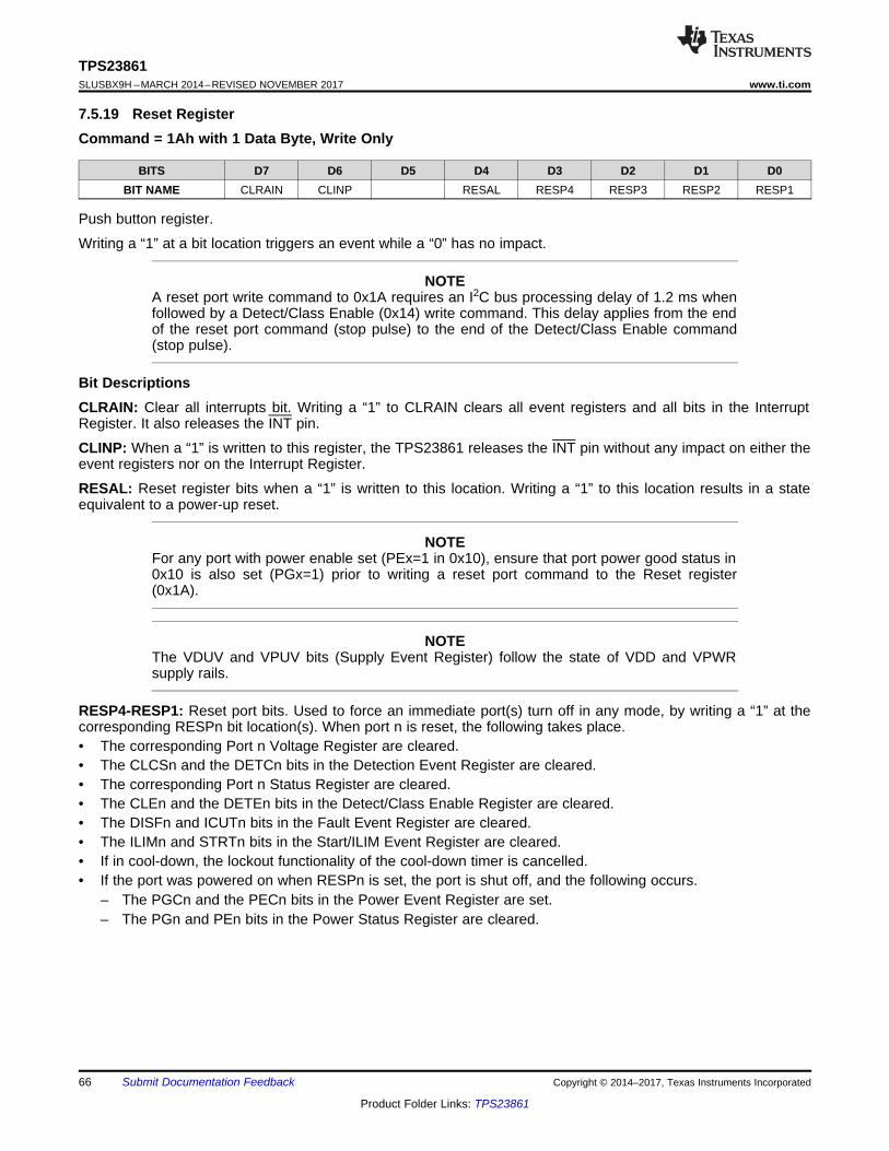
66
TPS23861SLUSBX9H –MARCH 2014–REVISED NOVEMBER 2017 www.ti.com
Product Folder Links: TPS23861
Submit Documentation Feedback Copyright © 2014–2017, Texas Instruments Incorporated
7.5.19 Reset RegisterCommand = 1Ah with 1 Data Byte, Write Only
BITS D7 D6 D5 D4 D3 D2 D1 D0BIT NAME CLRAIN CLINP RESAL RESP4 RESP3 RESP2 RESP1
Push button register.
Writing a “1” at a bit location triggers an event while a “0” has no impact.
NOTEA reset port write command to 0x1A requires an I2C bus processing delay of 1.2 ms whenfollowed by a Detect/Class Enable (0x14) write command. This delay applies from the endof the reset port command (stop pulse) to the end of the Detect/Class Enable command(stop pulse).
Bit DescriptionsCLRAIN: Clear all interrupts bit. Writing a “1” to CLRAIN clears all event registers and all bits in the InterruptRegister. It also releases the INT pin.
CLINP: When a “1” is written to this register, the TPS23861 releases the INT pin without any impact on either theevent registers nor on the Interrupt Register.
RESAL: Reset register bits when a “1” is written to this location. Writing a “1” to this location results in a stateequivalent to a power-up reset.
NOTEFor any port with power enable set (PEx=1 in 0x10), ensure that port power good status in0x10 is also set (PGx=1) prior to writing a reset port command to the Reset register(0x1A).
NOTEThe VDUV and VPUV bits (Supply Event Register) follow the state of VDD and VPWRsupply rails.
RESP4-RESP1: Reset port bits. Used to force an immediate port(s) turn off in any mode, by writing a “1” at thecorresponding RESPn bit location(s). When port n is reset, the following takes place.• The corresponding Port n Voltage Register are cleared.• The CLCSn and the DETCn bits in the Detection Event Register are cleared.• The corresponding Port n Status Register are cleared.• The CLEn and the DETEn bits in the Detect/Class Enable Register are cleared.• The DISFn and ICUTn bits in the Fault Event Register are cleared.• The ILIMn and STRTn bits in the Start/ILIM Event Register are cleared.• If in cool-down, the lockout functionality of the cool-down timer is cancelled.• If the port was powered on when RESPn is set, the port is shut off, and the following occurs.
– The PGCn and the PECn bits in the Power Event Register are set.– The PGn and PEn bits in the Power Status Register are cleared.

67
TPS23861www.ti.com SLUSBX9H –MARCH 2014–REVISED NOVEMBER 2017
Product Folder Links: TPS23861
Submit Documentation FeedbackCopyright © 2014–2017, Texas Instruments Incorporated
7.5.20 Legacy Detect Mode RegisterCommand = 20h with 1 Data Byte, Read/Write
BITS D7 D6 D5 D4 D3 D2 D1 D0BIT NAME LEGMOD4 LEGMOD3 LEGMOD2 LEGMOD1
RESET or POR VALUE 00 00 00 00
Legacy-detect operation is described in Legacy Device Detection. The TPS23861 can perform a legacy-detectoperation only or a standard detection followed by a legacy-detect operation when directed by the RDETn push-button command in the Detect/Class Restart Register, or in Semi-Auto or Auto Mode when the DETEn bit in theDetect/Class Enable Register is set. Note that in Semi-Auto or in Auto Mode, the port will not automaticallypower up if a legacy device is detected. In these cases, the port must be powered on by the host.
Bit DescriptionsLEGMODn[1:0]: Legacy-detection-mode field. This field defines the Legacy-Detect Mode of Port n as follows.
LEGMODn[1:0] LEGACY DETECT MODE00 Legacy detect disabled; if DETEn bit in Detect/Class Enable Register is set, a standard
(resistance only) detection sequence will be performed.01 Legacy detect sequence only; if DETEn bit in Detect/Class Enable Register is set, a legacy
detect sequence will be performed10 Standard + legacy detect sequence; if DETEn bit in Detect/Class Enable Register is set, a
standard detection followed by legacy detect sequence will be performed11 Reserved
7.5.21 Two-Event Classification RegisterCommand = 21h with 1 Data Byte, Read/Write
BITS D7 D6 D5 D4 D3 D2 D1 D0BIT NAME TECLEN4 TECLEN3 TECLEN2 TECLEN1
RESET or POR VALUE 0A 0A 0A 0A
The Two-Event Classification Register controls whether a second physical-layer classification event occurs aftera class 4 PD is classified under the following circumstances:• In Manual Mode, when CLEn is set or a pushbutton RCLn bit is written.• In Semi-Auto Mode, when CLEn is set or a PWONn pushbutton command is written.• In Auto Mode
Bit DescriptionsTECLENn[1:0]: The TECLENn field sets the conditions for PSE-initiated two-event physical layer classificationas follows. The details of these conditions depend on the operating mode as outlined in the preceding paragraphand the Device Functional Modes section.
Table 11. TECLENn Field EncodingTECLENn[1:0] CONDITIONS FOR TWO-EVENT PHYSICAL-LAYER CLASSIFICATION
00 Two-event physical-layer classification is disabled01 A second classification event is initiated if a class 4 classification event occurs10 Reserved11 A second classification event is initiated if a class 4 classification event occurs

STEPt N t u
68
TPS23861SLUSBX9H –MARCH 2014–REVISED NOVEMBER 2017 www.ti.com
Product Folder Links: TPS23861
Submit Documentation Feedback Copyright © 2014–2017, Texas Instruments Incorporated
7.5.22 Interrupt Timer RegisterCommand = 27h with 1 Data Byte, Read/Write
BITS D7 D6 D5 D4 D3 D2 D1 D0BIT NAME R27[7] R27[6] R27[5] R27[4] TMR[3] TMR[2] TMR[1] TMR[0]RESET OR
POR VALUE0 0 0 0 0 0 0 0
Bit DescriptionsTMR[3:0]: Non-critical interrupts may be deferred using an internal timer. Once loaded with a non-zero value, theinternal timer counts continuously with period calculated as follows:
where• t = Timer period, ms• N = 4-bit value in TMR[3:0] field• tSTEP = 10 ms (1)
Non-critical interrupts generated within the TPS23861 will be passed to the interrupt-handling hardwarewhenever the timer counts down to 0. (The timer then reloads and continues to count.)
NOTE‘interrupt-handling hardware’ includes all interrupt-enabling functionality as well.
Critical and non-critical interrupts are defined in Table 6. When the TMR[3:0] field is read, the contents will be thecontents last written by firmware.
When TMR[3:0] = 0 all interrupts will be handled as they are generated. In other words, this function is disabledwhen TMR[3:0] = 0000.
Reserved: Bits R27[7:4] are reserved for future use. Undesirable behavior may result if the value of these bitsare changed from the reset value.

69
TPS23861www.ti.com SLUSBX9H –MARCH 2014–REVISED NOVEMBER 2017
Product Folder Links: TPS23861
Submit Documentation FeedbackCopyright © 2014–2017, Texas Instruments Incorporated
7.5.23 Disconnect Threshold RegisterCommand = 29h with 1 Data Byte, Read/Write
BITS D7 D6 D5 D4 D3 D2 D1 D0BIT NAME DCTH4 DCTH3 DCTH2 DCTH1
RESET or POR VALUE 00 00 00 00
Disconnect current thresholds may be programmed individually for each port.
7.5.23.1 Bits DescriptionDCTHn[1:0]: A 2-bit field used to set the current threshold for disconnect. If the port is powered on and thecurrent goes below the disconnect threshold set by DCTHn, the TDIS counter is started. If the TDIS timer timesout the port is powered down.
DCTHn FIELD DISCONNECT THRESHOLD, mA00 7.501 1510 3011 50

70
TPS23861SLUSBX9H –MARCH 2014–REVISED NOVEMBER 2017 www.ti.com
Product Folder Links: TPS23861
Submit Documentation Feedback Copyright © 2014–2017, Texas Instruments Incorporated
7.5.24 ICUTnm CONFIG Register
7.5.24.1 ICUT21 CONFIG RegisterCommand = 2Ah with 1 Data Byte, Read/Write
BITS D7 D6 D5 D4 D3 D2 D1 D0BIT NAME ICUT Port 2 ICUT Port 1
RESET or POR VALUE 0 0 0 0 0 0 0 0
7.5.24.2 ICUT43 CONFIG RegisterCommand = 2Bh with 1 Data Byte, Read/Write
BITS D7 D6 D5 D4 D3 D2 D1 D0BIT NAME ICUT Port 4 ICUT Port 3
RESET or POR VALUE 0 0 0 0 0 0 0 0
(1) PoEPn bit should be set according to ICUT value for host to ensure the ICUT and ILIM relationship.
7.5.24.3 Bits DescriptionICUT Port n[2:0]: is a 3-bit field used to set the ICUT current threshold. If the current threshold set by ICUT Portn is exceeded, the TICUT timer begins to count. When the terminal count (0) is reached, an ICUT fault isdeclared, and the port is shut down.
NOTEThe current values in the following table are nominal values.
ICUT PORT n FIELD ICUT (mA) PoEPn (1)
000 374 0001 110 0010 204 0011 374 0100 754 1101 592 1110 645 1111 920 1

STEPT 20 N T u
71
TPS23861www.ti.com SLUSBX9H –MARCH 2014–REVISED NOVEMBER 2017
Product Folder Links: TPS23861
Submit Documentation FeedbackCopyright © 2014–2017, Texas Instruments Incorporated
7.5.25 Temperature RegisterCommand = 2Ch with 1 Data Byte, Read Only
BITS D7 D6 D5 D4 D3 D2 D1 D0BIT NAME Temp[7:0]
RESET or POR VALUE 0 0 0 0 0 0 0 0
Die temperature register.
Bit DescriptionsTemp[7:0]: 8-bit data conversion result of temperature. The equation defining the temperature measured is:
where• T = temperature, °C• TSTEP = LSB value• N = 8-bit value in Temp[7:0] (2)
MODE FULL SCALE VALUE LSB VALUEAny 150°C (typical) 0.7°C
NOTETemperature sensor performance is only typical, not production tested and not ensured.

STEPV N V u
72
TPS23861SLUSBX9H –MARCH 2014–REVISED NOVEMBER 2017 www.ti.com
Product Folder Links: TPS23861
Submit Documentation Feedback Copyright © 2014–2017, Texas Instruments Incorporated
7.5.26 Input Voltage RegisterCommand = 2Eh with 2 Data Byte (LSByte first, MSByte second), Read OnlyLSB: 2Eh
BITS D7 D6 D5 D4 D3 D2 D1 D0BIT NAME Input Voltage[7:0]
RESET or POR VALUE 0 0 0 0 0 0 0 0
MSB: 2Fh
BITS D7 D6 D5 D4 D3 D2 D1 D0BIT NAME Input Voltage[13:8]
RESET or POR VALUE 0 0 0 0 0 0 0 0
Bit DescriptionsData conversion result. The I2C data transmission is a 2-byte transfer.
Input Voltage[13:0]: 14-bit Data conversion result of input voltage. The update rate is approximately 1 persecond.
The equation defining the voltage measured is:
where• V = input voltage, V• N = 14 bit value in input voltage register• VSTEP = LSB value (3)
MODE FULL SCALE VALUE LSB VALUEAny 60 V 3.662 mV
NOTEThe measurement is made between VPWR and AGND.

73
TPS23861www.ti.com SLUSBX9H –MARCH 2014–REVISED NOVEMBER 2017
Product Folder Links: TPS23861
Submit Documentation FeedbackCopyright © 2014–2017, Texas Instruments Incorporated
7.5.27 Port n Current Register
7.5.27.1 Port 1 Current RegisterCommand = 30h with 2 Data Byte (LSByte first, MSByte second), Read OnlyLSB: 30h
BITS D7 D6 D5 D4 D3 D2 D1 D0BIT NAME Port 1 Current[7:0]
RESET or POR VALUE 0 0 0 0 0 0 0 0
MSB: 31h
BITS D7 D6 D5 D4 D3 D2 D1 D0BIT NAME Port 1 Current[13:8]
RESET or POR VALUE 0 0 0 0 0 0 0 0
7.5.27.2 Port 2 Current RegisterCommand = 34h with 2 Data Byte (LSByte first, MSByte second), Read OnlyLSB: 34h
BITS D7 D6 D5 D4 D3 D2 D1 D0BIT NAME Port 2 Current[7:0]
RESET or POR VALUE 0 0 0 0 0 0 0 0
MSB: 35h
BITS D7 D6 D5 D4 D3 D2 D1 D0BIT NAME - - Port 2 Current[13:8]
RESET or POR VALUE 0 0 0 0 0 0 0 0
7.5.27.3 Port 3 Current RegisterCommand = 38h with 2 Data Byte (LSByte first, MSByte second), Read OnlyLSB: 38h
BITS D7 D6 D5 D4 D3 D2 D1 D0BIT NAME Port 3 Current[7:0]
RESET or POR VALUE 0 0 0 0 0 0 0 0
MSB: 39h
BITS D7 D6 D5 D4 D3 D2 D1 D0BIT NAME Port 3 Current[13:8]
RESET or POR VALUE 0 0 0 0 0 0 0 0

STEPI N I u
74
TPS23861SLUSBX9H –MARCH 2014–REVISED NOVEMBER 2017 www.ti.com
Product Folder Links: TPS23861
Submit Documentation Feedback Copyright © 2014–2017, Texas Instruments Incorporated
7.5.27.4 Port 4 Current RegisterCommand = 3Ch with 2 Data Byte (LSByte first, MSByte second), Read OnlyLSB: 3Ch
BITS D7 D6 D5 D4 D3 D2 D1 D0BIT NAME Port 4 Current[7:0]
RESET or POR VALUE 0 0 0 0 0 0 0 0
MSB: 3Dh
BITS D7 D6 D5 D4 D3 D2 D1 D0BIT NAME Port 4 Current[13:8]
RESET or POR VALUE 0 0 0 0 0 0 0 0
Port current is monitored continuously when:• The port is powered on.• The port is in Off Mode. Data conversion result.
The I2C data transmission is a 2-byte transfer.
NOTEThe conversion is done using a TI-proprietary multi-slope integrating converter.
Bit DescriptionsPort n Current[13:0]: 14-bit data conversion result of current for Port n. The result depends on whether thecurrent-sense resistor is 250 mΩ or 255 mΩ.
The equation defining the current measured is:
where• I = Port n Current, A• N = 14-bit value in Port n Current Register• ISTEP = LSB value (4)
RS = 255 mΩ RSENSE = 250 mΩFULL SCALE LSB VALUE FULL SCALE LSB VALUE
1 A 61.039 µA 1.02 A 62.260 µA

75
TPS23861www.ti.com SLUSBX9H –MARCH 2014–REVISED NOVEMBER 2017
Product Folder Links: TPS23861
Submit Documentation FeedbackCopyright © 2014–2017, Texas Instruments Incorporated
7.5.28 Port n Voltage Register
7.5.28.1 Port 1 Voltage RegisterCommand = 32h with 2 Data Byte (LSByte first, MSByte second), Read OnlyLSB: 32h
BITS D7 D6 D5 D4 D3 D2 D1 D0BIT NAME Port 1 Voltage[7:0]
RESET or POR VALUE 0 0 0 0 0 0 0 0
MSB: 33h
BITS D7 D6 D5 D4 D3 D2 D1 D0BIT NAME Port 1 Voltage[13:8]
RESET or POR VALUE 0 0 0 0 0 0 0 0
7.5.28.2 Port 2 Voltage RegisterCommand = 36h with 2 Data Byte (LSByte first, MSByte second), Read OnlyLSB: 36h
BITS D7 D6 D5 D4 D3 D2 D1 D0BIT NAME Port 2 Voltage[7:0]
RESET or POR VALUE 0 0 0 0 0 0 0 0
MSB: 37h
BITS D7 D6 D5 D4 D3 D2 D1 D0BIT NAME Port 2 Voltage[13:8]
RESET or POR VALUE 0 0 0 0 0 0 0 0
7.5.28.3 Port 3 Voltage RegisterCommand = 3Ah with 2 Data Byte (LSByte first, MSByte second), Read OnlyLSB: 3Ah
BITS D7 D6 D5 D4 D3 D2 D1 D0BIT NAME Port 3 Voltage[7:0]
RESET or POR VALUE 0 0 0 0 0 0 0 0
MSB: 3Bh
BITS D7 D6 D5 D4 D3 D2 D1 D0BIT NAME Port 3 Voltage[13:8]
RESET or POR VALUE 0 0 0 0 0 0 0 0

STEPV N V u
76
TPS23861SLUSBX9H –MARCH 2014–REVISED NOVEMBER 2017 www.ti.com
Product Folder Links: TPS23861
Submit Documentation Feedback Copyright © 2014–2017, Texas Instruments Incorporated
7.5.28.4 Port 4 Voltage RegisterCommand = 3Eh with 2 Data Byte (LSByte first, MSByte second), Read OnlyLSB: 3Eh
BITS D7 D6 D5 D4 D3 D2 D1 D0BIT NAME Port 4 Voltage[7:0]
RESET or POR VALUE 0 0 0 0 0 0 0 0
MSB: 3Fh
BITS D7 D6 D5 D4 D3 D2 D1 D0BIT NAME Port 4 Voltage[13:8]
RESET or POR VALUE 0 0 0 0 0 0 0 0
Port voltage is monitored continuously when• The port is powered on.• The port is in Off Mode.
Data conversion result. The I2C data transmission is a 2-byte transfer.
Bit DescriptionsPort n Voltage[13:0]: 14-bit Data conversion result of voltage for port n. The equation defining the voltagemeasured is:
where• V = Port n Voltage, V• N = 14-bit value in Port n Voltage Register• VSTEP = LSB Value (5)
FULL SCALE VALUE LSB VALUE60 V 3.662 mV
NOTEThe port voltage measurement is made between VPWR and DRAINn.

77
TPS23861www.ti.com SLUSBX9H –MARCH 2014–REVISED NOVEMBER 2017
Product Folder Links: TPS23861
Submit Documentation FeedbackCopyright © 2014–2017, Texas Instruments Incorporated
7.5.29 PoE Plus RegisterCommand = 40h with 1 Data Byte, R/W
BITS D7 D6 D5 D4 D3 D2 D1 D0BIT NAME PoEP4 PoEP3 PoEP2 PoEP1
RESET or POR VALUE 0 0 0 0
The POEPn bit can be set or cleared by the host processor over the I2C interface. Additionally, the bit is setwhen in Auto Mode before the port is powered on following the recognition of a valid Class 4 PD. Likewise, thePOEPn bit is cleared before the port is powered on when in Auto Mode and a Class 0, 1, 2 or 3 PD isrecognized.
One POEPn bit supports each port. When the POEPn bit for a port is set:• 2 x ILIM foldback curve is applied to a port when the port is powered on. See Figure 58.• The short-circuit protection threshold (ILIM) for the FET is increased by a factor of 2.5 with respect to the
POEPn-bit-cleared value.• The tLIM value is selectable via the TLIM timer field in the Timing Configuration Register.
Likewise, when the POEPn bit for a port is cleared:• 1 x ILIM foldback curve is applied to a port when the port is powered on. See Figure 58.• The short-circuit protection threshold (ILIM) for the FET is reduced to a value of 40% of the POEPn-bit-set
value.• The tLIM value is set to 60 ms.
The inrush-foldback behavior is not affected by the setting of the POEPn bit. See Figure 57.
Bit DescriptionsPoEPn: PoE+ bits. Setting this bit causes the 2 x ILIM foldback curve to be applied to Port n.
1 = Use 2 x ILIM foldback curve on Port n.
0 = Use 1 x ILIM foldback curve on Port n.
NOTEPoEPn bit should be set according to ICUT value for host to ensure the ICUT and ILIMrelationship. See Table 15
7.5.30 Firmware Revision RegisterCommand = 41h with 1 Data Byte, Read Only
BITS D7 D6 D5 D4 D3 D2 D1 D0BIT NAME FRV
RESET or POR VALUE R R R R R RRR
Bit DescriptionsFRV[2:0]: Firmware revision number.

78
TPS23861SLUSBX9H –MARCH 2014–REVISED NOVEMBER 2017 www.ti.com
Product Folder Links: TPS23861
Submit Documentation Feedback Copyright © 2014–2017, Texas Instruments Incorporated
7.5.31 I2C Watchdog RegisterCommand = 42h with 1 Data Byte, R/W
BITS D7 D6 D5 D4 D3 D2 D1 D0BIT NAME IWD[3:0] WDS
RESET or POR VALUE 1 0 1 1 0
The I2C watchdog timer monitors the I2C clock line in order to prevent hung software situations that could leaveports in a hazardous state. The timer can be reset by either edge on SCL input. If the watchdog timer times out,the WDS bit is set. Depending on the value of IWD, all ports may be powered down. The nominal watchdog time-out period is 2 seconds.
When the ports are powered down due to a watchdog event, the corresponding bits are cleared in the DetectionEvent Register (CLSCn, DETn), Fault Event register (DISFn, ICUTn), Start/ILIM Event Register (STRTn), Port nStatus Registers (Class Pn, Detect Pn) and Detect/Class Enable Register (CLEn, DETEn).
The corresponding PEn and PGn bits of the Power Status Register are also updated accordingly.
Bit DescriptionsIWD3 - IWD0: I2C Watchdog disable. When equal to 1011, the watchdog is masked. Otherwise, it is umaskedand the watchdog is operational.
WDS: I2C Watchdog timer status, valid even if the watchdog is masked. When set, it means that the watchdogtimer has expired without any activity on I2C clock line. Writing 0 at WDS location clears it.
NOTEwhen the watchdog timer expires and if the watchdog is unmasked, all ports are alsoturned off.
When the ports are turned OFF due to I2C watchdog, the corresponding bits in Detection Event Register(CLSCn, DETCn), Fault Event Register (DISFn, ICUTn), Start Event Register (STRTn), Port n Status register(Class Pn, Detect Pn), Detect/Class Enable Register (CLEn, DETEn) and Power-On Fault Register (PFn) arealso cleared. The corresponding PGCn and PECn bits of Power Event register is set if there is a change. Thecorresponding PEn and PGn bits of Power Status Register are updated accordingly.
7.5.32 Device ID RegisterCommand = 43h with 1 Data Byte, R/W
BITS D7 D6 D5 D4 D3 D2 D1 D0BIT NAME DID SR
RESET or POR VALUE 1 1 1 SR[4:0]
Bit DescriptionsDID: Device ID number (111).
SR: Silicon Revision number.

79
TPS23861www.ti.com SLUSBX9H –MARCH 2014–REVISED NOVEMBER 2017
Product Folder Links: TPS23861
Submit Documentation FeedbackCopyright © 2014–2017, Texas Instruments Incorporated
7.5.33 Cool Down/Gate Drive RegisterCommand = 45h with 1 Data Byte, R/W
BITS D7 D6 D5 D4 D3 D2 D1 D0BIT NAME CLDN IGATE
RESET or POR VALUE 0 0 0 0 0 0 0 0
These bits are applicable to all four ports.
Bit DescriptionsCLDN: Fault Cool-Down Timer Programming Field. Following a Start, ICUT or ILIM, a port shuts down, and thecool-down timer counts down. Until the timer counts down to 0, the port will not be allowed to be powered on ifthe port is in Semi-Auto or Auto Mode. If in Manual Mode, the port can be powered on immediately with a push-button command by writing to PWONn in the Power Enable Register. The cool-down timer is cancelled by power-on reset, device reset or port reset (see Reset Register).
The field programming is:
CLDN[1:0] NOMINAL COOL-DOWN TIMER PERIOD0X 1 s10 2 s11 4 s
IGATE: GATE Pull-Up Current Bit. IGATE sets the gate pull-up current.
IGATE NOMINAL GATE PULLUP CURRENT (µA)0 501 25

80
TPS23861SLUSBX9H –MARCH 2014–REVISED NOVEMBER 2017 www.ti.com
Product Folder Links: TPS23861
Submit Documentation Feedback Copyright © 2014–2017, Texas Instruments Incorporated
7.5.34 Port n Detect Resistance Register
7.5.34.1 Port 1 Detect Resistance RegisterCommand = 60h with 2 Data Byte (LSByte first, MSByte second), Read OnlyLSB: 60h
BITS D7 D6 D5 D4 D3 D2 D1 D0BIT NAME Port 1 Resistance[7:0]
RESET or POR VALUE 0 0 0 0 0 0 0 0
MSB: 61h
BITS D7 D6 D5 D4 D3 D2 D1 D0BIT NAME RS1[1:0] Port 1 Resistance[13:8]
RESET or POR VALUE 0 0 0 0 0 0 0 0
7.5.34.1.1 Port 2 Detect Resistance Register
Command = 62h with 2 Data Byte (LSByte first, MSByte second), Read OnlyLSB: 62h
BITS D7 D6 D5 D4 D3 D2 D1 D0BIT NAME Port 2 Resistance[7:0]
RESET or POR VALUE 0 0 0 0 0 0 0 0
MSB: 63h
BITS D7 D6 D5 D4 D3 D2 D1 D0BIT NAME RS2[1:0] Port 2 Resistance[13:8]
RESET or POR VALUE 0 0 0 0 0 0 0 0
7.5.34.1.2 Port 3 Detect Resistance Register
Command = 64h with 2 Data Byte (LSByte first, MSByte second), Read OnlyLSB: 64h
BITS D7 D6 D5 D4 D3 D2 D1 D0BIT NAME Port 3 Resistance[7:0]
RESET or POR VALUE 0 0 0 0 0 0 0 0
MSB: 65h
BITS D7 D6 D5 D4 D3 D2 D1 D0BIT NAME RS3[1:0] Port 3 Resistance[13:8]
RESET or POR VALUE 0 0 0 0 0 0 0 0

STEPR N R u
81
TPS23861www.ti.com SLUSBX9H –MARCH 2014–REVISED NOVEMBER 2017
Product Folder Links: TPS23861
Submit Documentation FeedbackCopyright © 2014–2017, Texas Instruments Incorporated
7.5.34.1.3 Port 4 Detect Resistance Register
Command = 66h with 2 Data Byte (LSByte first, MSByte second), Read OnlyLSB: 66h
BITS D7 D6 D5 D4 D3 D2 D1 D0BIT NAME Port 4 Resistance[7:0]
RESET or POR VALUE 0 0 0 0 0 0 0 0
MSB: 67h
BITS D7 D6 D5 D4 D3 D2 D1 D0BIT NAME RS4[1:0] Port 4 Resistance[13:8]
RESET or POR VALUE 0 0 0 0 0 0 0 0
Bit DescriptionsMost recent 2 point detection resistance measurement. The resistance value shown is usable only if RSn[1:0] areat 00 or 01. The I2C data transmission is a 2 byte transfer.
Port n Resistance[13:0]: 14-bit data conversion result of detection resistance for port n. The equation definingthe resistance measured is:
where• R = Detection resistance, Ω• N = 14-bit value in Port n Resistance Register• RSTEP = LSB value (6)
USEABLE RESISTANCE RANGE LSB VALUE500 Ω to 55 kΩ 11.0966 Ω
RSn[1:0]: Most recent detection result status on port n. If the state is 00, the 14-bit resistance value is calculatedwith a bit weight of 11.0966 Ω/bit. If the state is 01, two additional detection fingers have been performed athigher detection currents (270 µA and 540 µA) in order to better measure the lower port impedance. The 14-bitresistance value is calculated with a bit weight of 4.625 Ω/bit in this case. The detection result is maintained inthe register in any operating mode following the detection.
RSn1 RSn0 DETECT STATUS RSTEP BIT WEIGHT0 0 Other 11.0966 Ω/bit0 1 Low (< 2 kΩ) Additional detect 4.625 Ω/bit1 0 Open circuit N/A1 1 MOSFET short fault N/A

82
TPS23861SLUSBX9H –MARCH 2014–REVISED NOVEMBER 2017 www.ti.com
Product Folder Links: TPS23861
Submit Documentation Feedback Copyright © 2014–2017, Texas Instruments Incorporated
7.5.35 Port n Detect Voltage Difference Register
7.5.35.1 Port 1 Detect Voltage Difference RegisterCommand = 68h with 2 Data Byte (LSByte first, MSByte second), Read OnlyLSB: 68h
BITS D7 D6 D5 D4 D3 D2 D1 D0BIT NAME Port 1 Voltage Difference [7:0]
RESET or POR VALUE 0 0 0 0 0 0 0 0
MSB: 69h
BITS D7 D6 D5 D4 D3 D2 D1 D0BIT NAME VDS1[3:0] Port 1 Voltage Difference [11:8]
RESET or POR VALUE 0 0 0 0 0 0 0 0
7.5.35.2 Port 2 Detect Voltage Difference RegisterCommand = 6Ah with 2 Data Byte (LSByte first, MSByte second), Read OnlyLSB: 6Ah
BITS D7 D6 D5 D4 D3 D2 D1 D0BIT NAME Port 2 Voltage Difference [7:0]
RESET or POR VALUE 0 0 0 0 0 0 0 0
MSB: 6Bh
BITS D7 D6 D5 D4 D3 D2 D1 D0BIT NAME VDS2[3:0] Port 2 Voltage Difference [11:8]
RESET or POR VALUE 0 0 0 0 0 0 0 0
7.5.35.3 Port 3 Detect Voltage Difference RegisterCommand = 6Ch with 2 Data Byte (LSByte first, MSByte second), Read OnlyLSB: 6Ch
BITS D7 D6 D5 D4 D3 D2 D1 D0BIT NAME Port 3 Voltage Difference [7:0]
RESET or POR VALUE 0 0 0 0 0 0 0 0
MSB: 6Dh
BITS D7 D6 D5 D4 D3 D2 D1 D0BIT NAME VDS3[3:0] Port 3 Voltage Difference [11:8]
RESET or POR VALUE 0 0 0 0 0 0 0 0

STEP
kC
N V#
u
83
TPS23861www.ti.com SLUSBX9H –MARCH 2014–REVISED NOVEMBER 2017
Product Folder Links: TPS23861
Submit Documentation FeedbackCopyright © 2014–2017, Texas Instruments Incorporated
7.5.35.4 Port 4 Detect Voltage Difference RegisterCommand = 6Eh with 2 Data Byte (LSByte first, MSByte second), ReadLSB: 6Eh
BITS D7 D6 D5 D4 D3 D2 D1 D0BIT NAME Port 4 Voltage Difference [7:0]
RESET or POR VALUE 0 0 0 0 0 0 0 0
MSB: 6Fh
BITS D7 D6 D5 D4 D3 D2 D1 D0BIT NAME VDS4[3:0] Port 4 Voltage Difference [11:8]
RESET or POR VALUE 0 0 0 0 0 0 0 0
This register is used to determine the presence of a legacy PD by measuring the PD input capacitance on the PI.A charge is injected into the PI, and the resulting Δv is reported. The Δv value shown is useable only if VDSn[3:0]= 0001.
The I2C data transmission is a 2-byte transfer.
Bit DescriptionsPort n Voltage Difference[11:0]: 12-bit data conversion result of the difference in voltage on the port as a resultof a fixed charge injected into the port. The equation defining the resistance measured is:
where• C = Port capacitance, F• k = 81 x 10-6 coulomb• N = 12-bit value in Port n Detect Voltage Difference Register• VSTEP = LSB Value (7)
NOTEThe expression for port capacitance ignores the effect of any conductance in parallel withthe capacitance being measured. The effect of parallel conductance is to give a highervalue than the actual value of any capacitance present.
USEABLE CAPACITANCE RANGE VOLTAGE DIFFERENCE LSB VALUE10 to 100 µF 4.884 mV

84
TPS23861SLUSBX9H –MARCH 2014–REVISED NOVEMBER 2017 www.ti.com
Product Folder Links: TPS23861
Submit Documentation Feedback Copyright © 2014–2017, Texas Instruments Incorporated
VDSn[3:0]: Most recent detect voltage difference result status on Port n. If “0001” state, the 12-bit Δv value isuseable.
This measurement is made on a port if legacy detect is enabled using the Legacy Detect Mode Register.
VDSn is set to the Power-On Reset State (0000b) when legacy detection is enabled until a Δv measurement ismade.
The detection result is maintained in the register in any operating mode following the measurement.
The selection is as following:
VDSn[3:0] VOLTAGE-DIFFERENCE MEASUREMENT STATUS0000 Power-on reset0001 Valid measurement0010 Unable to discharge PD input capacitance to 2.4 V before timeout0011 Unable to achieve 0.4V to take first measurement before timeout0100 First measurement exceeds VDet-clamp (min)0101 Second measurement exceeds VDet-clamp (min)0110 ΔV < 0.5 V (insufficient signal)
7.5.36 Reserved Registers• Register 0x1B• Register 0x1D• Register 0x1E• Register 0x1F• Register 0x22• Register 0x23• Register 0x24• Register 0x25• Register 0x59
Reserved: These registers are reserved for manufacturing or future use. Undesirable behavior may result ifthese registers are written to.

14
13
12
11
10
9
8
7
6
5
4
3
2
1 VDD
SCL
SDAI
SDAO
DGND
SEN3
DRAIN3
GATE3
KSENSB
SEN4
DRAIN4
GATE4 15
16
17
18
19
20
21
22
23
24
25
26
27
28VPWR
N/C
AOUT
AIN
SHTDWN
A3
AGND
GATE2
DRAIN2
SEN2
KSENSA
GATE1
DRAIN1
SEN1
RESET
INT
22.1:
:
0.1PF50V
0.1PF100V
: :
:
22.1:
22.1:
22.1:
SMBJ58A-13-F 0.1PF100V
FDMC3612
:
10MQ100NTRPBF
C1S 1.5
VPWRP2
+
-
RJ45
&
XFMR
SMBJ58A-13-F0.1PF100V
FDMC3612
:
10MQ100NTRPBF
C1S 1.5
VPWR
P1
+
-RJ45
&
XFMR
(Optional)
(Optional)
TPS23861PW
SMBJ58A-13-F0.1PF100V
FDMC3612
:
10MQ100NTRPBF
C1S 1.5
VPWRP3
+
-
RJ45
&
XFMR
SMBJ58A-13-F
0.1PF100V
FDMC3612
:
10MQ100NTRPBF
C1S 1.5
VPWR
P4
+
-RJ45
&
XFMR
(Optional)
(Optional)
VPWRVDD
Copyright © 2016, Texas Instruments Incorporated
85
TPS23861www.ti.com SLUSBX9H –MARCH 2014–REVISED NOVEMBER 2017
Product Folder Links: TPS23861
Submit Documentation FeedbackCopyright © 2014–2017, Texas Instruments Incorporated
8 Application and Implementation
NOTEInformation in the following applications sections is not part of the TI componentspecification, and TI does not warrant its accuracy or completeness. TI’s customers areresponsible for determining suitability of components for their purposes. Customers shouldvalidate and test their design implementation to confirm system functionality.
8.1 Introduction to PoEPower-over-Ethernet (PoE) is a means of distributing power to Ethernet devices over the Ethernet cable usingeither data or spare pairs. PoE eliminates the need for power supplies at the Ethernet device. Commonapplications of PoE are security cameras, IP Phones and PDA chargers. The host or mid-span equipment thatsupplies power is the Power Source Equipment (PSE). The load at the Ethernet connector is the Powered device(PD). PoE protocol between PSE and PD controlling power to the load is specified by IEEE Std 802.3at-2009.Transformers are used at Ethernet host ports, mid-spans and hubs, to interface data to the cable. A DC voltagecan be applied to the center tap of the transformer with no effect on the data signals. As in any powertransmission line, a relatively high 48 V is used to keep current low, minimize the effect of IR drops in the lineand preserve power to the load. Standard POE delivers approximately 13 W to a type 1 PD, and 25.5 W to atype 2 PD. Figure 46 shows the overview schematic of a POE port.
8.2 Application InformationThe TPS23861 is a four port, IEEE 802.3at PoE PSE controller and can be used in very simple, low port count,automatic or high port count micro-controller managed applications.
Subsequent sections describe detailed design procedures for applications with different requirements includinghost control.
Figure 46. Automatic 4-Port Operation Schematic

KSENSB
SEN4
DRAIN4
GATE4
KSENSA
GATE1
DRAIN1
SEN1 15
16
17
18
14
13
12
11
22 :255 m 250 m
47 :
Port 4 Not Used
86
TPS23861SLUSBX9H –MARCH 2014–REVISED NOVEMBER 2017 www.ti.com
Product Folder Links: TPS23861
Submit Documentation Feedback Copyright © 2014–2017, Texas Instruments Incorporated
Application Information (continued)The schematic of Figure 46 depicts automatic mode operation of the TPS23861, providing turnkey functionalityready to power PoE loads. No connection to the I2C bus or any type of host control is required. In Figure 46 theTPS23861 automatically:1. Performs load detection.2. Performs classification including type-2 (two-finger) of up to Class 4 loads.3. Enables power with protective foldback current limiting, and ICUT value based on load class.4. Shuts down in the event of fault loads and shorts.5. Performs Maintain Power Signature function to ensure removal of power if load is disconnected.6. Undervoltage lock out occurs if VPWR falls below VPUV_F (typical 26.5 V).
Following a power-off command, disconnect or shutdown due to a start, ICUT or ILIM fault, the port powersdown. Following port power off due to a power off command or disconnect, the TPS23861 continues automaticoperation starting with a detection cycle. If the shutdown is due to a start, ICUT or ILIM fault, the TPS23861enters into a cool-down period. After the end of the cool-down period the TPS23861 continues automaticoperation starting with a detection cycle.
The TPS23861 will not automatically apply power to a port under the following circumstances:• The detect status is not Resistance Valid.• If the classification status is overcurrent, class mismatch, or unknown.
8.2.1 Kelvin Current Sensing ResistorLoad current in each PSE port is sensed as the voltage across a low-end current-sense resistor with a value of255 mΩ. For more accurate current sensing, kelvin sensing of the low end of the current-sense resistor isprovided through pins KSENSA for ports 1 and 2, and KSENSB for ports 3 and 4.
8.2.2 Connections on Unused PortsThe TPS23861 can be used on applications needing only 1 to 4 ports. On unused ports ground the SENx pinand leave the GATEx pin floating. DRAINx pins can be grounded or left open (leaving open may slightly reducepower consumption). One example of an unused PORT4 is shown in Figure 47. For detailed design andcomponent selection information, see System Examples.
This schematic shows connections for an unused PORT4.
Figure 47. Unused PORT4 Connections

14
13
12
11
10
9
8
7
6
5
4
3
2
1 VDD
SCL
SDAI
SDAO
DGND
SEN3
DRAIN3
GATE3
KSENSB
SEN4
DRAIN4
GATE4 15
16
17
18
19
20
21
22
23
24
25
26
27
28VPWR
N/C
AOUT
AIN
SHTDWN
A3
AGND
GATE2
DRAIN2
SEN2
KSENSA
GATE1
DRAIN1
SEN1
RESET
INT
RSEN2
CVDD CVPWR
RDRN1
RDRN2
RSEN1
DP2A CP2
QP2
RS2A RS2B
DP2B
FP2
VPWRP2
+
-
RJ45
&
XFMR
DP1A CP1
QP1
RS1A RS1B
DP1B
FP1
VPWR
P1
+
-RJ45
&
XFMR
(Optional)
(Optional)
TPS23861PW
RRST
PORT RESET
VPWRVDD
Copyright © 2016, Texas Instruments Incorporated
87
TPS23861www.ti.com SLUSBX9H –MARCH 2014–REVISED NOVEMBER 2017
Product Folder Links: TPS23861
Submit Documentation FeedbackCopyright © 2014–2017, Texas Instruments Incorporated
8.3 Typical ApplicationTypical applications are shown for several port counts. The TPS23861 is an effective choice for port counts lessthan the 4 ports provided, and these applications clearly show the connections for unused ports.
Applications are shown for both Auto Mode as well as Semi-Auto Mode. Operation in any mode except AutoMode require I2C host support. The TPS23861 provides useful telemetry in multi port applications to aid inimplementing port power management.
8.3.1 Two Port, Auto Mode Application with External Port Reset
Figure 48. Two Port Auto Mode Application With Port Reset
8.3.1.1 Design Requirements
Table 12. Design ParametersDESIGN PARAMETER VALUE
Operating mode Auto ModeNumber/type of ports Two type 2 portsOther requirements Push button port reset

14
13
12
11
10
9
8
7
6
5
4
3
2
1 VDD
SCL
SDAI
SDAO
DGND
SEN3
DRAIN3
GATE3
KSENSB
SEN4
DRAIN4
GATE4 15
16
17
18
19
20
21
22
23
24
25
26
27
28VPWR
N/C
AOUT
AIN
SHTDWN
A3
AGND
GATE2
DRAIN2
SEN2
KSENSA
GATE1
DRAIN1
SEN1
RESET
INT
RSEN2
RDRN3
CVDD CVPWR
RDRN4 RDRN1
RDRN2
RSEN1
RSEN3
RSEN4
DP2A CP2
QP2
RS2A RS2B
DP2B
FP2
VPWRP2
+
-
RJ45
&
XFMR
DP1A CP1
QP1
RS1A RS1B
DP1B
FP1
VPWR
P1
+
-RJ45
&
XFMR
(Optional)
(Optional)
TPS23861PW
DP3ACP3
QP3
RS3ARS3B
DP3B
FP3
VPWRP3
+
-
RJ45
&
XFMR
DP4ACP4
QP4
RS4ARS4B
DP4B
FP4
VPWR
P4
+
-RJ45
&
XFMR
(Optional)
(Optional)
VPWRVDD
Copyright © 2016, Texas Instruments Incorporated
88
TPS23861SLUSBX9H –MARCH 2014–REVISED NOVEMBER 2017 www.ti.com
Product Folder Links: TPS23861
Submit Documentation Feedback Copyright © 2014–2017, Texas Instruments Incorporated
8.3.2 Four Port, Auto Mode Application
Figure 49. Four Port Auto Mode Application
8.3.2.1 Design RequirementsThe design for the four port Auto Mode application is the same as for the two port design scaled up by two. Inaddition, the four port application does not require port reset so the RESET pin may be connected directly toVDD.
Table 13. Design ParametersDESIGN PARAMETER VALUE
Operating mode Auto ModeNumber/type of ports Four type 2 ports

14
13
12
11
10
9
8
7
6
5
4
3
2
1 VDD
SCL
SDAI
SDAO
DGND
SEN3
DRAIN3
GATE3
KSENSB
SEN4
DRAIN4
GATE4 15
16
17
18
19
20
21
22
23
24
25
26
27
28VPWR
N/C
AOUT
AIN
SHTDWN
A3
AGND
GATE2
DRAIN2
SEN2
KSENSA
GATE1
DRAIN1
SEN1
RESET
INT
RSEN2
RDRN3
CVDD CVPWR
RDRN4 RDRN1
RDRN2
RSEN1
RSEN3
RSEN4
DP2A CP2
QP2
RS2A RS2B
DP2B
FP2
VPWRP2
+
-
RJ45
&
XFMR
DP1A CP1
QP1
RS1A RS1B
DP1B
FP1
VPWR
P1
+
-RJ45
&
XFMR
(Optional)
(Optional)
TPS23861PW
DP3ACP3
QP3
RS3ARS3B
DP3B
FP3
VPWRP3
+
-
RJ45
&
XFMR
DP4ACP4
QP4
RS4ARS4B
DP4B
FP4
VPWR
P4
+
-RJ45
&
XFMR
(Optional)
(Optional)
VPWRVDD
14
13
12
11
10
9
8
7
6
5
4
3
2
1 VDD
SCL
SDAI
SDAO
DGND
SEN3
DRAIN3
GATE3
KSENSB
SEN4
DRAIN4
GATE4 15
16
17
18
19
20
21
22
23
24
25
26
27
28VPWR
N/C
AOUT
AIN
SHTDWN
A3
AGND
GATE2
DRAIN2
SEN2
KSENSA
GATE1
DRAIN1
SEN1
RESET
INT
RSEN6
RDRN7
CVDD CVPWR
RDRN8 RDRN5
RDRN6
RSEN5
RSEN7
RSEN8
DP6A CP6
QP6
RS6A RS6B
DP6B
FP6
VPWRP6
+
-
RJ45
&
XFMR
DP5A CP5
QP5
RS5A RS5B
DP5B
FP5
VPWR
P5
+
-RJ45
&
XFMR
(Optional)
(Optional)
TPS23861PW
DP7ACP7
QP7
RS7ARS7B
DP7B
FP7
VPWRP7
+
-
RJ45
&
XFMR
DP8ACP8
QP8
RS8ARS8B
DP8B
FP8
VPWR
P8
+
-RJ45
&
XFMR
(Optional)
(Optional)
VPWRVDD
ADDR=0x28
ADDR=0x20
I2C Host
Device
RSCL RSDA
VDD
Copyright © 2016, Texas Instruments Incorporated
89
TPS23861www.ti.com SLUSBX9H –MARCH 2014–REVISED NOVEMBER 2017
Product Folder Links: TPS23861
Submit Documentation FeedbackCopyright © 2014–2017, Texas Instruments Incorporated
8.3.3 Eight Port, Semi-Auto Mode Application Using MSP430 Micro-Controller
Figure 50. Eight Port Semi-Auto Mode Application

90
TPS23861SLUSBX9H –MARCH 2014–REVISED NOVEMBER 2017 www.ti.com
Product Folder Links: TPS23861
Submit Documentation Feedback Copyright © 2014–2017, Texas Instruments Incorporated
8.3.3.1 Design RequirementsThe design for the eight port Semi-Auto Mode application is the same as for the two port design scaled up byfour. In addition, the eight port application does not require port reset so the RESET pin may be connecteddirectly to VDD. Two TPS23861 devices are used in the eight port configuration and are managed by the I2Chost device. The factory default I2C address for each TPS23861 is 0x20 when the A3 pin is low and 0x28 whenthe A3 pin is left open or tied to VDD.
Table 14. Design ParametersDESIGN PARAMETER VALUE
Operating mode Semi-Auto ModeNumber/type of ports Eight type 2 portsOther requirements Micro-controller managed
8.3.4 Detailed Design Procedure
8.3.4.1 Power Pin Bypass Capacitors• CVPWR: 0.1 µF, 100 V, X7R ceramic at pin 28 (VPWR)• CVDD: 0.1 µF, 50 V, X7R ceramic at pin 1 (VDD)
8.3.4.2 Per Port Components• RDRNn: RDRNn should be a 47-Ω, 5%, 0.1-W resistor in an 0603 SMT package.• RSENn: RSENn should be a 22.1-Ω, 1%, 0.1-W resistor in an 0603 SMT package.• CPn: 0.1-µF, 100-V, X7R ceramic between VPWR and Pn-• RSnA / RSnB: The port current sense resistors can be either a combination of two 0.51-Ω, 1% resistors in
parallel (0.255 Ω) or four 1.00-Ω, 1% resistors in parallel (0.250 Ω). The most common usage employs dual0.51-Ω, 1%, 0.25-W resistors in an 0805 SMT package. Power dissipation for the resistor pair at maximumICUT is approximately 117 mW (~58 mW each).
• QPn: The port MOSFET can be a small, inexpensive device with average performance characteristics.– BVDSS should be 100 V minimum for high voltage surge environment considerations.– RDS(on) (VGS = 10 V) should be between 50 mΩ and 150 mΩ for power dissipation considerations.
– The power dissipation for QPn with RDS(on) = 100 mΩ at maximum ICUT is approximately 46 mW.– Input capacitance (CISS) should be less than 2000 pF.– Gate Charge (QG) at VGATEn = 12.5 V should be less than 50 nC (see NOTE below).
NOTEFor applications requiring faster response times under soft overload conditions (1 to1.5 x ILIM), QG @ VGATEn = 12.5 V may be required to be << 50 nC.
• FPn: The port fuse should be a slow blow type rated for at least 60 VDC and above ~2 x ICUT(max). The coldresistance should be below 200 mΩ to reduce the DC losses. The power dissipation for FPn with a coldresistance of 180 mΩ at maximum ICUT is approximately 83 mW.
• DPnA: The port TVS should be rated for the expected port surge environment. DPnA should have a minimumreverse standoff voltage of 58 V and a maximum clamping voltage of 95 V at the expected peak surgecurrent.
• DPnB: The negative clamp diode is optional for extreme surge environments. DPnB should be rated for VR =100 V minimum and be able to survive the expected surge current. Low forward voltage drop at the ratedcurrent is beneficial.

91
TPS23861www.ti.com SLUSBX9H –MARCH 2014–REVISED NOVEMBER 2017
Product Folder Links: TPS23861
Submit Documentation FeedbackCopyright © 2014–2017, Texas Instruments Incorporated
8.3.4.3 System Level Components (not shown in the schematic diagrams)• TVS: The system TVS should have a minimum reverse standoff voltage of 58 V and a maximum clamping
voltage of 95 V at the expected peak-surge current.• Bulk Capacitor: The system bulk capacitor(s) should be rated for 100 V and can be an aluminum electrolytic
type. Lower values can be paralleled to achieve at least 47 µF per four ports.• Digital I/O Pull-Up Resistors: RESET, AIN, A3, and SHTDWN are internally pulled up to VDD with a 50-kΩ
(typical) resistor. A stronger pull-up resistor can be added externally such as a 10 kΩ, 1%, 0.063 W type in aSMT package. SCL, SDAI, SDAO, and INT require external pull-up resistors within a range of 1 kΩ to 10 kΩdepending on the total number of devices on the bus. The AOUT pin is either connected to an upstreamdevice (to the AIN pin) or left unconnected and as such requires no external pull-up resistor.
• Ethernet Data Transformer (per port): The Ethernet data transformer must be rated to operate within theIEEE802.3at standard in the presence of the DC port current conditions. The transformer is also chosen to becompatible with the Ethernet PHY. The transformer may also be integrated into the RJ45 connector and cableterminations.
• RJ45 Connector (per port): The majority of the RJ45 connector requirements are mechanical in nature andinclude tab orientation, housing type (shielded or unshielded), or highly integrated. An integrated RJ45consists of the Ethernet data transformer and cable terminations at a minimum. The integrated type may alsocontain the port TVS and common mode EMI filtering.
• Cable Terminations (per port): The cable terminations typically consist of series resistor (usually 75 Ω) andcapacitor (usually 10 nF) circuits from each data transformer center tap to a common node which is thenbypassed to a chassis ground (or system earth ground) with a high-voltage capacitor (usually 1000 pF to4700 pF at 2 kV).

CLS1 MRK1 CLS2 MRK2
Two-event class (class 4 current)
Inrush current
Load current
PD detected (four point)
One-event class (class 0 current)
PD detected (four point)
One-event class (class 3 current)
Searching for PD Searching for PD
PD detected
PD classified
92
TPS23861SLUSBX9H –MARCH 2014–REVISED NOVEMBER 2017 www.ti.com
Product Folder Links: TPS23861
Submit Documentation Feedback Copyright © 2014–2017, Texas Instruments Incorporated
8.3.5 Application Curves
Figure 51. Figure 52.
Figure 53. Figure 54.
Figure 55. Figure 56.

0
50
100
150
200
250
300
350
400
450
500
0 10 20 30 40 50 60 70
Cur
rent
Lim
it -
mA
Port Voltage -V
C002
93
TPS23861www.ti.com SLUSBX9H –MARCH 2014–REVISED NOVEMBER 2017
Product Folder Links: TPS23861
Submit Documentation FeedbackCopyright © 2014–2017, Texas Instruments Incorporated
8.4 System Examples
8.4.1 Overcurrent and Overload ProtectionThe TPS23861 provides three levels of overcurrent protection. During the tSTART period immediately followingpower up, inrush current protection is provided as described in Inrush Protection. This protection allows the inputcapacitance of the PD to charge to the full input voltage on the power interface while ensuring the pass FETremains within its safe operating area.
Following the end of the tSTART period a two-tiered current-limit protection scheme is applied to the ports. The firstlevel (i.e., lower current) is the ICUT current limit. The ICUT current-limit threshold is set using the ICUTnmCONFIG registers and includes a timeout, tOVLD, set using TICUT field in the TIMING CONFIGURATION register.When the TICUT timer times out because the ICUT current threshold is exceeded, the port is powered off, andthe ICUTn bit in the FAULT EVENT register is set with the option of asserting an interrupt. This delay in poweringdown the port provides protection against spurious power downs during moderate load transients. See ICUTCurrent Limit.
The second level of powered-on current-limiting protection is the ILIM current limit. The ILIM current limit is ahard limit. That is, hardware protection including voltage foldback is imposed when the ILIM current threshold isreached. This second level of protection is invoked in the event of extreme overload or short circuit. The ILIMcurrent-limit value is set using the POEPn bits in the PoE Plus register. Also, when the ILIM value is reached, theILIM timer is started. When the ILIM timer times out, the port is powered off and the ILIMn bit in the Start/ILIMEvent Register is set with the option of asserting an interrupt. See Foldback Protection (ILIM).
8.4.2 Inrush ProtectionInrush-current limiting is provided by the TPS23861 according to the curve in Figure 57. When the port is firstpowered on, the TSTART timer is started. While the TSTART timer is counting, the port current is limited toIINRUSH, as shown in Figure 57. If at the end of tSTART period the current is still limiting at IINRUSH, the port ispowered off and the STRTn bit in the Start/ILIM Event Register is set with the option of asserting an interrupt.
Figure 57. Foldback During Inrush (at port turn on)IInrush vs VPORT

94
TPS23861SLUSBX9H –MARCH 2014–REVISED NOVEMBER 2017 www.ti.com
Product Folder Links: TPS23861
Submit Documentation Feedback Copyright © 2014–2017, Texas Instruments Incorporated
System Examples (continued)
(1) PoEPn bit should be set according to ICUT value for host to ensure the ICUT and ILIM relationship.
8.4.3 ICUT Current LimitIn addition to the absolute current limit imposed by the ILIM foldback curve (Figure 58) the TPS23861 supportsan additional level of current-limit protection.
When the ICUT current-limit threshold is reached, the TICUT timer starts counting down. When it reaches zerothe port is powered down. If the port current drops below the ICUT current-limit threshold while the TICUT timeris counting, the TICUT timer counts up, albeit at a slower rate, without exceeding the maximum countcorresponding to the setting in the TICUT field.
The ICUT current-limit threshold is meant to be applied such that its setting is below the setting of the ILIMcurrent limit. That is, the ICUT threshold should be reached before the TPS23861 asserts foldback control overthe port current via an ILIM current limit. To this end, the ICUT threshold should be set lower than the ILIMcurrent limit. This must be accomplished by the host except when in Auto Mode (or the AUTO bit is set). In thatcase, the settings for ICUT and ILIM is properly set based on classification results before the port is powered on.
The ICUT current limit threshold (ICUT) is programmable on a per-port basis in the 3-bit ICUT Port n fields in theICUTnm CONFIG registers. The encoding of the ICUT Port n fields is shown in Table 15. The current values inTable 15 are nominal values.
Table 15. ICUT Current Limit EncodingICUT PORT n Field ICUT (mA) PoEPn (1)
000 374 0001 110 0010 204 0011 374 0100 754 1101 592 1110 645 1111 920 1

MOSFET Drain Voltage (V)
Cur
rent
Lim
it (A
)
0 5 10 15 20 25 30 35 40 45 500
0.1
0.2
0.3
0.4
0.5
0.6
0.7
0.8
0.9
1
1.1
1.2
D001
1X2X
95
TPS23861www.ti.com SLUSBX9H –MARCH 2014–REVISED NOVEMBER 2017
Product Folder Links: TPS23861
Submit Documentation FeedbackCopyright © 2014–2017, Texas Instruments Incorporated
8.4.4 Foldback Protection (ILIM)The TPS23861 features two types of foldback protection mechanisms for complete MOSFET protection. Duringinrush at port power on, the foldback is based on the port voltage as shown in Figure .
NOTEThe inrush-current profile remains the same no matter what the state is of the PoEPn bit inthe PoE Plus Register.
After the port has been powered on and Power Good is valid, a dual-slope foldback current limit is applied,providing protection against partial and total short-circuit at port output, while still being able to maintain the portpowered during normal transients in the TPS23861 input voltage or load current. Refer to Figure 58. Note thatsetting the POEPn bit selects the 2x curve while clearing it selects the 1x curve.
The TLIM timer starts counting down when the current-limit threshold in Figure 57 and Figure 58 is reached.When it reaches zero the port is powered down. If the ILIM current-limit condition is cleared while the TLIM timeris counting, the TLIM timer counts up, at a slower rate, without exceeding the maximum count corresponding tothe setting in the TLIM field which is located in the Timing Configuration Register.
If the port experiences a short circuit, the TPS23861 forces zero volts on the gate of the external FET to protect itfrom destruction. Within microseconds the foldback circuit engages, and until the ILIM timeout is reached, theport current is controlled according to the foldback schedule.
The ILIM current limit is to be applied such that its setting is greater than the setting of the ICUT currentthreshold. That is, an ICUT current-limit condition should occur before the TPS23861 asserts foldback controlover the port current via an ILIM current limit. To this end, the ILIM current limit must be set greater than theICUT current threshold. This must be accomplished by the host except when in Auto Mode (or the AUTO bit isset). In that case, the settings for ICUT and ILIM will be properly set based on classification results before theport is powered on.
Figure 58. Foldback Port On (ILIM vs VDRAIN)

SCL
AGND DGND
KSENSx
INT
SDAO
DRAINn
GATEn
VDD VPWR
SENn22
100 nF100 V
47
255 m /250 m:
Note: only port n shown
TPS23861
PORTn
48 V3.3 V
SDAI
Copyright © 2016, Texas Instruments Incorporated
96
TPS23861SLUSBX9H –MARCH 2014–REVISED NOVEMBER 2017 www.ti.com
Product Folder Links: TPS23861
Submit Documentation Feedback Copyright © 2014–2017, Texas Instruments Incorporated
8.4.5 Kelvin Current Sensing ResistorLoad current in each PSE port is sensed as the voltage across a low-end current-sense resistor with a value of255 mΩ. Alternatively, a 250-mΩ resistor may be used. If a 250-mΩ sense resistor is used the M250 bit in theGeneral Mask 1 Register must be set. For more accurate current sensing, kelvin sensing of the low end of thecurrent-sense resistor is provided through pins KSENSA for ports 1 and 2, and KSENSB for ports 3 and 4.Figure 59 illustrates the kelvin-sensing scheme.
Figure 59. Kelvin Current-Sense Connection

97
TPS23861www.ti.com SLUSBX9H –MARCH 2014–REVISED NOVEMBER 2017
Product Folder Links: TPS23861
Submit Documentation FeedbackCopyright © 2014–2017, Texas Instruments Incorporated
9 Power Supply Recommendations
9.1 VDDThe recommended VDD supply voltage requirement is 3.3 V, ±0.3 V. Each TPS23861 requires approximately 5mA typical and 6 mA maximum from the VDD supply. The VDD supply can be generated from VPWR with alinear regulator (TPS7A4001) for single TPS23861/Auto Mode based PSE or a buck-type regulator (LM5007 orLM5019 based) for a higher port count PSE using multiple TPS23861 devices operating in Auto or Semi-AutoModes.
The power supply design must ensure the VDD rail rises monotonically through VUVDDR without any droop belowVUVDDF as the loads are turned on. This is accomplished with proper bulk capacitance across the VDD rail for theexpected load current steps over worst case design corners. Furthermore, the combination of decouplingcapacitance and bulk storage capacitance must hold the VDD rail above the UVLO_fall threshold during anyexpected transient outages once power is applied.
9.2 VPWRThe recommended VPWR supply voltage requirement is 44 V to 57 V. A power supply with a nominal 48-V or54-V output can support both type 1 and type 2 PD requirements. The output current required from the VPWRsupply depends on the number and type of ports required in the system. The TPS23861 can be configured fortype 1 and type 2 ports and the current limit is set proportionally. ICUT for a type 1 port is 374 mA , ±5%, and fora type 2 port is 645 mA, ± 5%. Size the VPWR supply accordingly for the number and type of ports to besupported. As an example, the VPWR power supply rating should be greater than 3.2 A for eight type 1 ports orgreater than 5.5 A for eight type 2 ports, assuming maximum port and standby currents.
9.3 VPWR-RESET SequencingThe voltage on the RESET pin (VRESET ) should be kept below 0.9 V until VVPWR exceeds VUVLOPW_R. If VDD isturned ON after VVPWR exceeds VUVLOPW_R then no delay for RESET is required. If VDD is ON before VVPWRexceeds VUVLOPW_R then a delay for RESET is required. This delay can be provided by the system host or with acapacitor (CRST) connected to the RESET pin using the internal (50 kΩ typical) or external pullup resistor.
NOTEFor the schematic diagrams shown in Figure 36, Figure 46, Figure 48, Figure 49, andFigure 50, the VDD power supply is turned on after the VPWR power supply exceedsVUVLOPW_R. More detail regarding TPS23861 power-on sequencing can be obtained byreferring to the application note, TPS23861 Power-On Considerations, SLVA723.

KSENSA route to TPS23861
RS1A/B RS2A/B
Shape connecting RS1A/B
and RS2A/B to KSENSA
Vias connecting shape to GND layer
To RSEN1 To RSEN2
98
TPS23861SLUSBX9H –MARCH 2014–REVISED NOVEMBER 2017 www.ti.com
Product Folder Links: TPS23861
Submit Documentation Feedback Copyright © 2014–2017, Texas Instruments Incorporated
10 Layout
10.1 Layout Guidelines
10.1.1 Port Current Kelvin SensingKSENSA is shared between SEN1 and SEN2, while KSENSB is shared between SEN3 and SEN4. In order tooptimize the accuracy of the measurement, the PCB layout must be done carefully to minimize impact of PCBtrace resistance. Refer to Figure 60 as an example.
Figure 60. Kelvin Sense Layout Example

TOP SIDE BOTTOM SIDE (not mirrored)
RD
RN
1
RDRN2
RD
RN
4
RDRN3
RS
EN
1
RSEN2
RS
EN
4
RSEN3
CV
DD
CV
PW
R
RS3A
RS3B
RS4A
RS4B
RS1A
RS1B
RS2A
RS2B
QP1
QP2
QP4
QP3
TPS23861PW
FP3 FP2 FP4
FP
1
CP3 CP2 CP4 CP1
DP3A
DP
3B
DP
2B
DP2A DP4A
DP1A
DP
4B
DP
1B
JIO
KSENSBKSENSA
VPWR
GND
GND
P3 P2 P4 P1
99
TPS23861www.ti.com SLUSBX9H –MARCH 2014–REVISED NOVEMBER 2017
Product Folder Links: TPS23861
Submit Documentation FeedbackCopyright © 2014–2017, Texas Instruments Incorporated
10.2 Layout Example
Figure 61. Four Port Layout Example
10.2.1 Component Placement and Routing Guidelines
10.2.1.1 Power Pin Bypass CapacitorsCVPWR: Place close to pin 28 (VPWR) and connect with low inductance traces and vias according to Figure 61.
CVDD: Place close to pin 1 (VDD) and connect with low inductance traces and vias according to Figure 61.
10.2.1.2 Per-Port ComponentsRSnA / RSnB: Place according to Figure 60 in a manner that facilitates a clean Kelvin connection withKSENSEA/B.
QPn: Place QPn around the TPS23861 as illustrated in Figure 61. Provide sufficient copper from QPn-D to FPn.
RDRNn: Place RDRNn near to QPn-D. Connect to DRAINn pins as illustrated in Figure 61.
RSENn: Place RSENn near to QPn-S. Connect to SENn pins as illustrated in Figure 61.
FPn, CPn, DPnA, DPnB: Place this circuit group near the RJ45 port connector (or port power interface if a daughterboard type of interface is used as illustrated in Figure 61). Connect this circuit group to QPn-D / GND (TPS23861-AGND) using low inductance traces.

100
TPS23861SLUSBX9H –MARCH 2014–REVISED NOVEMBER 2017 www.ti.com
Product Folder Links: TPS23861
Submit Documentation Feedback Copyright © 2014–2017, Texas Instruments Incorporated
11 Device and Documentation Support
11.1 Documentation Support
11.1.1 Related DocumentationIC Package Thermal Metrics application report, SPRA953.
11.2 Receiving Notification of Documentation UpdatesTo receive notification of documentation updates, navigate to the device product folder on ti.com. In the upperright corner, click on Alert me to register and receive a weekly digest of any product information that haschanged. For change details, review the revision history included in any revised document.
11.3 Community ResourcesThe following links connect to TI community resources. Linked contents are provided "AS IS" by the respectivecontributors. They do not constitute TI specifications and do not necessarily reflect TI's views; see TI's Terms ofUse.
TI E2E™ Online Community TI's Engineer-to-Engineer (E2E) Community. Created to foster collaborationamong engineers. At e2e.ti.com, you can ask questions, share knowledge, explore ideas and helpsolve problems with fellow engineers.
Design Support TI's Design Support Quickly find helpful E2E forums along with design support tools andcontact information for technical support.
11.4 TrademarksE2E is a trademark of Texas Instruments.All other trademarks are the property of their respective owners.
11.5 Electrostatic Discharge CautionThese devices have limited built-in ESD protection. The leads should be shorted together or the device placed in conductive foamduring storage or handling to prevent electrostatic damage to the MOS gates.
11.6 GlossarySLYZ022 — TI Glossary.
This glossary lists and explains terms, acronyms, and definitions.

101
TPS23861www.ti.com SLUSBX9H –MARCH 2014–REVISED NOVEMBER 2017
Product Folder Links: TPS23861
Submit Documentation FeedbackCopyright © 2014–2017, Texas Instruments Incorporated
12 Mechanical, Packaging, and Orderable InformationThe following pages include mechanical, packaging, and orderable information. This information is the mostcurrent data available for the designated devices. This data is subject to change without notice and revision ofthis document. For browser-based versions of this data sheet, refer to the left-hand navigation.

PACKAGE OPTION ADDENDUM
www.ti.com 13-Nov-2017
Addendum-Page 1
PACKAGING INFORMATION
Orderable Device Status(1)
Package Type PackageDrawing
Pins PackageQty
Eco Plan(2)
Lead/Ball Finish(6)
MSL Peak Temp(3)
Op Temp (°C) Device Marking(4/5)
Samples
TPS23861PW ACTIVE TSSOP PW 28 50 Green (RoHS& no Sb/Br)
CU NIPDAU Level-2-260C-1 YEAR -40 to 125 TPS23861PW
TPS23861PWR ACTIVE TSSOP PW 28 2000 Green (RoHS& no Sb/Br)
CU NIPDAU Level-2-260C-1 YEAR -40 to 125 TPS23861PW
(1) The marketing status values are defined as follows:ACTIVE: Product device recommended for new designs.LIFEBUY: TI has announced that the device will be discontinued, and a lifetime-buy period is in effect.NRND: Not recommended for new designs. Device is in production to support existing customers, but TI does not recommend using this part in a new design.PREVIEW: Device has been announced but is not in production. Samples may or may not be available.OBSOLETE: TI has discontinued the production of the device.
(2) RoHS: TI defines "RoHS" to mean semiconductor products that are compliant with the current EU RoHS requirements for all 10 RoHS substances, including the requirement that RoHS substancedo not exceed 0.1% by weight in homogeneous materials. Where designed to be soldered at high temperatures, "RoHS" products are suitable for use in specified lead-free processes. TI mayreference these types of products as "Pb-Free".RoHS Exempt: TI defines "RoHS Exempt" to mean products that contain lead but are compliant with EU RoHS pursuant to a specific EU RoHS exemption.Green: TI defines "Green" to mean the content of Chlorine (Cl) and Bromine (Br) based flame retardants meet JS709B low halogen requirements of <=1000ppm threshold. Antimony trioxide basedflame retardants must also meet the <=1000ppm threshold requirement.
(3) MSL, Peak Temp. - The Moisture Sensitivity Level rating according to the JEDEC industry standard classifications, and peak solder temperature.
(4) There may be additional marking, which relates to the logo, the lot trace code information, or the environmental category on the device.
(5) Multiple Device Markings will be inside parentheses. Only one Device Marking contained in parentheses and separated by a "~" will appear on a device. If a line is indented then it is a continuationof the previous line and the two combined represent the entire Device Marking for that device.
(6) Lead/Ball Finish - Orderable Devices may have multiple material finish options. Finish options are separated by a vertical ruled line. Lead/Ball Finish values may wrap to two lines if the finishvalue exceeds the maximum column width.
Important Information and Disclaimer:The information provided on this page represents TI's knowledge and belief as of the date that it is provided. TI bases its knowledge and belief on informationprovided by third parties, and makes no representation or warranty as to the accuracy of such information. Efforts are underway to better integrate information from third parties. TI has taken andcontinues to take reasonable steps to provide representative and accurate information but may not have conducted destructive testing or chemical analysis on incoming materials and chemicals.TI and TI suppliers consider certain information to be proprietary, and thus CAS numbers and other limited information may not be available for release.
In no event shall TI's liability arising out of such information exceed the total purchase price of the TI part(s) at issue in this document sold by TI to Customer on an annual basis.

PACKAGE OPTION ADDENDUM
www.ti.com 13-Nov-2017
Addendum-Page 2
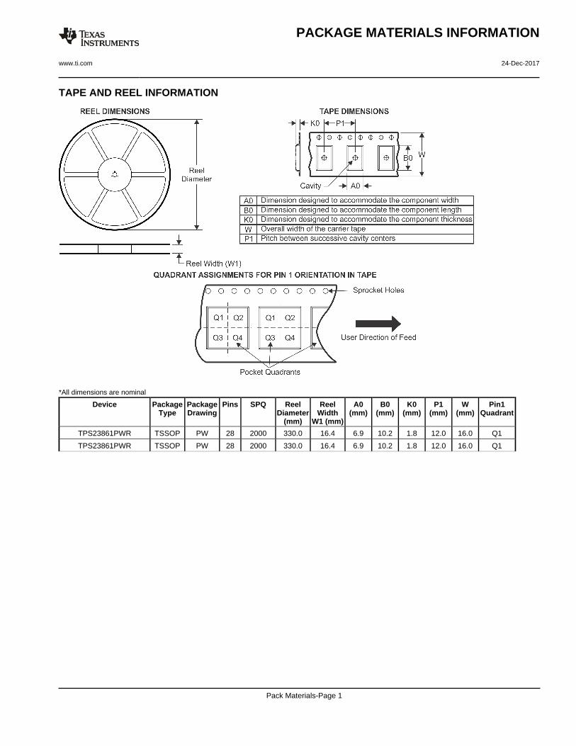
TAPE AND REEL INFORMATION
*All dimensions are nominal
Device PackageType
PackageDrawing
Pins SPQ ReelDiameter
(mm)
ReelWidth
W1 (mm)
A0(mm)
B0(mm)
K0(mm)
P1(mm)
W(mm)
Pin1Quadrant
TPS23861PWR TSSOP PW 28 2000 330.0 16.4 6.9 10.2 1.8 12.0 16.0 Q1
TPS23861PWR TSSOP PW 28 2000 330.0 16.4 6.9 10.2 1.8 12.0 16.0 Q1
PACKAGE MATERIALS INFORMATION
www.ti.com 24-Dec-2017
Pack Materials-Page 1

*All dimensions are nominal
Device Package Type Package Drawing Pins SPQ Length (mm) Width (mm) Height (mm)
TPS23861PWR TSSOP PW 28 2000 367.0 367.0 38.0
TPS23861PWR TSSOP PW 28 2000 367.0 367.0 38.0
PACKAGE MATERIALS INFORMATION
www.ti.com 24-Dec-2017
Pack Materials-Page 2
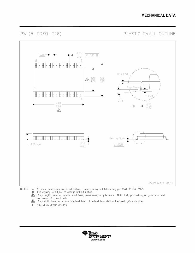


IMPORTANT NOTICE
Texas Instruments Incorporated (TI) reserves the right to make corrections, enhancements, improvements and other changes to itssemiconductor products and services per JESD46, latest issue, and to discontinue any product or service per JESD48, latest issue. Buyersshould obtain the latest relevant information before placing orders and should verify that such information is current and complete.TI’s published terms of sale for semiconductor products (http://www.ti.com/sc/docs/stdterms.htm) apply to the sale of packaged integratedcircuit products that TI has qualified and released to market. Additional terms may apply to the use or sale of other types of TI products andservices.Reproduction of significant portions of TI information in TI data sheets is permissible only if reproduction is without alteration and isaccompanied by all associated warranties, conditions, limitations, and notices. TI is not responsible or liable for such reproduceddocumentation. Information of third parties may be subject to additional restrictions. Resale of TI products or services with statementsdifferent from or beyond the parameters stated by TI for that product or service voids all express and any implied warranties for theassociated TI product or service and is an unfair and deceptive business practice. TI is not responsible or liable for any such statements.Buyers and others who are developing systems that incorporate TI products (collectively, “Designers”) understand and agree that Designersremain responsible for using their independent analysis, evaluation and judgment in designing their applications and that Designers havefull and exclusive responsibility to assure the safety of Designers' applications and compliance of their applications (and of all TI productsused in or for Designers’ applications) with all applicable regulations, laws and other applicable requirements. Designer represents that, withrespect to their applications, Designer has all the necessary expertise to create and implement safeguards that (1) anticipate dangerousconsequences of failures, (2) monitor failures and their consequences, and (3) lessen the likelihood of failures that might cause harm andtake appropriate actions. Designer agrees that prior to using or distributing any applications that include TI products, Designer willthoroughly test such applications and the functionality of such TI products as used in such applications.TI’s provision of technical, application or other design advice, quality characterization, reliability data or other services or information,including, but not limited to, reference designs and materials relating to evaluation modules, (collectively, “TI Resources”) are intended toassist designers who are developing applications that incorporate TI products; by downloading, accessing or using TI Resources in anyway, Designer (individually or, if Designer is acting on behalf of a company, Designer’s company) agrees to use any particular TI Resourcesolely for this purpose and subject to the terms of this Notice.TI’s provision of TI Resources does not expand or otherwise alter TI’s applicable published warranties or warranty disclaimers for TIproducts, and no additional obligations or liabilities arise from TI providing such TI Resources. TI reserves the right to make corrections,enhancements, improvements and other changes to its TI Resources. TI has not conducted any testing other than that specificallydescribed in the published documentation for a particular TI Resource.Designer is authorized to use, copy and modify any individual TI Resource only in connection with the development of applications thatinclude the TI product(s) identified in such TI Resource. NO OTHER LICENSE, EXPRESS OR IMPLIED, BY ESTOPPEL OR OTHERWISETO ANY OTHER TI INTELLECTUAL PROPERTY RIGHT, AND NO LICENSE TO ANY TECHNOLOGY OR INTELLECTUAL PROPERTYRIGHT OF TI OR ANY THIRD PARTY IS GRANTED HEREIN, including but not limited to any patent right, copyright, mask work right, orother intellectual property right relating to any combination, machine, or process in which TI products or services are used. Informationregarding or referencing third-party products or services does not constitute a license to use such products or services, or a warranty orendorsement thereof. Use of TI Resources may require a license from a third party under the patents or other intellectual property of thethird party, or a license from TI under the patents or other intellectual property of TI.TI RESOURCES ARE PROVIDED “AS IS” AND WITH ALL FAULTS. TI DISCLAIMS ALL OTHER WARRANTIES ORREPRESENTATIONS, EXPRESS OR IMPLIED, REGARDING RESOURCES OR USE THEREOF, INCLUDING BUT NOT LIMITED TOACCURACY OR COMPLETENESS, TITLE, ANY EPIDEMIC FAILURE WARRANTY AND ANY IMPLIED WARRANTIES OFMERCHANTABILITY, FITNESS FOR A PARTICULAR PURPOSE, AND NON-INFRINGEMENT OF ANY THIRD PARTY INTELLECTUALPROPERTY RIGHTS. TI SHALL NOT BE LIABLE FOR AND SHALL NOT DEFEND OR INDEMNIFY DESIGNER AGAINST ANY CLAIM,INCLUDING BUT NOT LIMITED TO ANY INFRINGEMENT CLAIM THAT RELATES TO OR IS BASED ON ANY COMBINATION OFPRODUCTS EVEN IF DESCRIBED IN TI RESOURCES OR OTHERWISE. IN NO EVENT SHALL TI BE LIABLE FOR ANY ACTUAL,DIRECT, SPECIAL, COLLATERAL, INDIRECT, PUNITIVE, INCIDENTAL, CONSEQUENTIAL OR EXEMPLARY DAMAGES INCONNECTION WITH OR ARISING OUT OF TI RESOURCES OR USE THEREOF, AND REGARDLESS OF WHETHER TI HAS BEENADVISED OF THE POSSIBILITY OF SUCH DAMAGES.Unless TI has explicitly designated an individual product as meeting the requirements of a particular industry standard (e.g., ISO/TS 16949and ISO 26262), TI is not responsible for any failure to meet such industry standard requirements.Where TI specifically promotes products as facilitating functional safety or as compliant with industry functional safety standards, suchproducts are intended to help enable customers to design and create their own applications that meet applicable functional safety standardsand requirements. Using products in an application does not by itself establish any safety features in the application. Designers mustensure compliance with safety-related requirements and standards applicable to their applications. Designer may not use any TI products inlife-critical medical equipment unless authorized officers of the parties have executed a special contract specifically governing such use.Life-critical medical equipment is medical equipment where failure of such equipment would cause serious bodily injury or death (e.g., lifesupport, pacemakers, defibrillators, heart pumps, neurostimulators, and implantables). Such equipment includes, without limitation, allmedical devices identified by the U.S. Food and Drug Administration as Class III devices and equivalent classifications outside the U.S.TI may expressly designate certain products as completing a particular qualification (e.g., Q100, Military Grade, or Enhanced Product).Designers agree that it has the necessary expertise to select the product with the appropriate qualification designation for their applicationsand that proper product selection is at Designers’ own risk. Designers are solely responsible for compliance with all legal and regulatoryrequirements in connection with such selection.Designer will fully indemnify TI and its representatives against any damages, costs, losses, and/or liabilities arising out of Designer’s non-compliance with the terms and provisions of this Notice.
Mailing Address: Texas Instruments, Post Office Box 655303, Dallas, Texas 75265Copyright © 2017, Texas Instruments Incorporated