Embed Size (px)
Citation preview

U
SLED1
SPMDriver
V
W
MCOM
SLED1+
SLED1-
SLED2 SLED2-
SLED2+
TLT
TLT+
TLT-
FCS FCS-
FCS+
TRK
TRK+
TRK-
LOAD LOAD-
LOAD+
5 V
5 V
5 V
5 V
5 V
5 V
5 V
SPI
5 VTPIC2030
1PX V output
DCDCV3P3
10 mF
REGOUT
REGFB
1.x/3.3 Voutput
3.3 V
Con
trol
ler
Product
Folder
Order
Now
Technical
Documents
Tools &
Software
Support &Community
An IMPORTANT NOTICE at the end of this data sheet addresses availability, warranty, changes, use in safety-critical applications,intellectual property matters and other important disclaimers. PRODUCTION DATA.
TPIC2030SLIS171 –DECEMBER 2015
TPIC2030 Serial I/F Controlled 7-Channel Motor-Driver With 1-Channel Step DownRegulator
1
1 Features1• Serial Peripheral Interface
– Maximum Read/Write 35 MHz– 3.3-V Digital I/O
• Actuator and Motor Driver– PWM Control With H-Bridge Output– Focus / Tracking / Tilt Actuator Driver With 12-
Bit DAC Control– Sled Motor Drivers With Current Mode, 10-Bit
DAC Control– Load Driver With 12-Bit DAC Control– End Position Sensing for Sled Without Position
Sensor• Spindle Motor Driver
– Integrated Spindle Current Sense Resistor– Sensor-Less: Rotor Position Sense by Motor
BEMF– 12-Bit Spindle DAC– Quick Stop by Automatic Controlled Brake
(Auto Short Brake)– LS Mode: Restricted to 25% of Normal Speed
• On-Chip Thermometer (15°C to 165°C/1.2°C)• Software Controlled Switch for LED Driver With
0.1-A OCP• Switch
– CSW: Low RDS(ON) Current Switch WithSelectable OCP Limit (Supposing Use <0.2 A)
– LED: Software Control Current Output PortWith 0.1-A OCP
• DC-DC Converter– Pin Selectable Conversion Voltage 1.0 V/ 1.2
V/ 1.5 V/ 3.3 V (or Disable)– Improved Efficiency at Low Current With
Discontinuous Regulation Mode• Protection
– Individual Thermal Protect Circuit onLED/CSW, Switch, DCDC Converter, SPM,and Actuator
– Overcurrent Protection– Undervoltage Lockout (UVLO) and
Overvoltage Protection (OVP)
2 Applications• DVD Player• CD Player• Optical Disk Drive
3 DescriptionTPIC2030 is very-low noise type motor driver ICsuitable for slim or ultra-slim DVD reader/writer. Theintegrated current sense resistance for the spindlemotor reduces cost and board area in designs. TheTPIC2030 is an integrated solution for driving thespindle motor, sled motor, load motor, and Focus /Tracking / Tilt actuators in an optical disk drive. It alsointegrates a synchronous DC-DC converter to supply1.0 or 3.3 V. The discontinuous mode regulationfeature on the DC-DC converter improves efficiencyat low power consumption.
Device Information(1)
PART NUMBER PACKAGE BODY SIZE (NOM)TPIC2030DBT TSSOP (44) 11.10 mm × 4.40 mm
(1) For all available packages, see the orderable addendum atthe end of the data sheet.
Simplified Block Diagram

2
TPIC2030SLIS171 –DECEMBER 2015 www.ti.com
Product Folder Links: TPIC2030
Submit Documentation Feedback Copyright © 2015, Texas Instruments Incorporated
Table of Contents1 Features .................................................................. 12 Applications ........................................................... 13 Description ............................................................. 14 Revision History..................................................... 25 Description (continued)......................................... 36 Pin Configuration and Functions ......................... 37 Specifications......................................................... 5
7.1 Absolute Maximum Ratings ...................................... 57.2 ESD Ratings.............................................................. 57.3 Recommended Operating Conditions....................... 57.4 Thermal Information .................................................. 67.5 Electrical Characteristics – Common Part ................ 77.6 Electrical Characteristics – Charge Pump Part......... 77.7 Electrical Characteristics – DC-DC Converter .......... 87.8 Electrical Characteristics – Spindle Motor Driver
Part............................................................................. 87.9 Electrical Characteristics – Sled Motor Driver Part... 97.10 Electrical Characteristics – Focus/
Tilt/Tracking/Driver Part ............................................. 97.11 Electrical Characteristics – Load Driver Part .......... 97.12 Electrical Characteristics – Current Switch Part ..... 97.13 Electrical Characteristics – LED Switch Part ........ 107.14 Electrical Characteristics – Thermometer Part ..... 107.15 Electrical Characteristics – Actuator Protection.... 107.16 Electrical Characteristics – Serial Port Voltage
Levels....................................................................... 10
7.17 Serial Port I/F Write Timing Requirements ........... 117.18 Serial I/F Read Timing Requirements................... 117.19 Typical Characteristics .......................................... 12
8 Detailed Description ............................................ 138.1 Overview ................................................................. 138.2 Functional Block Diagram ....................................... 148.3 Feature Description................................................. 158.4 Device Functional Modes........................................ 218.5 Programming........................................................... 248.6 Register Maps ......................................................... 26
9 Application and Implementation ........................ 439.1 Application Information............................................ 439.2 Typical Application ................................................. 52
10 Power Supply Recommendations ..................... 5411 Layout................................................................... 54
11.1 Layout Guidelines ................................................. 5411.2 Layout Example .................................................... 54
12 Device and Documentation Support ................. 5512.1 Device Support .................................................... 5512.2 Community Resources.......................................... 5512.3 Trademarks ........................................................... 5512.4 Electrostatic Discharge Caution............................ 5512.5 Glossary ................................................................ 55
13 Mechanical, Packaging, and OrderableInformation ........................................................... 55
4 Revision History
DATE REVISION NOTESDecember 2015 * Initial release.

1
2 LOAD+
LOAD–
3
4
5
SLED1+
SLED1–
SLED2+
SLED2–
6
7
8
9
CP2
CP1
CP3
W
10
SSZ
11
SCLK
U
12
SIMO
13
SOMI
V
44
14
SIOV
43
15 XRESET
MCOM
42
16
XFG
PGND_1
PGND_2
PGND_SPM
41
17
XMUTE
TRK-
40
18
TRK+
39
19
SWR_VSEL2
SWR_VSEL1
FCS–
38
20
FCS+
37
21 CV3P3A
36
22
TLT+
TLT–
35
23
AGND
P5V_SPM
P5V_1
34
24
GPOUT
LEDO
33
25
REGOUT
REGFB
32
26
P5V_SW
P5V_2
CSWO
31
27
30
28
PGND_SW
29–
3
TPIC2030www.ti.com SLIS171 –DECEMBER 2015
Product Folder Links: TPIC2030
Submit Documentation FeedbackCopyright © 2015, Texas Instruments Incorporated
5 Description (continued)Sensorless control using BEMF allows for self-starting and low-noise operation of the spindle motor withoutrequiring external sensors. In addition, the TPIC2030 has many built-in protection features including: spindledriver output current limiting, thermal shutdown, sled-end detection, and power-reset circuit. It also integrates athermometer to measure IC temperature.
6 Pin Configuration and Functions
DBT Package44-Pin TSSOP
Top View

4
TPIC2030SLIS171 –DECEMBER 2015 www.ti.com
Product Folder Links: TPIC2030
Submit Documentation Feedback Copyright © 2015, Texas Instruments Incorporated
(1) I: Input; O: Output; PS: Power; MISC: Miscellaneous
Pin FunctionsPIN
I/O (1) DESCRIPTIONNO. NAME
1 PGND_1 PS GND terminal2 PGND_SW PS GND terminal for DC-DC converters3 REGOUT O DC-DC converter switching output. Possible GPOUT pin in disable DC-DC4 P5V_SW PS Power supply terminal for DC-DC converters5 REGFB I Feedback input terminal for DC-DC converter6 SIOV PS Power supply terminal for serial port typical 3.3 V7 SWR_VSEL1 I Setting DC-DC converter output voltage8 SWR_VSEL2 I Setting DC-DC converter output voltage setting9 SSZ I SIO slave select low active input terminal10 SCLK I SIO serial clock input terminal11 SIMO I SIO slave input master output terminal12 SOMI O SIO slave output master input terminal13 XMUTE I XMUTE input terminal to disable driver output14 XFG O Motor speed signal output15 XRESET O Power on reset output. Internally pulled up to SIOV16 GPOUT O General-purpose output (test monitor)17 CP1 MISC Capacitance connection for charge pump18 CP2 MISC Capacitance connection for charge pump19 CP3 MISC Capacitance connection for charge pump20 AGND PS Ground terminal for internal logic21 CV3P3A MISC Capacitance terminal for internal 3.3-V regulator22 P5V_2 PS Power supply terminal23 PGND_2 PS GND terminal24 TLT+ O Tilt positive output terminal25 TLT– O Tilt negative output terminal26 FCS+ O Focus positive output terminal27 FCS– O Focus negative output terminal28 TRK+ O Tracking positive output terminal29 TRK– O Tracking negative output terminal30 PGND_SPM PS GND terminal for spindle driver31 V O V phase output terminal for spindle motor32 U O U phase output terminal for spindle motor33 W O W phase output terminal for spindle motor34 P5V_SPM PS Power supply terminal for Spindle driver35 P5V_1 PS Power supply terminal36 MCOM I Motor center tap connection37 CSWO O Power switch output for 5V OEIC in OPU38 LEDO O LED output terminal39 SLED1+ O Sled1 positive output terminal40 SLED1– O Sled1 negative output terminal41 SLED2+ O Sled2 positive output terminal42 SLED2– O Sled2 negative output terminal43 LOAD+ O Load positive output terminal44 LOAD– O Load negative output terminal
5
TPIC2030www.ti.com SLIS171 –DECEMBER 2015
Product Folder Links: TPIC2030
Submit Documentation FeedbackCopyright © 2015, Texas Instruments Incorporated
(1) Stresses beyond those listed under Absolute Maximum Ratings may cause permanent damage to the device. These are stress ratingsonly, which do not imply functional operation of the device at these or any other conditions beyond those indicated under RecommendedOperating Conditions. Exposure to absolute-maximum-rated conditions for extended periods may affect device reliability.
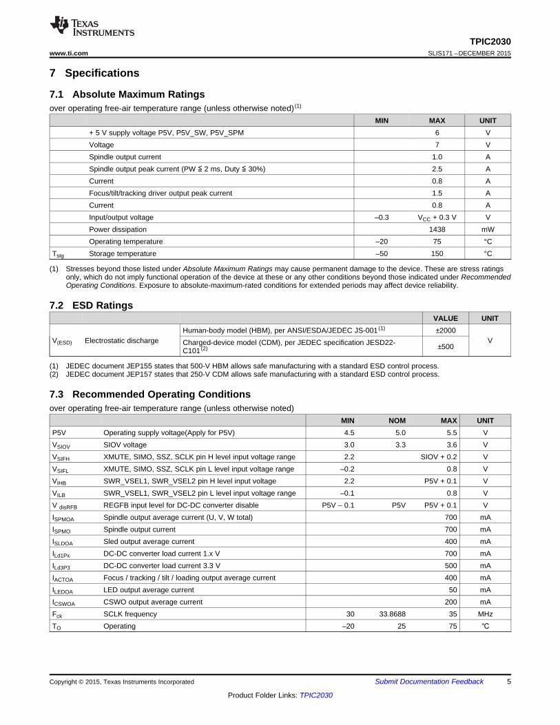
7 Specifications
7.1 Absolute Maximum Ratingsover operating free-air temperature range (unless otherwise noted) (1)
MIN MAX UNIT+ 5 V supply voltage P5V, P5V_SW, P5V_SPM 6 VVoltage 7 VSpindle output current 1.0 ASpindle output peak current (PW ≦ 2 ms, Duty ≦ 30%) 2.5 ACurrent 0.8 AFocus/tilt/tracking driver output peak current 1.5 ACurrent 0.8 AInput/output voltage –0.3 VCC + 0.3 V VPower dissipation 1438 mWOperating temperature –20 75 °C
Tstg Storage temperature –50 150 °C
(1) JEDEC document JEP155 states that 500-V HBM allows safe manufacturing with a standard ESD control process.(2) JEDEC document JEP157 states that 250-V CDM allows safe manufacturing with a standard ESD control process.
7.2 ESD RatingsVALUE UNIT
V(ESD) Electrostatic dischargeHuman-body model (HBM), per ANSI/ESDA/JEDEC JS-001 (1) ±2000
VCharged-device model (CDM), per JEDEC specification JESD22-C101 (2) ±500
7.3 Recommended Operating Conditionsover operating free-air temperature range (unless otherwise noted)
MIN NOM MAX UNITP5V Operating supply voltage(Apply for P5V) 4.5 5.0 5.5 VVSIOV SIOV voltage 3.0 3.3 3.6 VVSIFH XMUTE, SIMO, SSZ, SCLK pin H level input voltage range 2.2 SIOV + 0.2 VVSIFL XMUTE, SIMO, SSZ, SCLK pin L level input voltage range –0.2 0.8 VVIHB SWR_VSEL1, SWR_VSEL2 pin H level input voltage 2.2 P5V + 0.1 VVILB SWR_VSEL1, SWR_VSEL2 pin L level input voltage range –0.1 0.8 VV disRFB REGFB input level for DC-DC converter disable P5V – 0.1 P5V P5V + 0.1 VISPMOA Spindle output average current (U, V, W total) 700 mAISPMO Spindle output current 700 mAISLDOA Sled output average current 400 mAILd1Px DC-DC converter load current 1.x V 700 mAILd3P3 DC-DC converter load current 3.3 V 500 mAIACTOA Focus / tracking / tilt / loading output average current 400 mAILEDOA LED output average current 50 mAICSWOA CSWO output average current 200 mAFck SCLK frequency 30 33.8688 35 MHzTO Operating –20 25 75

6
TPIC2030SLIS171 –DECEMBER 2015 www.ti.com
Product Folder Links: TPIC2030
Submit Documentation Feedback Copyright © 2015, Texas Instruments Incorporated
(1) For more information about traditional and new thermal metrics, see the Semiconductor and IC Package Thermal Metrics applicationreport, SPRA953.
(2) The JEDEC specification low K (1 s) board design used to derive this data
7.4 Thermal Information
THERMAL METRIC (1)TPIC2030
UNITDBT (TSSOP)TBD PINS
RθJA Junction-to-ambient thermal resistance (2) 71.9 °C/WRθJC(top) Junction-to-case (top) thermal resistance 19.1 °C/WRθJB Junction-to-board thermal resistance 34.3 °C/WψJT Junction-to-top characterization parameter 0.5 °C/WψJB Junction-to-board characterization parameter 33.9 °C/WRθJC(bot) Junction-to-case (bottom) thermal resistance N/A °C/W
7
TPIC2030www.ti.com SLIS171 –DECEMBER 2015
Product Folder Links: TPIC2030
Submit Documentation FeedbackCopyright © 2015, Texas Instruments Incorporated
(1) Those are value as protection functions only, and stress beyond those listed under Recommended Operating Conditions may causepermanent damage to the device.
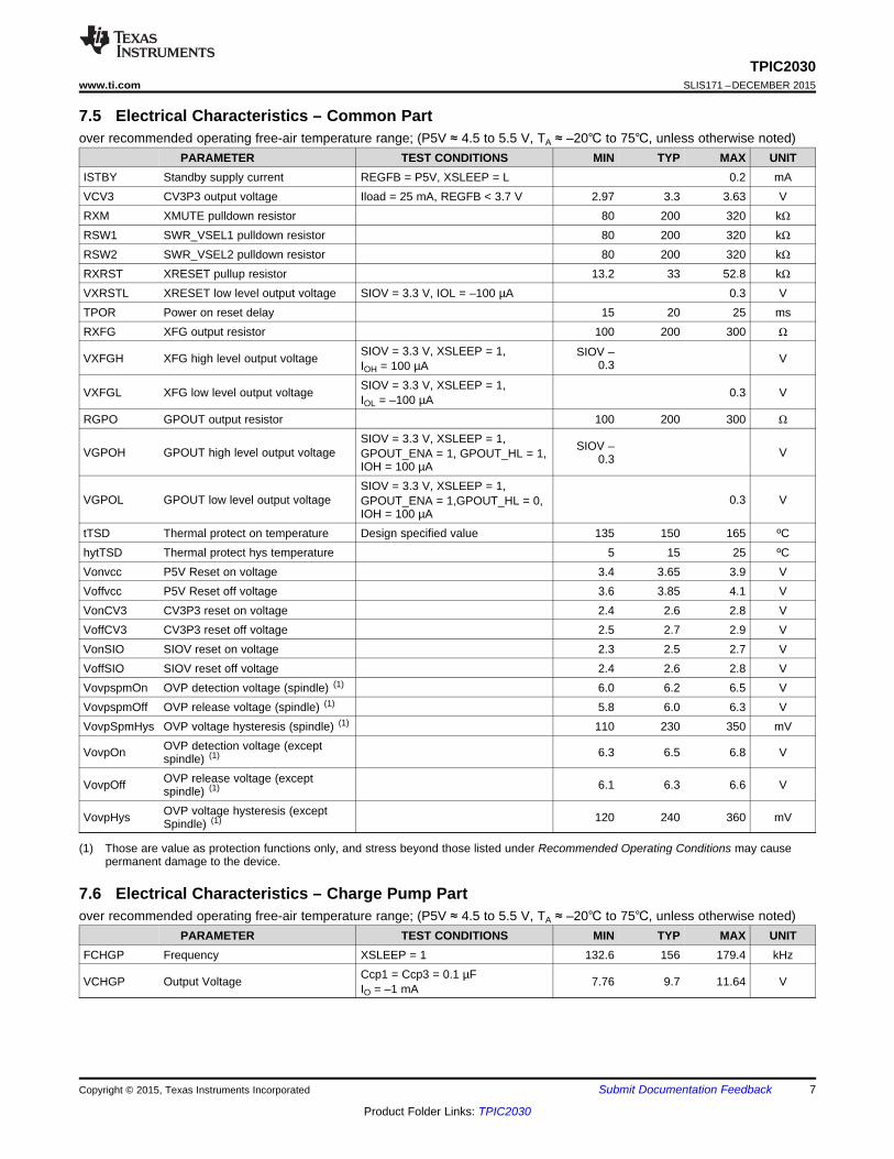
7.5 Electrical Characteristics – Common Partover recommended operating free-air temperature range; (P5V ≈ 4.5 to 5.5 V, TA ≈ –20 to 75, unless otherwise noted)
PARAMETER TEST CONDITIONS MIN TYP MAX UNITISTBY Standby supply current REGFB = P5V, XSLEEP = L 0.2 mAVCV3 CV3P3 output voltage Iload = 25 mA, REGFB < 3.7 V 2.97 3.3 3.63 VRXM XMUTE pulldown resistor 80 200 320 kΩRSW1 SWR_VSEL1 pulldown resistor 80 200 320 kΩRSW2 SWR_VSEL2 pulldown resistor 80 200 320 kΩRXRST XRESET pullup resistor 13.2 33 52.8 kΩVXRSTL XRESET low level output voltage SIOV = 3.3 V, IOL = –100 µA 0.3 VTPOR Power on reset delay 15 20 25 msRXFG XFG output resistor 100 200 300 Ω
VXFGH XFG high level output voltage SIOV = 3.3 V, XSLEEP = 1,IOH = 100 µA
SIOV –0.3 V
VXFGL XFG low level output voltage SIOV = 3.3 V, XSLEEP = 1,IOL = –100 µA 0.3 V
RGPO GPOUT output resistor 100 200 300 Ω
VGPOH GPOUT high level output voltageSIOV = 3.3 V, XSLEEP = 1,GPOUT_ENA = 1, GPOUT_HL = 1,IOH = 100 µA
SIOV –0.3 V
VGPOL GPOUT low level output voltageSIOV = 3.3 V, XSLEEP = 1,GPOUT_ENA = 1,GPOUT_HL = 0,IOH = 100 µA
0.3 V
tTSD Thermal protect on temperature Design specified value 135 150 165 ºChytTSD Thermal protect hys temperature 5 15 25 ºCVonvcc P5V Reset on voltage 3.4 3.65 3.9 VVoffvcc P5V Reset off voltage 3.6 3.85 4.1 VVonCV3 CV3P3 reset on voltage 2.4 2.6 2.8 VVoffCV3 CV3P3 reset off voltage 2.5 2.7 2.9 VVonSIO SIOV reset on voltage 2.3 2.5 2.7 VVoffSIO SIOV reset off voltage 2.4 2.6 2.8 VVovpspmOn OVP detection voltage (spindle) (1) 6.0 6.2 6.5 VVovpspmOff OVP release voltage (spindle) (1) 5.8 6.0 6.3 VVovpSpmHys OVP voltage hysteresis (spindle) (1) 110 230 350 mV
VovpOn OVP detection voltage (exceptspindle) (1) 6.3 6.5 6.8 V
VovpOff OVP release voltage (exceptspindle) (1) 6.1 6.3 6.6 V
VovpHys OVP voltage hysteresis (exceptSpindle) (1) 120 240 360 mV
7.6 Electrical Characteristics – Charge Pump Partover recommended operating free-air temperature range; (P5V ≈ 4.5 to 5.5 V, TA ≈ –20 to 75, unless otherwise noted)
PARAMETER TEST CONDITIONS MIN TYP MAX UNITFCHGP Frequency XSLEEP = 1 132.6 156 179.4 kHz
VCHGP Output Voltage Ccp1 = Ccp3 = 0.1 µFIO = –1 mA 7.76 9.7 11.64 V

8
TPIC2030SLIS171 –DECEMBER 2015 www.ti.com
Product Folder Links: TPIC2030
Submit Documentation Feedback Copyright © 2015, Texas Instruments Incorporated
(1) Those are value as protection functions only, and stress beyond those listed under Recommended Operating Conditions may causepermanent damage to the device.
(2) These value may fall in low temperature at selecting auto discontinuous mode (SWR_BSTAUTON = 1)
7.7 Electrical Characteristics – DC-DC Converterover recommended operating free-air temperature range; (P5V ≈ 4.5 to 5.5 V, TA ≈ –20 to 75, unless otherwise noted)
PARAMETER TEST CONDITIONS MIN TYP MAX UNIT
Rds1pxH High Side FET RDSON REGFB = 0 V REGOUT + 100 mA,+300 mA 0.42 0.62 Ω
Rds1pxL Low Side FET RDSON REGFB = 1.2 V REGOUT – 100mA, –300 mA 0.2 0.4 Ω
VO1p0 Output Voltage(1p0V) [SWR_VSEL2, SWR_VSEL1] = 10 0.95 1.0 1.05 VVO1p2 Output Voltage(1p2V) [SWR_VSEL2, SWR_VSEL1] = 01 1.14 1.2 1.26 VVO1p5 Output Voltage(1p5V) [SWR_VSEL2, SWR_VSEL1] = 11 1.425 1.5 1.575 VVO3p3 Output Voltage(3p3V) [SWR_VSEL2, SWR_VSEL1] = 00 3.13 3.3 3.47 V
Tdly1p2 Soft start time [SWR_VSEL2, SWR_VSEL1] = 01From P5V reset off to target 90% 0.66 0.82 0.98 ms
RdsO1p2 Output Pull down transistor Rdson REGFB = 1 V (at DC-DC enable) 616 880 1144 Ω
Fsw1px Switching frequency 2.125 2.5 2.875 MHzVrston1px Reset on voltage threshold level 75% 80% 85%Vrstoff1px Reset off voltage threshold level 85% 90% 95%VrstHys Reset off voltage threshold Hys 5% 10% 15%
PSRRDCDC PSRR ratioP5V_SW = 5 V + 200 mVpp,IO = 200 mA,F ≈ 100 kHz
26 – – dB
IovcDCDC Overcurrent protective level (1) (2)
[SWR_VSEL2, SWR_VSEL1] ≠ 00SWR_BSTAUTON = 0 1.3 1.85 2.4 A
[SWR_VSEL2, SWR_VSEL1] = 00SWR_BSTAUTON = 0 0.65 1.15 1.65 A
TMskovctpic mask time of over current protection(1) 0.7 1.0 1.3 ms
7.8 Electrical Characteristics – Spindle Motor Driver Partover recommended operating free-air temperature range; (P5V ≈ 4.5 to 5.5 V, TA ≈ –20 to 75, unless otherwise noted)
PARAMETER TEST CONDITIONS MIN TYP MAX UNIT
RttlSPM Total output resistanceHigh side + low side (IncldRcs) IOUT = 0.5 A 0.37 0.7 Ω
ResSPM Resolution 12 bitGnSPM Gain Magnification to 1.0 input 5.2 6.0 6.8 times
WidDZSPM Spindle dead bandForward 12h 52h 92hReverse –92h –52h –12h
WidDZSPMLS Spindle dead band (LS mode) –40h 0h 40h
SPMClim Current limit
SPM_RCOM_SEL = 00 801 890 979 mASPM_RCOM_SEL = 01 882 980 1078 mASPM_RCOM_SEL = 10 652 725 798 mASPM_RCOM_SEL = 11 705 784 863 mA

9
TPIC2030www.ti.com SLIS171 –DECEMBER 2015
Product Folder Links: TPIC2030
Submit Documentation FeedbackCopyright © 2015, Texas Instruments Incorporated
7.9 Electrical Characteristics – Sled Motor Driver Partover recommended operating free-air temperature range; (P5V ≈ 4.5 to 5.5 V, TA ≈ –20 to 75, unless otherwise noted)
PARAMETER TEST CONDITIONS MIN TYP MAX UNIT
RttlSLD Total output resistanceHigh side + low side IO = 0.5 A 0.8 1.2 Ω
ResSLD Resolution 10 bit
WidDZSLD input Dead bandForward 2h 1Fh 60hReverse –60h –1Fh –2h
GnSLD Sled current gainP5V = 5 VRL = 10 Ω, 2.2 mHVSLED = 7FFh
380 440 500 mA
VthEdetSLD END_DET BEMF threshold voltageSLEDENDTH<1:0> = 00 26 46 66 mVSLEDENDTH<1:0> = 01 42 82 122 mVSLEDENDTH<1:0> = 11 9 22 35 mV
7.10 Electrical Characteristics – Focus/ Tilt/Tracking/Driver Partover recommended operating free-air temperature range; (P5V ≈ 4.5 to 5.5 V, TA ≈ –20 to 75, unless otherwise noted)
PARAMETER TEST CONDITIONS MIN TYP MAX UNITRttlAct Total output resistance
High side + low sideIO = 0.5 A 0.7 1.1 Ω
ResACT Resolution 12 bitVOfstACT Each channel output offset voltage DAC_code = 000h –30 0 30 mVVOfstDACT Output offset voltage focus and tilt DIFF_TLT = 1 –50 0 50 mVGnDAct Difference gain focus and tilt DIFF_TLT = 1 –1 0 1 dbGnAct Gain magnification to 1.0 input 5.2 6 6.8 times
7.11 Electrical Characteristics – Load Driver Partover recommended operating free-air temperature range; (P5V ≈ 4.5 to 5.5 V, TA ≈ –20 to 75, unless otherwise noted)
PARAMETER TEST CONDITIONS MIN TYP MAX UNIT
RttlLOD Total output resistanceHigh side + low side IO = 0.5 A 0.7 1.1 Ω
ResLOD Resolution 12 bitGnLOD Gain Magnification to 1.0 input 5.2 6 6.8 times
WidDZLOD Dead bandForward 20hReverse –21h
TocpLOD Output 100% limit time LOAD_05CH = 0 0.64 0.8 0.96 s
IocpLOD Overcurrent protective Level
LOAD_05CH = 1 atLoad_OCP_IUP = 0 120 240 360 mA
LOAD_05CH = 1 atLoad_OCP_IUP = 1 215 430 645 mA
DlyocpLOD Overcurrent protection delay time LOAD_05CH = 1 0.64 0.8 0.96 s
7.12 Electrical Characteristics – Current Switch Partover recommended operating free-air temperature range; (P5V ≈ 4.5 to 5.5 V, TA ≈ –20 to 75, unless otherwise noted)
PARAMETER TEST CONDITIONS MIN TYP MAX UNITRdsCSW Rds(on) IO = 0.2 A 200 500 mΩ
IlmtCSW Current limit threshold level 0.25 0.5 0.75 AThlCSW Protection hold time 1.47 1.6 2.0 ms

10
TPIC2030SLIS171 –DECEMBER 2015 www.ti.com
Product Folder Links: TPIC2030
Submit Documentation Feedback Copyright © 2015, Texas Instruments Incorporated
7.13 Electrical Characteristics – LED Switch Partover recommended operating free-air temperature range; (P5V ≈ 4.5 to 5.5 V, TA ≈ –20 to 75, unless otherwise noted)
PARAMETER TEST CONDITIONS MIN TYP MAX UNITRdsLED Rds(on) IO = 10 mA 4.4 10 Ω
IlmtLED Current limit threshold level P5V = 5 V 0.055 0.1 0.145 AThlLED Protection hold time 0.35 0.4 0.66 ms
7.14 Electrical Characteristics – Thermometer Partover recommended operating free-air temperature range; (P5V ≈ 4.5 to 5.5 V, TA ≈ –20 to 75, unless otherwise noted)
PARAMETER TEST CONDITIONS MIN TYP MAX UNITResTEMP Resolution 7 bit
TEMPrng Temperature rangeCHIPTEMP[6:0] = 00 8 15 22
°CCHIPTEMP[6:0] = 7Fh 155 165 175
FTEMP Update cycle 8 10 12 KHz
7.15 Electrical Characteristics – Actuator Protectionover recommended operating free-air temperature range; (P5V ≈ 4.5 to 5.5 V, TA ≈ –20 to 75, unless otherwise noted)
PARAMETER TEST CONDITIONS MIN TYP MAX UNITTintACTTEMP Update cycle 21 26 31 ms
(1) Specified by design
7.16 Electrical Characteristics – Serial Port Voltage Levelsover recommended operating free-air temperature range; (P5V ≈ 4.5 to 5.5 V, TA ≈ –20 to 75, unless otherwise noted)
PARAMETER TEST CONDITIONS MIN TYP MAX UNIT
SOMI High-level output voltage, VOH IOH = 1 mA 80 %SIOV V
SOMI Low-level output voltage, VOL IOL = 1 mA 20%SIOV V
SIMO High-level input voltage, VIH70%
SIOV V
SIMO Low level input voltage, VIL20%
SIOV V
SIMO Input rise/fall time 10% → 90% SIOV 3.5 nsSOMI Output rise/fall time (1) Cload = 30 pF,10% 90% SIOV 10 nsSCLK Internal pulldown resistance 80 200 320 kΩSSZ Internal pullup resistance 80 200 320 kΩ

Tsl
Hi -Z
R
TsensFck
Tckl
TdsTdhTckh
Trdly Tsendl
Tsenh
Trls
SSZ
SCLK
SIMO
SOMI
Tsens
Tckh
Tsl
Tsenh
Tckl
Tds Tdh
Hi-Z
Fck
SSZ
SCLK
SIMO
SOMI
11
TPIC2030www.ti.com SLIS171 –DECEMBER 2015
Product Folder Links: TPIC2030
Submit Documentation FeedbackCopyright © 2015, Texas Instruments Incorporated
7.17 Serial Port I/F Write Timing RequirementsMIN NOM MAX UNIT
Fck SCLK clock frequency SIOV = 3.3 V 35 MHztckl SCLK low time 11 nstckh SCLK high time 11 nstsens SSZ setup time 7 nstsenh SSZ hold time 7 nstsl SSZ disable high time 11 nstds SIMO setup time (Write) 7 nstdh SIMO hold time (Write) 7 ns
7.18 Serial I/F Read Timing RequirementsMIN NOM MAX UNIT
Fck SCLK clock frequency SIOV = 3.3 V 35 MHztckl SCLK low time 11 nstckh SCLK high time 11 nstsens SSZ setup time 7 nstsenh SSZ hold time 7 nstsl SSZ disable high time 11 nstds SIMO setup time (Write) 7 nstdh SIMO hold time (Write) 7 nstrdly SOMI delay time (Read) CLOAD = 10 pF, SIOV = 3.3 V 2 9 nstsendl SOMI hold time (Read) CLOAD = 10 pF, SIOV = 3.3 V 2 9 ns
trls SOMI release time (Read) CLOAD = 10 pF, SIOV = 3.3 VFrom SSZ rise to SOMI HIZ 0 9 ns
Figure 1. Serial Port Write Timing
Figure 2. Serial Port Read Timings

DAC Code
Du
ty C
yc
le (
%)
-3000 -2000 -1000 0 1000 2000 3000
0
20
40
60
80
100
120
D001
FCS
FCS+
DAC Code
Du
ty C
yc
le (
%)
-3000 -2000 -1000 0 1000 2000 3000
0
20
40
60
80
100
120
D002
TLT
TLT+
12
TPIC2030SLIS171 –DECEMBER 2015 www.ti.com
Product Folder Links: TPIC2030
Submit Documentation Feedback Copyright © 2015, Texas Instruments Incorporated
7.19 Typical Characteristics
Figure 3. DAC Code vs Duty Cycle for FCS Outputs Figure 4. DAC Code vs Duty Cycle for TLT Outputs
13
TPIC2030www.ti.com SLIS171 –DECEMBER 2015
Product Folder Links: TPIC2030
Submit Documentation FeedbackCopyright © 2015, Texas Instruments Incorporated
8 Detailed Description
8.1 OverviewTPIC2030 is low noise type motor driver IC suitable for 5V optical disk drives. The 7-channel driver IC controlledby serial I/F is optimum for driving a spindle motor, a sled motor (stepping motor applicable), a load motor, andFocus / Tracking / Tilt actuators. The integrated current sense resistance for spindle motor current measurementreduces drive system cost. The spindle motor driver part uses integrated sensorless logic to attain very low-noiseoperation during startup and runtime. By using BEMF feedback, external sensors, such as a Hall device, are notneeded to carry out self-starting by the starting circuit or perform position detection. By using the efficient PWMdrivers, low-power operation can be achieved by controlling the PWM outputs. Dead zone less control is possiblefor a Focus / Tracking / Tilt actuator driver. In addition, the spindle part output current limiting circuit, the thermalshut down circuit, and the sled end-detection circuit offer protection for all actuators and motors.

SSZW
V
U
MCOM
AG
ND
CP
1
CP
2
CP
3
TRK+
TRK–
FCS+
TLT+
SOM I
SIM O
P5
V_
2
XFG
SCLK
LOAD+
P5
V_
SP
M
PGND_SW
XRESET
LEDO
CV3P3V
SIOV
XM UTE
GPOUT
5 V
CSWO
LED O
XFG
3.3 V
3.3 V
InterLock
XRESET
GPOUT
0.1 µ
SWR_ VSEL2
SWR_ VSEL1
5 V5 V
P5
V_
1
SLED2+
LOAD–
BEM F
SPM
REGFB
REGOUT
5 V
P5V_ SW5 V
1.x/3.3V
10 µ10 µ 0.1 µ
2.2 µH
Dig ital Core
SLED END
Detection
CSW
LED
int 3.3 VRegulator
P5V
P5V
P5V
ENDDET_ ENA
SLD_ ENA
FCS_ ENA
TRK_ ENA
CSW _ ON
LED_ ON
Pow erMonitor
SIOV SIOV
20
0 k
20
0 k
20
0 k
20
0 k
20
0 k
33 k
10 V(P5Vx2)
LOAD_ ENA
10 µ
pw r FET
XSLEEP
3.3 V
pw r FET
pw r FET
pw r FET
pw r FET
pw r FET
pw r FET
CSWO
5 V
0.1 µ 0.1 µ 0.1 µ10 µ0.1 µ
10 µ10 µ
PGND_SPM
Pre-driver
SPM_RCOM
SPM_ENA
ChargePump
SPM LogicDAC PWM
Analog
TPIC2030
I-F/B
F/B
F/B
F/B
F/B
I-F/B
Current Limit
Pre-driver
Detector
SSZ
SCLK
Pre-driver
Pre-driver
Pre-driver
Pre-driver
Pre-driver
ACTTEMPTH>0
On ChipThermometer
PG
ND
_1-2
SP
I I/F
AC
TT
EM
P
DC-DCControl
SLED1+
20
0 k
SLD_ ENA
TLT_ENA
FCS–
SLED1–
SLED2–
TLT–
DAC PWM
DAC PWM
DAC PWM
DAC PWM
DAC PWM
SIMO
SOMI
14
TPIC2030SLIS171 –DECEMBER 2015 www.ti.com
Product Folder Links: TPIC2030
Submit Documentation Feedback Copyright © 2015, Texas Instruments Incorporated
8.2 Functional Block Diagram

15
TPIC2030www.ti.com SLIS171 –DECEMBER 2015
Product Folder Links: TPIC2030
Submit Documentation FeedbackCopyright © 2015, Texas Instruments Incorporated
8.3 Feature Description
8.3.1 Protection FunctionsTPIC2030 has five protection features, under voltage lock out (UVLO), over voltage protection (OVP), shortcircuit protection (SCP), thermal protection (TSD), and actuator temperature protection (ACTTIMER) in order toprotect target equipment. A protect behavior differ by generated events.
8.3.1.1 Undervoltage Lockout (UVLO)Power faults are reported in the UVLOMon register. Each UVLOMon bit will be initialized to zero upon a coldpower up.
After a fault is detected the appropriate fault bit will be latched high. Writing to the RST_ERRFLG (REG77) willclear all UVLOMon bits. The power device faults and actions are summarized in Table 1.
Table 1. Power Fault Monitor
FAULT TYPE LATCHEDREGISTER XRESET CRITERIA SPM ACTUATOR DC-DC
P5V under voltage UVLO_P5V Yes <3.7 V Hi-Z Hi-ZREGOUT = Hi-ZREGFB = GND(enable DC-DC)
Internal 3.3 V under voltage UVLO_INT3P3 Yes <2.6 V Hi-Z Hi-Z Hi-ZDC-DC output under voltage UVLO_SWR Yes <80% Hi-Z Hi-ZSIOV under voltage UVLO_SIOV Yes <2.5 V Hi-Z Hi-Z
P5V over voltage OVP_P5V>6.2 V Brake – –>6.5 V Hi-Z Hi-Z Hi-Z
8.3.1.2 Overvoltage Protection (OVP)Over voltage protect function is aimed to protect the unit from the supplying hi-voltage.
When the supply voltage exceeds 6.5 V, all driver and DC-DC converter output goes Hi-Z. When the supplyvoltage falls below typical 6.2 V, (6.0 V for SPM) all output start to operate again. The OVP and POR (XRESET)function is not interlocking. However, DC-DC converter output falls by Hi-Z operations, output voltage falls to80% then XRESET signal goes low.
Moreover, when power supply exceeds 6.2 V, especially SPM enter short brake mode. This operation is offeredsupposing a voltage rising by motor BEMF of the high velocity revolution.
This function is for insurance, so it can not assure that the device is safety in the condition. Because the absolutemaximum ratings range of the supply voltage is 6 V. When this function works, the feed back terminals are notshorted to GND.
Figure 5 shows the behavior of over voltage protection.

6.5 V
6.3 V
6.2 V
6.0 V
Actuator
SPM
DCDC
Short Brake Hi-Z
LED/CSW
5-Vsupp ly
Hi-Z
16
TPIC2030SLIS171 –DECEMBER 2015 www.ti.com
Product Folder Links: TPIC2030
Submit Documentation Feedback Copyright © 2015, Texas Instruments Incorporated
Figure 5. Overvoltage Protection
8.3.1.3 Overcurrent Protection (OCP)The over current protect function serve to protect the device from break down by large current. The OCP isprovided for four circuit blocks, and each threshold are on Table 2.
Table 2. OCP ThresholdBLOCK DETECTION CURRENT MONITOR TIME PROTECTION TIME LATCHED FLAG
DC-DC converter 1850 mA (1.x V)1200 mA (3.3 V)
1 ms Forever(P5V power recycle)
OCP_SWR
Load driver 1 channel Continue 100% duty 800 ms forever OCP_LOADLoad driver 0.5 channel 240 mA 800 ms forever OCP_LOADLED driver 100 mA 20 µs 0.4 ms OCP_LEDCSW driver 500 mA 20 µs 1.6 ms OCP_CSW
When the large current is detected on each block, device put the output FET to Hi-Z.
The amounts of currents and time have specified the detection threshold for every circuit block.
When OCP occurs, it returns automatically after expiring set Hi-Z period. However, it restricts, the POR isperformed at OCP for DC-DC converter. It keeps XRESET = L and does not return forever. It’s necessary powerON/OFF actuation in order to make it release.
OCPERR (REG7F) and OCP flag (REG7B) are set at OCP detection.

LOAD+
LOAD current
LOAD–
XRESET
0 mA
Hi-Z
800 ms
240 mA
LOAD+
LOAD current
LOAD–
XRESET
Hi-Z
100% duty
800 ms
0 mA
REGOUT
DCDC conv Load-I
DCDC output
XRESET
1.8 A(1xV) / 1.2 A(3.3 V)
0 mA
1 ms
Hi-Z
No release(until P5V supply recycle)
17
TPIC2030www.ti.com SLIS171 –DECEMBER 2015
Product Folder Links: TPIC2030
Submit Documentation FeedbackCopyright © 2015, Texas Instruments Incorporated
8.3.1.3.1 OCP for DC-DC Converter
Figure 6. Overcurrent Protection DC-DC Converter
8.3.1.3.2 OCP for Load Driver
Figure 7. Overcurrent Protection Load 1-Channel
Figure 8. Overcurrent Protection Load 0.5-Channel

detect 1.6 µs
1.6 ms
Hi-Z
Short to GND
Hi-Z
VDAC set
Driver current
Driver voltage
XRESET
CSW current
500 m A
XRESET
CSW _ ON
CSW voltage
0 m A
20 µs
1.6 ms
Hi-Z
LED current
100 mA
XRESET
LED_ ON
LED voltage
0 mA
20 µs
0.4 ms
Hi-Z Hi-Z Hi-Z
18
TPIC2030SLIS171 –DECEMBER 2015 www.ti.com
Product Folder Links: TPIC2030
Submit Documentation Feedback Copyright © 2015, Texas Instruments Incorporated
8.3.1.3.3 OCP for LED Driver
Figure 9. Overcurrent Protection LED Driver
8.3.1.3.4 OCP for CSW
Figure 10. Overcurrent Protection Current Switch
8.3.1.3.4.1 Short Circuit Protection (SCP)
SCP function always monitors the output voltage of high-side and low-side FET of output driver, and when thesetting voltage is not outputted, it recognizes as SCP and changed output Hi-Z. It returns to the original stateautomatically 1.6 ms after.
Table 3. SCP ConditionBLOCK FUNCTION DETECTION CONDITION DETECT TIME HI-Z HOLD TIME
SPM driver SCP Monitor driver output voltageHigh-side FET output V = GND
Low-side FET output V = Supply V
0.8 to 1.6 µs 1.6 msSled driverLoad driver
Actuator driver
Figure 11. Example of SCP (Driver Short to GND)

19
TPIC2030www.ti.com SLIS171 –DECEMBER 2015
Product Folder Links: TPIC2030
Submit Documentation FeedbackCopyright © 2015, Texas Instruments Incorporated
8.3.1.4 Thermal Protection (TSD)The thermal protection (TSD) is a protect function which intercepts an output and suspends an operation whenthe IC temperature exceed a maximum permissible on a safety. TSD makes an output Hi-Z when thetemperature rises up and a threshold value is exceeded. There are two levels for threshold Alert and Trip. Alarmis given by status register TSD_FAULT_ on Alert level with 135°C. It continues rising up temperature, the registerTSD_ is set at 150°C and the driver output changes HI-Z. If temperature falls and is reached 135 degrees, it willoutput again.
TPIC2030 has total 11 temperature sensors in each circuit block. Particular sensor is assigned to appropriatestatus flag in Table 4.
Table 4. Thermal Sensor AssignmentCIRCUIT ALERT (°C) TRIP (°C) RELEASE (°C) ALERT FLAG TRIP FLAG
U 135 150 135 TSD_FAULT_SPM TSD_SPMV 135 150 135 TSD_FAULT_SPM TSD_SPMW 135 150 135 TSD_FAULT_SPM TSD_SPM
TLT 135 150 135 TSD_FAULT_ACT TSD_ACTFCS 135 150 135 TSD_FAULT_ACT TSD_ACTTRK 135 150 135 TSD_FAULT_ACT TSD_ACT
SLED1 135 150 135 TSD_FAULT_ACT TSD_ACTSLED2 135 150 135 TSD_FAULT_ACT TSD_ACTLOAD 135 150 135 TSD_FAULT_ACT TSD_ACT
LED/CSW 135 150 135 TSD_FAULT_LEDCSW TSD_ LEDCSWDCDC 135 150 135 TSD_FAULT_SWR TSD_SWR
(1) The ACTTEMP data is updated on Register in ACTPROT_OFF = 0 and ACTTEMPTH > 0.
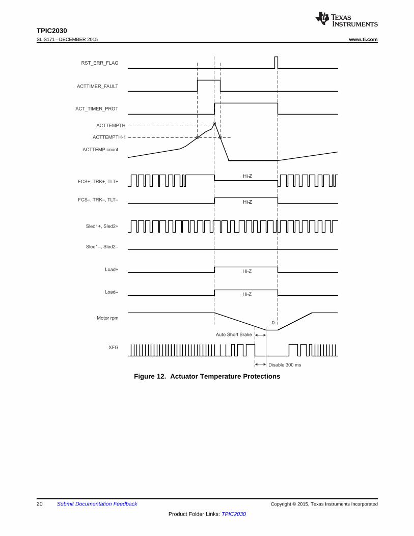
8.3.1.5 Actuator Temperature Protection (ACTTIMER)TPIC2030 has an actuator protect function named ACTTIMER. This function protects the IC by setting actuatorchannel output to HIZ when actuator coil current exceeds the specific value. This circuitry calculates heataccumulation to protect the actuators. When this function operates, sled1, 2 and load channel output will be Hi-Z,too. And spindle channel will be forced Auto short brake and disc motor will stop.
It’s able to know the protection has occurred by checking Fault register ACTTIMER_FAULT (REG7F) andACT_TIMER_PROT (REG78). ACTTIMER_FAULT has a character of advance notice, is set before detectingACT_TIMER_PROT. Once an ACT_TIMER_PROT is set, even if temperature falls, it will not release protectionautomatically. It is necessary to clear the flag by setting RST_ERR_FLAG (REG77) or setting 0 to ACTTEMPTH(REG72). ACTTIMER function is able to disable by setting H to ACTPROT_OFF (REG72) or setting 0 toACTTEMPTH (REG72).
In order to acquire the optimal value for ACTTEMPTH, you should set device into the condition of the detectionlevel, and reading the value of ACTTEMP. Because of the present value can be read from ACTTEMP (REG78).(1)
Hi-Z
Hi-Z
0
Disable 300 ms
Auto Short Brake
Hi-Z
Sled1–, Sled2–
Load+
Load–
Motor rpm
XFG
Hi-Z
Sled1+, Sled2+
FCS–, TRK–, TLT–
FCS+, TRK+, TLT+
ACTTEMP count
ACTTEMPTH-1
ACTTEMPTH
ACT_TIMER_PROT
ACTTIMER_FAULT
RST_ERR_FLAG
20
TPIC2030SLIS171 –DECEMBER 2015 www.ti.com
Product Folder Links: TPIC2030
Submit Documentation Feedback Copyright © 2015, Texas Instruments Incorporated
Figure 12. Actuator Temperature Protections

5.0 V
3.9 V
2.8 V
2.2 V
0 V
P5V>3.9 V && CV3P3>2.8 V
20 ms
CV3P3
P5V Supply
XRESETtime
5.0 V
3.9 V
2.8 V
2.2 V
0 V
P5V>3.9V && CV3P3>2.8V
1.6 ms 0.8 ms 20 ms
90% (REGOUT)
REGOUT
CV3P3
P5V SupplyLess than 10 ms
XRESETtime
21
TPIC2030www.ti.com SLIS171 –DECEMBER 2015
Product Folder Links: TPIC2030
Submit Documentation FeedbackCopyright © 2015, Texas Instruments Incorporated
8.4 Device Functional Modes
8.4.1 Power-On Reset (POR)
8.4.1.1 Power-Up SequencesIn TPIC2030, the normal sequence is to wait for 5-V supply to come up to 2.2 V. After 5 V establish, the internal3.3 V will start and wait until stabilize. Now the voltage monitors start to work and begin to look for the DC-DCconverter output. DC-DC converters stabilize the power up sequence finishes and the part starts to function.Once the part finishes all of its power up tasks, it takes XRESET high to indicate that the part is no longer inreset and ready to communicate to the outside world. All the DC-DC converter have soft-start features to avoidrush current and voltage over shoot. Each soft-start sequence takes about 0.8 ms.
Figure 13. POR (Enable DCDC)
Figure 14. POR (Disable DCDC)

(*1) DC-DC converter disable is REGFB>3.7 V
(*2) When exceed 6.5 V, DC-DC converter output
changed Hi-Z and output falling <80%.
Consequently force RESET event. (Released > 90%)
and CV3P3 > 2.7 V
and SIOV > 2.6 V
and DC-DC conv output > 90%
and P5V < 6.3 V (*2 )
P5V < 3.65 V
or CV3P3 < 2.6 V
or SIOV < 2.5 V
or DC-DC conv output < 80% (DC-DC enable)
or P5V > 6.5 V (*2)
or TSD > 150 degree (only TSD_SWR = 1)
or OCP_SWR = 1
20 ms
P5V > 3.85 V
and CV3P3 > 2.7 V
and SIOV > 2.6 V
and DC-DC conv Disable (*1)
TSD < 135 degree
RST_REGS = 1
SIF_TIMEOUTERR_MON = 1
OCP_SWR = 1
Hold XRESET
eset
P5V > 3.85 V
XRESET: High
Register Reset Register Valid Data
(Write Data)
XRESET: Low
Power on Reset
P5V
> 3.9 V
> 2.8 V
< 6.5 V
> 90%
SIOV
XRESET
REGFB
> 2.6 V
DC-DCREGOUT
DelayTimer
ThermalProtection
INT 3.3-VRegulator
P5V_SW
22
TPIC2030SLIS171 –DECEMBER 2015 www.ti.com
Product Folder Links: TPIC2030
Submit Documentation Feedback Copyright © 2015, Texas Instruments Incorporated
Device Functional Modes (continued)8.4.1.2 XRESETTPIC2030 is preparing XRESET pin in order to notify an own status to DSP. TPIC2030 set XRESET to L whenthe event which has a serious effect on DSP occurs such like the power failure, the over temperature and thedrop of DCDC converter output. If all the exception is removed, it will tell that XRESET pin would be set to H andit would be in the ready state. The POR (power-on reset) condition is shown in Figure 15. All the behavior ofXRESET is shown in Figure 16.
Figure 15. POR Block Diagram
Figure 16. XRESET Behavior

23
TPIC2030www.ti.com SLIS171 –DECEMBER 2015
Product Folder Links: TPIC2030
Submit Documentation FeedbackCopyright © 2015, Texas Instruments Incorporated
Device Functional Modes (continued)8.4.2 XMUTEIf XMUTE signal is inputted during operation, all the outputs will be suspended and the danger will be avoided.
TPIC2030 will turn off all enable bits, actuator (TLT_ENA/FCS_ENA/TRK_ENA), SPM_ENA, SLD_ENA,LOAD_ENA and CSW_ON when XMUTE input change to L. LOAD_ENA bit will be disabled only whenLOAD_05CH =1. Also log this event to error latch flag XMUTE_DETECT (REG79) and PWRERR (REG7F).
If XMUTE_NORST (REG7F) = 1, change of XMUTE will not influence to enable bits.

A4 A3 A2 A1 A0 D7 D6 D5 D4 D3 D2 D1 D0
Hi-Z
A6 A5 WSIMO
SCLK
SOMI
SSZ
C3 C2 C1 C0 D11 D10 D8D9 D7 D6 D5 D4 D3 D2 D1 D0
Hi-Z
SIMO
SCLK
SOMI
SSZ
24
TPIC2030SLIS171 –DECEMBER 2015 www.ti.com
Product Folder Links: TPIC2030
Submit Documentation Feedback Copyright © 2015, Texas Instruments Incorporated
8.5 Programming
8.5.1 Serial Port Functional DescriptionThe serial communication of TPIC2030 is based on a SPI communications protocol. TPIC2030 is put on theslave side.
All 16-bit transmission data is effective in SSZ=L period.
The bit stream sent through SIMO from a master (DSP) is latched to an internal shift register by the rising edgeof SCLK. All the data is transmitted in a total of 16-bit format of a command and data. A format has two types ofdata, 8 bits and 12 bits length. In order to access specific registers, an address and R/W flag are specified as acommand part. In addition, 12 bit data do not have R/W flag in the packet because DAC register ( =12bit dataform) are Write only. A transfer packet, command and data, is transmitted sequentially from MSB to LSB. Apacket is distinguished in MSB 2 bits of command. In the case of 11, it handles a packet for control registeraccess, and the other processed as a packet for a DAC data setting.
There are the following four kinds of serial-data communication packets.1. Write 12 bits DAC data (MSB two bit ≠ 11)2. Write 8 bits control register (MSB two bit = 11)3. Read 8 bits control register (MSB two bit = 11)4. Write 12 bits Focus DAC data+Read 8 bits status register at the same time (MSB two bit ≠ 11)
8.5.2 Write OperationFor write operation, DSP transmits 16 bit (command + address + data) data a bit every in an order from MSB.
Only the 16-bit data which means 16 SCLK sent from the master during SSZ=L becomes effective. If more than17 or less than 15 SCLK pulses are received during the time that SSZ is low, the whole packet will be ignored.For all valid write operations, the data of the shift register is latched into its designated internal register at risingedge of 16th SCLK. All internal register bits, except indicated otherwise, are reset to their default states uponpower-on-reset.
Figure 17. Write 12-Bits DAC Data
Figure 18. Write 8-Bits Control Register

C3 C2 C1 C0 D11 D10 D8D9 D7 D6 D5 D4 D3 D2 D1 D0SIMO
SCLK
D7 D6 D5 D4 D3 D2 D1 D0SOMIHi-Z
SSZ
D7 D6 D5 D4 D3 D2 D1 D0Hi-Z
RA4 A3 A2 A1 A0A6 A5SIMO
SCLK
SOMI
SSZ
25
TPIC2030www.ti.com SLIS171 –DECEMBER 2015
Product Folder Links: TPIC2030
Submit Documentation FeedbackCopyright © 2015, Texas Instruments Incorporated
Programming (continued)8.5.3 Read OperationDSP sends 8-bit header through SIMO, in order to perform Read operation. TPIC2030 will start to drive theSOMI line upon the eighth falling edge of SCLK and shift out eight data bits. The master DSP inputs 8-bits datafrom SOMI after the ninth rising edge of SCLK. There is optional read mode that SOMI data is advanced a halfclock cycle of SCLK. This mode becomes effective by setting ADVANCE_RD (REG74) = H.
Figure 19. Read 8-Bits Control Register
8.5.4 Write and Read OperationOptionally, the master DSP can read Status register during writing 12 bits DAC (Focus DAC) packet. It’s enabledby setting bit RDSTAT_ON_VFCS (REG74) = H.
Figure 20. Write 12-Bits Focus DAC Data + Read 8-Bits Status Data

In itial Value Set
Error latched Reg data
(REG78,79,7A,7B,7F[5:1])
XRESET = H
(TPIC2030 output)
P5V < 3.7V
or CV3P3 < 2.7V
or SIOV < 2.5V
or DCDC converter < 80%
or P5V> 6.5V
or RST_ REGS= 1
or SIF_ TIM EOUT_ ERR= 1
Reg ister Enable
W RITE_ ENABLE = 0
or XSLEEP = 0
Device Pow er On
Version Data
P5V< 2.0 V
or CV3P3 < 2.0 V
or RST_ ERR_ FLAG = 1
VDAC Reg data
(REG01-09) W rite(Vxxx)
SetValue
RST_ INDAC = 1
or XXX_ ENA = 0
Initial (000)
Control Reg data
(REG70 .. 7 F, 6D .. 6F)Driver Enab le
(REG70 xxx_ ENA, REG71 CSW _ ON)
W rite (1)XMUTE= L
(@ XMUTE_ NORST= 0) *
disab le (0)
enab le (1)
*disable LOAD_ENA only Load05_CH = 1
** SWR_xxx isnot influenced by XMUTE = L
P5V < 3.65 Vor CV3P3 < 2.6 Vor SIOV < 2.5 Vor DCDC converter < 80%or P5V > 6.5 Vor RST_REGS = 1or SIF_TIMEOUT_ERR = 1
P5V < 3.65 Vor CV3P3 < 2.6 Vor SIOV < 2.5 Vor DCDC converter < 80%or P5V > 6.5 Vor XMUTE = Lor SIF_TIMEOUT_ERR = 1or RST_REGS = 1
(REG7E)
(error occur, xmute = L)
26
TPIC2030SLIS171 –DECEMBER 2015 www.ti.com
Product Folder Links: TPIC2030
Submit Documentation Feedback Copyright © 2015, Texas Instruments Incorporated
8.6 Register MapsAll registers are in WRITE-protect mode after XRESET release. WRITE_ENA bit (REG76) = H is required beforewriting data in register.
8.6.1 Register State Transition
Figure 21. Register State Transition Chart

TPIC2030www.ti.com SLIS171 –DECEMBER 2015
27
Product Folder Links: TPIC2030
Submit Documentation FeedbackCopyright © 2015, Texas Instruments Incorporated
(1) TPIC2030 process as 0 even if set 1.
8.6.2 DAC Register (12-Bit Write Only)Two difference forms are prepared in 12-bit DAC register, and the forms can be selected by setting VDAC_MAPSW (REG74h).
Table 5. DAC Register (VDAC_MAPSW = 0)REG NAME F 11 10 9 8 7 6 5 4 3 2 1 000h N/A W N/A N/A N/A01h VTLT W VTLT[11] VTLT[10] VTLT[9] VTLT[8] VTLT[7] VTLT[6] VTLT[5] VTLT[4] VTLT[3] VTLT[2] VTLT[1] VTLT[0]02h VFCS W VFCS[11] VFCS[10] VFCS[9] VFCS[8] VFCS[7] VFCS[6] VFCS[5] VFCS[4] VFCS[3] VFCS[2] VFCS[1] VFCS[0]03h VTRK W VTRK[11] VTRK[10] VTRK[9] VTRK[8] VTRK[7] VTRK[6] VTRK[5] VTRK[4] VTRK[3] VTRK[2] VTRK[1] VTRK[0]04h VSLD1 W VSLD1[11] VSLD1[10] VSLD1[9] VSLD1[8] VSLD1[7] VSLD1[6] VSLD1[5] VSLD1[4] VSLD1[3] VSLD1[2] VSLD1[1] (1
)VSLD1[0]
(1)
05h VSLD2 W VSLD2[11] VSLD2[10] VSLD2[9] VSLD2[8] VSLD2[7] VSLD2[6] VSLD2[5] VSLD2[4] VSLD2[3] VSLD2[2] VSLD2[1](1)
VSLD2[0](1)
06h N/A W N/A N/A N/A07h N/A W N/A N/A N/A08h VSPM W VSPM[11] VSPM[10] VSPM[9] VSPM[8] VSPM[7] VSPM[6] VSPM[5] VSPM[4] VSPM[3] VSPM[2] VSPM[1] VSPM[0]09h VLOAD W VLOAD[11] VLOAD[10] VLOAD[9] VLOAD[8] VLOAD[7] VLOAD[6] VLOAD[5] VLOAD[4] VLOAD[3] VLOAD[2] VLOAD[1] VLOAD[0]0Ah N/A W N/A N/A N/A0Bh N/A W N/A N/A N/A

TPIC2030SLIS171 –DECEMBER 2015 www.ti.com
28
Product Folder Links: TPIC2030
Submit Documentation Feedback Copyright © 2015, Texas Instruments Incorporated
(1) TPIC2030 process as 0 even if set 1.
Table 6. DAC Register (VDAC_MAPSW = 1)REG NAME F 11 10 9 8 7 6 5 4 3 2 1 000h N/A W N/A N/A N/A01h VTLT W VTRK[11] VTRK[10] VTRK[9] VTRK[8] VTRK[7] VTRK[6] VTRK[5] VTRK[4] VTRK[3] VTRK[2] VTRK[1] VTRK[0]02h VFCS W VFCS[11] VFCS[10] VFCS[9] VFCS[8] VFCS[7] VFCS[6] VFCS[5] VFCS[4] VFCS[3] VFCS[2] VFCS[1] VFCS[0]03h VTRK W VTLT[11] VTLT[10] VTLT[9] VTLT[8] VTLT[7] VTLT[6] VTLT[5] VTLT[4] VTLT[3] VTLT[2] VTLT[1] VTLT[0]04h VSLD1 W VSLD1[11] VSLD1[10] VSLD1[9] VSLD1[8] VSLD1[7] VSLD1[6] VSLD1[5] VSLD1[4] VSLD1[3] VSLD1[2] VSLD1[1]
(1)VSLD1[0]
(1)
05h VSLD2 W VSLD2[11] VSLD2[10] VSLD2[9] VSLD2[8] VSLD2[7] VSLD2[6] VSLD2[5] VSLD2[4] VSLD2[3] VSLD2[2] VSLD2[1](1)
VSLD2[0](1)
06h VSPM W VSPM[11] VSPM[10] VSPM[9] VSPM[8] VSPM[7] VSPM[6] VSPM[5] VSPM[4] VSPM[3] VSPM[2] VSPM[1] VSPM[0]07h N/A W N/A N/A N/A08h N/A W N/A N/A N/A09h VLOAD W N/A VLOAD[11] VLOAD[10] VLOAD[9] VLOAD[8] VLOAD[7] VLOAD[6] VLOAD[5] VLOAD[4]0Ah N/A W N/A N/A N/A0Bh N/A W N/A N/A N/A

TPIC2030www.ti.com SLIS171 –DECEMBER 2015
29
Product Folder Links: TPIC2030
Submit Documentation FeedbackCopyright © 2015, Texas Instruments Incorporated
(1) VTRK and VLOAD is exclusive, using same DAC block
8.6.3 Control Register
Table 7. Control Register (8bit Read/Write) (1)
REG NAME F 7 6 5 4 3 2 1 0
70h DriverEna R/W TLT_ENA FCS_ENA TRK_ENA SPM_ENA SLD_ENA SWR_MD_BURST LOAD_ENA XSLEEP
71h FuncEna R/W SPM_LSMODE ENDDET_ENA SWR_BSTAUTON LED_ON CSW_ON TEMPMON_ENA TI reserved
72h ACTCfg R/W LOAD_O5CH_HIGH LOADPROT_OFF ACTPROT_OFF ACTTEMPTH
73h Parm0 R/W SIF_TIMEOUT_TH SLEDEND_HZTIME SLDENDTH SPM_RCOM_SEL XMUTE_NORST
74h OptSet R/W DIFF_TLT LOAD05_CH STATUS_ON_VFCS VSLD2_POL LOAD_OCP_IUP TI reserved SOMI_HIZ VDAC_MAPSW
75h Protect R/W TI reserved
76h WriteEna R/W WRITE_ENABLE TI reserved
77h ClrReg W RST_INDAC RST_REGS RST_ERR_FLAG TI reserved
78h ActTemp R TI reserved ACT_TIMER_PROT ACTTEMP
79h UVLOMon R TI reserved XMUTE_DETECT UVLO_P5V UVLO_INT3P3 UVLO_SIOV UVLO_SWR OVP_P5V
7Ah TsdMon R TSD_FAULT_SWR TSD_FAULT_SPM TSD_FAULT_ACT TSD_FAULT_LEDCSW TSD_SWR TSD_SPM TSD_ACT TSD_ LEDCSW
7Bh ProtMon R OCP_SWR OCP_LOAD OCP_LED OCP_CSW SCP_SPM SCP_SLED SCP_LOAD SCP_ACT
7Ch TempMon R CHIPTEMP_STATUS CHIPTEMP
7Dh Protect R TI reserved
7Eh Version R Version
7Fh Status R ACTTIMER_FAULT ENDDET SIF_TIMEOUTERR PWRERR TSDERR OCPSCPERR TSDFAULT FG
60h Protect R/W TI reserved
61h Protect R/W TI reserved
62h Protect R/W TI reserved
63h Protect R/W TI reserved
64h Protect R/W TI reserved
65h Protect R/W TI reserved FBSVR_SBRK_OFF TI reserved
66h Protect R/W TI reserved
6Ah Protect R/W TI reserved
6Ch Protect R/W TI reserved
6Dh DCCfg R/W TI reserved SWR_BST_HEFF TI reserved SWR_VOUTUP
6Eh UtilCfg R/W GPOUT_HL GPOUT_ENA TI reserved SWR_GPIO_CNTL TI reserved
6Fh MonitorSet R/W ACTTIMER_FLT_MON ENDDET_MON SIF_TIMEOUTERR_MON
PWRERR_MON TSDERR_MON OCPSCPERR_MON TSDFAULT_MON TI reserved

30
TPIC2030SLIS171 –DECEMBER 2015 www.ti.com
Product Folder Links: TPIC2030
Submit Documentation Feedback Copyright © 2015, Texas Instruments Incorporated
8.6.4 Detailed Description of Registers
8.6.4.1 REG01 12-bit DAC for Tilt (VDAC_MAPSW = 0)
Figure 22. Tilt (REG01)
15 14 13 12 11 10 9 8VTLT
w-0 w-0 w-0 w-0
7 6 5 4 3 2 1 0VTLT
w-0 w-0 w-0 w-0 w-0 w-0 w-0 w-0LEGEND: R/W = Read/Write; R = Read only; -n = value after reset
Table 8. Tilt (REG01) Field DescriptionsBit Field Type Default Description
11-0 VTLT w 0 Digital input code for Tilt.2’s compliment format 0x800(-2048) to 0x7ff(+2047)Output is changed by differential Tilt mode (REG74[7])TLT_OUT = VTLT* (6.0/2048) (DIFF_TLT=0)TLT_OUT = (VFCS-VTLT)* (6.0/2048) (DIFF_TLT=1)TLT_OUT shouldbe changed after writing VFCS.In DIFF_TLT mode (DIFF_TLT=1), TLT_OUT should be changed afterwriting VFCS.
8.6.4.2 REG02 12-bit DAC for Focus (VDAC_MAPSW = 0)
Figure 23. Focus (REG02)
15 14 13 12 11 10 9 8VFCS
w-0 w-0 w-0 w-0
7 6 5 4 3 2 1 0VFCS
w-0 w-0 w-0 w-0 w-0 w-0 w-0 w-0LEGEND: R/W = Read/Write; R = Read only; -n = value after reset
Table 9. Focus (REG02) Field DescriptionsBit Field Type Default Description
11-0 VFCS w 0 Digital input code for Focus.2’s compliment format 0x800(-2048) to 0x7ff(+2047)Output is changed by differential Tilt mode (REG74[7])FCS_OUT = VFCS × (6.0/2048) (DIFF_TLT=0)FCS_OUT = (VFCS+VTLT)* (6.0/2048) (DIFF_TLT=1)

31
TPIC2030www.ti.com SLIS171 –DECEMBER 2015
Product Folder Links: TPIC2030
Submit Documentation FeedbackCopyright © 2015, Texas Instruments Incorporated
8.6.4.3 REG03 12-bit DAC for Track (VDAC_MAPSW = 0)
Figure 24. Track (REG03)
15 14 13 12 11 10 9 8VTRK
w-0 w-0 w-0 w-0
7 6 5 4 3 2 1 0VTRK
w-0 w-0 w-0 w-0 w-0 w-0 w-0 w-0LEGEND: R/W = Read/Write; R = Read only; -n = value after reset
Table 10. Track (REG03) Field DescriptionsBit Field Type Default Description
11-0 VTRK w 0 Digital input code for Tracking.2’s compliment format 0x800(-2048) to 0x7ff(+2047)TRK_OUT = VTRK* (6.0/2048)
8.6.4.4 REG04 10bit DAC for Sled1 (VDAC_MAPSW = 0)
Figure 25. Sled1 (REG04)
15 14 13 12 11 10 9 8VSLD1
w-0 w-0 w-0 w-0
7 6 5 4 3 2 1 0VSLD1
w-0 w-0 w-0 w-0 w-0 w-0 w-0 w-0LEGEND: R/W = Read/Write; R = Read only; -n = value after reset
Table 11. Sled1 (REG04) Field DescriptionsBit Field Type Default Description
11-2 VSLD1 w 0 Digital input code for Sled1.2’s compliment format 0x800(-2048) to 0x7ff(+2047)Two bits on LSB, VSLD1[1:0], will be handled with zero.SLD1_OUT = VSLD1* (440mA/2048)
1-0 TI reserved
32
TPIC2030SLIS171 –DECEMBER 2015 www.ti.com
Product Folder Links: TPIC2030
Submit Documentation Feedback Copyright © 2015, Texas Instruments Incorporated
8.6.4.5 REG05 10bit DAC for Sled2 (VDAC_MAPSW = 0)
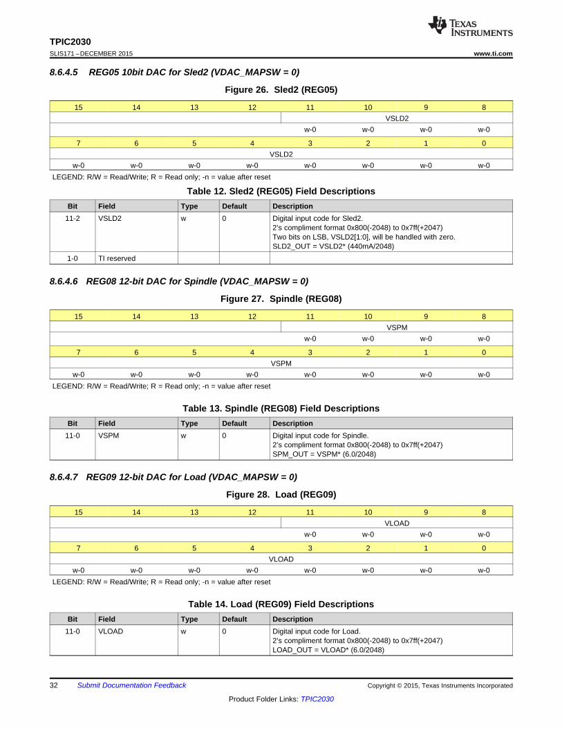
Figure 26. Sled2 (REG05)
15 14 13 12 11 10 9 8VSLD2
w-0 w-0 w-0 w-0
7 6 5 4 3 2 1 0VSLD2
w-0 w-0 w-0 w-0 w-0 w-0 w-0 w-0LEGEND: R/W = Read/Write; R = Read only; -n = value after reset
Table 12. Sled2 (REG05) Field DescriptionsBit Field Type Default Description
11-2 VSLD2 w 0 Digital input code for Sled2.2’s compliment format 0x800(-2048) to 0x7ff(+2047)Two bits on LSB, VSLD2[1:0], will be handled with zero.SLD2_OUT = VSLD2* (440mA/2048)
1-0 TI reserved
8.6.4.6 REG08 12-bit DAC for Spindle (VDAC_MAPSW = 0)
Figure 27. Spindle (REG08)
15 14 13 12 11 10 9 8VSPM
w-0 w-0 w-0 w-0
7 6 5 4 3 2 1 0VSPM
w-0 w-0 w-0 w-0 w-0 w-0 w-0 w-0LEGEND: R/W = Read/Write; R = Read only; -n = value after reset
Table 13. Spindle (REG08) Field DescriptionsBit Field Type Default Description
11-0 VSPM w 0 Digital input code for Spindle.2’s compliment format 0x800(-2048) to 0x7ff(+2047)SPM_OUT = VSPM* (6.0/2048)
8.6.4.7 REG09 12-bit DAC for Load (VDAC_MAPSW = 0)
Figure 28. Load (REG09)
15 14 13 12 11 10 9 8VLOAD
w-0 w-0 w-0 w-0
7 6 5 4 3 2 1 0VLOAD
w-0 w-0 w-0 w-0 w-0 w-0 w-0 w-0LEGEND: R/W = Read/Write; R = Read only; -n = value after reset
Table 14. Load (REG09) Field DescriptionsBit Field Type Default Description
11-0 VLOAD w 0 Digital input code for Load.2’s compliment format 0x800(-2048) to 0x7ff(+2047)LOAD_OUT = VLOAD* (6.0/2048)
33
TPIC2030www.ti.com SLIS171 –DECEMBER 2015
Product Folder Links: TPIC2030
Submit Documentation FeedbackCopyright © 2015, Texas Instruments Incorporated
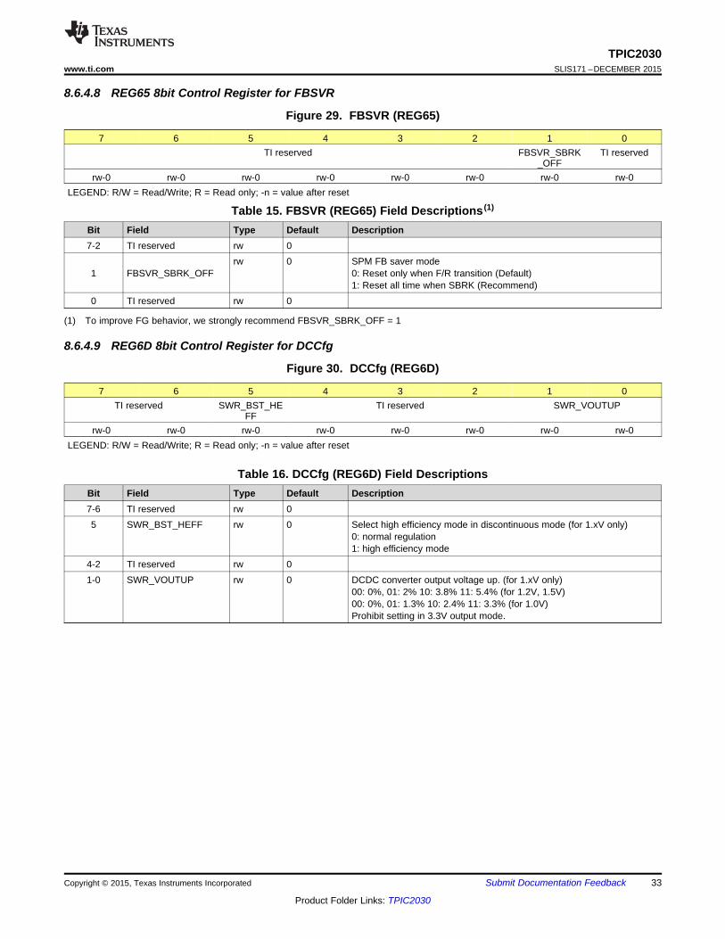
8.6.4.8 REG65 8bit Control Register for FBSVR
Figure 29. FBSVR (REG65)
7 6 5 4 3 2 1 0TI reserved FBSVR_SBRK
_OFFTI reserved
rw-0 rw-0 rw-0 rw-0 rw-0 rw-0 rw-0 rw-0LEGEND: R/W = Read/Write; R = Read only; -n = value after reset
(1) To improve FG behavior, we strongly recommend FBSVR_SBRK_OFF = 1
Table 15. FBSVR (REG65) Field Descriptions (1)
Bit Field Type Default Description7-2 TI reserved rw 0
1 FBSVR_SBRK_OFFrw 0 SPM FB saver mode
0: Reset only when F/R transition (Default)1: Reset all time when SBRK (Recommend)
0 TI reserved rw 0
8.6.4.9 REG6D 8bit Control Register for DCCfg
Figure 30. DCCfg (REG6D)
7 6 5 4 3 2 1 0TI reserved SWR_BST_HE
FFTI reserved SWR_VOUTUP
rw-0 rw-0 rw-0 rw-0 rw-0 rw-0 rw-0 rw-0LEGEND: R/W = Read/Write; R = Read only; -n = value after reset
Table 16. DCCfg (REG6D) Field DescriptionsBit Field Type Default Description7-6 TI reserved rw 05 SWR_BST_HEFF rw 0 Select high efficiency mode in discontinuous mode (for 1.xV only)
0: normal regulation1: high efficiency mode
4-2 TI reserved rw 01-0 SWR_VOUTUP rw 0 DCDC converter output voltage up. (for 1.xV only)
00: 0%, 01: 2% 10: 3.8% 11: 5.4% (for 1.2V, 1.5V)00: 0%, 01: 1.3% 10: 2.4% 11: 3.3% (for 1.0V)Prohibit setting in 3.3V output mode.

34
TPIC2030SLIS171 –DECEMBER 2015 www.ti.com
Product Folder Links: TPIC2030
Submit Documentation Feedback Copyright © 2015, Texas Instruments Incorporated
8.6.4.10 REG6E 8bit Control Register for UtilCfg
Figure 31. UtilCfg (REG6E)
7 6 5 4 3 2 1 0GPOUT_HL GPOUT_ENA TI reserved SWR_GPIO_C
NTLTI reserved
rw-0 rw-0 rw-0 rw-0 rw-0 rw-0 rw-0 rw-0LEGEND: R/W = Read/Write; R = Read only; -n = value after reset
Table 17. UtilCfg (REG6E) Field DescriptionsBit Field Type Default Description7 GPOUT_HL rw 0 GPOUT (General Purpose Output) pin output selection
0: low output1: high outputvalid only REG6F=00h
6 GPOUT_ENA rw 0 Enable monitor signal output to GPOUT pin0: No signal output, Hi-Z1: output signal selected in REG6F with CMOS outputOutput is Logical OR when selected two more signals
4 SWR_GPIO_CNTL rw 0 Set GPOUT output value (disable DCDC converter)0: output L in REGOUT pin (open drain)1: output H in REGOUT pin (open drain)
3-0 TI reserved rw 0
8.6.4.11 REG6F 8bit Control Register for MonitorSet (REG6F)
Figure 32. MonitorSet (REG6F)
7 6 5 4 3 2 1 0ACTTIMER_FL
T_MONENDDET_MON SIF_TIMEOUT
ERR_MONPWRERR_MO
NTSDERR_MON OCPERR_MO
NTSDFAULT_M
ONTI reserved
rw-0 rw-0 rw-0 rw-0 rw-0 rw-0 rw-0 rw-0LEGEND: R/W = Read/Write; R = Read only; -n = value after reset
Table 18. MonitorSet (REG6F) Field DescriptionsBit Field Type Default Description7 ACTTIMER_FLT_MON rw 0 Assign signal to GPIO pin
1: ACTTIMER fault output to GPOUT pin6 ENDDET_MON rw 0 Assign signal to GPIO pin
1: ENDDET monitor output to GPOUT pin5 SIF_TIMEOUTERR_MON rw 0 Assign signal to GPIO pin
1: SIF timeout monitor output to GPOUT pin4 PWRERR_MON rw 0 Assign signal to GPIO pin
1: PWRERR monitor output to GPOUT pin3 TSDERR_MON rw 0 Assign signal to GPIO pin
1: TSDERR fault output to GPOUT pin2 OCPERR_MON rw 0 Assign signal to GPIO pin
1: OCPERR fault output to GPOUT pin1 TSDFAULT_MON rw 0 Assign signal to GPIO pin
1: TSDFAULT fault output to GPOUT pin0 TI reserved rw 0

35
TPIC2030www.ti.com SLIS171 –DECEMBER 2015
Product Folder Links: TPIC2030
Submit Documentation FeedbackCopyright © 2015, Texas Instruments Incorporated
8.6.4.12 REG70 8bit Control Register for DriverEna
Figure 33. DriverEna (REG70)
7 6 5 4 3 2 1 0TLT_ENA FCS_ENA TRK_ENA SPM_ENA SLD_ENA SWR_MD_BUR
STLOAD_ENA XSLEEP
rw-0 rw-0 rw-0 rw-0 rw-0 rw-0 rw-0 rw-0LEGEND: R/W = Read/Write; R = Read only; -n = value after reset
Table 19. DriverEna (REG70) Field DescriptionsBit Field Type Default Description7 TLT_ENA rw 0 1 : Tilt enable (with XSLEEP=1)
It’s reset when XMUTE changes to L.6 FCS_ENA rw 0 1: Focus enable (with XSLEEP=1)
It’s reset when XMUTE changes to L.5 TRK_ENA rw 0 1: Track enable (with XSLEEP=1)
It’s reset when XMUTE changes to L.4 SPM_ENA rw 0 1: Spindle enable (with XSLEEP=1)
It’s reset when XMUTE changes to L.3 SLD_ENA rw 0 1: Sled enable (with XSLEEP=1)
It’s reset when XMUTE changes to L.2 SWR_MD_BURST rw 0 1 : Enable DCDC converter discontinuous regulation mode.
Regardless of the amount of current consumption, it will always be indiscontinuous mode. Holds a former value after XMUTE = L event.
1 LOAD_ENA rw 0 1 : LOAD enable (with XSLEEP=1)Track (bit5:TRK_ENA) will be disabled at LOAD_ENA=1 because ofsharing the DAC PWM module. Load priority is higher than TRK_ENA.It’s reset when XMUTE changes to L. (with LOAD_05CH=1)
0 XSLEEP rw 0 1: Operation mode 0 : Power save modeCharge pump enable bit.All driver enable bit (Bit[7:1]) change disabled and output change to Hi-Z(regardless of setting xxx_ENA bit is 1) when setting XSLEEP to 0.Therefore set 1 to XSLEEP before setting each enable bits.

36
TPIC2030SLIS171 –DECEMBER 2015 www.ti.com
Product Folder Links: TPIC2030
Submit Documentation Feedback Copyright © 2015, Texas Instruments Incorporated
8.6.4.13 REG71 8bit Control Register for FuncEna
Figure 34. FuncEna (REG71)
7 6 5 4 3 2 1 0SPM_LSMODE ENDDET_ENA SWR_BSTAUT
ONLED_ON CSW_ON TEMPMON_EN
ATI reserved
rw-0 rw-0 rw-0 rw-0 rw-0 rw-0 rw-0 rw-0LEGEND: R/W = Read/Write; R = Read only; -n = value after reset
Table 20. FuncEna (REG71) Field DescriptionsBit Field Type Default Description7 SPM_LSMODE rw 0 0 : Spindle rotation mode
1 : Light Scribe mode (slow rotation mode)6 ENDDET_ENA rw 0 1 : use Sled end detection enable ( with SLD_ENA=1)5 SWR_BSTAUTON rw 0 1 : Enable auto DCDC converter discontinuous regulation mode.
At low current consumption, it changes to discontinuous modeautomatically. Holds a former value after XMUTE = L event.SWR_BSTAUTON mode is chosen when both bit SWR_BSTAUTONand SWR_MD_BURST are set.
4 LED_ON rw 0 1 : LEDO enable ( with XSLEEP=1)3 CSW_ON rw 0 1 : CSWO enable ( with XSLEEP=1)
It’s reset when XMUTE changes to L2 TEMPMON_ENA rw 0 1: enable chip temperature monitoring ( with XSLEEP=1)
1-0 TI reserved rw 0
8.6.4.14 REG72 8bit Control Register for ACTCfg
Figure 35. ACTCfg (REG72)
7 6 5 4 3 2 1 0LOAD_O5CH_
HIGHLOADPROT_O
FFACTPROT_OF
FACTTEMPTH
rw-0 rw-0 rw-0 rw-0 rw-0 rw-0 rw-0 rw-0LEGEND: R/W = Read/Write; R = Read only; -n = value after reset
Table 21. ACTCfg (REG72) Field DescriptionsBit Field Type Default Description7 LOAD_05CH_HIGH rw 0 LOAD output polarity at 0.5CH ( REG74h[6]=1 )
0: LOADP=Low1: LOADP=High
6 LOADPROT_OFF rw 0 1: Load Overcurrent Protection OFF5 ACTPROT_OFF rw 0 0 : Actuator protection ON 1 : Actuator Fault monitor disable (No
protection for ACT channel)4-0 ACTTEMPTH rw 0 Actuator thermal protection (=ACT Timer) threshold level
ACT Timer Protection enable except ACTTEMPTH[4:0]=0x00ACTTEMPTH = 0x00 equal to ACTPROT_OFF = 1By writing value 0x00, ACTTIMER_PROT flag is cleared.
37
TPIC2030www.ti.com SLIS171 –DECEMBER 2015
Product Folder Links: TPIC2030
Submit Documentation FeedbackCopyright © 2015, Texas Instruments Incorporated
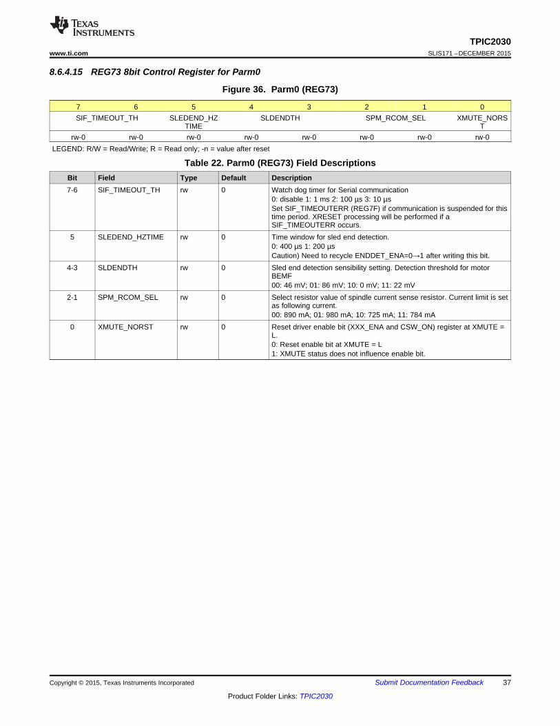
8.6.4.15 REG73 8bit Control Register for Parm0
Figure 36. Parm0 (REG73)
7 6 5 4 3 2 1 0SIF_TIMEOUT_TH SLEDEND_HZ
TIMESLDENDTH SPM_RCOM_SEL XMUTE_NORS
Trw-0 rw-0 rw-0 rw-0 rw-0 rw-0 rw-0 rw-0
LEGEND: R/W = Read/Write; R = Read only; -n = value after reset
Table 22. Parm0 (REG73) Field DescriptionsBit Field Type Default Description7-6 SIF_TIMEOUT_TH rw 0 Watch dog timer for Serial communication
0: disable 1: 1 ms 2: 100 µs 3: 10 µsSet SIF_TIMEOUTERR (REG7F) if communication is suspended for thistime period. XRESET processing will be performed if aSIF_TIMEOUTERR occurs.
5 SLEDEND_HZTIME rw 0 Time window for sled end detection.0: 400 µs 1: 200 µsCaution) Need to recycle ENDDET_ENA=0→1 after writing this bit.
4-3 SLDENDTH rw 0 Sled end detection sensibility setting. Detection threshold for motorBEMF00: 46 mV; 01: 86 mV; 10: 0 mV; 11: 22 mV
2-1 SPM_RCOM_SEL rw 0 Select resistor value of spindle current sense resistor. Current limit is setas following current.00: 890 mA; 01: 980 mA; 10: 725 mA; 11: 784 mA
0 XMUTE_NORST rw 0 Reset driver enable bit (XXX_ENA and CSW_ON) register at XMUTE =L.0: Reset enable bit at XMUTE = L1: XMUTE status does not influence enable bit.

38
TPIC2030SLIS171 –DECEMBER 2015 www.ti.com
Product Folder Links: TPIC2030
Submit Documentation Feedback Copyright © 2015, Texas Instruments Incorporated
8.6.4.16 REG74 8bit Control Register for OptSet
Figure 37. OptSet (REG74)
7 6 5 4 3 2 1 0DIFF_TLT LOAD_05CH RDSTAT_ON_
VFCSVSLD2_POL LOAD_OCP_
IUPTI reserved SOMI_HIZ VDAC_MAPSW
rw-0 rw-0 rw-0 rw-0 rw-0 rw-0 rw-0 rw-0LEGEND: R/W = Read/Write; R = Read only; -n = value after reset
Table 23. OptSet (REG74) Field DescriptionsBit Field Type Default Description7 DIFF_TLT rw 0 1 : Differential Tilt mode enable (with TLT_ENA=FCS_ENA=1)
Differential Tilt mode (DIFF_TLT=1), DAC value setting as followsFCS_OUT = (VFCS + VTLT) × 6 / 2048TLT_OUT = (VFCS – VTLT) × 6 / 2048In DIFF_TLT mode (DIFF_TLT = 1), TLT_OUT should be changed afterwriting VFCS.
6 LOAD_05CH rw 0 The setting of Load motor driving type. Load output changes as follow0: step down mode (LOAD output is controlled by DAC code, VLOAD)Use for Slot-in model or step down tray model.1: 0.5Ch mode (LOAD is only controlled by LOAD_05CH_HIGH)Use for Tray model
5 RDSTAT_ON_VFCS rw 0 Set Read status data (REG7F) at VFCS write command (REG02)1: enable Write and Read mode(Write 12-bits Focus DAC data + Read 8bits status data)
4 VSLD2_POL rw 0 change direction of SLED rotation3 LOAD_OCP_IUP rw 0 Select over current protection (OCP) threshold for Load channel current
0: 250mA1: 425mA
2 TI reserved rw 01 SOMI_HIZ rw 0 0: SOMI line High-Z at bus idling time.
1: SOMI line Pull Down at bus idling time.0 VDAC_MAPSW rw 0 Selection of DAC register channel assignments (REG01~09)
8.6.4.17 REG76 8bit Control Register for WriteEna
Figure 38. WriteEna (REG76)
7 6 5 4 3 2 1 0WRITE_ENABLE TI reserved
rw-0 rw-0 rw-0 rw-0 rw-0 rw-0 rw-0 rw-0LEGEND: R/W = Read/Write; R = Read only; -n = value after reset
Table 24. WriteEna (REG76) Field DescriptionsBit Field Type Default Description7 WRITE_ENABLE 0 0: Register Write disable except REG76
1: Write enable for registers REG01~0B, REG70~7F, REG6C~6F6-0 TI reserved

39
TPIC2030www.ti.com SLIS171 –DECEMBER 2015
Product Folder Links: TPIC2030
Submit Documentation FeedbackCopyright © 2015, Texas Instruments Incorporated
8.6.4.18 REG77 8bit Control Register for ClrReg
Figure 39. ClrReg (REG77)
7 6 5 4 3 2 1 0RST_INDAC RST_REGS RST_ERR_FLAG RST_REGS_WO3 TI reserved
w-0 w-0 w-0 w-0 w-0 w-0 w-0 w-0LEGEND: R/W = Read/Write; R = Read only; -n = value after reset
Table 25. ClrReg (REG77) Field DescriptionsBit Field Type Default Description7 RST_INDAC w 0 1 : Reset all 12-bit input DAC register (REG01~0B)
*Self clear bit6 RST_REGS w 0 1 : Reset all 8bit R/W Registers (REG70h~77h, 60h-6Fh)
*Self clear bit5 RST_ERR_FLAG w 0 1 : Reset Fault Flag Latch (REG7F[5:1], REG79~REG7B)
*Self clear bit4-0 TI reserved w 0
8.6.4.19 REG78 8bit Control Register for ActTemp
Figure 40. ActTemp (REG78)
7 6 5 4 3 2 1 0TI reserved ACT_TIMER_
PROTACTTEMP
r-0 r-0 r-0 r-0 r-0 r-0 r-0 r-0LEGEND: R/W = Read/Write; R = Read only; -n = value after reset
Table 26. ActTemp (REG78) Field DescriptionsBit Field Type Default Description7-6 TI reserved r 05 ACT_TIMER_PROT r 0 ACT timer protection flag
1: ACT Timer Protection has detected and latched.(ACTTEMP > ACTTEMPTH)This bit holds data after temperature change to low since this is a latchbit. Also driver output keep Hi-Z until setting RST_ERR_FLAG orACTTEMPTH=0.
4-0 ACTTEMP r 0 An integrated value of ACT_TIMER counters at present.

40
TPIC2030SLIS171 –DECEMBER 2015 www.ti.com
Product Folder Links: TPIC2030
Submit Documentation Feedback Copyright © 2015, Texas Instruments Incorporated
8.6.4.20 REG79 8bit Control Register for UVLOMon
Figure 41. UVLOMon (REG79)
7 6 5 4 3 2 1 0TI reserved XMUTE_
DETECTUVLO_P5V UVLO_INT3P3 UVLO_SIOV UVLO_SWR OVP_P5V
r-0 r-0 r-0 r-0 r-0 r-0 r-0 r-0LEGEND: R/W = Read/Write; R = Read only; -n = value after reset
(1) Latched first event only. Cleared by RST_ERR_FLG (REG77)
Table 27. UVLOMon (REG79) Field DescriptionsBit Field Type Default Description7-6 TI reserved r 05 XMUTE_DETECT r 0 XMUTE flag for detection Lo input. (>20 µs) (1)
4 UVLO_P5V r 0 UVLO (Under Voltage Lock Out) flag for detection Low P5V supply (1)
3 UVLO_INT3P3 r 0 UVLO flag for detection Low internal 3.3-V regulator (1)
2 UVLO_SIOV r 0 UVLO flag for detection Low SIOV (1)
1 UVLO_SWR r 0 UVLO flag for detection Low DCDC (1)
0 OVP_P5V r 0 Over voltage protection flag for P5Vsply (1)
8.6.4.21 REG7A 8bit Control Register for TsdMon
Figure 42. TsdMon (REG7A)
7 6 5 4 3 2 1 0TSD_FAULT_S
WRTSD_FAULT_S
PMTSD_FAULT_A
CTTSD_FAULT_L
EDCSWTSD_SWR TSD_SPM TSD_ACT TSD_
LEDCSWr-0 r-0 r-0 r-0 r-0 r-0 r-0 r-0
LEGEND: R/W = Read/Write; R = Read only; -n = value after reset
(1) Cleared by RST_ERR_FLAG bit (REG77)
Table 28. TsdMon (REG7A) Field DescriptionsBit Field Type Default Description7 TSD_FAULT_SWR r 0 Pre alert of thermal protection for DCDC converter block (1)
6 TSD_FAULT_SPM r 0 Pre alert of thermal protection of Spindle block (1)
5 TSD_FAULT_ACT r 0 Pre alert of thermal protection of Focus /Track /Tilt Sled1 /Sled2 //Load (1)
4 TSD_FAULT_LEDCSW
r 0 Pre alert of thermal protection of CSW/LED (1)
3 TSD_SWR r 0 Thermal protection flag for DCDC converter block (1)
DCDC converter output Hi-Z until temperature falls on release level1: detect (latch)
2 TSD_SPM r 0 Thermal protection flag for Spindle (1)
SPM output Hi-Z until temperature falls on release level1: detect (latch)
1 TSD_ACT r 0 Thermal protection flag for Focus /Track /Tilt Sled1 /Sled2 /Load (1)
Actuator output Hi-Z until temperature falls on release level1: detect (latch)
0 TSD_ LEDCSW r 0 Thermal protection flag for CSW/LED (1)
LED/CSW output Hi-Z until temperature falls on release level1: detect (latch)
41
TPIC2030www.ti.com SLIS171 –DECEMBER 2015
Product Folder Links: TPIC2030
Submit Documentation FeedbackCopyright © 2015, Texas Instruments Incorporated
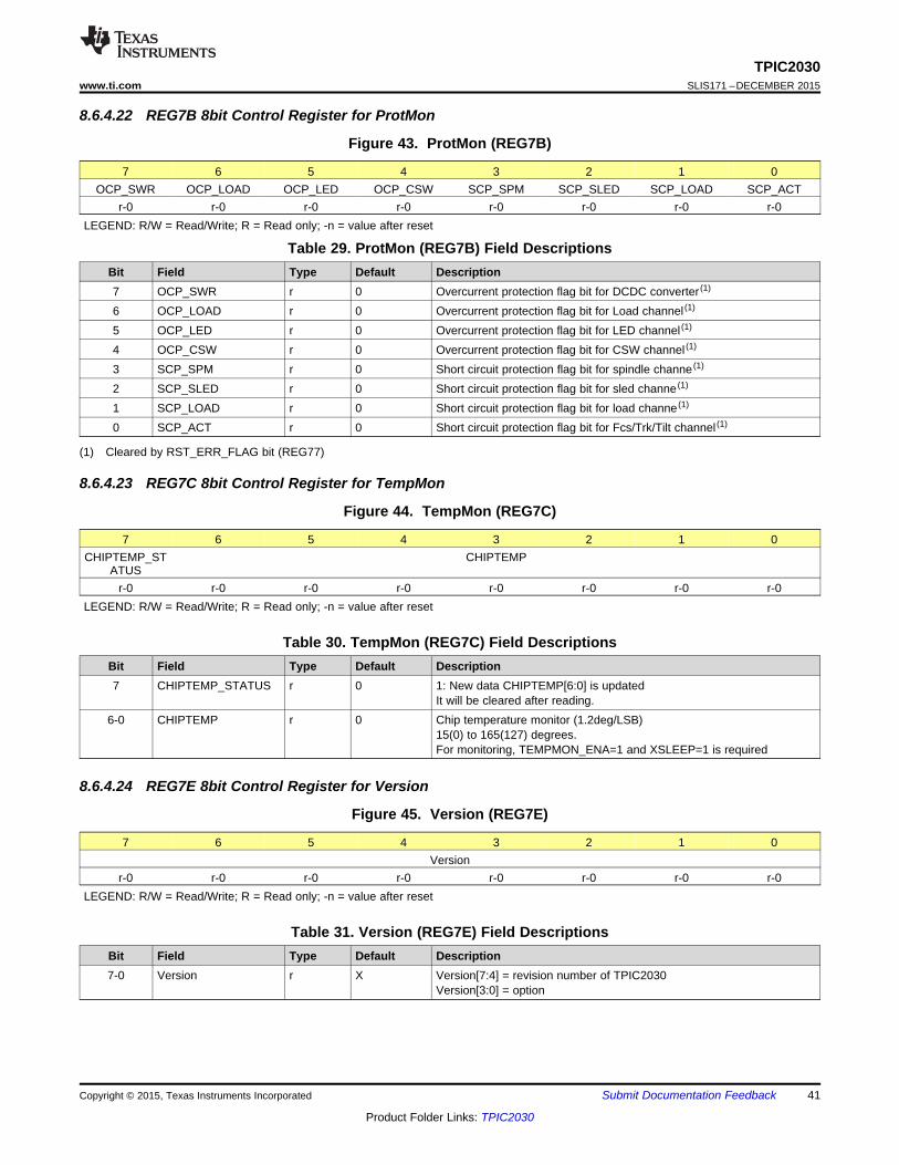
8.6.4.22 REG7B 8bit Control Register for ProtMon
Figure 43. ProtMon (REG7B)
7 6 5 4 3 2 1 0OCP_SWR OCP_LOAD OCP_LED OCP_CSW SCP_SPM SCP_SLED SCP_LOAD SCP_ACT
r-0 r-0 r-0 r-0 r-0 r-0 r-0 r-0LEGEND: R/W = Read/Write; R = Read only; -n = value after reset
(1) Cleared by RST_ERR_FLAG bit (REG77)
Table 29. ProtMon (REG7B) Field DescriptionsBit Field Type Default Description7 OCP_SWR r 0 Overcurrent protection flag bit for DCDC converter (1)
6 OCP_LOAD r 0 Overcurrent protection flag bit for Load channel (1)
5 OCP_LED r 0 Overcurrent protection flag bit for LED channel (1)
4 OCP_CSW r 0 Overcurrent protection flag bit for CSW channel (1)
3 SCP_SPM r 0 Short circuit protection flag bit for spindle channe (1)
2 SCP_SLED r 0 Short circuit protection flag bit for sled channe (1)
1 SCP_LOAD r 0 Short circuit protection flag bit for load channe (1)
0 SCP_ACT r 0 Short circuit protection flag bit for Fcs/Trk/Tilt channel (1)
8.6.4.23 REG7C 8bit Control Register for TempMon
Figure 44. TempMon (REG7C)
7 6 5 4 3 2 1 0CHIPTEMP_ST
ATUSCHIPTEMP
r-0 r-0 r-0 r-0 r-0 r-0 r-0 r-0LEGEND: R/W = Read/Write; R = Read only; -n = value after reset
Table 30. TempMon (REG7C) Field DescriptionsBit Field Type Default Description7 CHIPTEMP_STATUS r 0 1: New data CHIPTEMP[6:0] is updated
It will be cleared after reading.6-0 CHIPTEMP r 0 Chip temperature monitor (1.2deg/LSB)
15(0) to 165(127) degrees.For monitoring, TEMPMON_ENA=1 and XSLEEP=1 is required
8.6.4.24 REG7E 8bit Control Register for Version
Figure 45. Version (REG7E)
7 6 5 4 3 2 1 0Version
r-0 r-0 r-0 r-0 r-0 r-0 r-0 r-0LEGEND: R/W = Read/Write; R = Read only; -n = value after reset
Table 31. Version (REG7E) Field DescriptionsBit Field Type Default Description7-0 Version r X Version[7:4] = revision number of TPIC2030
Version[3:0] = option

42
TPIC2030SLIS171 –DECEMBER 2015 www.ti.com
Product Folder Links: TPIC2030
Submit Documentation Feedback Copyright © 2015, Texas Instruments Incorporated
8.6.4.25 REG7F 8bit Control Register for Status
Figure 46. Status (REG7F)
7 6 5 4 3 2 1 0ACTTIMER_FA
ULTENDDET SIF_TIMEOUT
ERRPWRERR TSDERR OCPERR TSDFAULT FG
r-0 r-0 r-0 r-0 r-0 r-0 r-0 r-0LEGEND: R/W = Read/Write; R = Read only; -n = value after reset
Table 32. Status (REG7F) Field DescriptionsBit Field Type Default Description7 ACTTIMER_FAULT r 0 Status flag of ACTTIMER protection
1: Pre alert of ACTTIMER protection. It is close to the threshold level.You can get current ACTTIMER value in REG78.Both of this bit and ACT_TIMER_PROT (REG78) will be set when overthe threshold.
6 ENDDET r 0 status flag of END detection1: end position detected (not latch bit)
5 SIF_TIMEOUTERR r 0 error flag of serial I/F watch dog timer1: SIF communication was interrupted, expired watch dog timer
4 PWRERR r 0 error flag of Power1 : Voltage problem occurred, details in REG79
3 TSDERR r 0 error flag of any over thermal protections1: Dispatched thermal protection, details in REG7A
2 OCPERR r 0 error flag of any over current protection1: Dispatched OCP, details in REG7Bh
1 TSDFAULT r 0 warning of TSD of any thermal protection1 : Detect pre thermal protection details in REG7A
0 FG r 0 FG signal. Spindle rotation pulse for speed monitor

43
TPIC2030www.ti.com SLIS171 –DECEMBER 2015
Product Folder Links: TPIC2030
Submit Documentation FeedbackCopyright © 2015, Texas Instruments Incorporated
9 Application and Implementation
NOTEInformation in the following applications sections is not part of the TI componentspecification, and TI does not warrant its accuracy or completeness. TI’s customers areresponsible for determining suitability of components for their purposes. Customers shouldvalidate and test their design implementation to confirm system functionality.
NOTE• Operate every driver channel after 5-V power supplied and stable.• Appropriate capacity of de-coupling capacitor is required enough value of over 10μF
due to reduce influence of PWM switching noise. And the P5V pin needs to connect afilter of 1μF. It is effective to put bypass capacitor(about 0.1uF) near Powerpin(P5V_1,P5V_2, P5V_SW,P5V_SPM)for PWM switching noise reduction onpower and GND line.
• Much current flow to driver circuits, to consider as below matters.– Pattern-lay-out and line-impedance. And noise influence from supply line.
9.1 Application Information
9.1.1 DAC TypeTPIC2030 has nine channels of Actuator. Each channel is assigned to the most suitable DAC engine with adifferent type respectively. ACT(F/T/Ti) has 12-bit DAC. Upper 8 (MSB sign bit) are converted at a time in 5 MHzand LSB 4 bits are output in sequence with 1.25-MHz PWM. SPIN, SLED, and Load DAC has same DAC typesand sampling rate with 312 kHz. All channels except SLED have x6 gain. Table 33 shows configuration of eachactuator.
Table 33. DAC TypeFCS/TRK/TLT SLED SPIN LOAD
Resolution 12 bit 10 bit 12 bit 12 bitType 8-bit oversampling 10-bit voltage 8-bit oversampling 8-bit oversampling
Sampling 1.25M / 10bit312K / 12bit 312K 312K
PWM frequency 312 kHz About 156 kHz(variable) 156 kHz 312 kHzOut range ±6 V ±440 mA ±6 V ±6 V
Feedback Voltage feedback Current feedback Power supplycompensation
Voltage feedbackShared with TRK
9.1.2 Example Sampling Rate of 12-Bit DAC for FCS/TRK/TLTThe input data is separated in the upper 8 bits and the lower 4 bits. Upper 8 bits (MSB sign 1 bit) will be put into8bit current DAC in every 5 MHz. The lower 4bits will be put into one bit current DAC in sequence from upper tolower bit. This one-bit DAC output with PWM in 1.25 MHz. At any PWM duty, 100%, 75%, 50%, 25%, or 0%, willbe summed in 8-bit current DAC in every 1.25 MHz. Thus, it takes 3.2 µs for all lower 4bits summing to PWMoutput. As a result, 12 bit data is sampled in every PWM cycle. Example of sampling rate for FCS/TRK/TLT isFigure 47.

1 2 3 1 1
1 2 3 1 1 1 2
V d a c 1 .0 b it [1 0 ] 0 .5 b it [9 ] 0 .5 b it [8 ] 0 .5 .. . b i t [0 ] 0 .5
9 G D F ± E LW > @ E LW > @ E LW > @ . b it [0 ] 0 .5 0 .5
V o u t V d a c 6 .0 ( V )
S L E D Io u t V d a c 0 .4 4 ( A )
u u u u u
u u u u u
u
u
6 .0V o u t D A C c o d e
2 0 4 8 u
8 8 8 8 8 8 8 8 8 8 8 8 8 8 8 8 8 8
10 bit 10 bit 10 bit 10 bit
11 bit 11 bit
12 bit
White DAC
625 kHz
1.25 MHz
5 MHz
312 kHz
PWM duty
LSB 4-bit width
12-bit DAC (8-bit DAC + 4-bit PWM DAC) output
one PWM cycle (312 kHz = 3.2 s)µ
44
TPIC2030SLIS171 –DECEMBER 2015 www.ti.com
Product Folder Links: TPIC2030
Submit Documentation Feedback Copyright © 2015, Texas Instruments Incorporated
Figure 47. Example of 12-Bit DAC Conversion Time (FCS/TRK/TLT)
9.1.3 Digital Input CodingThe output voltage (current) is commanded via programming to the DAC. All of the DAC input format is 12bit in2’s complement though some DAC has a low resolution. When 12 bits data is input 8 bits DAC, TPIC2030recognizes four subordinate position bits (LSB) as 0. To arrange for 12-bit DAC format, DSP should shift 8bit or10 bit data to an appropriate bit position. The full scale is ±1.0 V and driver gain is set 6. The output voltage(Vout) is given by the following equation:
(1)
where• bit[11:0] is the digital input value, range 000000000000b to 111111111111b. (2)
Table 34. DAC FormatMSB DIGITAL INPUT (BIN) LSB HEX DEC VDAC ANALOG OUTPUT
1000_0000_0000 0x800 –2048 –0.9995 –5.9971000_0000_0001 0x801 –2047 –0.9995 –5.9971111_1111_1111 0xFFF –1 –0.0005 –0.0030000_0000_0000 0x000 0 0 0.0000000_0000_0001 0x001 +1 +0.0005 +0.0030111_1111_1110 0x7FE +2046 +0.9990 +5.9940111_1111_1111 0x7FF +2047 +0.9995 +5.997

DAC code7FFh000800h
+ 6.0
–6.0
VDAC
+ 1.000
–1.000
+ 5.0
–5.0
*
*
Analog output (V)
* following P5V input voltage
45
TPIC2030www.ti.com SLIS171 –DECEMBER 2015
Product Folder Links: TPIC2030
Submit Documentation FeedbackCopyright © 2015, Texas Instruments Incorporated
Figure 48. Output Voltage vs DAC Code
9.1.4 Example Timing of Target Control SystemTPIC2030 is designed for that meets the requirements updating control data in 400 kHz. The example of controlsystem parameter is listed in . It takes 0.51 µs for transmit a 16-bit data packet to TPIC2030 with 35 MHz SCLK.Therefore, DSP can be sent four packets a 400-kHz interval. If SCLK is lower than 28.8 MHz, it is requiredreducing packet quantity under three. For example, Focus/Track command is updating in every 2.5 µs (400 kHz),and it is able to send another two kind of packet in this same slot. shows the example of the control timing whenTPIC2030 is used.
Table 35. Example Timing of Target Control SystemSIGNAL BIT UPDATE CYCLE (kHz)Focus 12 400Track 12 400
Tilt 12 200Sled1 10 100Sled2 10 100
Spindle 12 100Load 12 —

VSPM[11.0] < 0VSPM[11.0] > 0 0
> 15 ms
300 ms
time130 rpm
speed
XRESET
WRITE_ENABLE
XSLEEP
SPM_ENA
VSPM
XFG
brake
Release
Focus
Track
Tilt
Sled1
Sled2
SPM
Load
Control
reg ister
312 kHz /3.2 µs (PWM one cycle)
400 kHz /2.5 µs
100 kHz /10 µs (one control cycle)
RRRRR
DAC command
DAC command with status read
Control register command
PWM cycle
0.51 µs (SCLK:35 MHz) for data transmitR
46
TPIC2030SLIS171 –DECEMBER 2015 www.ti.com
Product Folder Links: TPIC2030
Submit Documentation Feedback Copyright © 2015, Texas Instruments Incorporated
Figure 49. Example DAC Control
9.1.5 Spindle Motor Driver PartWhen VSPM is set to a positive DAC code then the part will be in acceleration mode. IS mode operates then thestart-up circuit offers the special start-up pattern sequence to the driver in start-up, and then switches to spin-upmode by detecting the rotor position by BEMF signal from the spindle motor coil.
The spin-down and brake function also be controlled by VSPM DAC value. When it is set the brake command toVSPM, driver goes into active-brake mode, then switch to short-brake mode in slow revolution speed, and thenstop automatically. The FG signal is composed from EXOR of three-phase signal, and is output from XFG pinshown in Figure 50.
Figure 50. Spindle Operating Sequence
• It is recommended to use down-edge of FG signal for monitoring FG frequency. The FG terminal needs to bepull up to the appropriate supply voltage by external resistor.
• Short Brake mode is asserted after 300 ms of FG signal stays L-level in deceleration.• The FG output is set to H-level in sleep mode in order to reduce sleep mode current.• This value is the nominal number of using motor with 16-poles.

Active
Active
Slow down
3-phaseshort
2-p
hase s
hort
4000
3000
2000
1000
0
800h A00h FAEh000
VSPM[11:0]
rpm
PWM Output Duty
SPM_LSMODE = 0
100%
0%
800h FAEh 000 52h 7FFh
VSPM[11:0]
Speed UpSlow Down
Dead BandDuty = 0%
Output (V)
25%
6.0 V
5.0 V
47
TPIC2030www.ti.com SLIS171 –DECEMBER 2015
Product Folder Links: TPIC2030
Submit Documentation FeedbackCopyright © 2015, Texas Instruments Incorporated
• First of all, power supply voltage of P5V must be supplied before any signals input.
9.1.5.1 Spindle PWM ControlThe output PWM duty of Spindle is controlled by DAC code (VSPM). The gain in acceleration setting is alwayssix times. However, the maximum output is restricted to P5V_SPM voltage. A dead band which output = 0 existsin the width of plus or minus 0x52 focusing on zero.
Figure 51. Spindle PWM Control
9.1.5.2 Auto Short Brake FunctionTPIC2030 provides auto short brake function which is selecting brake mode automatically by motor speed.
Auto Short Brake is the intelligent brake function that includes 2 modes, Short Brake and Active Brake.
When VSPM value is controlled more than equivalent 75% duty brake, deceleration is done by short brake underthe rotation speed is over 3000 rpm. After deceleration, driver goes into Active-brake mode automatically byinternal logic circuit under rotation speed is lower 2000 rpm. This function enables low power consumption andsilent during braking.
Table 36. Brake Mode
VSPM[11:0]ROTATION SPEED((RPM)
ABOUT 0 TO 2000 ABOUT 30000x000 - 0xFAE 2-phase short Brake 2-phase short Brake0xFAE - 0xA00 Active Brake Active Brake0xA00 - 0x800 Active Brake 3-phase short Brake
Figure 52. Brake Mode Selections
This value is the nominal number of using motor with 16-poles motor.

Speed upDuty = 0%
6.0 V
5.0 V
PWM Output Duty
100%
25%
0% VSPM[11:0]
Output (V)
SPM_LSMODE = 1
800h 000 7FFh
48
TPIC2030SLIS171 –DECEMBER 2015 www.ti.com
Product Folder Links: TPIC2030
Submit Documentation Feedback Copyright © 2015, Texas Instruments Incorporated
9.1.5.3 Spindle Low Speed ModeLS mode is the low rotation mode which made the maximum 25% duty. When using SPM_LSMODE = 1, brakemode is always SHORT BRAKE. shows the output duty of LS mode.
Figure 53. Spindle PWM Control (Low Speed Mode)
9.1.5.4 Spindle Driver Current Limit CircuitThis IC builds in the SPM current sense resistor which can select resistor value. .
The spindle current limit circuit monitors motor current which flows through this resistance, and limits the outputcurrent by reducing PWM duty when detecting over current conditions. shows resistor value.
A limit current value can be calculated from following formulas.
Limit current = 196mV / resistor value
Table 37. SPM Current Sense ResistorSPM_RCOM_SEL[1:0] RESISTOR VALUE (Ω) LIMIT CURRENT (mA)
00 0.22 89001 0.20 98010 0.27 72511 0.25 784
9.1.6 Sled Driver Part
9.1.6.1 Sled Channel Input vs Output PWM DutyThe Sled driver outputs the PWM pulse set as DAC code (VSLDx) with current feed back. The maximum outputis restricted to 440mA at 0x7FF and 0x800. A dead band which output = 0 exists in the width of plus or minusfocusing on zero.
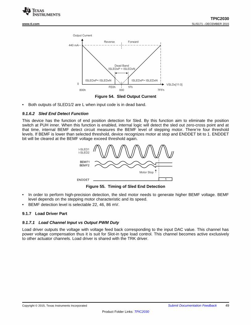
ENDDET
BEMF1
BEMF2
1
Motor Stop
I-SLED1I-SLED2
Output Current
Reverse Forward
440 mA
0
800hFE0h
0001Fh
7FFh
VSLDx[11:0]
ISLEDxP> ISLEDxNISLEDxP< ISLEDxN
Dead BandISLEDxP = ISLEDxN
49
TPIC2030www.ti.com SLIS171 –DECEMBER 2015
Product Folder Links: TPIC2030
Submit Documentation FeedbackCopyright © 2015, Texas Instruments Incorporated
Figure 54. Sled Output Current
• Both outputs of SLED1/2 are L when input code is in dead band.
9.1.6.2 Sled End Detect FunctionThis device has the function of end position detection for Sled. By this function aim to eliminate the positionswitch at PUH inner. When this function is enabled, internal logic will detect the sled out zero-cross point and atthat time, internal BEMF detect circuit measures the BEMF level of stepping motor. There’re four thresholdlevels. If BEMF is lower than selected threshold, device recognizes motor at stop and ENDDET bit to 1. ENDDETbit will be cleared at the BEMF voltage exceed threshold again.
Figure 55. Timing of Sled End Detection
• In order to perform high-precision detection, the sled motor needs to generate higher BEMF voltage. BEMFlevel depends on the stepping motor characteristic and its speed.
• BEMF detection level is selectable 22, 46, 86 mV.
9.1.7 Load Driver Part
9.1.7.1 Load Channel Input vs Output PWM DutyLoad driver outputs the voltage with voltage feed back corresponding to the input DAC value. This channel haspower voltage compensation thus it is suit for Slot-in type load control. This channel becomes active exclusivelyto other actuator channels. Load driver is shared with the TRK driver.

000 7FFh800h
ACT(FCS/TRK/TLT)[11:0]
forw ardreverse
100%
0%
PW M output duty
P5V
ACT+ > ACT-ACT+ < ACT-
PWM Output Duty Output (V)
6.0 V
5.0 V
VLOAD[11:0]
7FFhFE0h 000 1Fh800h
0%
100%
Load+ > Load–Load+ < Load–
Dead BandDuty = 0%
50
TPIC2030SLIS171 –DECEMBER 2015 www.ti.com
Product Folder Links: TPIC2030
Submit Documentation Feedback Copyright © 2015, Texas Instruments Incorporated
Figure 56. Load Output Duty
• Output voltage is controlled by PWM• Both LOAD+ and LOAD- are connected to PGND through the internal clamp diode respectively.
9.1.8 Focus/Track/Tilt Driver Part
Figure 57. FCS/TRK/TLT Output Duty
9.1.8.1 Differential Tilt ModeTPIC2030 support differential Tilt mode which output the value calculated from Focus and Tilt. Focus and Tilt canbe set in differential mode by DIFF_TLT (REG74) = 1. Because Focus and Tilt are updated at the same time, theupdate interval of Tilt can be thinned out. Output data changes at after writing VFCS data. Therefore it isnecessary to write VFCS data when set VTLT. In differential mode, the output value is calculated as follows.
9.1.9 Step-Down Synchronous DC-DC ConverterTPIC2030 has a synchronous step-down DC-DC converter which can output various voltages. Switchingfrequency is 2.5MHz. Because the ripple current in the coil can reduce, the smaller inductor value can beselected. And the inductor with lowest DC resistance can be selected for highest efficiency. And the regulatorshave fast transient response.

CLK2.5 MHz
SWR_MD_BURST
REGFB
REGOUT
REGOUTOutput Hi-Z term
REGOUTOutput Hi-Z
Discontinuous Mode
•• ••
•• ••
•• ••
•• ••
51
TPIC2030www.ti.com SLIS171 –DECEMBER 2015
Product Folder Links: TPIC2030
Submit Documentation FeedbackCopyright © 2015, Texas Instruments Incorporated
(1) It is necessary to maintain REGFB > 3.7 V for 100 µs in DC-DC working.
Step-down DC-DC converter produces an output 1.0, 1.2, 1.5, and 3.3 V. It only requires an external inductorand bypass capacitor(s). The gate drivers and compensations are all internal to the chip. The required inputsupply is 5 V for P5V_SW. It has a soft start approximately about 0.8 ms to limit the in-rush current when theregulator comes alive. The soft-start circuit uses the internal clock to profile its ramp.
It’s able to up 2%, 3.8% and 5.4% of the output voltage by setting SWR_VOUTUP (REG6D) for 1.2 V and 1.5 V,up 1.3%, 2.4%, and 3.3% for 1.0V.
Table 38. Output Voltage SettingSWR_VSEL2 SWR_VSEL1 INPUT REGFB DCDC CONVERTER OUTPUT
0 0 <3.7 V 3.3 V0 1 <3.7 V 1.2 V1 0 <3.7 V 1.0 V1 1 <3.7 V 1.5 VX X over 3.7V Disable (1)
9.1.9.1 Discontinuous Regulation ModeProvide a regulation mode named discontinuous regulation mode, which improves the conversion efficiency at alow current loading by changing regulation timing. Discontinuous mode is able to set 1 to SWR_MD_BURST(REG6D) bit. Furthermore by setting SWR_BSTAUTON (REG6D), the discontinuous mode is automaticallychosen at the time of low power consumption. shows the discontinuous regulation action. The currentconsumption has been reduced by shortening the energizing time of driving FET. On the other hand, DC voltageripple grows.
Figure 58. Discontinuous Regulation Mode
9.1.9.2 High Efficiency Mode (in Discontinuous Regulation Mode)The high efficiency mode which raises efficiency further at the time of low consumption can be chosen for 1.0 V,1.2 V, and 1.5 V. This mode is selected by SWR_BST_HEFF = 1 (REG6D) in discontinuous mode.
9.1.10 Monitor Signal on GPOUTThe device can output a specific signal to the GPOUT pin. To output a signal, choose a signal from REG6F byenabling first, then enable GPOUT_ENA. When two or more signals are set for GPOUT, the output is a logicalsum.

1 44
2 43
3 42
4 41
5 40
6 39
7 38
8 37
9 36
10 35
11 34
12 33
13 32
14 31
15 30
16 29
17 28
18 27
19 26
20 25
21 24
22 23
PGND_1
PGND_SW
REGOUT
LOAD+
SLED2-
SLED2+P5V_SW
REGFB
SIOV
TRK-
SLED1+
SWR_VSEL1
SSZ
SCLK
CSWOSWR_VSEL2
SOMI
MCOM
XMUTE
P5V_1
XFG
P5V_SPM
XRESET
W
GPOUT
CP1
V
CP2
GND_SPM
CP3 FCS+
SIMO
TLT-
TRK+
FCS-
PGND_2
TLT+
P5V_2
U
AGND
CV3P3
LEDO
SLED1-
LOAD-TPIC2030
U
V
W
MCOM
SOMI
SSZ
SCLK
SIMO
GPOUT
3.3V
XMUTE
XRESET
XFG
0.1 µF
P5V
0.1 µF
0.1 µF
10 µF 0.1 µF
1.x/3.3Voutput
10 µF
LEDO
CSWO
0.1 µF
0.1 µF10 µF
10 µF
10 µF
2.2 µH
52
TPIC2030SLIS171 –DECEMBER 2015 www.ti.com
Product Folder Links: TPIC2030
Submit Documentation Feedback Copyright © 2015, Texas Instruments Incorporated
9.2 Typical Application
Figure 59. Example of Application Circuit
Table 39. Pin Connection When Specific Function isnot Applied
FUNCTION PIN NUMBER CONNECTION
DC-DCconverter
SWR_VSEL1 7 GNDSWR_VSEL2 8 GND
P5V_SW 4 P5VPGND_SW 2 GNDREGOUT 3 OpenREGFB 5 P5V
9.2.1 Design RequirementsTo begin the design process, determine the following:1. Motor configuration: The user can use all motor channels or some of them.2. Power up devices with a 5-V supply.
9.2.2 Detailed Design ProcedureAfter power up on 5-V supply, the following values may be written to the following registers to enable motors.1. Set WRITE_ENABLE = 1 on REG76 via SPI.2. Set XSLEEP = 1 at REG703. Enable motor channel by ENA_XXX bits on REG70

DAC Code
Du
ty C
yc
le (
%)
-3000 -2000 -1000 0 1000 2000 3000
0
20
40
60
80
100
120
D003
LOAD
LOAD+
DAC Code
Du
ty C
yc
le (
%)
-3000 -2000 -1000 0 1000 2000 3000
0
20
40
60
80
100
120
D004
TRK
TRK+
53
TPIC2030www.ti.com SLIS171 –DECEMBER 2015
Product Folder Links: TPIC2030
Submit Documentation FeedbackCopyright © 2015, Texas Instruments Incorporated
4. Change the DAC settings for each motor in REG01-0B. Then, output channels will start driving load.
Table 40. Recommended External ComponentsPIN TO FUNCTION VALUE (rate) UNIT
P5V_1 PGND Noise decoupling 10.0 (10%16 V) µFP5V_2 PGND Noise decoupling 10.0 (10%16 V) µF
P5V_SW PGND_SW Noise decoupling 10.0 (10%16 V) µFP5V_SPM PGND Noise decoupling 10.0 (10%16 V) µF
SIOV PGND Noise decoupling 1.0 (10%10 V) µFREGOUT REGFB Inductor (ESR = 0.1 Ω) for DC-DC converter 2.2 (20% 1.2 A) µHREGFB PGND_SW Capacitor (ESR = 0.025 Ω) 10.0 (10%10 V) µFLOAD_P PGND Prevent surge current 10000 (10% 16 V) pFLOAD_N PGND Prevent surge current 10000(10% 16 V) pF
CP1 CP2 Charge pump capacitor 0.1 (10% 16 V) µFCP3 P5V Charge pump capacitor (P5V only, prohibit
other power supply)0.1 (10% 16 V) µF
Table 41. Specific for DCDC Converter ComponentsCOMPONENTS RECOMMENDED VALUE RECOMMENDED SUPPLIER PART NUMBER
Inductor 2.2 (µH) TAIYO YUDEN BRL2518T2R2MCapacitor 10 (µF) MURATA GRM21BB31A106KE18L
9.2.3 Application Curves
Figure 60. DAC Code vs Duty Cycle for LOAD Outputs Figure 61. DAC Code vs Duty Cycle for TRK Outputs

REGFB
GPOUT
XFG
XMUTE
SSZ
SCLK
SIMO
SOMI
SIOV
REGOUTTo MPU
To MPU
To 3.3-V supply
GND Shield
GND Shield
To MPU
To MPU
To MPU
To MPU
To 3.3-V supply
10
1.x/3.3-V output
54
TPIC2030SLIS171 –DECEMBER 2015 www.ti.com
Product Folder Links: TPIC2030
Submit Documentation Feedback Copyright © 2015, Texas Instruments Incorporated
10 Power Supply RecommendationsAll driver channels should be operated after the required power is supplied and stable.
The appropriate capacity of the decoupling capacitor requires a value over 10 μF to reduce the influence of PWMswitching noise. The P5V1, P5V2, P5V_SW, and P5V_SPM pins must connect to 10-μF decoupling capacitors.
Current flow to the driver circuits takes both pattern-layout, line-impedance, and noise influence from the supplyline into consideration.
11 Layout
11.1 Layout Guidelines1. CV3P3V requires an external capacitor. Because these are reference voltage for device, locate the capacitor
as close to device as possible. Keep away from noise sources.2. TI recommends SCLK ground shielding.3. Place the inductor for the DC-DC converter as close to the chip as possible, and keep the feedback line to
the REGFB pin as short as possible.
11.2 Layout Example
Figure 62. Layout Recommendation
55
TPIC2030www.ti.com SLIS171 –DECEMBER 2015
Product Folder Links: TPIC2030
Submit Documentation FeedbackCopyright © 2015, Texas Instruments Incorporated
12 Device and Documentation Support
12.1 Device Support
12.1.1 Third-Party Products DisclaimerTI'S PUBLICATION OF INFORMATION REGARDING THIRD-PARTY PRODUCTS OR SERVICES DOES NOTCONSTITUTE AN ENDORSEMENT REGARDING THE SUITABILITY OF SUCH PRODUCTS OR SERVICESOR A WARRANTY, REPRESENTATION OR ENDORSEMENT OF SUCH PRODUCTS OR SERVICES, EITHERALONE OR IN COMBINATION WITH ANY TI PRODUCT OR SERVICE.
12.2 Community ResourcesThe following links connect to TI community resources. Linked contents are provided "AS IS" by the respectivecontributors. They do not constitute TI specifications and do not necessarily reflect TI's views; see TI's Terms ofUse.
TI E2E™ Online Community TI's Engineer-to-Engineer (E2E) Community. Created to foster collaborationamong engineers. At e2e.ti.com, you can ask questions, share knowledge, explore ideas and helpsolve problems with fellow engineers.
Design Support TI's Design Support Quickly find helpful E2E forums along with design support tools andcontact information for technical support.
12.3 TrademarksE2E is a trademark of Texas Instruments.All other trademarks are the property of their respective owners.
12.4 Electrostatic Discharge CautionThese devices have limited built-in ESD protection. The leads should be shorted together or the device placed in conductive foamduring storage or handling to prevent electrostatic damage to the MOS gates.
12.5 GlossarySLYZ022 — TI Glossary.
This glossary lists and explains terms, acronyms, and definitions.
13 Mechanical, Packaging, and Orderable InformationThe following pages include mechanical, packaging, and orderable information. This information is the mostcurrent data available for the designated devices. This data is subject to change without notice and revision ofthis document. For browser-based versions of this data sheet, refer to the left-hand navigation.

PACKAGE OPTION ADDENDUM
www.ti.com 16-Dec-2016
Addendum-Page 1
PACKAGING INFORMATION
Orderable Device Status(1)
Package Type PackageDrawing
Pins PackageQty
Eco Plan(2)
Lead/Ball Finish(6)
MSL Peak Temp(3)
Op Temp (°C) Device Marking(4/5)
Samples
TPIC2030DBTRG4 ACTIVE TSSOP DBT 44 2000 Green (RoHS& no Sb/Br)
CU NIPDAU Level-2-260C-1 YEAR -20 to 75 TPIC2030
(1) The marketing status values are defined as follows:ACTIVE: Product device recommended for new designs.LIFEBUY: TI has announced that the device will be discontinued, and a lifetime-buy period is in effect.NRND: Not recommended for new designs. Device is in production to support existing customers, but TI does not recommend using this part in a new design.PREVIEW: Device has been announced but is not in production. Samples may or may not be available.OBSOLETE: TI has discontinued the production of the device.
(2) Eco Plan - The planned eco-friendly classification: Pb-Free (RoHS), Pb-Free (RoHS Exempt), or Green (RoHS & no Sb/Br) - please check http://www.ti.com/productcontent for the latest availabilityinformation and additional product content details.TBD: The Pb-Free/Green conversion plan has not been defined.Pb-Free (RoHS): TI's terms "Lead-Free" or "Pb-Free" mean semiconductor products that are compatible with the current RoHS requirements for all 6 substances, including the requirement thatlead not exceed 0.1% by weight in homogeneous materials. Where designed to be soldered at high temperatures, TI Pb-Free products are suitable for use in specified lead-free processes.Pb-Free (RoHS Exempt): This component has a RoHS exemption for either 1) lead-based flip-chip solder bumps used between the die and package, or 2) lead-based die adhesive used betweenthe die and leadframe. The component is otherwise considered Pb-Free (RoHS compatible) as defined above.Green (RoHS & no Sb/Br): TI defines "Green" to mean Pb-Free (RoHS compatible), and free of Bromine (Br) and Antimony (Sb) based flame retardants (Br or Sb do not exceed 0.1% by weightin homogeneous material)
(3) MSL, Peak Temp. - The Moisture Sensitivity Level rating according to the JEDEC industry standard classifications, and peak solder temperature.
(4) There may be additional marking, which relates to the logo, the lot trace code information, or the environmental category on the device.
(5) Multiple Device Markings will be inside parentheses. Only one Device Marking contained in parentheses and separated by a "~" will appear on a device. If a line is indented then it is a continuationof the previous line and the two combined represent the entire Device Marking for that device.
(6) Lead/Ball Finish - Orderable Devices may have multiple material finish options. Finish options are separated by a vertical ruled line. Lead/Ball Finish values may wrap to two lines if the finishvalue exceeds the maximum column width.
Important Information and Disclaimer:The information provided on this page represents TI's knowledge and belief as of the date that it is provided. TI bases its knowledge and belief on informationprovided by third parties, and makes no representation or warranty as to the accuracy of such information. Efforts are underway to better integrate information from third parties. TI has taken andcontinues to take reasonable steps to provide representative and accurate information but may not have conducted destructive testing or chemical analysis on incoming materials and chemicals.TI and TI suppliers consider certain information to be proprietary, and thus CAS numbers and other limited information may not be available for release.
In no event shall TI's liability arising out of such information exceed the total purchase price of the TI part(s) at issue in this document sold by TI to Customer on an annual basis.

PACKAGE OPTION ADDENDUM
www.ti.com 16-Dec-2016
Addendum-Page 2

TAPE AND REEL INFORMATION
*All dimensions are nominal
Device PackageType
PackageDrawing
Pins SPQ ReelDiameter
(mm)
ReelWidth
W1 (mm)
A0(mm)
B0(mm)
K0(mm)
P1(mm)
W(mm)
Pin1Quadrant
TPIC2030DBTRG4 TSSOP DBT 44 2000 330.0 24.4 6.8 11.7 1.6 12.0 24.0 Q1
PACKAGE MATERIALS INFORMATION
www.ti.com 17-Dec-2016
Pack Materials-Page 1

*All dimensions are nominal
Device Package Type Package Drawing Pins SPQ Length (mm) Width (mm) Height (mm)
TPIC2030DBTRG4 TSSOP DBT 44 2000 367.0 367.0 45.0
PACKAGE MATERIALS INFORMATION
www.ti.com 17-Dec-2016
Pack Materials-Page 2
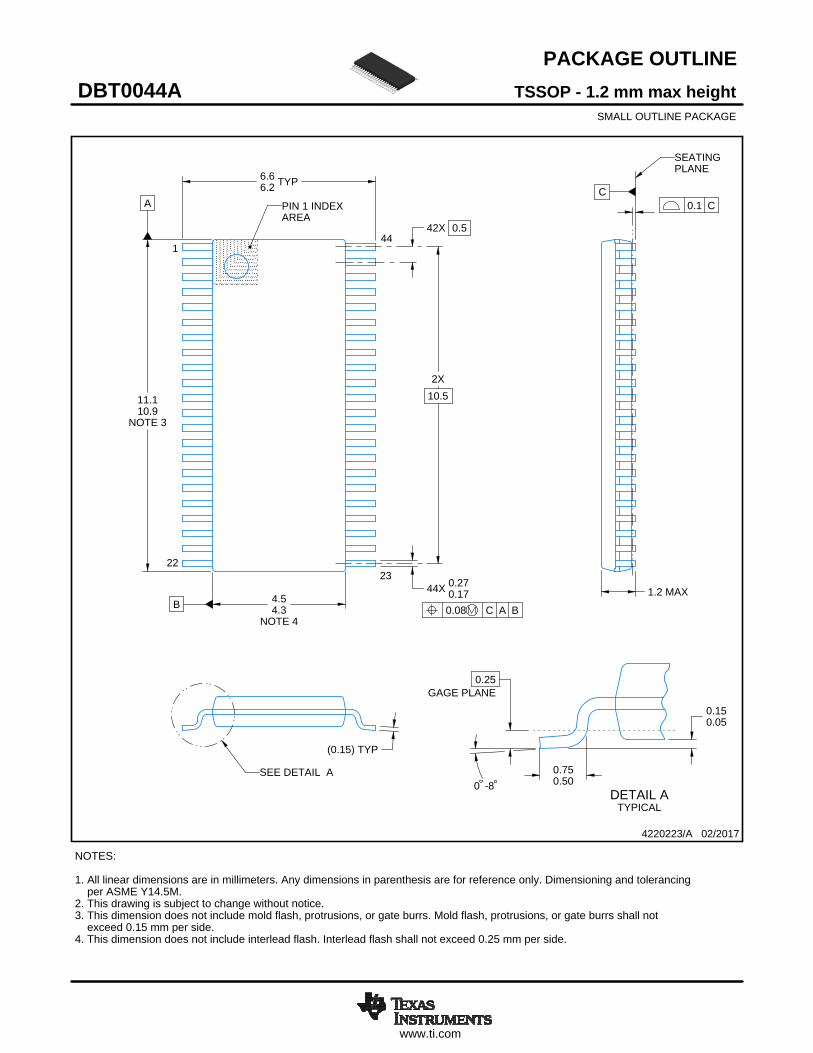
www.ti.com
PACKAGE OUTLINE
C
42X 0.5
2X10.5
44X 0.270.17
TYP6.66.2
1.2 MAX
0.150.05
0.25GAGE PLANE
-80
BNOTE 4
4.54.3
A
NOTE 3
11.110.9
0.750.50
(0.15) TYP
TSSOP - 1.2 mm max heightDBT0044ASMALL OUTLINE PACKAGE
4220223/A 02/2017
1
2223
44
0.08 C A B
PIN 1 INDEXAREA
SEE DETAIL A
0.1 C
NOTES: 1. All linear dimensions are in millimeters. Any dimensions in parenthesis are for reference only. Dimensioning and tolerancing per ASME Y14.5M. 2. This drawing is subject to change without notice. 3. This dimension does not include mold flash, protrusions, or gate burrs. Mold flash, protrusions, or gate burrs shall not exceed 0.15 mm per side. 4. This dimension does not include interlead flash. Interlead flash shall not exceed 0.25 mm per side.
SEATINGPLANE
A 20DETAIL ATYPICAL
SCALE 1.500

www.ti.com
EXAMPLE BOARD LAYOUT
0.05 MAXALL AROUND
0.05 MINALL AROUND
44X (1.5)
44X (0.3)
42X (0.5)
(5.8)
(R0.05) TYP
TSSOP - 1.2 mm max heightDBT0044ASMALL OUTLINE PACKAGE
4220223/A 02/2017
NOTES: (continued) 5. Publication IPC-7351 may have alternate designs. 6. Solder mask tolerances between and around signal pads can vary based on board fabrication site.
LAND PATTERN EXAMPLEEXPOSED METAL SHOWN
SCALE: 8X
SYMM
SYMM
1
22 23
44
15.000
METALSOLDER MASKOPENING
METAL UNDERSOLDER MASK
SOLDER MASKOPENING
EXPOSED METALEXPOSED METAL
SOLDER MASK DETAILS
NON-SOLDER MASKDEFINED
(PREFERRED)
SOLDER MASKDEFINED

www.ti.com
EXAMPLE STENCIL DESIGN
44X (1.5)
44X (0.3)
42X (0.5)
(5.8)
(R0.05) TYP
TSSOP - 1.2 mm max heightDBT0044ASMALL OUTLINE PACKAGE
4220223/A 02/2017
NOTES: (continued) 7. Laser cutting apertures with trapezoidal walls and rounded corners may offer better paste release. IPC-7525 may have alternate design recommendations. 8. Board assembly site may have different recommendations for stencil design.
SOLDER PASTE EXAMPLEBASED ON 0.125 mm THICK STENCIL
SCALE: 8X
SYMM
SYMM
1
22 23
44

IMPORTANT NOTICE
Texas Instruments Incorporated (TI) reserves the right to make corrections, enhancements, improvements and other changes to itssemiconductor products and services per JESD46, latest issue, and to discontinue any product or service per JESD48, latest issue. Buyersshould obtain the latest relevant information before placing orders and should verify that such information is current and complete.TI’s published terms of sale for semiconductor products (http://www.ti.com/sc/docs/stdterms.htm) apply to the sale of packaged integratedcircuit products that TI has qualified and released to market. Additional terms may apply to the use or sale of other types of TI products andservices.Reproduction of significant portions of TI information in TI data sheets is permissible only if reproduction is without alteration and isaccompanied by all associated warranties, conditions, limitations, and notices. TI is not responsible or liable for such reproduceddocumentation. Information of third parties may be subject to additional restrictions. Resale of TI products or services with statementsdifferent from or beyond the parameters stated by TI for that product or service voids all express and any implied warranties for theassociated TI product or service and is an unfair and deceptive business practice. TI is not responsible or liable for any such statements.Buyers and others who are developing systems that incorporate TI products (collectively, “Designers”) understand and agree that Designersremain responsible for using their independent analysis, evaluation and judgment in designing their applications and that Designers havefull and exclusive responsibility to assure the safety of Designers' applications and compliance of their applications (and of all TI productsused in or for Designers’ applications) with all applicable regulations, laws and other applicable requirements. Designer represents that, withrespect to their applications, Designer has all the necessary expertise to create and implement safeguards that (1) anticipate dangerousconsequences of failures, (2) monitor failures and their consequences, and (3) lessen the likelihood of failures that might cause harm andtake appropriate actions. Designer agrees that prior to using or distributing any applications that include TI products, Designer willthoroughly test such applications and the functionality of such TI products as used in such applications.TI’s provision of technical, application or other design advice, quality characterization, reliability data or other services or information,including, but not limited to, reference designs and materials relating to evaluation modules, (collectively, “TI Resources”) are intended toassist designers who are developing applications that incorporate TI products; by downloading, accessing or using TI Resources in anyway, Designer (individually or, if Designer is acting on behalf of a company, Designer’s company) agrees to use any particular TI Resourcesolely for this purpose and subject to the terms of this Notice.TI’s provision of TI Resources does not expand or otherwise alter TI’s applicable published warranties or warranty disclaimers for TIproducts, and no additional obligations or liabilities arise from TI providing such TI Resources. TI reserves the right to make corrections,enhancements, improvements and other changes to its TI Resources. TI has not conducted any testing other than that specificallydescribed in the published documentation for a particular TI Resource.Designer is authorized to use, copy and modify any individual TI Resource only in connection with the development of applications thatinclude the TI product(s) identified in such TI Resource. NO OTHER LICENSE, EXPRESS OR IMPLIED, BY ESTOPPEL OR OTHERWISETO ANY OTHER TI INTELLECTUAL PROPERTY RIGHT, AND NO LICENSE TO ANY TECHNOLOGY OR INTELLECTUAL PROPERTYRIGHT OF TI OR ANY THIRD PARTY IS GRANTED HEREIN, including but not limited to any patent right, copyright, mask work right, orother intellectual property right relating to any combination, machine, or process in which TI products or services are used. Informationregarding or referencing third-party products or services does not constitute a license to use such products or services, or a warranty orendorsement thereof. Use of TI Resources may require a license from a third party under the patents or other intellectual property of thethird party, or a license from TI under the patents or other intellectual property of TI.TI RESOURCES ARE PROVIDED “AS IS” AND WITH ALL FAULTS. TI DISCLAIMS ALL OTHER WARRANTIES ORREPRESENTATIONS, EXPRESS OR IMPLIED, REGARDING RESOURCES OR USE THEREOF, INCLUDING BUT NOT LIMITED TOACCURACY OR COMPLETENESS, TITLE, ANY EPIDEMIC FAILURE WARRANTY AND ANY IMPLIED WARRANTIES OFMERCHANTABILITY, FITNESS FOR A PARTICULAR PURPOSE, AND NON-INFRINGEMENT OF ANY THIRD PARTY INTELLECTUALPROPERTY RIGHTS. TI SHALL NOT BE LIABLE FOR AND SHALL NOT DEFEND OR INDEMNIFY DESIGNER AGAINST ANY CLAIM,INCLUDING BUT NOT LIMITED TO ANY INFRINGEMENT CLAIM THAT RELATES TO OR IS BASED ON ANY COMBINATION OFPRODUCTS EVEN IF DESCRIBED IN TI RESOURCES OR OTHERWISE. IN NO EVENT SHALL TI BE LIABLE FOR ANY ACTUAL,DIRECT, SPECIAL, COLLATERAL, INDIRECT, PUNITIVE, INCIDENTAL, CONSEQUENTIAL OR EXEMPLARY DAMAGES INCONNECTION WITH OR ARISING OUT OF TI RESOURCES OR USE THEREOF, AND REGARDLESS OF WHETHER TI HAS BEENADVISED OF THE POSSIBILITY OF SUCH DAMAGES.Unless TI has explicitly designated an individual product as meeting the requirements of a particular industry standard (e.g., ISO/TS 16949and ISO 26262), TI is not responsible for any failure to meet such industry standard requirements.Where TI specifically promotes products as facilitating functional safety or as compliant with industry functional safety standards, suchproducts are intended to help enable customers to design and create their own applications that meet applicable functional safety standardsand requirements. Using products in an application does not by itself establish any safety features in the application. Designers mustensure compliance with safety-related requirements and standards applicable to their applications. Designer may not use any TI products inlife-critical medical equipment unless authorized officers of the parties have executed a special contract specifically governing such use.Life-critical medical equipment is medical equipment where failure of such equipment would cause serious bodily injury or death (e.g., lifesupport, pacemakers, defibrillators, heart pumps, neurostimulators, and implantables). Such equipment includes, without limitation, allmedical devices identified by the U.S. Food and Drug Administration as Class III devices and equivalent classifications outside the U.S.TI may expressly designate certain products as completing a particular qualification (e.g., Q100, Military Grade, or Enhanced Product).Designers agree that it has the necessary expertise to select the product with the appropriate qualification designation for their applicationsand that proper product selection is at Designers’ own risk. Designers are solely responsible for compliance with all legal and regulatoryrequirements in connection with such selection.Designer will fully indemnify TI and its representatives against any damages, costs, losses, and/or liabilities arising out of Designer’s non-compliance with the terms and provisions of this Notice.
Mailing Address: Texas Instruments, Post Office Box 655303, Dallas, Texas 75265Copyright © 2017, Texas Instruments Incorporated
![Fujitsu Touch Panel (Serial) Device driver setting manual · PDF fileFujitsu Touch Panel (Serial) Device driver setting manual ... [Arrow keys] : Move the ... Serial RTP driver manual](https://img.dokumen.tips/doc/110x75/5a8f4b457f8b9abb068d8816/fujitsu-touch-panel-serial-device-driver-setting-manual-touch-panel-serial-device.jpg)