Embed Size (px)
Citation preview

TPAC1.1 Testing
JC/Jan 16th

Comparator Investigations• Two (related) symptoms were observed
– Non-gaussian threshold scans, with steep sides and flat tops– Test pixel comparator oscillates for very low thresholds
• Coupling (positive feedback) in the pixel design– Not present (or significantly diminished) in old pixel design– Dominant in new pixel design causing oscillations– Schematic is fundamentally the same, so must be due to layout parasitic capacitance
• Full RCX simulation– Fixed a bug (previously caused full pixel RCX to fail)– Setting a very low threshold shows oscillations!
• Good any fix should be possible to prove in simulation• Previously all RCX simulations had not checked the very low threshold case, which is necessary to cause
oscillation• Pixel performs ok at higher thresholds, although some injection can be seen that might have identified a
potential problem
– Doesn’t actually identify the problem, just confirms that one exists
• Analysis of circuit and observed behaviour is required to understand what is going on
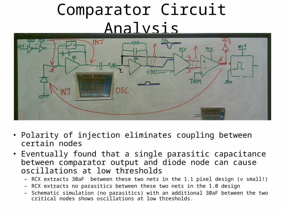
Comparator Circuit Analysis
• Polarity of injection eliminates coupling between certain nodes• Eventually found that a single parasitic capacitance between
comparator output and diode node can cause oscillations at low thresholds– RCX extracts 30aF between these two nets in the 1.1 pixel design (v small!)– RCX extracts no parasitics between these two nets in the 1.0 design – Schematic simulation (no parasitics) with an additional 30aF between the two critical nodes
shows oscillations at low thresholds.

Sanity check
• Can 30aF really matter?– Would not normally consider such tiny parasitics!– But… diode node is sensitive to induced charge, with
a large gain…
Consider a switching 1.8v signal coupling through a 30aF capacitor…
Q = 30 x10-18 * 1.8 = 5.4 x10⁻¹⁷ C= 337 electrons
Circuit charge gain is ~140uV/e- so… = 47mV signal
!

TPAC1.0 preShape
pixel layout
Comparator output
M1 M2 M3 M4
Comparator output bridges diode node only once, on metal 4 with metal 3 shield.

TPAC1.1 preShape
pixel layout
Comparator output
M1 M2 M3
Comparator output was re-routed in v1.1 over SRAMS but crossing diode node twice
No M2 shield at one crossing creates dominant capacitance between the two nets

TPAC1.2 preShape
pixel layout
Comparator output
M1 M2 M3
Single mask change (M2)Extended shielding (ground)
RCX tool finds no parasitics between comparator output and diode node
?

Simulation SummaryDesign View Cpara
(HIT DIODE)
Cpara(DIODE GND)
GainμV/e-
Simulation
Original 1.0
Schematic 0 14 (est) 118
Extracted (C only) 0 13 164
Extracted (sel RC) 0 13.3 164
Revision 1.1
Schematic 0 14 (est) 136
Extracted (C only) 30.25a 12.1 182 Oscillates at low Vth
Extracted (sel RC) 27.9a 12.4 181 Oscillates at low Vth
Amended1.2
Schematic 0 14 (est) 160
Extracted (C only) 0 12.5 180
Extracted (sel RC) 0 12.8 178

Comments• Suggested fix adds small additional parasitics to
diode node, but acceptable within context of original design
• Unsure of reliability of parasitic extraction tools at this precision (10-18) – what error bars to apply?
• Small injection effects are seen in the v1.0 test pixel – which the RCX tool does not predict– but the pixel does operate properly

Measured Injection• Cross check size of injected signal with predicted
coupling capacitance– Charge gain known from marcel’s 55Fe test pixel results– Can observe signals at two points in analog chain
• Induced signal on shaper output– Varies, in range 1724mV
• Note: Corresponding injection on shaper input will be too small to see on scope (<1mV)
– Applying a gain of 150uV/e-– Injection varies in range 113160e-
• Right order of magnitude!

Mask change costs
• M2 required to fix parasitic capacitance• CS required to fix address repettition
• $$…

Spare slides
• Signals during oscillation – Triggered by noise– Oscillation– Similar scope trace

Signals
Diode
Preamp out
Shaper out
Comparator
Threshold

Signals
Diode
Preamp out
Shaper out
Comparator
Threshold

Signals
Diode
Preamp out
Shaper out
Comparator
Threshold

Signals
Diode
Preamp out
Shaper out
Comparator
Threshold

Signals
Diode
Preamp out
Shaper out
Comparator
Threshold
etc…

Signals
Diode
Preamp out
Shaper out
Comparator